JP4937700B2 - Dry polishing equipment - Google Patents
Dry polishing equipment Download PDFInfo
- Publication number
- JP4937700B2 JP4937700B2 JP2006301856A JP2006301856A JP4937700B2 JP 4937700 B2 JP4937700 B2 JP 4937700B2 JP 2006301856 A JP2006301856 A JP 2006301856A JP 2006301856 A JP2006301856 A JP 2006301856A JP 4937700 B2 JP4937700 B2 JP 4937700B2
- Authority
- JP
- Japan
- Prior art keywords
- polishing
- wafer
- holding
- dry
- semiconductor wafer
- Prior art date
- Legal status (The legal status is an assumption and is not a legal conclusion. Google has not performed a legal analysis and makes no representation as to the accuracy of the status listed.)
- Active
Links
- 238000005498 polishing Methods 0.000 title claims description 119
- 230000003068 static effect Effects 0.000 claims description 27
- 239000004065 semiconductor Substances 0.000 claims description 23
- 230000005611 electricity Effects 0.000 claims description 12
- 239000004020 conductor Substances 0.000 claims description 5
- OKTJSMMVPCPJKN-UHFFFAOYSA-N Carbon Chemical compound [C] OKTJSMMVPCPJKN-UHFFFAOYSA-N 0.000 claims description 4
- 229920000049 Carbon (fiber) Polymers 0.000 claims description 3
- 229910052799 carbon Inorganic materials 0.000 claims description 3
- 239000004917 carbon fiber Substances 0.000 claims description 3
- 238000013459 approach Methods 0.000 claims description 2
- 238000009837 dry grinding Methods 0.000 claims 1
- 230000003472 neutralizing effect Effects 0.000 claims 1
- 235000012431 wafers Nutrition 0.000 description 70
- 238000012545 processing Methods 0.000 description 12
- 238000011084 recovery Methods 0.000 description 9
- 238000004140 cleaning Methods 0.000 description 8
- 230000008030 elimination Effects 0.000 description 7
- 238000003379 elimination reaction Methods 0.000 description 7
- 238000000034 method Methods 0.000 description 7
- 238000012546 transfer Methods 0.000 description 6
- XLYOFNOQVPJJNP-UHFFFAOYSA-N water Substances O XLYOFNOQVPJJNP-UHFFFAOYSA-N 0.000 description 6
- 239000006061 abrasive grain Substances 0.000 description 4
- 239000011230 binding agent Substances 0.000 description 4
- 239000000853 adhesive Substances 0.000 description 3
- 230000001070 adhesive effect Effects 0.000 description 3
- PNEYBMLMFCGWSK-UHFFFAOYSA-N aluminium oxide Inorganic materials [O-2].[O-2].[O-2].[Al+3].[Al+3] PNEYBMLMFCGWSK-UHFFFAOYSA-N 0.000 description 3
- 230000006378 damage Effects 0.000 description 3
- 229920001971 elastomer Polymers 0.000 description 3
- 239000000463 material Substances 0.000 description 3
- 230000002093 peripheral effect Effects 0.000 description 3
- 239000005060 rubber Substances 0.000 description 3
- 229920000459 Nitrile rubber Polymers 0.000 description 2
- 229910000420 cerium oxide Inorganic materials 0.000 description 2
- 238000005530 etching Methods 0.000 description 2
- 239000004744 fabric Substances 0.000 description 2
- 238000003754 machining Methods 0.000 description 2
- 238000012986 modification Methods 0.000 description 2
- 230000004048 modification Effects 0.000 description 2
- 239000004745 nonwoven fabric Substances 0.000 description 2
- BMMGVYCKOGBVEV-UHFFFAOYSA-N oxo(oxoceriooxy)cerium Chemical compound [Ce]=O.O=[Ce]=O BMMGVYCKOGBVEV-UHFFFAOYSA-N 0.000 description 2
- 238000003825 pressing Methods 0.000 description 2
- 230000001681 protective effect Effects 0.000 description 2
- 229920003048 styrene butadiene rubber Polymers 0.000 description 2
- YCKRFDGAMUMZLT-UHFFFAOYSA-N Fluorine atom Chemical compound [F] YCKRFDGAMUMZLT-UHFFFAOYSA-N 0.000 description 1
- 229920002396 Polyurea Polymers 0.000 description 1
- XUIMIQQOPSSXEZ-UHFFFAOYSA-N Silicon Chemical compound [Si] XUIMIQQOPSSXEZ-UHFFFAOYSA-N 0.000 description 1
- 239000002174 Styrene-butadiene Substances 0.000 description 1
- 239000003082 abrasive agent Substances 0.000 description 1
- 239000013078 crystal Substances 0.000 description 1
- 238000005520 cutting process Methods 0.000 description 1
- 239000000428 dust Substances 0.000 description 1
- 230000000694 effects Effects 0.000 description 1
- 238000010292 electrical insulation Methods 0.000 description 1
- 238000007667 floating Methods 0.000 description 1
- 239000011737 fluorine Substances 0.000 description 1
- 229910052731 fluorine Inorganic materials 0.000 description 1
- 238000012423 maintenance Methods 0.000 description 1
- 238000006386 neutralization reaction Methods 0.000 description 1
- 238000007517 polishing process Methods 0.000 description 1
- 229920000098 polyolefin Polymers 0.000 description 1
- 229920005989 resin Polymers 0.000 description 1
- 239000011347 resin Substances 0.000 description 1
- 229910052710 silicon Inorganic materials 0.000 description 1
- 239000010703 silicon Substances 0.000 description 1
- HBMJWWWQQXIZIP-UHFFFAOYSA-N silicon carbide Chemical compound [Si+]#[C-] HBMJWWWQQXIZIP-UHFFFAOYSA-N 0.000 description 1
- 229910010271 silicon carbide Inorganic materials 0.000 description 1
- 229920002379 silicone rubber Polymers 0.000 description 1
- 239000004945 silicone rubber Substances 0.000 description 1
- 239000002002 slurry Substances 0.000 description 1
- 238000005507 spraying Methods 0.000 description 1
- 239000000126 substance Substances 0.000 description 1
Images


Description
本発明は、被加工物である半導体ウェーハを乾式研磨する乾式研磨装置に係り、特に、半導体ウェーハを帯電させることなく研磨する技術に関する。 The present invention relates to a dry polishing apparatus for dry polishing a semiconductor wafer as a workpiece, and more particularly to a technique for polishing a semiconductor wafer without charging.
表面に複数の半導体デバイスを形成したウェーハは、バックグラインド工程などによって必要な厚みに仕上げられた後にダイシングテープに貼着され、ダイシング装置などによって個々のデバイスチップに分割されるのが一般的である。昨今の電子機器の軽薄短小化に対応するため、必要な厚みは100μm以下となり、チップ化した後のチップとしての強度の維持が問題となっている。そこで、バックグラインドした後に加工面を研磨やエッチングすることで、バックグラインドによる機械的ダメージを除去する技術が用いられている。そのような技術として、たとえば特許文献1には、エッチング用の薬液やスラリーを使用することなく研磨可能な乾式研磨砥石を用いる技術が開示されている。
In general, a wafer having a plurality of semiconductor devices formed on the surface is finished to a required thickness by a back grinding process or the like, and then attached to a dicing tape, and then divided into individual device chips by a dicing apparatus or the like. . In order to cope with the recent downsizing of electronic devices, the necessary thickness is 100 μm or less, and the maintenance of the strength as a chip after being formed into a chip is a problem. Therefore, a technique is used in which mechanical damage due to back grinding is removed by polishing or etching the processed surface after back grinding. As such a technique, for example,
乾式研磨の場合は、研磨砥石と被加工物である半導体ウェーハを乾燥した状態を維持しながら擦り合わせることによって研磨加工するため、半導体ウェーハに静電気が帯電する。この帯電した静電気が何らかのタイミングで半導体ウェーハ表面に形成されたデバイスに通電すると、デバイスを破壊する恐れがある。 In the case of dry polishing, since polishing is performed by rubbing a polishing grindstone and a semiconductor wafer as a workpiece while maintaining a dry state, static electricity is charged on the semiconductor wafer. If this charged static electricity is applied to a device formed on the surface of the semiconductor wafer at some timing, the device may be destroyed.
したがって、本発明は、上記のような従来技術の問題を解決するためになされたもので、加工中のウェーハが帯電するのを防止することができる乾式研磨装置を提供することを目的としている。 Accordingly, the present invention has been made to solve the above-described problems of the prior art, and an object thereof is to provide a dry polishing apparatus capable of preventing the wafer being processed from being charged.
本発明は、半導体ウェーハを乾式研磨するための乾式研磨装置であって、半導体ウェーハを回転可能に吸着保持する保持手段と、研磨砥石を回転可能に保持する研磨手段と、研磨手段を保持手段の保持面に対して垂直方向に接近離間可能とする送り手段と、保持手段と研磨手段を保持手段の保持面に平行な方向に相対的に接近離間させる移動手段とを具備し、研磨手段は、円盤状のフレームの片面に保持面に対向させられる研磨砥石が固着されてなり、該研磨砥石は、研磨砥粒を含み研磨面を形成する研磨部と、フレームに接触するとともに、該研磨面に表出するとともに研磨部と分けられた状態で円周方向に等間隔に配置された炭素または炭素繊維からなる導電性材料を含む除電部とを備え、半導体ウェーハに発生する静電気を、除電部を介してフレームに流して除電することを特徴としている。 The present invention is a dry polishing apparatus for dry polishing a semiconductor wafer, comprising: a holding unit that rotatably holds a semiconductor wafer; a polishing unit that rotatably holds a polishing grindstone; and a polishing unit that holds the polishing unit. A feed unit that allows the holding unit to approach and separate in a direction perpendicular to the holding surface; and a moving unit that relatively moves the holding unit and the polishing unit in a direction parallel to the holding surface of the holding unit. A polishing grindstone that is opposed to the holding surface is fixed to one surface of a disk-shaped frame, and the polishing grindstone includes a polishing portion that includes polishing abrasive grains and forms a polishing surface, and contacts the frame, and is attached to the polishing surface. and a static eliminator which comprises an electrically conductive material composed of equally spaced carbon or carbon fibers in the circumferential direction in a state of being separated from the polishing unit while exposed, the static electricity generated in the semiconductor wafer, the discharger It is characterized for discharge flowing to the frame.
本発明によれば、半導体ウェーハに発生する静電気は研磨手段の導電性材料を含む除電部からフレームを通って装置本体に流れ、そこから接地電流として放散される。したがって、本発明では、帯電した静電気がデバイスに通電することによって生じるデバイスの破壊等の発生を未然に防止することができる。 According to the present invention, static electricity generated in the semiconductor wafer flows from the static eliminating portion including the conductive material of the polishing means through the frame to the apparatus main body, and is dissipated therefrom as a ground current. Therefore, in the present invention, it is possible to prevent the occurrence of destruction of the device caused by electrified static electricity passing through the device.
研磨砥石は、研磨砥粒および結合材からなる研磨部と、導電性材料および結合材からなる除電部とを分けて形成し、研磨部に除電部が円周方向に等間隔に配置して構成される。この場合、除電部が島状に散在したり、放射状に延在するように構成することができる。 The grinding wheel is composed of a polishing part made of abrasive grains and a binder and a charge removal part made of a conductive material and a binder, and the charge removal parts are arranged at equal intervals in the circumferential direction in the polishing part. Is done. In this case, it can be configured such that the static eliminating portions are scattered in an island shape or extend radially.
本発明によれば、半導体ウェーハに発生する静電気は研磨手段の導電性材料を含む除電部を介して除電されるから、帯電した静電気がデバイスに通電することによって生じるデバイスの破壊等の発生を未然に防止することができる。 According to the present invention, the static electricity generated in the semiconductor wafer is neutralized through the static eliminating portion including the conductive material of the polishing means. Can be prevented.
以下、図面を参照して本発明に係る乾式研磨装置の一実施形態を説明する。
[1]半導体ウエーハ
図1の符号1は、一実施形態の乾式研磨装置によって裏面が研磨される円板状の半導体ウエーハ(以下ウエーハと略称)を示している。このウエーハ1はシリコンウエーハ等であって、研削工程によって裏面が例えば600〜700μmから100μm以下の厚みに加工されたものである。ウエーハ1の表面には、格子状の分割予定ライン2によって複数の矩形状の半導体チップ3が区画されており、これら半導体チップ3の表面には、ICやLSI等の図示せぬ電子回路が形成されている。
Hereinafter, an embodiment of a dry polishing apparatus according to the present invention will be described with reference to the drawings.
[1] Semiconductor
ウエーハ1の周面の所定箇所には、半導体の結晶方位を示すV字状のノッチ6が形成されている。ウエーハ1は、最終的には分割予定ライン2に沿って切断、分割され、複数の半導体チップ3に個片化される。ウエーハ1を裏面研削および乾式研磨する際には、電子回路を保護するなどの目的で、図1に示すように電子回路が形成された側の表面に保護テープ7が貼着される。保護テープ7は、例えば厚さ70〜200μm程度のポリオレフィン等の柔らかい樹脂製基材シートの片面に5〜20μm程度の粘着剤を塗布した構成のものが用いられ、粘着剤をウエーハ1の裏面に合わせて貼り付けられる。
A V-shaped notch 6 indicating the crystal orientation of the semiconductor is formed at a predetermined location on the peripheral surface of the
[2]研磨加工装置
図2は、一実施形態の乾式研磨装置を示している。この乾式研磨装置10は、直方体状の基台11を備えている。この基台11の長手方向一端部には、基台11の水平な上面に対して垂直に立設された壁部12が一体に形成されている。図2では、基台11の長手方向、幅方向および鉛直方向を、それぞれY方向、X方向およびZ方向で示している。基台11上は、長手方向のほぼ中間部分から壁部12側がウェーハ1を加工する加工エリア11Aとされ、この反対側が、加工エリア11Aに加工前のウェーハ1を供給し、かつ、加工後のウェーハ1を回収する着脱エリア11Bとされている。
以下、加工エリア11Aと着脱エリア11Bについて説明する。
[2] Polishing Apparatus FIG. 2 shows a dry polishing apparatus according to an embodiment. The
Hereinafter, the
(a)加工エリアの機構
図2に示すように、加工エリア11Aには矩形状のピット13が形成されている。このピット13内には、テーブルベース(移動手段)14を介して真空チャック式の円盤状のチャックテーブル(保持手段)15がY方向に移動自在に設けられている。テーブルベース14は、ピット13内に配されたY方向に延びるガイドレールに摺動自在に設けられており、適宜な駆動機構(いずれも図示略)によって同方向を往復動させられる。また、チャックテーブル15は、アルミナやシリコンカーバイトなどで構成され、ウェーハ1との電気的絶縁性が確保されて半導体チップ3への通電が防止されている。
(A) Mechanism of machining area As shown in FIG. 2,
テーブルベース14の移動方向両端部には蛇腹状のカバー16,17の一端がそれぞれ取り付けられており、これらカバー16,17の他端は、壁部12の内面と、壁部12に対向するピット13の内壁面に、それぞれ取り付けられている。これら、カバー16,17は、テーブルベース14の移動路を覆い、その移動路に研磨屑等が落下することを防ぐもので、テーブルベース14の移動に伴って伸縮する。チャックテーブル15は、テーブルベース14上に、ウェーハ1の保持面である上面が水平な状態とされ、かつ、Z方向(鉛直方向)に沿った図示せぬ回転軸を中心にして回転自在に支持されている。チャックテーブル15は、図示せぬ回転駆動機構によって時計方向または反時計方向に回転可能となっている。
One end of bellows-
チャックテーブル15は、図2に示すようにテーブルベース14ごと壁部12側に移動して所定の研磨加工位置に位置付けられる。その研磨加工位置の上方には、研磨ユニット20が配されている。この研磨ユニット20は、基台11の壁部12に、移動板32およびガイドレール31を介して昇降自在に取り付けられ、モータ30によって駆動する送り機構(送り手段)33によって昇降させられる。
As shown in FIG. 2, the chuck table 15 is moved together with the
研磨ユニット20は、図2および図3に示すように、軸方向がZ方向に延びる円筒状のスピンドルハウジング21と、このスピンドルハウジング21内に、図示せぬエアーベアリング機構によって同軸的、かつ回転自在に支持されたスピンドルシャフト22と、スピンドルハウジング21の上端部に固定されてスピンドルシャフト22を回転駆動するモータ23と、スピンドルシャフト22の下端に同軸的に固定された円盤状のフランジ24と、フランジ24の下面に固定された研磨工具(研磨手段)50とを具備している。図2に示すように、研磨ユニット20は、スピンドルハウジング21がブロック34を介して移動板32に固定されている。
As shown in FIGS. 2 and 3, the
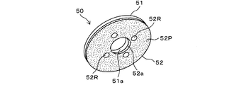
研磨工具50は、図4にも示すように、外径がフランジ24とほぼ同径の円盤状のフレーム51の下面に、円盤状の研磨パッド(研磨砥石)52が固着されたものである。フレーム51の中央部には貫通孔51aが形成され、研磨パッド52の中央部にも同形同大の貫通孔52aが形成されており、フレーム51および研磨パッド52はフランジ24に対して同心状に配されている。研磨パッド52は、不織布等からなる研磨用布中にアルミナや酸化セリウム等の研磨砥粒を含浸させて適宜の結合材によって結合することにより、円板状に成形されている。研磨パッド52の殆どは、研磨に供される研磨部52Pであり、この研磨部52Pには、複数(この実施形態では4つ)の除電部52Rが円周方向に等間隔に配置されている。
As shown in FIG. 4, the
除電部52Rは、研磨部52Pを軸線方向に円形にくり抜いて埋設されている。除電部52Rは、不織布等に炭素粉末を含浸させて結合材によって結合させたり、炭素繊維を結合材で固めたりすることで形成され、図4および図7に示すように、その一端面は研磨部52Pと面一となり、他端面がフレーム51に接触している。これにより、研磨パッド52によりウェーハ1を乾式研磨すると、ウェーハ1とフレーム51とが導通する。
The
上記のように構成された研磨パッド52は、接着手段等によってフレーム51に固着されている。研磨工具50は、フレーム51がフランジ24にねじ止め等によって取り付けられることにより、研磨ユニット20に着脱自在にセットされる。
The
(b)着脱エリアの機構
図2に示すように、着脱エリア11Bの中央には矩形状のピット18が形成されており、このピット18の底部には、上下移動する2節リンク式の移送ロボット60が設置されている。そしてこの移送ロボット60の周囲には、上から見た状態で反時計回りに、供給カセット61、位置合わせ台62、旋回アーム式の供給アーム63、供給アーム63と同じ構造の回収アーム64、スピンナ式の洗浄装置65、回収カセット66が、それぞれ配置されている。
(B) Mechanism of attachment / detachment area As shown in FIG. 2, a
供給カセット61、位置合わせ台62および供給アーム63はウェーハ1をチャックテーブル15に供給する手段であり、回収アーム64、洗浄装置65および回収カセット66は、研磨が終了したウェーハ1をチャックテーブル15から回収する手段である。各カセット61,66は複数のウェーハ1を積層状態で収容するもので、基台11上の所定位置にセットされる。
The
移送ロボット60によって供給カセット61内から1枚のウェーハ1が取り出されると、そのウェーハ1は被加工面を上に向けて位置合わせ台62上に載置され、ここで一定の位置に決められる。次いでウェーハ1は、供給アーム63によって位置合わせ台62から吸着されて取り上げられ、着脱位置で待機しているチャックテーブル15上に被加工面を上に向けた状態に載置される。一方、研磨ユニット20によって被加工面が研磨され、着脱位置に位置付けられたチャックテーブル15上のウェーハ1は回収アーム64によって吸着されて取り上げられ、洗浄装置65に移されて水洗、乾燥される。そして、洗浄装置65で洗浄処理されたウェーハ1は、移送ロボット60によって回収カセット66内に移送、収容される。
When one
供給アーム63と回収アーム64の間には、チャックテーブル15に洗浄水および高圧エアーを噴射してチャックテーブル15を洗浄するノズル67が配されている。研磨ユニット20によるウェーハ1の加工位置は、着脱位置よりも壁部12側に所定距離移動した範囲とされ、チャックテーブル15は、テーブルベース14の移動によって、これら加工位置と着脱位置との間を行き来させられる。ノズル67によるチャックテーブル15の洗浄、および水の供給は、着脱位置において行われる。
A
[3]研磨動作
次に、乾式研磨装置10を用いて薄板状のウェーハ1を乾式研磨する方法を説明する。まず、供給カセット61内に、多数のウェーハ1を収容する。そのうちの1枚のウェーハ1が、移送ロボット60によって位置合わせ台62に移され、位置決めされる。続いて供給アーム63によって、着脱位置で待機し、かつ真空運転されているチャックテーブル15上に、研磨を施すべき被加工面を上に向けて露出させられたウェーハ1が載置される。ウェーハ1は、チャックテーブル15の上面に吸着して保持される。チャックテーブル15の吸着エリアは、ウェーハ1の形状に応じた形状に設定されることが望ましい。なお、この実施形態のチャックテーブル15は真空チャック式であるが、被加工面を露出した状態でウェーハ1を保持できる形式であれば、チャック方式はいかなる形式であってもよい。
[3] Polishing Operation Next, a method for dry polishing the
次に、テーブルベース14が壁部12方向に移動し、ウェーハ1が研磨ユニット20の下方の研磨加工位置に送り込まれる。そして、チャックテーブル15が回転してウェーハ1が回転させられ、このウェーハ1に、送り機構33によって下降させた研磨ユニット20を近付けるとともに、モータ23のスピンドルシャフト22を高速回転させて研磨工具50の研磨パッド52をウェーハ1の被加工面に押圧させ、研磨パッド52によってウェーハ1の被加工面を乾式研磨する。
Next, the
ウェーハ1すなわちチャックテーブル15の回転数や回転方向、研磨工具50の回転数や回転方向、ならびにウェーハ1に対する研磨パッド52の荷重等の運転条件は、ウェーハ1の材質等によって任意に設定されるが、例えば、ウェーハ1と研磨パッド52は互いに反対方向に回転し、ウェーハ1の回転数は100〜300rpm、研磨パッド52の回転数は1000〜3000rpmといった条件で研磨加工される。また、研磨パッド52のウェーハ1に対する押圧力は50〜500Nに設定される。なお、押圧力の制御は、例えばチャックテーブル15の下方に配した力センサ(例えば日本キスラー社製:薄型力センサ9135B等)によって逐一計測しながら行うことが可能である。
The operating conditions such as the rotation speed and rotation direction of the
なお、図3では、研磨パッド52はウェーハ1よりも大きく、ウェーハ1の全面を覆って研磨しているが、研磨パッド52の大きさはウェーハ1より小さくてもよい。しかしながら、加工効率の観点からはできるだけ研磨パッド52は大きいものの方が好ましい。
In FIG. 3, the
ウェーハ1の被加工面が所望の度合いに研磨加工されたら、研磨ユニット20を上昇させて研磨パッド52をウェーハ1から離すとともに、チャックテーブル15の回転を停止させる。そして、テーブルベース14を着脱位置に移動させるとともに、チャックテーブル15の真空運転を停止させる。この後、ウェーハ1は、回収アーム64によって洗浄装置65内に移送されて水洗されてから水分が除去され、次いで、移送ロボット60によって回収カセット66内に移送、収容される。また、ノズル67から、供給・回収位置で停止しているチャックテーブル15に向けて洗浄水と高圧エアーが噴射され、チャックテーブル15が洗浄される。
When the processing surface of the
[4]一実施形態の作用効果
上記のようにして、研磨パッド52によってウェーハ1の被加工面を乾式研磨すると、両者の摩擦によって静電気が発生する。この場合において、図3に示すように、研磨パッドの除電部52Rは、ウェーハ1に常に接触しているから、発生した静電気は除電部52Rを介してフレーム51に流れ、フレーム51からスピンドルシャフト22等を伝わって接地電流として放散される。ここで、スピンドルシャフト22はスピンドルハウジング21内にエアーベアリング機構によって浮上した状態で支持されているが、静電気は導通することができる。すなわち、エアーベアリング機構のスラストベアリングの表面には、焼付きを防止するためにカーボン板などが埋め込まれ、しかも、スラストベアリングのクリアランスは極めて僅かである。そして、導電性が良く隙間が極小であるため、静電気は容易に導通することができ、乾式研磨装置10の各部を導通して放散される。したがって、帯電した静電気がウェーハ1の半導体チップ3に通電することによって生じる半導体チップ3の破壊等の発生を未然に防止することができる。
[4] Effects of One Embodiment When the work surface of the
[5]変更例
除電部52Rは、上記実施形態のものに限らず種々の変更が可能である。たとえば、図5に示すように、除電部52Rを研磨パッド52の中央部から放射状に延在するように構成することができる。また、除電部52Rは、図4および図5に示すような塊状のものに限らず、図6に示すような面状体(平面視で線状)で構成することができる。図6に示す例では、円筒状の除電部52Rと、これを横切って内周縁から外周縁まで延在する板状の除電部52Rを備えている。また、除電部52Rは、乾式研磨中にウェーハ1に必ずしも常時接触している必要はなく、間欠的にウェーハ1に接触するように配置されていても良い。
[5] Modification Examples The
上記実施形態は、本発明の研磨砥石として研磨用布中にアルミナや酸化セリウム等の研磨砥粒を含浸させた研磨パッド52が採用されているが、研磨砥石はこの例に限られない。例えば、NBR(アクリロニトリル−ブタジエンゴム)、SBR(スチレン−ブタジエンゴム)、ポリウレタン−ポリウレアゴム、シリコーンゴム、フッ素ゴム等のゴム系の結合材中に、同様の砥粒を分散させた研磨砥石を用いることができる。
In the above embodiment, the
1…ウェーハ
10…乾式研磨装置
14…テーブルベース(移動手段)
15…チャックテーブル(保持手段)
33…送り機構(送り手段)
50…研磨工具(研磨手段)
52…研磨パッド(研磨砥石)
52P…研磨部
52R…除電部
DESCRIPTION OF
15 ... Chuck table (holding means)
33 ... Feed mechanism (feed means)
50: Polishing tool (polishing means)
52. Polishing pad (polishing wheel)
52P: Polishing
Claims (1)
前記半導体ウェーハを回転可能に吸着保持する保持手段と、
研磨砥石を回転可能に保持する研磨手段と、
前記研磨手段を前記保持手段の保持面に対して垂直方向に接近離間可能とする送り手段と、
前記保持手段と前記研磨手段を前記保持手段の保持面に平行な方向に相対的に接近離間させる移動手段とを具備し、
前記研磨手段は、円盤状のフレームの片面に前記保持面に対向させられる前記研磨砥石が固着されてなり、該研磨砥石は、研磨砥粒を含み研磨面を形成する研磨部と、前記フレームに接触するとともに、該研磨面に表出するとともに前記研磨部と分けられた状態で円周方向に等間隔に配置された炭素または炭素繊維からなる導電性材料を含む除電部とを備え、
前記半導体ウェーハに発生する静電気を、前記除電部を介して前記フレームに流して除電することを特徴とする乾式研磨装置。 A dry polishing apparatus for dry polishing a semiconductor wafer,
Holding means for rotatably holding the semiconductor wafer by suction;
Polishing means for rotatably holding the polishing wheel;
Feeding means that enables the polishing means to approach and separate in a direction perpendicular to the holding surface of the holding means;
Moving means for moving the holding means and the polishing means relatively closer to and away from each other in a direction parallel to the holding surface of the holding means;
The polishing means is formed by fixing the polishing grindstone opposed to the holding surface on one surface of a disc-shaped frame, the polishing grindstone including polishing grains and forming a polishing surface; and the frame A charge removing portion including a conductive material made of carbon or carbon fibers arranged at equal intervals in the circumferential direction in a state separated from the polishing portion while being in contact with the polishing surface,
Dry grinding apparatus, characterized by neutralizing the static electricity generated in the semiconductor wafer by flowing the frame through the charge eliminating unit.
Priority Applications (1)
| Application Number | Priority Date | Filing Date | Title |
|---|---|---|---|
| JP2006301856A JP4937700B2 (en) | 2006-11-07 | 2006-11-07 | Dry polishing equipment |
Applications Claiming Priority (1)
| Application Number | Priority Date | Filing Date | Title |
|---|---|---|---|
| JP2006301856A JP4937700B2 (en) | 2006-11-07 | 2006-11-07 | Dry polishing equipment |
Publications (2)
| Publication Number | Publication Date |
|---|---|
| JP2008114350A JP2008114350A (en) | 2008-05-22 |
| JP4937700B2 true JP4937700B2 (en) | 2012-05-23 |
Family
ID=39500744
Family Applications (1)
| Application Number | Title | Priority Date | Filing Date |
|---|---|---|---|
| JP2006301856A Active JP4937700B2 (en) | 2006-11-07 | 2006-11-07 | Dry polishing equipment |
Country Status (1)
| Country | Link |
|---|---|
| JP (1) | JP4937700B2 (en) |
Families Citing this family (7)
| Publication number | Priority date | Publication date | Assignee | Title |
|---|---|---|---|---|
| DE102009047583A1 (en) * | 2009-12-07 | 2011-06-09 | Robert Bosch Gmbh | Electrically conductive grinding tool |
| JP5501785B2 (en) * | 2010-02-05 | 2014-05-28 | 株式会社ディスコ | Processing method of sapphire substrate |
| JP6785132B2 (en) * | 2016-11-09 | 2020-11-18 | 株式会社ディスコ | Grinding device |
| JP7408237B2 (en) | 2020-01-16 | 2024-01-05 | 株式会社ディスコ | Wafer processing method |
| CN111515836A (en) * | 2020-04-30 | 2020-08-11 | 福建品家竹品科技有限公司 | Diabolo is polished and is destaticized integrative equipment |
| KR102456919B1 (en) * | 2020-10-22 | 2022-10-20 | 주식회사 케이씨텍 | Mechanical polishing apparatus |
| JP2022190222A (en) | 2021-06-14 | 2022-12-26 | 株式会社ディスコ | Polishing tool |
Family Cites Families (5)
| Publication number | Priority date | Publication date | Assignee | Title |
|---|---|---|---|---|
| JP2501781B2 (en) * | 1982-03-30 | 1996-05-29 | 日立マクセル株式会社 | Conductive polishing member |
| US5108463B1 (en) * | 1989-08-21 | 1996-08-13 | Minnesota Mining & Mfg | Conductive coated abrasives |
| JP3464999B2 (en) * | 1994-05-31 | 2003-11-10 | カナヤブラシ産業株式会社 | Rotating brush |
| JP4295469B2 (en) * | 2002-05-08 | 2009-07-15 | 株式会社ディスコ | Polishing method |
| JP2004299030A (en) * | 2003-04-01 | 2004-10-28 | Misuzu Kogyo:Kk | Polishing tool for electrolytic abrasive grain polishing |
-
2006
- 2006-11-07 JP JP2006301856A patent/JP4937700B2/en active Active
Also Published As
| Publication number | Publication date |
|---|---|
| JP2008114350A (en) | 2008-05-22 |
Similar Documents
| Publication | Publication Date | Title |
|---|---|---|
| JP4937700B2 (en) | Dry polishing equipment | |
| JP4790322B2 (en) | Processing apparatus and processing method | |
| JP2009004406A (en) | Working method for substrate | |
| JP4895671B2 (en) | Processing equipment | |
| KR101825751B1 (en) | Machining method | |
| JP5137747B2 (en) | Work holding mechanism | |
| JP2011042003A (en) | Holding table and grinding device | |
| JP2008155292A (en) | Method and apparatus for machining substrate | |
| JP2006237333A (en) | Grinding method and apparatus of semiconductor wafer | |
| JP2012151275A (en) | Resin peeling device and grinding device | |
| JP4871617B2 (en) | Wafer processing method | |
| JP2009160700A (en) | Polishing device | |
| TW202009100A (en) | Polishing pad | |
| JP2008006540A (en) | Polishing method | |
| JP2006216895A (en) | Semiconductor wafer polishing device | |
| JP4913484B2 (en) | Semiconductor wafer polishing method | |
| JP2008098574A (en) | Polishing device of wafer | |
| JP4476866B2 (en) | Wafer holding method | |
| JP5523230B2 (en) | Grinding equipment | |
| JP4927634B2 (en) | Transfer device | |
| JP6887016B2 (en) | Gettering layer forming apparatus, gettering layer forming method and computer storage medium | |
| JP2008130808A (en) | Grinding method | |
| JP6109681B2 (en) | Foreign matter removal tool and foreign matter removal method | |
| JP6037685B2 (en) | Grinding equipment | |
| JP2008117844A (en) | Conveying method and processing apparatus for wafer |
Legal Events
| Date | Code | Title | Description |
|---|---|---|---|
| A621 | Written request for application examination |
Free format text: JAPANESE INTERMEDIATE CODE: A621 Effective date: 20091026 |
|
| A131 | Notification of reasons for refusal |
Free format text: JAPANESE INTERMEDIATE CODE: A131 Effective date: 20111114 |
|
| A521 | Request for written amendment filed |
Free format text: JAPANESE INTERMEDIATE CODE: A523 Effective date: 20120106 |
|
| TRDD | Decision of grant or rejection written | ||
| A01 | Written decision to grant a patent or to grant a registration (utility model) |
Free format text: JAPANESE INTERMEDIATE CODE: A01 Effective date: 20120214 |
|
| A01 | Written decision to grant a patent or to grant a registration (utility model) |
Free format text: JAPANESE INTERMEDIATE CODE: A01 |
|
| A61 | First payment of annual fees (during grant procedure) |
Free format text: JAPANESE INTERMEDIATE CODE: A61 Effective date: 20120222 |
|
| FPAY | Renewal fee payment (event date is renewal date of database) |
Free format text: PAYMENT UNTIL: 20150302 Year of fee payment: 3 |
|
| R150 | Certificate of patent or registration of utility model |
Ref document number: 4937700 Country of ref document: JP Free format text: JAPANESE INTERMEDIATE CODE: R150 Free format text: JAPANESE INTERMEDIATE CODE: R150 |
|
| FPAY | Renewal fee payment (event date is renewal date of database) |
Free format text: PAYMENT UNTIL: 20150302 Year of fee payment: 3 |
|
| R250 | Receipt of annual fees |
Free format text: JAPANESE INTERMEDIATE CODE: R250 |
|
| R250 | Receipt of annual fees |
Free format text: JAPANESE INTERMEDIATE CODE: R250 |
|
| R250 | Receipt of annual fees |
Free format text: JAPANESE INTERMEDIATE CODE: R250 |
|
| R250 | Receipt of annual fees |
Free format text: JAPANESE INTERMEDIATE CODE: R250 |
|
| R250 | Receipt of annual fees |
Free format text: JAPANESE INTERMEDIATE CODE: R250 |
|
| R250 | Receipt of annual fees |
Free format text: JAPANESE INTERMEDIATE CODE: R250 |
|
| R250 | Receipt of annual fees |
Free format text: JAPANESE INTERMEDIATE CODE: R250 |
|
| R250 | Receipt of annual fees |
Free format text: JAPANESE INTERMEDIATE CODE: R250 |
|
| R250 | Receipt of annual fees |
Free format text: JAPANESE INTERMEDIATE CODE: R250 |
|
| R250 | Receipt of annual fees |
Free format text: JAPANESE INTERMEDIATE CODE: R250 |