JP4931939B2 - Method for forming a semiconductor device - Google Patents
Method for forming a semiconductor device Download PDFInfo
- Publication number
- JP4931939B2 JP4931939B2 JP2008558451A JP2008558451A JP4931939B2 JP 4931939 B2 JP4931939 B2 JP 4931939B2 JP 2008558451 A JP2008558451 A JP 2008558451A JP 2008558451 A JP2008558451 A JP 2008558451A JP 4931939 B2 JP4931939 B2 JP 4931939B2
- Authority
- JP
- Japan
- Prior art keywords
- substrate
- plasma
- dielectric layer
- chamber
- target
- Prior art date
- Legal status (The legal status is an assumption and is not a legal conclusion. Google has not performed a legal analysis and makes no representation as to the accuracy of the status listed.)
- Active
Links
- 238000000034 method Methods 0.000 title claims description 275
- 239000004065 semiconductor Substances 0.000 title claims description 11
- 230000008569 process Effects 0.000 claims description 206
- 239000000758 substrate Substances 0.000 claims description 202
- 238000012545 processing Methods 0.000 claims description 180
- 239000000463 material Substances 0.000 claims description 91
- IJGRMHOSHXDMSA-UHFFFAOYSA-N Atomic nitrogen Chemical compound N#N IJGRMHOSHXDMSA-UHFFFAOYSA-N 0.000 claims description 75
- 238000004544 sputter deposition Methods 0.000 claims description 42
- VYPSYNLAJGMNEJ-UHFFFAOYSA-N Silicium dioxide Chemical compound O=[Si]=O VYPSYNLAJGMNEJ-UHFFFAOYSA-N 0.000 claims description 41
- 229910052757 nitrogen Inorganic materials 0.000 claims description 31
- 229910052735 hafnium Inorganic materials 0.000 claims description 24
- 238000000151 deposition Methods 0.000 claims description 22
- FZLIPJUXYLNCLC-UHFFFAOYSA-N lanthanum atom Chemical compound [La] FZLIPJUXYLNCLC-UHFFFAOYSA-N 0.000 claims description 20
- 229910052746 lanthanum Inorganic materials 0.000 claims description 19
- 235000012239 silicon dioxide Nutrition 0.000 claims description 19
- 239000003989 dielectric material Substances 0.000 claims description 18
- 239000000377 silicon dioxide Substances 0.000 claims description 18
- 229910021420 polycrystalline silicon Inorganic materials 0.000 claims description 13
- 230000003647 oxidation Effects 0.000 claims description 12
- 238000007254 oxidation reaction Methods 0.000 claims description 12
- 229910052782 aluminium Inorganic materials 0.000 claims description 11
- XAGFODPZIPBFFR-UHFFFAOYSA-N aluminium Chemical compound [Al] XAGFODPZIPBFFR-UHFFFAOYSA-N 0.000 claims description 11
- 239000010936 titanium Substances 0.000 claims description 10
- -1 tungsten nitride Chemical class 0.000 claims description 10
- BPQQTUXANYXVAA-UHFFFAOYSA-N Orthosilicate Chemical compound [O-][Si]([O-])([O-])[O-] BPQQTUXANYXVAA-UHFFFAOYSA-N 0.000 claims description 7
- RTAQQCXQSZGOHL-UHFFFAOYSA-N Titanium Chemical compound [Ti] RTAQQCXQSZGOHL-UHFFFAOYSA-N 0.000 claims description 7
- 229910052719 titanium Inorganic materials 0.000 claims description 7
- MRELNEQAGSRDBK-UHFFFAOYSA-N lanthanum(3+);oxygen(2-) Chemical compound [O-2].[O-2].[O-2].[La+3].[La+3] MRELNEQAGSRDBK-UHFFFAOYSA-N 0.000 claims description 6
- PXHVJJICTQNCMI-UHFFFAOYSA-N Nickel Chemical compound [Ni] PXHVJJICTQNCMI-UHFFFAOYSA-N 0.000 claims description 5
- 229910052788 barium Inorganic materials 0.000 claims description 5
- DSAJWYNOEDNPEQ-UHFFFAOYSA-N barium atom Chemical compound [Ba] DSAJWYNOEDNPEQ-UHFFFAOYSA-N 0.000 claims description 5
- 230000001590 oxidative effect Effects 0.000 claims description 5
- 229910052712 strontium Inorganic materials 0.000 claims description 5
- CIOAGBVUUVVLOB-UHFFFAOYSA-N strontium atom Chemical compound [Sr] CIOAGBVUUVVLOB-UHFFFAOYSA-N 0.000 claims description 5
- 229910052727 yttrium Inorganic materials 0.000 claims description 5
- VWQVUPCCIRVNHF-UHFFFAOYSA-N yttrium atom Chemical compound [Y] VWQVUPCCIRVNHF-UHFFFAOYSA-N 0.000 claims description 5
- TWNQGVIAIRXVLR-UHFFFAOYSA-N oxo(oxoalumanyloxy)alumane Chemical compound O=[Al]O[Al]=O TWNQGVIAIRXVLR-UHFFFAOYSA-N 0.000 claims description 4
- QCWXUUIWCKQGHC-UHFFFAOYSA-N Zirconium Chemical compound [Zr] QCWXUUIWCKQGHC-UHFFFAOYSA-N 0.000 claims description 3
- RVTZCBVAJQQJTK-UHFFFAOYSA-N oxygen(2-);zirconium(4+) Chemical compound [O-2].[O-2].[Zr+4] RVTZCBVAJQQJTK-UHFFFAOYSA-N 0.000 claims description 3
- 229910052707 ruthenium Inorganic materials 0.000 claims description 3
- 229910052721 tungsten Inorganic materials 0.000 claims description 3
- 239000010937 tungsten Substances 0.000 claims description 3
- 229910052726 zirconium Inorganic materials 0.000 claims description 3
- 229910001928 zirconium oxide Inorganic materials 0.000 claims description 3
- KJTLSVCANCCWHF-UHFFFAOYSA-N Ruthenium Chemical compound [Ru] KJTLSVCANCCWHF-UHFFFAOYSA-N 0.000 claims description 2
- NRTOMJZYCJJWKI-UHFFFAOYSA-N Titanium nitride Chemical compound [Ti]#N NRTOMJZYCJJWKI-UHFFFAOYSA-N 0.000 claims description 2
- 229910017052 cobalt Inorganic materials 0.000 claims description 2
- 239000010941 cobalt Substances 0.000 claims description 2
- GUTLYIVDDKVIGB-UHFFFAOYSA-N cobalt atom Chemical compound [Co] GUTLYIVDDKVIGB-UHFFFAOYSA-N 0.000 claims description 2
- 229910000449 hafnium oxide Inorganic materials 0.000 claims description 2
- WIHZLLGSGQNAGK-UHFFFAOYSA-N hafnium(4+);oxygen(2-) Chemical compound [O-2].[O-2].[Hf+4] WIHZLLGSGQNAGK-UHFFFAOYSA-N 0.000 claims description 2
- 229910052759 nickel Inorganic materials 0.000 claims description 2
- HWEYZGSCHQNNEH-UHFFFAOYSA-N silicon tantalum Chemical compound [Si].[Ta] HWEYZGSCHQNNEH-UHFFFAOYSA-N 0.000 claims description 2
- 229910052715 tantalum Inorganic materials 0.000 claims description 2
- GUVRBAGPIYLISA-UHFFFAOYSA-N tantalum atom Chemical compound [Ta] GUVRBAGPIYLISA-UHFFFAOYSA-N 0.000 claims description 2
- MZLGASXMSKOWSE-UHFFFAOYSA-N tantalum nitride Chemical compound [Ta]#N MZLGASXMSKOWSE-UHFFFAOYSA-N 0.000 claims description 2
- WFKWXMTUELFFGS-UHFFFAOYSA-N tungsten Chemical compound [W] WFKWXMTUELFFGS-UHFFFAOYSA-N 0.000 claims description 2
- VBJZVLUMGGDVMO-UHFFFAOYSA-N hafnium atom Chemical compound [Hf] VBJZVLUMGGDVMO-UHFFFAOYSA-N 0.000 claims 4
- NFFIWVVINABMKP-UHFFFAOYSA-N methylidynetantalum Chemical compound [Ta]#C NFFIWVVINABMKP-UHFFFAOYSA-N 0.000 claims 1
- 229910003468 tantalcarbide Inorganic materials 0.000 claims 1
- 239000010410 layer Substances 0.000 description 223
- 239000007789 gas Substances 0.000 description 38
- 229910052751 metal Inorganic materials 0.000 description 34
- 239000002184 metal Substances 0.000 description 34
- 150000002500 ions Chemical class 0.000 description 29
- MWUXSHHQAYIFBG-UHFFFAOYSA-N Nitric oxide Chemical compound O=[N] MWUXSHHQAYIFBG-UHFFFAOYSA-N 0.000 description 25
- QVGXLLKOCUKJST-UHFFFAOYSA-N atomic oxygen Chemical compound [O] QVGXLLKOCUKJST-UHFFFAOYSA-N 0.000 description 25
- 239000001301 oxygen Substances 0.000 description 25
- 229910052760 oxygen Inorganic materials 0.000 description 25
- XKRFYHLGVUSROY-UHFFFAOYSA-N argon Substances [Ar] XKRFYHLGVUSROY-UHFFFAOYSA-N 0.000 description 24
- 125000004429 atom Chemical group 0.000 description 23
- 229910052710 silicon Inorganic materials 0.000 description 23
- 239000010703 silicon Substances 0.000 description 23
- XUIMIQQOPSSXEZ-UHFFFAOYSA-N Silicon Chemical compound [Si] XUIMIQQOPSSXEZ-UHFFFAOYSA-N 0.000 description 21
- 238000004140 cleaning Methods 0.000 description 20
- 238000010586 diagram Methods 0.000 description 20
- USPBSVTXIGCMKY-UHFFFAOYSA-N hafnium Chemical compound [Hf].[Hf] USPBSVTXIGCMKY-UHFFFAOYSA-N 0.000 description 18
- 229910004298 SiO 2 Inorganic materials 0.000 description 17
- 230000005669 field effect Effects 0.000 description 16
- 239000010408 film Substances 0.000 description 16
- 238000000231 atomic layer deposition Methods 0.000 description 14
- 230000001939 inductive effect Effects 0.000 description 14
- 238000000137 annealing Methods 0.000 description 13
- 229910052786 argon Inorganic materials 0.000 description 13
- 239000002019 doping agent Substances 0.000 description 13
- 238000012546 transfer Methods 0.000 description 12
- KRHYYFGTRYWZRS-UHFFFAOYSA-N Fluorane Chemical compound F KRHYYFGTRYWZRS-UHFFFAOYSA-N 0.000 description 11
- 239000013077 target material Substances 0.000 description 11
- 230000008021 deposition Effects 0.000 description 10
- 230000001965 increasing effect Effects 0.000 description 9
- 238000004519 manufacturing process Methods 0.000 description 9
- 229910021645 metal ion Inorganic materials 0.000 description 9
- 239000000243 solution Substances 0.000 description 9
- 238000004891 communication Methods 0.000 description 8
- 238000005137 deposition process Methods 0.000 description 8
- 238000007667 floating Methods 0.000 description 8
- 239000011261 inert gas Substances 0.000 description 8
- 150000004767 nitrides Chemical class 0.000 description 8
- NJPPVKZQTLUDBO-UHFFFAOYSA-N novaluron Chemical compound C1=C(Cl)C(OC(F)(F)C(OC(F)(F)F)F)=CC=C1NC(=O)NC(=O)C1=C(F)C=CC=C1F NJPPVKZQTLUDBO-UHFFFAOYSA-N 0.000 description 8
- 230000002829 reductive effect Effects 0.000 description 8
- 230000001360 synchronised effect Effects 0.000 description 8
- 230000008901 benefit Effects 0.000 description 7
- 238000005229 chemical vapour deposition Methods 0.000 description 7
- 238000006243 chemical reaction Methods 0.000 description 6
- 230000007547 defect Effects 0.000 description 6
- 230000006870 function Effects 0.000 description 6
- XLYOFNOQVPJJNP-UHFFFAOYSA-N water Substances O XLYOFNOQVPJJNP-UHFFFAOYSA-N 0.000 description 6
- 230000009977 dual effect Effects 0.000 description 5
- 230000005284 excitation Effects 0.000 description 5
- 229910000040 hydrogen fluoride Inorganic materials 0.000 description 5
- 238000010849 ion bombardment Methods 0.000 description 5
- ZOXJGFHDIHLPTG-UHFFFAOYSA-N Boron Chemical compound [B] ZOXJGFHDIHLPTG-UHFFFAOYSA-N 0.000 description 4
- GQPLMRYTRLFLPF-UHFFFAOYSA-N Nitrous Oxide Chemical compound [O-][N+]#N GQPLMRYTRLFLPF-UHFFFAOYSA-N 0.000 description 4
- 229910052796 boron Inorganic materials 0.000 description 4
- 239000002800 charge carrier Substances 0.000 description 4
- 230000001276 controlling effect Effects 0.000 description 4
- 238000013461 design Methods 0.000 description 4
- 238000009792 diffusion process Methods 0.000 description 4
- 238000009826 distribution Methods 0.000 description 4
- 239000001307 helium Substances 0.000 description 4
- 229910052734 helium Inorganic materials 0.000 description 4
- SWQJXJOGLNCZEY-UHFFFAOYSA-N helium atom Chemical compound [He] SWQJXJOGLNCZEY-UHFFFAOYSA-N 0.000 description 4
- 238000009616 inductively coupled plasma Methods 0.000 description 4
- 229910052743 krypton Inorganic materials 0.000 description 4
- DNNSSWSSYDEUBZ-UHFFFAOYSA-N krypton atom Chemical compound [Kr] DNNSSWSSYDEUBZ-UHFFFAOYSA-N 0.000 description 4
- 229910052754 neon Inorganic materials 0.000 description 4
- GKAOGPIIYCISHV-UHFFFAOYSA-N neon atom Chemical compound [Ne] GKAOGPIIYCISHV-UHFFFAOYSA-N 0.000 description 4
- 230000007935 neutral effect Effects 0.000 description 4
- 230000009467 reduction Effects 0.000 description 4
- 229910052814 silicon oxide Inorganic materials 0.000 description 4
- 230000005641 tunneling Effects 0.000 description 4
- 229910052724 xenon Inorganic materials 0.000 description 4
- FHNFHKCVQCLJFQ-UHFFFAOYSA-N xenon atom Chemical compound [Xe] FHNFHKCVQCLJFQ-UHFFFAOYSA-N 0.000 description 4
- 230000015572 biosynthetic process Effects 0.000 description 3
- 230000003247 decreasing effect Effects 0.000 description 3
- 239000012530 fluid Substances 0.000 description 3
- 239000007788 liquid Substances 0.000 description 3
- 238000009832 plasma treatment Methods 0.000 description 3
- 238000000623 plasma-assisted chemical vapour deposition Methods 0.000 description 3
- 229910018072 Al 2 O 3 Inorganic materials 0.000 description 2
- OKTJSMMVPCPJKN-UHFFFAOYSA-N Carbon Chemical compound [C] OKTJSMMVPCPJKN-UHFFFAOYSA-N 0.000 description 2
- 239000007864 aqueous solution Substances 0.000 description 2
- 229910052454 barium strontium titanate Inorganic materials 0.000 description 2
- 230000004888 barrier function Effects 0.000 description 2
- 229910052799 carbon Inorganic materials 0.000 description 2
- 239000000356 contaminant Substances 0.000 description 2
- 238000011109 contamination Methods 0.000 description 2
- 238000001816 cooling Methods 0.000 description 2
- 238000002425 crystallisation Methods 0.000 description 2
- 230000008025 crystallization Effects 0.000 description 2
- 239000008367 deionised water Substances 0.000 description 2
- 229910021641 deionized water Inorganic materials 0.000 description 2
- 230000000694 effects Effects 0.000 description 2
- 239000007772 electrode material Substances 0.000 description 2
- 239000001257 hydrogen Substances 0.000 description 2
- 229910052739 hydrogen Inorganic materials 0.000 description 2
- 125000004435 hydrogen atom Chemical class [H]* 0.000 description 2
- ZKEYULQFFYBZBG-UHFFFAOYSA-N lanthanum carbide Chemical compound [La].[C-]#[C] ZKEYULQFFYBZBG-UHFFFAOYSA-N 0.000 description 2
- 229910052451 lead zirconate titanate Inorganic materials 0.000 description 2
- 229910044991 metal oxide Inorganic materials 0.000 description 2
- 238000005121 nitriding Methods 0.000 description 2
- QJGQUHMNIGDVPM-UHFFFAOYSA-N nitrogen group Chemical group [N] QJGQUHMNIGDVPM-UHFFFAOYSA-N 0.000 description 2
- 239000001272 nitrous oxide Substances 0.000 description 2
- 230000036961 partial effect Effects 0.000 description 2
- VSZWPYCFIRKVQL-UHFFFAOYSA-N selanylidenegallium;selenium Chemical compound [Se].[Se]=[Ga].[Se]=[Ga] VSZWPYCFIRKVQL-UHFFFAOYSA-N 0.000 description 2
- 125000006850 spacer group Chemical group 0.000 description 2
- 239000000126 substance Substances 0.000 description 2
- VHUUQVKOLVNVRT-UHFFFAOYSA-N Ammonium hydroxide Chemical compound [NH4+].[OH-] VHUUQVKOLVNVRT-UHFFFAOYSA-N 0.000 description 1
- 229910015801 BaSrTiO Inorganic materials 0.000 description 1
- 229910004129 HfSiO Inorganic materials 0.000 description 1
- MHAJPDPJQMAIIY-UHFFFAOYSA-N Hydrogen peroxide Chemical compound OO MHAJPDPJQMAIIY-UHFFFAOYSA-N 0.000 description 1
- ODUCDPQEXGNKDN-UHFFFAOYSA-N Nitrogen oxide(NO) Natural products O=N ODUCDPQEXGNKDN-UHFFFAOYSA-N 0.000 description 1
- GEIAQOFPUVMAGM-UHFFFAOYSA-N Oxozirconium Chemical compound [Zr]=O GEIAQOFPUVMAGM-UHFFFAOYSA-N 0.000 description 1
- CBENFWSGALASAD-UHFFFAOYSA-N Ozone Chemical compound [O-][O+]=O CBENFWSGALASAD-UHFFFAOYSA-N 0.000 description 1
- 229910052581 Si3N4 Inorganic materials 0.000 description 1
- 229910004200 TaSiN Inorganic materials 0.000 description 1
- 229910006501 ZrSiO Inorganic materials 0.000 description 1
- 238000009825 accumulation Methods 0.000 description 1
- 230000009471 action Effects 0.000 description 1
- 230000002411 adverse Effects 0.000 description 1
- 229910045601 alloy Inorganic materials 0.000 description 1
- 239000000956 alloy Substances 0.000 description 1
- 239000000908 ammonium hydroxide Substances 0.000 description 1
- IVHJCRXBQPGLOV-UHFFFAOYSA-N azanylidynetungsten Chemical compound [W]#N IVHJCRXBQPGLOV-UHFFFAOYSA-N 0.000 description 1
- 238000004364 calculation method Methods 0.000 description 1
- 239000003990 capacitor Substances 0.000 description 1
- 239000012159 carrier gas Substances 0.000 description 1
- 230000015556 catabolic process Effects 0.000 description 1
- 229910010293 ceramic material Inorganic materials 0.000 description 1
- 239000012141 concentrate Substances 0.000 description 1
- 238000010924 continuous production Methods 0.000 description 1
- PMHQVHHXPFUNSP-UHFFFAOYSA-M copper(1+);methylsulfanylmethane;bromide Chemical compound Br[Cu].CSC PMHQVHHXPFUNSP-UHFFFAOYSA-M 0.000 description 1
- 230000008878 coupling Effects 0.000 description 1
- 238000010168 coupling process Methods 0.000 description 1
- 238000005859 coupling reaction Methods 0.000 description 1
- 229910021419 crystalline silicon Inorganic materials 0.000 description 1
- 238000006731 degradation reaction Methods 0.000 description 1
- 238000005516 engineering process Methods 0.000 description 1
- CJNBYAVZURUTKZ-UHFFFAOYSA-N hafnium(iv) oxide Chemical compound O=[Hf]=O CJNBYAVZURUTKZ-UHFFFAOYSA-N 0.000 description 1
- 238000010438 heat treatment Methods 0.000 description 1
- 229910001385 heavy metal Inorganic materials 0.000 description 1
- 239000003031 high energy carrier Substances 0.000 description 1
- 230000003116 impacting effect Effects 0.000 description 1
- 238000002513 implantation Methods 0.000 description 1
- 238000010348 incorporation Methods 0.000 description 1
- 238000002347 injection Methods 0.000 description 1
- 239000007924 injection Substances 0.000 description 1
- 230000003993 interaction Effects 0.000 description 1
- 238000005468 ion implantation Methods 0.000 description 1
- HFGPZNIAWCZYJU-UHFFFAOYSA-N lead zirconate titanate Chemical compound [O-2].[O-2].[O-2].[O-2].[O-2].[Ti+4].[Zr+4].[Pb+2] HFGPZNIAWCZYJU-UHFFFAOYSA-N 0.000 description 1
- 230000000670 limiting effect Effects 0.000 description 1
- 239000007769 metal material Substances 0.000 description 1
- 150000004706 metal oxides Chemical class 0.000 description 1
- 238000002488 metal-organic chemical vapour deposition Methods 0.000 description 1
- 239000000203 mixture Substances 0.000 description 1
- PEUPIGGLJVUNEU-UHFFFAOYSA-N nickel silicon Chemical compound [Si].[Ni] PEUPIGGLJVUNEU-UHFFFAOYSA-N 0.000 description 1
- 239000000615 nonconductor Substances 0.000 description 1
- 239000002245 particle Substances 0.000 description 1
- 230000035515 penetration Effects 0.000 description 1
- 238000005240 physical vapour deposition Methods 0.000 description 1
- 238000012805 post-processing Methods 0.000 description 1
- 239000002243 precursor Substances 0.000 description 1
- 238000003672 processing method Methods 0.000 description 1
- 238000005086 pumping Methods 0.000 description 1
- 238000010926 purge Methods 0.000 description 1
- 239000010453 quartz Substances 0.000 description 1
- 230000001105 regulatory effect Effects 0.000 description 1
- 230000000284 resting effect Effects 0.000 description 1
- 230000000717 retained effect Effects 0.000 description 1
- HQVNEWCFYHHQES-UHFFFAOYSA-N silicon nitride Chemical compound N12[Si]34N5[Si]62N3[Si]51N64 HQVNEWCFYHHQES-UHFFFAOYSA-N 0.000 description 1
- 239000002356 single layer Substances 0.000 description 1
- 230000006641 stabilisation Effects 0.000 description 1
- 238000011105 stabilization Methods 0.000 description 1
- 238000006467 substitution reaction Methods 0.000 description 1
- 239000010409 thin film Substances 0.000 description 1
- 239000012808 vapor phase Substances 0.000 description 1
- GFQYVLUOOAAOGM-UHFFFAOYSA-N zirconium(iv) silicate Chemical compound [Zr+4].[O-][Si]([O-])([O-])[O-] GFQYVLUOOAAOGM-UHFFFAOYSA-N 0.000 description 1
Images


Classifications
-
- H—ELECTRICITY
- H01—ELECTRIC ELEMENTS
- H01L—SEMICONDUCTOR DEVICES NOT COVERED BY CLASS H10
- H01L21/00—Processes or apparatus adapted for the manufacture or treatment of semiconductor or solid state devices or of parts thereof
- H01L21/02—Manufacture or treatment of semiconductor devices or of parts thereof
- H01L21/02104—Forming layers
- H01L21/02107—Forming insulating materials on a substrate
- H01L21/02225—Forming insulating materials on a substrate characterised by the process for the formation of the insulating layer
- H01L21/0226—Forming insulating materials on a substrate characterised by the process for the formation of the insulating layer formation by a deposition process
- H01L21/02263—Forming insulating materials on a substrate characterised by the process for the formation of the insulating layer formation by a deposition process deposition from the gas or vapour phase
- H01L21/02266—Forming insulating materials on a substrate characterised by the process for the formation of the insulating layer formation by a deposition process deposition from the gas or vapour phase deposition by physical ablation of a target, e.g. sputtering, reactive sputtering, physical vapour deposition or pulsed laser deposition
-
- H—ELECTRICITY
- H01—ELECTRIC ELEMENTS
- H01J—ELECTRIC DISCHARGE TUBES OR DISCHARGE LAMPS
- H01J37/00—Discharge tubes with provision for introducing objects or material to be exposed to the discharge, e.g. for the purpose of examination or processing thereof
- H01J37/32—Gas-filled discharge tubes
- H01J37/32009—Arrangements for generation of plasma specially adapted for examination or treatment of objects, e.g. plasma sources
- H01J37/32082—Radio frequency generated discharge
-
- H—ELECTRICITY
- H01—ELECTRIC ELEMENTS
- H01J—ELECTRIC DISCHARGE TUBES OR DISCHARGE LAMPS
- H01J37/00—Discharge tubes with provision for introducing objects or material to be exposed to the discharge, e.g. for the purpose of examination or processing thereof
- H01J37/32—Gas-filled discharge tubes
- H01J37/34—Gas-filled discharge tubes operating with cathodic sputtering
-
- H—ELECTRICITY
- H01—ELECTRIC ELEMENTS
- H01L—SEMICONDUCTOR DEVICES NOT COVERED BY CLASS H10
- H01L21/00—Processes or apparatus adapted for the manufacture or treatment of semiconductor or solid state devices or of parts thereof
- H01L21/02—Manufacture or treatment of semiconductor devices or of parts thereof
- H01L21/02104—Forming layers
- H01L21/02107—Forming insulating materials on a substrate
- H01L21/02296—Forming insulating materials on a substrate characterised by the treatment performed before or after the formation of the layer
- H01L21/02318—Forming insulating materials on a substrate characterised by the treatment performed before or after the formation of the layer post-treatment
- H01L21/02337—Forming insulating materials on a substrate characterised by the treatment performed before or after the formation of the layer post-treatment treatment by exposure to a gas or vapour
- H01L21/0234—Forming insulating materials on a substrate characterised by the treatment performed before or after the formation of the layer post-treatment treatment by exposure to a gas or vapour treatment by exposure to a plasma
-
- H—ELECTRICITY
- H01—ELECTRIC ELEMENTS
- H01L—SEMICONDUCTOR DEVICES NOT COVERED BY CLASS H10
- H01L21/00—Processes or apparatus adapted for the manufacture or treatment of semiconductor or solid state devices or of parts thereof
- H01L21/02—Manufacture or treatment of semiconductor devices or of parts thereof
- H01L21/04—Manufacture or treatment of semiconductor devices or of parts thereof the devices having at least one potential-jump barrier or surface barrier, e.g. PN junction, depletion layer or carrier concentration layer
- H01L21/18—Manufacture or treatment of semiconductor devices or of parts thereof the devices having at least one potential-jump barrier or surface barrier, e.g. PN junction, depletion layer or carrier concentration layer the devices having semiconductor bodies comprising elements of Group IV of the Periodic System or AIIIBV compounds with or without impurities, e.g. doping materials
- H01L21/28—Manufacture of electrodes on semiconductor bodies using processes or apparatus not provided for in groups H01L21/20 - H01L21/268
- H01L21/28008—Making conductor-insulator-semiconductor electrodes
- H01L21/28017—Making conductor-insulator-semiconductor electrodes the insulator being formed after the semiconductor body, the semiconductor being silicon
- H01L21/28158—Making the insulator
- H01L21/28167—Making the insulator on single crystalline silicon, e.g. using a liquid, i.e. chemical oxidation
- H01L21/28185—Making the insulator on single crystalline silicon, e.g. using a liquid, i.e. chemical oxidation with a treatment, e.g. annealing, after the formation of the gate insulator and before the formation of the definitive gate conductor
-
- H—ELECTRICITY
- H01—ELECTRIC ELEMENTS
- H01L—SEMICONDUCTOR DEVICES NOT COVERED BY CLASS H10
- H01L21/00—Processes or apparatus adapted for the manufacture or treatment of semiconductor or solid state devices or of parts thereof
- H01L21/02—Manufacture or treatment of semiconductor devices or of parts thereof
- H01L21/04—Manufacture or treatment of semiconductor devices or of parts thereof the devices having at least one potential-jump barrier or surface barrier, e.g. PN junction, depletion layer or carrier concentration layer
- H01L21/18—Manufacture or treatment of semiconductor devices or of parts thereof the devices having at least one potential-jump barrier or surface barrier, e.g. PN junction, depletion layer or carrier concentration layer the devices having semiconductor bodies comprising elements of Group IV of the Periodic System or AIIIBV compounds with or without impurities, e.g. doping materials
- H01L21/28—Manufacture of electrodes on semiconductor bodies using processes or apparatus not provided for in groups H01L21/20 - H01L21/268
- H01L21/28008—Making conductor-insulator-semiconductor electrodes
- H01L21/28017—Making conductor-insulator-semiconductor electrodes the insulator being formed after the semiconductor body, the semiconductor being silicon
- H01L21/28158—Making the insulator
- H01L21/28167—Making the insulator on single crystalline silicon, e.g. using a liquid, i.e. chemical oxidation
- H01L21/28202—Making the insulator on single crystalline silicon, e.g. using a liquid, i.e. chemical oxidation in a nitrogen-containing ambient, e.g. nitride deposition, growth, oxynitridation, NH3 nitridation, N2O oxidation, thermal nitridation, RTN, plasma nitridation, RPN
-
- H—ELECTRICITY
- H01—ELECTRIC ELEMENTS
- H01L—SEMICONDUCTOR DEVICES NOT COVERED BY CLASS H10
- H01L21/00—Processes or apparatus adapted for the manufacture or treatment of semiconductor or solid state devices or of parts thereof
- H01L21/02—Manufacture or treatment of semiconductor devices or of parts thereof
- H01L21/04—Manufacture or treatment of semiconductor devices or of parts thereof the devices having at least one potential-jump barrier or surface barrier, e.g. PN junction, depletion layer or carrier concentration layer
- H01L21/18—Manufacture or treatment of semiconductor devices or of parts thereof the devices having at least one potential-jump barrier or surface barrier, e.g. PN junction, depletion layer or carrier concentration layer the devices having semiconductor bodies comprising elements of Group IV of the Periodic System or AIIIBV compounds with or without impurities, e.g. doping materials
- H01L21/30—Treatment of semiconductor bodies using processes or apparatus not provided for in groups H01L21/20 - H01L21/26
- H01L21/31—Treatment of semiconductor bodies using processes or apparatus not provided for in groups H01L21/20 - H01L21/26 to form insulating layers thereon, e.g. for masking or by using photolithographic techniques; After treatment of these layers; Selection of materials for these layers
- H01L21/3105—After-treatment
- H01L21/3115—Doping the insulating layers
- H01L21/31155—Doping the insulating layers by ion implantation
-
- H—ELECTRICITY
- H01—ELECTRIC ELEMENTS
- H01L—SEMICONDUCTOR DEVICES NOT COVERED BY CLASS H10
- H01L21/00—Processes or apparatus adapted for the manufacture or treatment of semiconductor or solid state devices or of parts thereof
- H01L21/02—Manufacture or treatment of semiconductor devices or of parts thereof
- H01L21/02104—Forming layers
- H01L21/02107—Forming insulating materials on a substrate
- H01L21/02109—Forming insulating materials on a substrate characterised by the type of layer, e.g. type of material, porous/non-porous, pre-cursors, mixtures or laminates
- H01L21/02112—Forming insulating materials on a substrate characterised by the type of layer, e.g. type of material, porous/non-porous, pre-cursors, mixtures or laminates characterised by the material of the layer
- H01L21/02123—Forming insulating materials on a substrate characterised by the type of layer, e.g. type of material, porous/non-porous, pre-cursors, mixtures or laminates characterised by the material of the layer the material containing silicon
- H01L21/02142—Forming insulating materials on a substrate characterised by the type of layer, e.g. type of material, porous/non-porous, pre-cursors, mixtures or laminates characterised by the material of the layer the material containing silicon the material containing silicon and at least one metal element, e.g. metal silicate based insulators or metal silicon oxynitrides
- H01L21/02148—Forming insulating materials on a substrate characterised by the type of layer, e.g. type of material, porous/non-porous, pre-cursors, mixtures or laminates characterised by the material of the layer the material containing silicon the material containing silicon and at least one metal element, e.g. metal silicate based insulators or metal silicon oxynitrides the material containing hafnium, e.g. HfSiOx or HfSiON
-
- H—ELECTRICITY
- H01—ELECTRIC ELEMENTS
- H01L—SEMICONDUCTOR DEVICES NOT COVERED BY CLASS H10
- H01L21/00—Processes or apparatus adapted for the manufacture or treatment of semiconductor or solid state devices or of parts thereof
- H01L21/02—Manufacture or treatment of semiconductor devices or of parts thereof
- H01L21/02104—Forming layers
- H01L21/02107—Forming insulating materials on a substrate
- H01L21/02109—Forming insulating materials on a substrate characterised by the type of layer, e.g. type of material, porous/non-porous, pre-cursors, mixtures or laminates
- H01L21/02112—Forming insulating materials on a substrate characterised by the type of layer, e.g. type of material, porous/non-porous, pre-cursors, mixtures or laminates characterised by the material of the layer
- H01L21/02123—Forming insulating materials on a substrate characterised by the type of layer, e.g. type of material, porous/non-porous, pre-cursors, mixtures or laminates characterised by the material of the layer the material containing silicon
- H01L21/02164—Forming insulating materials on a substrate characterised by the type of layer, e.g. type of material, porous/non-porous, pre-cursors, mixtures or laminates characterised by the material of the layer the material containing silicon the material being a silicon oxide, e.g. SiO2
-
- H—ELECTRICITY
- H01—ELECTRIC ELEMENTS
- H01L—SEMICONDUCTOR DEVICES NOT COVERED BY CLASS H10
- H01L21/00—Processes or apparatus adapted for the manufacture or treatment of semiconductor or solid state devices or of parts thereof
- H01L21/02—Manufacture or treatment of semiconductor devices or of parts thereof
- H01L21/02104—Forming layers
- H01L21/02107—Forming insulating materials on a substrate
- H01L21/02109—Forming insulating materials on a substrate characterised by the type of layer, e.g. type of material, porous/non-porous, pre-cursors, mixtures or laminates
- H01L21/02112—Forming insulating materials on a substrate characterised by the type of layer, e.g. type of material, porous/non-porous, pre-cursors, mixtures or laminates characterised by the material of the layer
- H01L21/02172—Forming insulating materials on a substrate characterised by the type of layer, e.g. type of material, porous/non-porous, pre-cursors, mixtures or laminates characterised by the material of the layer the material containing at least one metal element, e.g. metal oxides, metal nitrides, metal oxynitrides or metal carbides
- H01L21/02175—Forming insulating materials on a substrate characterised by the type of layer, e.g. type of material, porous/non-porous, pre-cursors, mixtures or laminates characterised by the material of the layer the material containing at least one metal element, e.g. metal oxides, metal nitrides, metal oxynitrides or metal carbides characterised by the metal
- H01L21/02178—Forming insulating materials on a substrate characterised by the type of layer, e.g. type of material, porous/non-porous, pre-cursors, mixtures or laminates characterised by the material of the layer the material containing at least one metal element, e.g. metal oxides, metal nitrides, metal oxynitrides or metal carbides characterised by the metal the material containing aluminium, e.g. Al2O3
-
- H—ELECTRICITY
- H01—ELECTRIC ELEMENTS
- H01L—SEMICONDUCTOR DEVICES NOT COVERED BY CLASS H10
- H01L21/00—Processes or apparatus adapted for the manufacture or treatment of semiconductor or solid state devices or of parts thereof
- H01L21/02—Manufacture or treatment of semiconductor devices or of parts thereof
- H01L21/02104—Forming layers
- H01L21/02107—Forming insulating materials on a substrate
- H01L21/02109—Forming insulating materials on a substrate characterised by the type of layer, e.g. type of material, porous/non-porous, pre-cursors, mixtures or laminates
- H01L21/02112—Forming insulating materials on a substrate characterised by the type of layer, e.g. type of material, porous/non-porous, pre-cursors, mixtures or laminates characterised by the material of the layer
- H01L21/02172—Forming insulating materials on a substrate characterised by the type of layer, e.g. type of material, porous/non-porous, pre-cursors, mixtures or laminates characterised by the material of the layer the material containing at least one metal element, e.g. metal oxides, metal nitrides, metal oxynitrides or metal carbides
- H01L21/02175—Forming insulating materials on a substrate characterised by the type of layer, e.g. type of material, porous/non-porous, pre-cursors, mixtures or laminates characterised by the material of the layer the material containing at least one metal element, e.g. metal oxides, metal nitrides, metal oxynitrides or metal carbides characterised by the metal
- H01L21/02181—Forming insulating materials on a substrate characterised by the type of layer, e.g. type of material, porous/non-porous, pre-cursors, mixtures or laminates characterised by the material of the layer the material containing at least one metal element, e.g. metal oxides, metal nitrides, metal oxynitrides or metal carbides characterised by the metal the material containing hafnium, e.g. HfO2
-
- H—ELECTRICITY
- H01—ELECTRIC ELEMENTS
- H01L—SEMICONDUCTOR DEVICES NOT COVERED BY CLASS H10
- H01L21/00—Processes or apparatus adapted for the manufacture or treatment of semiconductor or solid state devices or of parts thereof
- H01L21/02—Manufacture or treatment of semiconductor devices or of parts thereof
- H01L21/02104—Forming layers
- H01L21/02107—Forming insulating materials on a substrate
- H01L21/02109—Forming insulating materials on a substrate characterised by the type of layer, e.g. type of material, porous/non-porous, pre-cursors, mixtures or laminates
- H01L21/02112—Forming insulating materials on a substrate characterised by the type of layer, e.g. type of material, porous/non-porous, pre-cursors, mixtures or laminates characterised by the material of the layer
- H01L21/02172—Forming insulating materials on a substrate characterised by the type of layer, e.g. type of material, porous/non-porous, pre-cursors, mixtures or laminates characterised by the material of the layer the material containing at least one metal element, e.g. metal oxides, metal nitrides, metal oxynitrides or metal carbides
- H01L21/02175—Forming insulating materials on a substrate characterised by the type of layer, e.g. type of material, porous/non-porous, pre-cursors, mixtures or laminates characterised by the material of the layer the material containing at least one metal element, e.g. metal oxides, metal nitrides, metal oxynitrides or metal carbides characterised by the metal
- H01L21/02189—Forming insulating materials on a substrate characterised by the type of layer, e.g. type of material, porous/non-porous, pre-cursors, mixtures or laminates characterised by the material of the layer the material containing at least one metal element, e.g. metal oxides, metal nitrides, metal oxynitrides or metal carbides characterised by the metal the material containing zirconium, e.g. ZrO2
-
- H—ELECTRICITY
- H01—ELECTRIC ELEMENTS
- H01L—SEMICONDUCTOR DEVICES NOT COVERED BY CLASS H10
- H01L21/00—Processes or apparatus adapted for the manufacture or treatment of semiconductor or solid state devices or of parts thereof
- H01L21/02—Manufacture or treatment of semiconductor devices or of parts thereof
- H01L21/02104—Forming layers
- H01L21/02107—Forming insulating materials on a substrate
- H01L21/02109—Forming insulating materials on a substrate characterised by the type of layer, e.g. type of material, porous/non-porous, pre-cursors, mixtures or laminates
- H01L21/02112—Forming insulating materials on a substrate characterised by the type of layer, e.g. type of material, porous/non-porous, pre-cursors, mixtures or laminates characterised by the material of the layer
- H01L21/02172—Forming insulating materials on a substrate characterised by the type of layer, e.g. type of material, porous/non-porous, pre-cursors, mixtures or laminates characterised by the material of the layer the material containing at least one metal element, e.g. metal oxides, metal nitrides, metal oxynitrides or metal carbides
- H01L21/02175—Forming insulating materials on a substrate characterised by the type of layer, e.g. type of material, porous/non-porous, pre-cursors, mixtures or laminates characterised by the material of the layer the material containing at least one metal element, e.g. metal oxides, metal nitrides, metal oxynitrides or metal carbides characterised by the metal
- H01L21/02192—Forming insulating materials on a substrate characterised by the type of layer, e.g. type of material, porous/non-porous, pre-cursors, mixtures or laminates characterised by the material of the layer the material containing at least one metal element, e.g. metal oxides, metal nitrides, metal oxynitrides or metal carbides characterised by the metal the material containing at least one rare earth metal element, e.g. oxides of lanthanides, scandium or yttrium
-
- H—ELECTRICITY
- H01—ELECTRIC ELEMENTS
- H01L—SEMICONDUCTOR DEVICES NOT COVERED BY CLASS H10
- H01L29/00—Semiconductor devices adapted for rectifying, amplifying, oscillating or switching, or capacitors or resistors with at least one potential-jump barrier or surface barrier, e.g. PN junction depletion layer or carrier concentration layer; Details of semiconductor bodies or of electrodes thereof ; Multistep manufacturing processes therefor
- H01L29/40—Electrodes ; Multistep manufacturing processes therefor
- H01L29/43—Electrodes ; Multistep manufacturing processes therefor characterised by the materials of which they are formed
- H01L29/49—Metal-insulator-semiconductor electrodes, e.g. gates of MOSFET
- H01L29/51—Insulating materials associated therewith
- H01L29/517—Insulating materials associated therewith the insulating material comprising a metallic compound, e.g. metal oxide, metal silicate
Description
発明の分野
[0001]本発明の実施形態は、一般的には、高k誘電体層を形成する方法及び装置に関する。より詳細には、本発明の実施形態は、ゲート誘電体層を形成する方法に関する。
Field of Invention
[0001] Embodiments of the present invention generally relate to methods and apparatus for forming a high-k dielectric layer. More particularly, embodiments of the present invention relate to a method for forming a gate dielectric layer.
関連技術の説明
[0002]集積回路は、トランジスタ、キャパシタ、レジスタのような多くの、例えば、何百万というデバイスから構成されている。電界効果トランジスタのようなトランジスタは、典型的には、ソース、ドレイン、ゲートスタックを含んでいる。ゲートスタックは、典型的には、シリコン基板、ゲート誘電体のような基板と、ゲート誘電体上に、多結晶シリコンのようなゲート電極とを含む。ゲート誘電体層は、二酸化シリコン(SiO2)のような誘電物質、又はSiON、SiN、酸化ハフニウム(HfO2)、ケイ酸ハフニウム(HfSiO2)、酸窒化ハフニウムシリコン(HfSiON)、酸化ジルコニウム(ZrO2)、ケイ酸ジルコニウム(ZrSiO2)、チタン酸バリウムストロンチウム(BaSrTiO3又はBST)、チタン酸ジルコン酸鉛(Pb(ZrTi)O3又はPZT)等の誘電率が4.0を超える高k誘電物質から形成される。しかしながら、膜スタックは、他の物質から形成された層を含むことができることは留意すべきである。
Explanation of related technology
[0002] Integrated circuits are composed of many, for example, millions of devices such as transistors, capacitors, resistors. Transistors such as field effect transistors typically include a source, a drain, and a gate stack. A gate stack typically includes a silicon substrate, a substrate such as a gate dielectric, and a gate electrode such as polycrystalline silicon on the gate dielectric. The gate dielectric layer may be a dielectric material such as silicon dioxide (SiO 2 ), or SiON, SiN, hafnium oxide (HfO 2 ), hafnium silicate (HfSiO 2 ), hafnium oxynitride silicon (HfSiON), zirconium oxide (ZrO). 2 ), high-k dielectric having a dielectric constant exceeding 4.0, such as zirconium silicate (ZrSiO 2 ), barium strontium titanate (BaSrTiO 3 or BST), lead zirconate titanate (Pb (ZrTi) O 3 or PZT) Formed from material. However, it should be noted that the film stack can include layers formed from other materials.
[0003]図1Aは、ゲート誘電体層14を組み込んでいるFET(電界効果トランジスタ)を示す断面図である。図面は、ゲート誘電体層14とゲート電極16が配置されている基板12を示している。側壁スペーサ18は、ゲート誘電体層14とゲート電極16の垂直側壁に隣接して示されている。ソース/ドレイン接合部13は、ゲート電極16の対向する垂直側壁にほぼ隣接して基板12内に形成されている。
FIG. 1A is a cross-sectional view showing a field effect transistor (FET) incorporating a gate
[0004]集積回路サイズとその上のトランジスタのサイズの縮小するのにつれて、トランジスタの速度を上げるために必要とされるゲート駆動電流が増加してきた。駆動電流は、ゲート容量が増大するのにつれて増加する。容量=kA/d、ここで、kはゲートの誘電率であり、dは誘導体の厚さであり、Aはデバイスの面積である。ゲート容量と駆動電流を増加させる方法は、誘電体の厚さを減少させるとともにゲート誘電体の誘電率を上げることである。 [0004] As the integrated circuit size and the size of the transistors above it have decreased, the gate drive current required to increase the speed of the transistors has increased. The drive current increases as the gate capacitance increases. Capacitance = kA / d, where k is the dielectric constant of the gate, d is the thickness of the dielectric, and A is the area of the device. A way to increase gate capacitance and drive current is to decrease the dielectric thickness and increase the dielectric constant of the gate dielectric.
[0005]SiO2ゲート誘電体の厚さを20オングストローム未満に縮小することは試みられてきた。しかしながら、20オングストローム未満のSiO2ゲート誘電体の使用により、しばしばゲート性能と耐久性に対して望ましくない影響が生じることがわかった。例えば、ホウ素ドープされたゲート電極からのホウ素は、薄いSiO2ゲート誘電体を通って下に横たわるシリコン基板に浸透することができる。また、ゲートによって消費される電力量が増加する薄い誘電体において、典型的には、ゲート漏れ電流、即ち、トンネル電流が増加する。薄いSiO2ゲート誘電体は、NMOSホットキャリヤ劣化の影響を受けやすいものであり、誘電体全体に進む高エネルギーキャリヤがチャネルを損傷又は破壊することができる。薄いSiO2ゲート誘電体もまた、PMOS負バイアス温度不安定性(NBTI)の影響を受けやすいものであり、ここで、閾値電圧又は駆動電流は、ゲートの動作と共にドリフトする。 [0005] Attempts have been made to reduce the thickness of the SiO 2 gate dielectric to less than 20 angstroms. However, it has been found that the use of SiO 2 gate dielectrics less than 20 angstroms often has undesirable effects on gate performance and durability. For example, boron from a boron-doped gate electrode can penetrate the underlying silicon substrate through the thin SiO 2 gate dielectric. Also, in thin dielectrics where the amount of power consumed by the gate increases, typically the gate leakage current, i.e. tunneling current, increases. Thin SiO 2 gate dielectrics are susceptible to NMOS hot carrier degradation, and high energy carriers traveling throughout the dielectric can damage or destroy the channel. Thin SiO 2 gate dielectrics are also susceptible to PMOS negative bias temperature instability (NBTI), where the threshold voltage or drive current drifts with the operation of the gate.
[0006]MOSFET(金属酸化物半導体電界効果トランジスタ)におけるゲート誘電体層として用いるのに適した誘電体層を形成する方法は、窒素含有プラズマの酸化シリコン薄膜を窒化することを含む。誘電率を上げるためにゲート酸化物の正味の窒素含量を増加させることは、いくつかの理由から望ましい。例えば、酸化物誘電体の大半は、プラズマ窒化物形成プロセスの間に窒素を容易に組み込むことができ、開始酸化物より酸化物換算膜厚(EOT)を減少させる。このことにより、窒化されていない酸化物誘電体と同一のEOTでFETの動作中のトンネリングのためにゲート漏れの減少をもたらすことができる。同時に、このような窒素含量の増加は、誘電体の厚さがF-Nトンネリング電流範囲にあるとすれば、続いての処理動作中にFowler-Nordheim(F-N)トンネリング電流によって誘導される損傷を減少させることができる。ゲート酸化物の正味の窒素含量を増加させる他の利点は、窒化ゲート誘電体がゲートエッチングアンダカットの問題により耐性があり、ゲートエッジの欠陥状態と漏れ電流を減少させることである。 [0006] A method of forming a dielectric layer suitable for use as a gate dielectric layer in a MOSFET (metal oxide semiconductor field effect transistor) includes nitriding a silicon oxide thin film of a nitrogen-containing plasma. Increasing the net nitrogen content of the gate oxide to increase the dielectric constant is desirable for several reasons. For example, most oxide dielectrics can easily incorporate nitrogen during the plasma nitridation process, reducing oxide equivalent film thickness (EOT) over the starting oxide. This can result in reduced gate leakage due to tunneling during FET operation with the same EOT as the non-nitrided oxide dielectric. At the same time, such an increase in nitrogen content is induced by the Fowler-Nordheim (FN) tunneling current during subsequent processing operations, assuming that the dielectric thickness is in the FN tunneling current range. Damage can be reduced. Another advantage of increasing the net nitrogen content of the gate oxide is that the nitrided gate dielectric is more tolerant of gate etch undercut issues, reducing gate edge defect states and leakage currents.
[0007]“Plasma NitridationFor ReducedLeakage GateDielectric Layers”と称する2003年8月26日発行の米国特許第6,610,615号において、McFaddenらは、熱とプラズマ双方の窒化プロセスに対する酸化シリコン膜の窒素プロファイルを比較している(図1Bを参照のこと)。窒化酸化物膜は、シリコン基板上に配置されている。図1Bは、更に、酸化物膜の下の結晶シリコンの窒素プロファイルを示している。熱的に窒化された酸化物の窒素プロファイルデータ22は、酸化物層の上面における第一窒素濃度、酸化物においてより深いほぼ低下している窒素濃度、酸化物-シリコン接合部における窒素の接合部蓄積、最後に基板への距離と共にほぼ低下している窒素濃度勾配を示している。対照的に、プラズマ窒化プロセスが、酸化物層の上面から酸化物-シリコン接合部を通って基板へ本質的に単調に低下している窒素プロファイル24を生じることを見ることができる。熱窒化プロセスにおいて見られる望ましくない窒素の接合部蓄積は、窒素プラズマのイオン衝撃で生じない。更に、基板の窒素濃度は、すべての深さで熱窒化プロセスで達成されるより低い。
[0007] In US Pat. No. 6,610,615, issued August 26, 2003, referred to as “Plasma Nitride For Reduced Leakage GateDielectric Layers”, McFadden et al. Describe the nitrogen profile of a silicon oxide film for both thermal and plasma nitridation processes. Comparison is made (see FIG. 1B). The nitrided oxide film is disposed on the silicon substrate. FIG. 1B further shows the nitrogen profile of crystalline silicon under the oxide film. The
[0008]前述のように、ゲート電極-ゲート酸化物接合部で増加している窒素濃度の利点は、多結晶シリコンゲート電極からゲート酸化物への又はゲート酸化物を通るホウ素のようなドーパントの外側への拡散が減少することである。このことにより、例えば、ホウ素ドープされた多結晶シリコンゲート電極から内側に拡散されたホウ素によって引き起こされるゲート酸化物の大半で欠陥を減少させることによってデバイスの信頼性が改善される。ゲート酸化物-シリコンチャネル接合部における窒素含量を減少させる他の利点は、固定電荷密度と接合部状態密度の低下である。これにより、チャネル移動度と相互コンダクタンスが改善される。それ故、プラズマ窒素プロセスは、熱窒化プロセスより有利である。 [0008] As noted above, the increased nitrogen concentration advantage at the gate electrode-gate oxide junction is the advantage of dopants such as boron from the polycrystalline silicon gate electrode to the gate oxide or through the gate oxide. The outward diffusion is reduced. This improves device reliability, for example, by reducing defects in most of the gate oxide caused by boron diffused inward from a boron-doped polycrystalline silicon gate electrode. Another advantage of reducing the nitrogen content at the gate oxide-silicon channel junction is a reduction in fixed charge density and junction state density. This improves channel mobility and transconductance. The plasma nitrogen process is therefore advantageous over the thermal nitridation process.
[0009]半導体デバイスが小さくなるにつれて、シリコン窒化ゲート酸化物層のサイズが実用限界に達してきた。しかしながら、窒化された二酸化シリコンゲート誘電体のより小さな物理的厚さ(10オングストロームから)への縮小化とともに、更に、ゲート漏れが実用的デバイス用途の許容し得ないレベルまで増加した。デバイスサイズの減少の要求が依然としてあるので、新規なゲート誘電物質及び/又はプロセスが求められている。 [0009] As semiconductor devices have become smaller, the size of silicon nitride gate oxide layers has reached a practical limit. However, with the reduction of nitrided silicon dioxide gate dielectrics to smaller physical thicknesses (from 10 angstroms), gate leakage has further increased to an unacceptable level for practical device applications. As there is still a need to reduce device size, new gate dielectric materials and / or processes are required.
[0010]二酸化シリコン(SiO2)の高k誘電型物質による置換には、課題がある。例えば、高k誘電物質は、典型的には、炭素含有前駆物質と他の汚染物質が堆積された膜内に組み込ませる傾向がある、化学気相堆積(CVD)又は原子層堆積(ALD)技術を用いて堆積される。炭素と他の汚染物質は、ゲート誘電体層の誘電特性に不利な影響する。また、化学気相堆積(CVD)又は原子層堆積(ALD)堆積高k膜とチャネル領域の間の接合部の品質は、二酸化シリコン層ほどロバストでない。 [0010] The substitution with high k dielectric type material silicon dioxide (SiO 2), there is a problem. For example, high-k dielectric materials typically tend to be incorporated into films deposited with carbon-containing precursors and other contaminants, chemical vapor deposition (CVD) or atomic layer deposition (ALD) techniques. It is deposited using. Carbon and other contaminants adversely affect the dielectric properties of the gate dielectric layer. Also, the quality of the junction between the chemical vapor deposition (CVD) or atomic layer deposition (ALD) deposition high-k film and the channel region is not as robust as the silicon dioxide layer.
[0011]それ故、当該技術において誘電特性の改善とより小さいEOTを有するゲート誘電体層を形成するための方法及び装置が求められている。 [0011] Therefore, there is a need in the art for a method and apparatus for forming a gate dielectric layer with improved dielectric properties and smaller EOT.
[0012]本発明は、一般的には、半導体デバイスを形成する方法であって、基板の表面上に所望の厚さを持つ誘電体層を形成するステップと、誘電体層内に低エネルギースパッタリングプロセスを用いて形成された誘電体層の厚さの少なくとも一部を通る濃度勾配を形成する量の第一物質を堆積するステップであって、低エネルギースパッタリングプロセスが第一RF周波数と第一RF電力のRFエネルギーを低エネルギースパッタリングチャンバの処理領域へ供給するので、ターゲットの第一物質が誘電体層内に配置され得る、前記ステップと、誘電体層の上に第二物質を堆積させるステップと、を含む、前記方法を提供する。 [0012] The present invention is generally a method of forming a semiconductor device, comprising forming a dielectric layer having a desired thickness on a surface of a substrate, and low energy sputtering in the dielectric layer. Depositing an amount of a first material that forms a concentration gradient through at least a portion of the thickness of a dielectric layer formed using the process, wherein a low energy sputtering process includes a first RF frequency and a first RF The step of depositing a second material over the dielectric layer, wherein the first material of the target can be disposed in the dielectric layer so as to supply RF energy of power to the processing region of the low energy sputtering chamber; The method is provided.
[0013]本発明の実施形態は、更に、高k誘電体層を形成するための装置であって、搬送領域を形成する一つ以上の壁と搬送領域に位置決めされた搬送ロボットを持つ搬送チャンバと、搬送チャンバに結合され且つ窒化チャンバの第一処理領域において基板の表面上に窒化物を形成するように構成されたプラズマ窒化チャンバ(ここで、プラズマ窒化チャンバは、第一処理領域と電気的に連通しているRFソースと、第一処理領域と選択的に連通している窒素含有ガスソースとを備える)と、ロボットと搬送可能に連通している搬送チャンバに結合された第一低エネルギープラズマ処理チャンバ(ここで、第一低エネルギープラズマ処理チャンバは、第二処理領域を形成する一つ以上の壁を備える)と、第二処理領域にさらされた表面を持つターゲット(ここで、ターゲットは、第一物質を含む)と、第一RF周波数でエネルギーを供給するように適合された第一RFジェネレータと、第二処理領域に位置決めされた基板支持体とを備える、前記装置を提供する。 [0013] Embodiments of the present invention are further apparatus for forming a high-k dielectric layer, comprising a transfer chamber having one or more walls forming a transfer region and a transfer robot positioned in the transfer region A plasma nitridation chamber coupled to the transfer chamber and configured to form nitride on the surface of the substrate in the first processing region of the nitridation chamber, wherein the plasma nitridation chamber is electrically connected to the first processing region. A first low energy coupled to a transfer chamber in communication with the robot; and an RF source in communication with the first processing region and a nitrogen-containing gas source in selective communication with the first processing region. A plasma processing chamber (where the first low energy plasma processing chamber comprises one or more walls forming a second processing region) and a surface having a surface exposed to the second processing region; (Where the target includes a first material), a first RF generator adapted to supply energy at a first RF frequency, and a substrate support positioned in a second processing region. The apparatus is provided.
[0014]本発明の実施形態は、更に、高k誘電体層を形成するための装置であって、処理領域を形成する一つ以上の壁、処理領域にさらされる表面を持つターゲット、処理領域に面する少なくとも一つの基板を持つ基板支持体(ここで、基板支持体は、誘電体層が基板の表面上に形成された基板を支持するように適合されている)と、ターゲットと電気的に連通し、約1MHz〜約200MHzの周波数で第一エネルギー量をターゲットに分配することによって処理領域における容量結合プラズマを維持するように構成されている第一ジェネレータ(ここで、第一ジェネレータは、物質がそこからスパッタされ得るようにターゲットの表面上にバイアスを生じるように構成されている)と、第一ジェネレータによってターゲットに分配される周波数を制御するように構成されたコントローラとを備える、前記装置を提供する。 [0014] Embodiments of the present invention further include an apparatus for forming a high-k dielectric layer, one or more walls forming a processing region, a target having a surface exposed to the processing region, a processing region A substrate support having at least one substrate facing the substrate (wherein the substrate support is adapted to support a substrate having a dielectric layer formed on the surface of the substrate) and an electrical target and A first generator configured to maintain a capacitively coupled plasma in the processing region by distributing a first amount of energy to the target at a frequency of about 1 MHz to about 200 MHz, wherein the first generator is Configured to create a bias on the surface of the target so that material can be sputtered from it) and the frequency distributed to the target by the first generator And a controller configured to control, to provide the apparatus.
[0015]本発明の実施形態は、更に、高k誘電体層を形成するための装置であって、処理領域を形成する一つ以上の壁と、処理領域にさらされた表面を持ち且つDC電源と連通しているターゲットと、処理領域と第一ジェネレータと電気的に連通している第一コイル(ここで、第一コイルと第一ジェネレータは、ターゲットの表面に隣接した処理領域においてプラズマを生成するように構成されている)と、処理領域に位置決めされた基板支持体を備える、前記装置を提供する。 [0015] Embodiments of the present invention further provide an apparatus for forming a high-k dielectric layer having one or more walls forming a processing region, a surface exposed to the processing region, and a DC A target in communication with the power source and a first coil in electrical communication with the processing region and the first generator (where the first coil and the first generator generate plasma in the processing region adjacent to the surface of the target). The apparatus comprising a substrate support positioned in the processing region.
[0016]本発明の実施形態は、更に、低エネルギースパッタリングプロセスを用いて高k誘電体層を形成するための方法であって、低エネルギースパッタリングプロセスが、プラズマ処理チャンバの処理領域において誘電体層がその上に形成された基板を位置決めするステップと、低エネルギースパッタリングプロセスを用いて誘電体層内に第一物質を配置するステップであって、低エネルギースパッタリングプロセスが、複数のRFエネルギーパルスを第一RFジェネレータから第一物質を含むターゲットに分配する工程を含み、ここで、各パルスのRFエネルギーが第一RF周波数で分配される、前記ステップと、複数のDCパルスをDCソースアセンブリからのターゲットに分配するステップであって、複数のRFエネルギーパルスと複数のDCパルスが同期化されている、前記ステップを含む、前記方法を提供する。 [0016] Embodiments of the present invention further provide a method for forming a high-k dielectric layer using a low energy sputtering process, wherein the low energy sputtering process is a dielectric layer in a processing region of a plasma processing chamber. Positioning a substrate formed thereon and disposing a first material in the dielectric layer using a low energy sputtering process, wherein the low energy sputtering process generates a plurality of RF energy pulses. Distributing from a single RF generator to a target comprising a first material, wherein the RF energy of each pulse is distributed at a first RF frequency, and the steps from the DC source assembly to a plurality of DC pulses. Distributing to a plurality of RF energy pulses and a plurality of RF energy pulses DC pulses are synchronized, comprising the steps, to provide the method.
[0017]本発明の実施形態は、更に、低エネルギースパッタリングプロセスを用いて高k誘電体層を形成する方法であって、低エネルギースパッタリングプロセスを用いて高k誘電体層を形成するステップであって、低エネルギースパッタリングプロセスが、プラズマ処理チャンバの処理領域に誘電体層がその上に形成された基板を位置決めする工程を含む、前記ステップと、低エネルギースパッタリングプロセスを用いて誘電体層内に第一物質を配置するステップであって、低エネルギースパッタリングプロセスが、第一RFジェネレータから処理領域と電気的に連通しているコイルに複数のRFエネルギーパルスを分配する工程を含み、ここで、RFエネルギーが第一RF周波数と第一電力で分配される、前記ステップと、複数のDCパルスをDCソースアセンブリからの第一物質を含むターゲットに分配するステップであって、複数のRFエネルギーパルスと複数のDCパルスが同期化されている、前記ステップを含む、前記方法を提供する。 [0017] Embodiments of the present invention are further methods of forming a high-k dielectric layer using a low-energy sputtering process, the step of forming the high-k dielectric layer using a low-energy sputtering process. The low energy sputtering process includes positioning a substrate having a dielectric layer formed thereon in a processing region of the plasma processing chamber, and the step of forming a first layer in the dielectric layer using the low energy sputtering process. Disposing a material, wherein the low energy sputtering process includes distributing a plurality of RF energy pulses from a first RF generator to a coil in electrical communication with the processing region, wherein RF energy Are distributed at a first RF frequency and a first power, and a plurality of DC pulses Comprising the steps of dispensing a target containing a first material from the DC source assembly, a plurality of RF energy pulses and a plurality of DC pulses are synchronized, comprising the steps, to provide the method.
[0018]本発明の実施形態は、更に、低エネルギースパッタリングプロセスを用いて高k誘電体層を形成するステップであって、低エネルギースパッタリングプロセスが、プラズマ処理チャンバの処理領域において誘電体層がその上に形成された基板の位置決めする工程を含む、前記ステップと、低エネルギースパッタリングプロセスを用いて誘電体層内に第一物質を配置するステップであって、低エネルギースパッタリングプロセスが、第一の複数のRFエネルギーパルスを第一周波数での第一RFジェネレータから処理領域と電気的に連通しているコイルに分配する工程を含む、前記ステップと、第二の複数のRFエネルギーパルスを第二周波数での第一RFジェネレータから処理領域と電気的に連通しているターゲットに分配するステップであって、複数のRFエネルギーパルスと複数のDCパルスが同期化されている、前記ステップを含む、前記方法を提供する。 [0018] Embodiments of the present invention further comprise forming a high-k dielectric layer using a low-energy sputtering process, wherein the low-energy sputtering process includes the dielectric layer in the processing region of the plasma processing chamber. Positioning the first material in the dielectric layer using a low energy sputtering process, the method comprising positioning a substrate formed thereon, the low energy sputtering process comprising: Distributing a plurality of RF energy pulses at a second frequency from a first RF generator at a first frequency to a coil in electrical communication with the processing region, and the second plurality of RF energy pulses at a second frequency Distributing from a first RF generator to a target in electrical communication with the processing region There, a plurality of RF energy pulses and a plurality of DC pulses are synchronized, comprising the steps, to provide the method.
[0019]本発明の上記特徴が詳細に理解され得るように、上で簡単にまとめた本発明のより具体的な説明は、実施形態によって参照することができ、それらの一部は添付の図面に示されている。しかしながら、添付の図面は、単に本発明の典型的な実施形態を示しているだけであるので、本発明の範囲を制限するものとみなされるべきでなく、本発明は他の等しく有効な実施形態を許容し得るものであることは留意すべきである。 [0019] In order that the above features of the present invention may be understood in detail, a more particular description of the invention briefly summarized above may be referred to by embodiments, some of which are illustrated in the accompanying drawings. Is shown in However, the accompanying drawings are merely illustrative of exemplary embodiments of the invention and should not be considered as limiting the scope of the invention, which is not limited to other equally effective embodiments. It should be noted that is acceptable.
[0043]本発明は、一般的には、基板上に高品質誘電体ゲート層を形成するように適合される方法及び装置を提供する。実施形態は、標準窒化プロセスの代わりに金属プラズマ処理プロセスを用いて基板上に高誘電率層を形成する方法を企図するものである。実施形態は、更に、二酸化シリコンのようなゲート誘電体層に対するイオン衝撃損傷を減少させるとともに下に横たわるシリコンへの金属原子の混入を避けるために比較的低エネルギーの金属イオンを“注入する”ように適合された装置を企図するものである。本発明の実施形態は、ロジックデバイス又はメモリデバイスのような半導体デバイスの形成に有用なものである。 [0043] The present invention generally provides methods and apparatus adapted to form a high quality dielectric gate layer on a substrate. Embodiments contemplate a method for forming a high dielectric constant layer on a substrate using a metal plasma treatment process instead of a standard nitridation process. Embodiments further “inject” relatively low energy metal ions to reduce ion bombardment damage to the gate dielectric layer, such as silicon dioxide, and avoid contamination of the underlying silicon with metal atoms. Contemplates an apparatus adapted to the above. Embodiments of the present invention are useful for forming semiconductor devices such as logic devices or memory devices.
高誘電率トランジスタゲートの製造方法
[0044]デバイス製造プロセスの現在の技術状況では、漏れ電流が少ない5-10オングストロームEOTを持つゲート誘電体層を製造することが困難である。65nm〜90nmのトランジスタノードの10-16オングストロームEOTのプロセスの現在の技術状況では、プラズマ窒化プロセスが用いられている。しかしながら、窒化された二酸化シリコンゲート誘電体層がより薄い物理的厚さ、例えば10オングストロームに縮小されるのにつれて、ゲート漏れは、実用的デバイス用途に許容し得ないレベルに増加することがある。ゲート漏れの問題をより小さい誘電体層の厚さで解決するために、プラズマ窒化プロセスを高k誘電体酸化物又はケイ酸塩を形成する堆積プロセスで置き換えるためにハフニウム(Hf)、ランタン(La)、アルミニウム(Al)、チタン(Ti)、ジルコニウム(Zr)、ストロンチウム(Sr)、鉛(Pb)、イットリウム(Y)、又はバリウム(Ba)のような物質を含有する以下のプロセスを用いることができる。
Manufacturing method of high dielectric constant transistor gate
[0044] In the current state of the art of device manufacturing processes, it is difficult to manufacture a gate dielectric layer with 5-10 Angstrom EOT with low leakage current. Plasma nitridation processes are used in the current state of the art of 10-16 angstrom EOT processes for transistor nodes from 65 nm to 90 nm. However, as the nitrided silicon dioxide gate dielectric layer is reduced to thinner physical thicknesses, eg, 10 angstroms, gate leakage may increase to a level that is unacceptable for practical device applications. In order to solve the gate leakage problem with smaller dielectric layer thicknesses, hafnium (Hf), lanthanum (La) are used to replace the plasma nitridation process with a deposition process that forms a high-k dielectric oxide or silicate. ), Aluminum (Al), titanium (Ti), zirconium (Zr), strontium (Sr), lead (Pb), yttrium (Y), or barium (Ba) using the following process Can do.
[0045]本発明は、薄いゲート誘電体厚さが約5〜10オングストロームの(電気的)酸化物換算膜厚(EOT)であるロジックタイプ用途の電界効果トランジスタにおけるゲート誘電体を製造するための方法を企図するものである。本発明は、また、ゲート誘電体層が約10オングストローム〜30オングストロームの(電気的)酸化物換算膜厚(EOT)であるメモリタイプ用途の電界効果トランジスタにおけるゲート誘電体層を製造するための方法を企図するものである。このプロセスは、統合した半導体デバイスや回路の製造に用いることができる。 [0045] The present invention is for fabricating a gate dielectric in a field effect transistor for logic type applications having a (gate) equivalent oxide thickness (EOT) of a thin gate dielectric thickness of about 5-10 Angstroms. Contemplates the method. The present invention also provides a method for manufacturing a gate dielectric layer in a field effect transistor for memory type applications wherein the gate dielectric layer has an (electrical) equivalent oxide thickness (EOT) of about 10 angstroms to 30 angstroms. Is intended. This process can be used to manufacture integrated semiconductor devices and circuits.
ゲート酸化物層形成方法及び装置
[0046]45ナノメートル(nm)以下のMOSタイプデバイスに見られる共通のゲート性能の問題を解決しようと努力して、フェルミ準位ピンニング又は閾値電圧ピンニングのような欠陥を減少及び/又は除去する新規なプロセスが生成された。一般に、プロセスは、高k誘導体を形成するステップと、その後堆積された高k物質の表面を終了させて、ゲート電極と高k誘電物質との間の良好な接合部を形成するステップとを含む。本発明の実施形態は、また、高k誘電物質を形成し、高k誘電物質の表面を終了させ、一つ以上の後処理ステップを行い、多結晶シリコン及び/又は金属ゲート層を形成するように適合されるクラスタツールを提供する。
Method and apparatus for forming gate oxide layer
[0046] Efforts to solve common gate performance problems found in sub 45 nanometer (nm) MOS type devices to reduce and / or eliminate defects such as Fermi level pinning or threshold voltage pinning A new process has been created. In general, the process includes forming a high-k derivative and then terminating the surface of the deposited high-k material to form a good junction between the gate electrode and the high-k dielectric material. . Embodiments of the present invention also form a high-k dielectric material, terminate the surface of the high-k dielectric material, perform one or more post-processing steps, and form a polycrystalline silicon and / or metal gate layer. Providing a cluster tool adapted to.
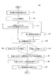
[0047]図2Aは、本発明の一実施形態の電界効果トランジスタのゲート誘電体を製造するために用いられる一連の方法ステップを含有するプロセス順序251を示す図である。プロセス順序251は、一般的には、例示的なMOSタイプデバイスのゲート構造を形成するために基板の上に行われる処理ステップを含む。図3A-図3Fは、ゲート酸化物層とゲートが図2Aに示したプロセス順序251におけるステップを用いて形成される基板401の領域を示す図である。図3A-図3Fの画像は、一定の比率で縮小して示されてなく、例示のために単純化されている。プロセス順序251の少なくとも一部は、図7に示したもののような統合した半導体基板処理システム(即ち、クラスタツール)における処理リアクタを用いて行うことができる。
[0047] FIG. 2A is a diagram illustrating a
[0048]プロセス順序251は、ステップ252から始まり、ステップ268に進む。ステップ252で、シリコン(Si)基板401(例えば200mmウエハ、300mm半導体ウエハ)を準備し、基板の表面から(図3A)から自然酸化物層401A(例えば、二酸化シリコン(SiO2))を除去するための洗浄液にさらす。一実施形態において、自然酸化物層401Aを、フッ化水素(HF)と脱イオン(DI)水を含む洗浄液を用いて除去する。一実施形態において、洗浄液は、約20〜約30℃の温度に維持される約0.1〜約10質量%のHFを含有する水溶液である。一例において、洗浄液は、約25℃の温度で維持される約0.5wt%のHFを含む。ステップ252で、基板401を洗浄液に浸漬することができ、その後、脱イオン水ですすぐことができる。ステップ252は、処理の間、超音波エネルギーの分配を含むことができる単一基板処理チャンバか又は複数基板バッチタイプ処理チャンバ内で行うことができる。或いは、ステップ252は、統合処理システム600(図7)の単一基板湿式洗浄リアクタを用いて行うこともできる。他の実施形態において、自然酸化物層401Aは、RCA洗浄法を用いて除去することができる。ステップ252の完了時に、基板401を真空ロードロック又は窒素(N2)でパージされた環境に入れる。或いは、ステップ252は、統合処理システム600(図7)の単一基板湿式洗浄リアクタを用いて行うことができる。
[0048] The
[0049]ステップ254で、熱酸化物(SiO2)層402を基板401(図3B)の洗浄した表面401B上で成長させる。一般に、熱酸化物層402の厚さは、約3〜約35オングストロームである。ロジックタイプの用途において、熱酸化物層402の厚さは、約6〜約15オングストロームであるのがよく、メモリタイプの用途において、熱酸化物層402厚さは、約15〜約40オングストロームであるのがよい。本発明の実施形態は、熱酸化物層の厚さが35オングストロームより大きくてもよい用途に用いることができる。熱酸化ステップ254によって、シリコン誘電体接合部上に形成する二酸化シリコン(SiO2)の副層が形成されることになる。ステップ254は、堆積される誘電体層(例えば、図3Dにおける高k誘電体層404)の上の誘電体/シリコン接合部の品質と信頼性を改善し、表面401Bの下のチャネル領域の電荷キャリヤの移動度も増大させると考えられる。ステップ254は、図7に示した統合処理システム600における基板処理チャンバ614A-614Fの一つに位置決めされた急速熱処理(RTP)リアクタを用いて行うことができる。一つの適切なRTPチャンバは、カリフォルニアのサンタクララのAppliedMaterials社から入手できるRADIANCE(登録商標)RTPチャンバである。一例において、6オングストローム二酸化シリコン(SiO2)膜は、酸素(O2)ガスの流量が2slmである18秒、750℃、2トールのプロセスを用いて基板401の表面401B上に形成される。この例において、熱酸化物層402の形成でプロセスチャンバに噴射される反応性ガスは酸素であるが、ある場合には不活性キャリヤガスをプロセスチャンバに加えて、所望のチャンバ圧を得ることができる。或いは、ある場合には、ステップ254で、一酸化窒素(NO)や亜酸化窒素(N2O)のような反応性ガス、又は水素(H2)/酸素(O2)や亜酸化窒素(N2O)/水素(H2)のような反応性ガス混合物を用いることが望ましいことがある。
[0049] At
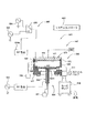
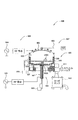
[0050]ステップ257で、高k誘電体層403を形成するのに望ましい物質で熱酸化物層をドープするために用いられる金属イオン含有プラズマに熱酸化物層402をさらす。ステップ257で形成される高k誘電体層403は、ハフニウム(Hf)、ランタン(La)又は他の同様の物質でドープされる二酸化シリコン層であるのがよい。一実施形態において、低エネルギー堆積プロセスは、以下で参照される、図4A-図4C及び図4Fによって記載されるチャンバと同様のプロセスチャンバを用いて行われる。一実施形態において、処理領域522に分配されたRFエネルギーを用いてプラズマを生成し、その後、ターゲット(例えば、図4Aの符号505又は図4Bの符号571)上にカソードバイアスを形成してそこからの物質をスパッタすることによってドーパント物質を熱酸化物層402に分配することが望ましい。一態様において、スパッタされた又はイオン化された物質を熱酸化物層402内の所望範囲の深さに注入させるために基板支持体562をRFバイアスにかけるか、DCバイアスにかけるか、又は接地することが望ましい。他の態様において、自己バイアスを生成するためにプラズマに相対して基板支持体562間に生じる電圧が、熱酸化物層402に衝撃するイオン化された物質のエネルギーを減少させるほど低いように基板支持体562を電気的に“浮遊させる”ことが望ましい。低エネルギー物質を分配して熱酸化物層402をドープする種々の方法は、図4A-図4F及び図5A-図5Cと共に以下に記載される。チャンバ圧、RF電力、パルスDC電力、基板支持体562に印加されたバイアス及び/又は処理時間の注意深い制御によって、熱酸化物層402におけるドーパント量とドーパント物質の濃度と深さとを制御することができる。一実施形態において、プラズマとしては、アルゴンイオンと、ハフニウムハフニウム、ランタン、アルミニウム、チタン、ジルコニウム、ストロンチウム、鉛、イットリウム、バリウムのような金属イオンを含有してもよいだけでなく、一つ以上の所望による不活性ガスを含有してもよい。典型的な不活性ガスとしては、ネオン(Ne)、ヘリウム(He)、クリプトン(Kr)、キセノン(Xe)、窒素(Ne)等が挙げられるのがよい。一例において、熱酸化物層402は、約5〜約30原子パーセント(原子%)のハフニウム(Hf)でドープされる。一般的には、熱酸化物層402及びシリコンチャネル表面(例えば、表面401B)との間の接合部の前に数オングストローム又は少なくとも数オングストロームのゼロ近くになるように、熱酸化物層402のドーパント濃度を低下させることが望ましい。一例において、処理チャンバ(図4Aにおける符号500)の誘導結合変形例を用いた場合、10原子%(平均)濃度のハフニウム(Hf)が、-150VDCをハフニウムターゲット(符号505)に印加し且つ“浮遊している”基板ペデスタルを用いて5%負荷サイクルを用いた13.56MHzの周波数と50ワットの電力でRFエネルギーをコイル(符号509)に分配する180秒と10ミリトールのチャンバ圧プロセス(例えば、主としてアルゴンガス)を用いて熱酸化物層402内に配置される。他の例において、図4Gに示されたものと同様のプロセス構成を用いた場合、7原子%濃度(平均)のハフニウム(Hf)が、約平均100ワットのRF電力(即ち、〜5%の負荷サイクルと〜2000WピークRF電力)をハフニウム含有ターゲット505に印加し且つ“浮遊している”基板ペデスタルを用いて13.56MHzの周波数で約100ワット平均RF電力(即ち、〜5%の負荷サイクルと〜2000WピークRF電力)をコイル509に印加する180秒と10ミリトールのチャンバ圧プロセス(主としてアルゴンガス)を用いて熱酸化物層内に配置される。一実施形態において、ステップ257で熱酸化物層402に対する損傷を防止するために、平均RF電力を約1000W未満のレベルに保持する。他の実施形態において、ステップ257で用いられる平均RF電力は、約200W未満である。他の実施形態において、更に、ステップ257で用いられる平均RF電力は、約50W未満である。一実施形態において、ステップ257は、図7に示した統合処理システム600における基板処理チャンバ614A-614Fの一つに位置決めされた低エネルギープラズマ処理チャンバ(例えば、処理チャンバ500又はプロセスチャンバ501)を用いて行われる。
[0050] In
[0051]一実施形態において、図2Aと図3Dに示されるように、ステップ254とステップ257を用いて熱酸化物層402から高k誘電体層403を形成する代わりに、金属有機化学気相堆積(MOCVD)プロセス、原子層堆積(ALD)プロセス又は他の同様の堆積プロセスを用いて基板401の表面401B上に高k誘電体層404を堆積させるために代替ステップ256を行うことができる。高k誘電体層404は、酸化ジルコニウム(ZrO2)、酸化ハフニウム(HfxOy)、ハフニウムシリケイトオキシド(HfxSi1-xOy)、酸化ランタン(La2O3)、及び/又は酸化アルミニウム(Al2O3)を含有するのがよいが、これらに限定されない。ステップ256は、例えば、AppliedMaterials社から入手できるCentura ALD High-Kシステムのような原子層堆積システムを用いて行うことができる。図7に示した統合処理システム600における基板処理チャンバ614A-614Fの一つにALDタイプリアクタを位置決めすることができる。
[0051] In one embodiment, as shown in FIGS. 2A and 3D, instead of using
[0052]ステップ259で、プラズマ堆積プロセスを行うことによって高k誘電体層403、或いは高k誘電体層404の表面を終了して、終端領域405を形成する。一般に、層物質を堆積させ及び/又は高k誘電体層403、又は高k誘電体層404をドープすることによって終端領域405を形成する。酸化ランタン(La2O3)又は酸化アルミニウム(Al2O3)のような不動態化物質を含有する終端領域405の添加は、表面を不動態化し、従来のALD又はMoCVD高k膜に一般に見られる問題、フェルミ準位ピンニング又は閾値電圧シフトを解決すると考えられる。一実施形態において、高k誘電体層403、又は高k誘電体層404は、約0.1〜約10原子%のランタン(La)、及び/又は約0.1〜約10原子%のアルミニウム(Al)でドープされる。他の実施形態において、高k誘電体層403、又は高k誘電体層404は、約0.25〜約5原子%のランタン(La)及び/又は約1〜約10原子%のアルミニウム(Al)でドープされる。高k誘電体層403又は高k誘電体層404のドーパント濃度を低下させることが望ましいので、高k誘電体層403、又は高k誘電体層404内に数オングストロームだけ広がると考えられる。一実施形態において、以下の図4A-図4Cに記載されるプロセスチャンバを用いてランタン(La)ドーパントを高k誘電体層403に入れる。一例において、-100VDCをランタンターゲット(例えば、図4Aにおける符号505)に適用し且つ“浮遊している”基板ペデスタルを用いて5%負荷サイクルを用いた13.56MHzの周波数と50Wの電力でRFエネルギーをコイルに分配する、120秒と10ミリトールのチャンバ圧プロセス(例えば、主にアルゴンガス)を用いた10原子%のハフニウムドープされた高k誘電体層403に0.5原子%(平均)濃度のランタン(La)を入れる。
[0052] At
[0053]一実施形態において、ステップ259は、図4A-図4Cに示した処理チャンバ500又はプロセスチャンバ501と同様のプロセスチャンバで行うことができる。この構成において、終端領域405は、ステップ257で上記プロセスと同様の、低エネルギー注入タイププロセスを行うことによって形成される。一態様において、処理領域522に分配されたRFエネルギーを用いてプラズマを生成し、その後、ターゲット505上にカソードバイアスを形成してそこから物質をスパッタすることよって、ドーパント物質を高k誘電体層403の上部のほとんどの領域に分配する。スパッタされイオン化された物質を高k誘電体層403に注入させるために、基板支持体562はRFバイアスをかけても、DCバイアスをかけても、接地されても、浮遊してもよい。低エネルギー物質を分配して高k誘電体層403をドープする種々の方法は、以下の図4A-図4Fと図5A-図5Cと共に後述される。それ故、チャンバ圧、RF電力、パルスDCバイアス、基板支持体562に印加される所望によるバイアス及び/又は処理時間を注意深く制御することによって、高k誘電体層におけるドーパント量とドーパント物質の濃度と深さを制御することができる。一実施形態において、ドーパントは、アルミニウム含有物質、ランタン含有物質、又は他の同様の物質である。
[0053] In one embodiment, step 259 may be performed in a process chamber similar to
[0054]一実施形態において、ステップ259は、図7に示した統合処理システム600の基板処理チャンバ614A-614Fの一つに位置決めされた処理チャンバ500を用いて行うことができる。一態様において、ステップ259を行うために用いられる処理チャンバ500は、ステップ257を行うために用いられるプロセスチャンバと異なる処理チャンバである。他の実施形態において、統合処理システム600に取り付けられている単一処理チャンバ500は、ステップ257とステップ259を行うために用いられるが、各ステップは、処理チャンバ500の処理領域522に配置される異なるターゲット物質を用いて行われる。
[0054] In one embodiment, step 259 may be performed using the
[0055]ステップ259の他の実施形態において、終端領域405は、スパッタリングプロセスを行うことにより高k誘電体層403の表面上に堆積される物質の追加の層であるのがよい。一態様において、スパッタリングプロセスは、図4A-図4Cに示した処理チャンバ500又はプロセスチャンバ501と同様のプロセスチャンバを用いて行われる。この構造において、終端領域405は、処理領域522へ分配されるRFエネルギーを用いてプラズマを生成させ、その後、ターゲット505上にカソードバイアスを形成して、そこから物質をスパッタすることにより、高k誘電体層403の最上部上にターゲット物質を堆積させることによって形成される。基板支持体562は、高k誘電体層403に注入するスパッタされイオン化された物質のエネルギーと深さを制御するためにRFバイアスがかけられても、接地されても、又は電気的に浮遊してもよい。一実施形態において、堆積された層は、アルミニウム(Al)、ランタン(La)、又は他の適切な物質を含有する。
[0055] In other embodiments of
[0056]一実施形態において、所望によるステップ260は、酸素含有RFプラズマを用いて、さらされた物質を酸化して、それらを誘電体物質に変換する。一例において、高k誘電体層403、高k誘電体層404及び/又は終端領域405は、酸素含有プラズマにさらして、酸化アルミニウム又は酸化ランタンを形成する。他の実施形態において、プラズマは、窒素(N2)を含有し、O2、NO、N2Oのような一つ以上の酸化ガスを含有してもよい。プラズマは、また、アルゴン(Ar)やヘリウム(He)のような一つ以上の所望による不活性ガスを含有してもよい。ステップ260は、例えば、統合処理システム600(図7)の減結合プラズマ窒化(DPN)プラズマリアクタを用いて行うことができる。一実施形態において、プラズマ酸化ステップの代わりに熱酸化ステップを用いて、さらされた物質を酸化して、それを誘電物質に変換する。一例において、プラズマ酸化プロセスは、さらされた物質を酸化させるために、約100sccmの窒素流量と約100sccmの酸素流量を用いて5%の負荷サイクルと1000Wピーク電力(即ち、平均電力50W)を13.56MHzのRF周波数で30秒間用いて行われる。
[0056] In one embodiment, the
[0057]一代替的実施形態において、所望によるステップ262は、ステップ260の代わりに用いられる。ステップ262において、高k誘電体層403、又は高k誘電体層404と、基板401は、約600℃〜1100℃の間の温度でアニールされる。約600℃〜800℃の温度で行われるアニールのようなより低い温度のアニールは、ハフニウムとシリコン(Si)、酸素(O2)、又はそれらの双方とのような前に堆積された物質の結晶化を防止するために有利に用いることができる。ステップ262は、統合処理システム600のRADIANCE(登録商標)又はRTPXE+リアクタのような適切な熱アニールチャンバ、又は単一基板炉或いはバッチ炉を用いて行うことができる。ステップ262により、高k誘電体層403又は終端領域405にシリケートサブレイヤーが形成される。一実施形態において、ステップ262は、約600℃〜約1100℃の基板表面温度と、約0.1〜約50トールのプロセスチャンバ圧を維持しつつ、約2〜約5000sccmの酸素(O2)と約100〜約5000sccmの一酸化窒化(NO)の少なくとも一つを供給することよって行われ、所望によりいずれのガスも窒素(N2)と混合されてもよい。プロセスは、約5-180秒間行うことができる。一例において、ステップ262は、60sccmの流量の酸素(O2)ガスと940sccmの流量の窒素(N2)ガスを持つ、15秒、900℃、1トールプロセスである。他の例において、約1000℃の温度と約1トールの圧力で約15秒間プロセスチャンバを維持しつつ、O2を約200sccm(例えば、約200mTの酸素分圧)で供給し、窒素(N2)を約800sccmで供給する。更に他の例において、NOは、チャンバを約1000℃の温度と約0.5トールの圧力で約15秒間維持しつつ、約500sccmで供給される。
[0057] In an alternative embodiment,
[0058]一実施形態において、ステップ256、257、又は259のいずれかを行った後、ステップ260又は262はいずれも行われない。プロセス順序251の一実施形態において、ステップ260又は259と同様の酸化ステップは、終端領域405が高k誘電体層403の上に堆積される前に、ステップ257で堆積されたドーパント物質を再酸化するために、ステップ257と259の間で行うことができる。
[0058] In one embodiment, after performing any of
[0059]ステップ264で終端領域405と高k誘電体層403、又は高k誘電体層404は、これらの領域における窒素量を増やすために窒素プラズマ中で処理される。プロセスは、約10〜約2000sccmの窒素(N2)、約20〜約500℃の基板ペデスタル温度、約5〜約200ミリトールの反応チャンバの圧力を与えることによって、DNPリアクタを用いて行うことができる。高周波(RF)プラズマは、例えば、約13.56MHz又は60MHzで、連続波(CW)か又は約3〜5kWまでのパルスプラズマ電源を用いて励起される。パルスの間、ピークRF電力、周波数、負荷サイクルは、典型的には、それぞれ、約10〜3000W、約10kHz、2%〜100%の範囲で選択される。このプロセスは、約1秒〜180秒間行うことができる。一例において、N2は、約200sccmで供給され、約1000WのピークRF電力は、約10kHzで約5%の負荷サイクルでパルスされ、約25℃の温度と約10〜約80ミリトールの圧力で15秒〜180秒間誘導性プラズマソースに印加される。プラズマは、他のプラズマソースの中で、準遠隔プラズマソース、誘導性プラズマソース、又はラジアルラインスロットアンテナ(RLSA)ソースを用いて生成される。代替的実施形態において、CW及び/又はマイクロ波電力ソースを用いて、窒素含量が高い領域を形成することができる。
[0059] In
[0060]ステップ266で、基板401は、基板401上に形成される層の間の漏れ電流を減少させるためにアニールすることができ、表面401Bの下のチャネル領域における電荷キャリヤの移動度を増大させるだけでなく、形成されたデバイスの信頼性が改善される。ステップ266は、基板401上に形成される層内の欠陥の数を減少させることを援助し得る。ステップ266でステップ264において形成された窒化層をアニールするか又は不活性化する作用もまた、ホウ素ドープされた多結晶シリコンゲート電極からのホウ素の拡散に対する有効なバリアの形成を促進することを援助する。ステップ266は、統合処理システム600のRADIANCE(登録商標)又はRTPXE(登録商標)リアクタのような適切な熱アニールチャンバ、又は単一基板炉或いはバッチ炉を用いて行うことができる。一実施形態において、ステップ266のアニールプロセスは、約800℃〜約1100℃の基板表面温度と、約0.1〜約50トールの反応チャンバの圧力を維持しつつ、約2〜約5000sccmの流量の酸素(O2)と約100〜約5000sccmの流量の一酸化窒素(NO)の少なくとも一つを供給することによって行うことができ、所望によりガスを窒素(N2)と混合してもよい。プロセスは、約5-180秒間行われるのがよい。一実施形態において、酸素(O2)ガスは、約1000℃の温度と約0.1トールの圧力で約15秒間維持しつつ、約500sccmで供給される。一実施形態において、ステップ266は、上記ステップ262に用いられたものと同様のプロセス法を用いる。
[0060] At
[0061]ステップ260、262、264又は266の完了時に、形成された層の上に一つ以上の層が堆積されて、ステップ268を用いて形成されたMOSデバイスのゲート領域、又はゲート電極を形成する。ステップ268の一実施形態において、多結晶シリコン層は、ゲート電極を提供するために上記層の上のゲート領域に堆積される。一例において、多結晶シリコン層は、従来の多結晶シリコン堆積プロセスを用いて堆積される。一実施形態において、多結晶シリコン堆積チャンバ(図示せず)は、統合処理システム600の一部である。一実施形態において、多結晶シリコンは、図7に示される統合処理システム600の基板処理チャンバ614A-614Fの一つを備える、AppliedMaterials社から入手できるCentura CVDリアクタのようなCVD又はALDリアクタを用いてプロセス順序251で形成された層の上に堆積される。
[0061] Upon completion of
[0062]ステップ268の他の実施形態において、図3Fに示したように、ゲート領域408は、薄い金属層407と多結晶シリコン層406のような複数の導電層を含有する。一実施形態において、ゲート領域408は、従来の多結晶シリコンゲート物質より高いキャリヤ濃度を持つゲート物質を提供するためのプロセス順序251で形成された層の上に堆積される薄い金属層407を含有する。薄い金属層407は、約5〜約200オングストロームの厚さを持つのがよい。一実施形態において、薄い金属層407は、タンタル(Ta)、窒化タンタル(TaN)、炭化ランタン(LaC)、タングステン(W)、窒化タングステン(WN)、窒化シリコンタンタル(TaSiN)、ハフニウム(Hf)、アルミニウム(Al)、ルテニウム(Ru)、コバルト(Co)、チタン(Ti)、ニッケル(Ni)、窒化アルミニウムチタン(TiAlN)、窒化ルテニウム(RuN)、窒化ハフニウム(HfN)、ケイ化ニッケル(NiSi)、窒化チタン(TiN)又は他の適切な物質のような金属を含有する。薄い金属層407は、図7に示した統合処理システム600に取り付けられている処理チャンバ500(図4A)又はプロセスチャンバ501(図4B-図4C)を用いて有利に形成することができる。この構成において、薄い金属層407は、RFエネルギーを用いてプラズマを生成し、ターゲットにバイアスをかけてそこからの金属をスパッタし、その後、所望により基板支持体562(図4A-4B)にバイアスをかけてもよく、スパッタされイオン化された金属物質をあらかじめ形成された層の上に堆積させることによりプロセス順序251で形成された層の上にターゲット物質を堆積させることによって形成される。スパッタ堆積プロセスを動かすためのRFエネルギーの使用は、非常に少量の物質を基板表面上に確実に堆積させることを可能にする。反対に、薄い金属層を形成するのに充分低いレベルまで堆積速度を低下させるのに必要とされるスパッタリング(DC)電圧の印加が、通常はスパッタリングプラズマを持続しないので、従来の物理気相堆積、又はスパッタリング技術は、薄い物質層を確実に堆積させる能力が大幅に制限される。他の実施形態において、薄い金属層407は、従来のCVD、PECVD又はALDプロセスを用いて形成することができる。
[0062] In another embodiment of
[0063]図2Bは、プロセス順序251の他の実施形態を示す図である。図2Bに示したプロセス順序251は、二つの所望によるステップ258A及び/又は258Bの少なくとも一つがステップ257、又はステップ256とステップ259の間に加えられる以外は、図2Aに示された方法のステップと同じである。一実施形態において、ステップ254、256又は257の一つで形成された高k誘電体層403、又は高k誘電体層404に見られる物質の一つ以上を窒化するためにプラズマ窒化ステップがプロセス順序251に加えられる。一例において、ステップ258B、262、又は266のような続いてのアニールステップで、高k誘電体層403、又は高k誘電体層404に見られるハフニウム物質の結晶化を防止するためにプラズマ窒化プロセスを用いて窒化ハフニウム含有層を形成することは望ましいことである。一実施形態において、ステップ258Aは、ステップ264と共に本明細書に記載されるプロセスを用いて行われる。
[0063] FIG. 2B illustrates another embodiment of a
[0064]一実施形態において、所望による熱アニールステップ、ステップ258Bは、形成された高k誘電体層403又は高k誘電体層404における欠陥や応力を減少させて形成されたデバイスの信頼性を改善するためにプロセス順序251に加えられる。一実施形態において、ステップ258Bは、ステップ262及び/又はステップ266と共に本明細書に記載されるプロセスを用いて行われる。一実施形態において、ステップ258Bは、上記ステップ258Aを行った後に終了する。一例において、ステップ258Bは、酸素(O2)ガスの流量が60sccmで窒素(N2)ガスの流量が940sccmである、15秒、900℃、1トールのプロセスである。
[0064] In one embodiment, the optional thermal annealing step,
[0065]図2Cは、プロセス順序251の他の実施形態を示す図である。図2Cに示したプロセス順序251は、ステップ253がステップ252とステップ254の間に加えられ、ステップ256がステップ254の後に行われる以外は図2Aに示したステップと同じである。この実施形態において、プラズマ窒化ステップ、ステップ253を、ステップ252で自然酸化物層を除去した後にプロセス順序251に加えて、ステップ254又はステップ256を行う前に基板表面を窒化する。窒化されたシリコン基板表面は、続いての熱酸化ステップ(ステップ254)で形成される酸化シリコン層の表面に又は酸化シリコン層の近くに残る望ましい酸窒化シリコン(SiON)を形成することを援助すると考えられる。形成された二酸化シリコン層の表面に又は二酸化シリコン層の近くに残るSiON層の形成は、続いてのプロセスステップでゲート電極物質(ステップ268)のゲート誘電体層への拡散を最小にすることを援助することができる。ステップ256と254がこの実施形態で行われる順序は、ステップ256を用いて高k誘電体層を堆積させる前に酸窒化シリコン(SiON)接合層を形成することを可能にするために変更し、高k誘電体層とデバイスのチャネル領域の間の接合部の特性を改善することを援助する。ステップ253は、カリフォルニアのサンタクララのAppliedMaterials社から入手できるDPNリアクタで行うことができる。一例において、ステップ253は、25W平均RF電力(500WピークRF電力の5%負荷サイクル)、N2の200sccmのガス流量、25℃の基板温度を用いて、10秒、70ミリトールプロセスを用いる。また、プロセス順序251の一実施形態において、ステップ254は、ステップ253で行われた窒化されたシリコン表面の望ましい特質が保持されることを確実にするように変えられる。この場合、高品質誘電体膜が形成されることを確実にするためにステップ254で酸素と共に窒素(N2)のような他の反応性ガスをプロセスチャンバに噴射することは望ましいことである。一例において、酸窒化シリコン(SiON)膜は、15sccmの流量の酸素(O2)ガスと、5slm流量の窒素(N2)ガスを持つ30秒、1050℃、5トール(即ち、15ミリトールの酸素分圧)のプロセスに続いて、0.5slm流量の酸素(O2)ガスと4.5slm流量の窒素(N2)ガスを15秒間の変更ガス設定を用いて表面401B上に形成される。
[0065] FIG. 2C is a diagram illustrating another embodiment of a
[0066]図2Dは、プロセス順序251の他の実施形態を示す図である。図2Dに示したプロセス順序251は、二つの所望によるステップ255A又はステップ255Bがステップ254と257の間に加えることができる以外は、図2Aに示したステップと同じである。一実施形態において、所望によるプラズマ窒化ステップ、ステップ255Aをステップ254とステップ257の間に加え、ステップ254で形成された熱酸化物層の最上面を窒化して、SiON層を形成する。SiON層は、ゲート電極物質がゲート誘電体層に拡散することを防止する拡散バリヤとして作用することができる。一例において、ステップ255Aは、50W平均RF電力(1000WピークのRF電力の5%の負荷サイクル)、N2の200sccmのガス流量、約25℃の基板温度を用いる30秒、10ミリトールプロセスを用いる。
[0066] FIG. 2D is a diagram illustrating another embodiment of a
[0067]図2Dを参照すると、一実施形態において、所望による熱アニールステップ、ステップ255Bをプロセス順序251に加えて、形成された高k誘電体層403の欠陥と応力を減少させて、形成されたデバイスの信頼性を改善する。一例において、ステップ255Bのアニールプロセスは、約1050℃の基板温度と、約1〜約5トールの反応チャンバの圧力を維持しつつ、約15sccmの流量の酸素(O2)と約500sccmの流量の窒素(N2)の少なくとも一つを供給することによって行うことができる。他の実施形態において、ステップ255Bは、ステップ262及び/又はステップ266と共に本明細書に記載されたプロセスを用いて行われる。一実施形態において、ステップ255Bは、上記ステップ255を行った後に完了する。
[0067] Referring to FIG. 2D, in one embodiment, an optional thermal annealing step, step 255B, is added to the
[0068]図2Eは、プロセス順序251の他の実施形態を示す図である。図2Eに示したプロセス順序251は、ステップ254が除去され、ステップ252を変更して(新しいステップ252A)、湿式洗浄プロセスが酸化シリコン含有接合層を形成することを可能にする以外、図2Aに示したステップと同じである。この実施形態において、新しいステップ252Aは、洗浄し、湿式洗浄プロセスを用いて基板の表面401B上に酸化物層を意図的に形成する。新しいステップ252Aは、カリフォルニア、サンタクララのAppliedMaterials社から入手できるEmerisonTMチャンバ内で行うことができる。一例において、4〜5オングストロームの酸化物層は、ステップ252Aで、基板を希フッ化水素酸(HF)浴に8分間浸漬し、その後、50℃で6分間維持される標準洗浄1(SC1)浴(例えば、<5容積%の水酸化アンモニウム(NH4OH)/<3容積%の過酸化水素(H2O2)/残量のDI水)内で洗浄し浸漬し、その後、基板をDI水を含有するメガソニック作動タンク(即ち、1500W)内で所望される時間すすぐことにより形成される。他の例において、酸化物層は、オゾン(O3)含有洗浄液を用いる湿式洗浄プロセスによって形成することができる。
[0068] FIG. 2E is a diagram illustrating another embodiment of a
[0069]図2Fは、プロセス順序251の他の実施形態を示す図である。図2Fに示したプロセス順序251は、ステップ256がステップ254の後に行われる以外、図2Aに示したステップと同じである。この実施形態において、ステップ256とステップ254が行われる順序は、ステップ256で薄い二酸化シリコン(SiO2)層(例えば、<10オングストローム)が高k誘電体層を堆積する前に形成されることを可能にするように変更されている。一実施形態において、薄い高k誘電体層404は、ALDタイプの堆積プロセスを用いて、ステップ254で成長する熱酸化物層402上に堆積させる。この構成は、完全なスタックの望ましい誘電特性を示しつつ、ステップ254で形成された薄い二酸化シリコン層がデバイスの誘電体層とチャネル領域の間の接合で良好な誘電体/チャネル領域接合部を与えるので有用であると考えられる。
[0069] FIG. 2F illustrates another embodiment of a
設計のハードウエア態様
[0070]上述したように、上記ステップ257とステップ259と共に記載されたプラズマ処理プロセスを用いて高k誘電体層を形成することは望ましい。大きなプラズマ電位、例えば、数十ボルト程度で用いるプラズマプロセスは、薄いゲート誘電体層に対する損傷を引き起こし、衝撃金属原子が形成されたMOSデバイスの下に横たわるチャネル領域に混入することさえ引き起こし得る。二酸化シリコンのような誘電体層に対する損傷又は金属原子の下に横たわる領域への混入は、デバイス性能の低下と漏れ電流の増加のために望ましくない。下記の種々の実施形態は、プラズマ処理プロセスを用いてゲート誘電体層を確実に形成するために使用し得る。このような金属プラズマ処理を行うために用いることができる種々の装置の例は、図4A-4Cと図4Fと共に以下に記載する。
Hardware aspects of design
[0070] As noted above, it is desirable to form a high-k dielectric layer using the plasma processing process described in conjunction with
誘導結合プラズマ処理チャンバ
[0071]図4Aは、上記ステップ257及び/又は259のプロセスを行うために使用し得るプラズマ処理チャンバ500の一実施形態の概略断面図を示す図である。この構成において、処理チャンバ500は、処理領域522において、基板401(図3A)のような基板502を処理することができる誘導結合プラズマ処理チャンバである。一実施形態において、処理チャンバ500は、誘導結合RFソースを用いる、サンタクララのAppliedMaterials社から入手できる変更されたプラズマ窒化(DPN)チャンバである。
Inductively coupled plasma processing chamber
[0071] FIG. 4A shows a schematic cross-sectional view of one embodiment of a
[0072]処理チャンバ500は、通常は、誘導RFソースアセンブリ591、DCソースアセンブリ592、ターゲット505、システムコントローラ602、プロセスチャンバアセンブリ593、及び基板支持アセンブリ594を含有する。プロセスチャンバアセンブリ593は、通常は、プラズマプロセスがその中で行うことができるように処理領域522内に真空を形成し得る要素を含有する。一般に、プロセスチャンバアセンブリ593は、処理領域522を密封するチャンバベース527とチャンバ壁528とチャンバリッド529を含有する。処理領域522は、チャンバベース527及び/又はチャンバ壁528を通って処理領域522に接続される真空ポンプ510の使用によって所望の真空圧に排気され得る。一般に、チャンバ壁528とチャンバベース527は、アルミニウム、又は他の適切な物質のような金属から形成することができる。一実施形態において、チャンバ壁528は、ターゲット505からスパッタされた物質がチャンバ壁528上に載ることを防止する取り外し可能なチャンバシールド(図示せず)を持つことができる。
[0072] The
[0073]誘導RFソースアセンブリ591は、通常は、チャンバリッド529に隣接して位置決めされているコイル509に接続されるRFジェネレータ508とRF整合508Aを含有する。一実施形態において、RFジェネレータ508は、約0〜約3000Wで、約400kHz〜約20MHzの周波数で作動させることができる。一例において、RFジェネレータ508は、13.56MHzの周波数で動作させる。チャンバリッド529は、通常は、誘導RFソースアセンブリ591から分配されるRFエネルギーが処理領域522でプラズマを形成するように適応される誘電体要素(例えば、石英、セラミック物質)である。一実施形態において、コイル509は、処理領域522に生成されるプラズマがスパッタプロセスでターゲットの活性面の近くに形成されるようにターゲット505の近くに位置決めすることができる。活性表面の近くのプラズマの制御は、低エネルギースパッタ堆積プロセスの間でスパッタされるターゲットの領域の近くのプラズマ密度を制御することを援助することができる。この構成は、コイル509によって生成されたプラズマのために、極端に薄いゲート誘電体層の望まれていないプラズマ衝撃の量を減少させるのに有用なものである。
[0073] Inductive
[0074]一実施形態において、チャンバリッド529は、真空シールされた電気的フィードスルー504が処理領域に位置決めされているターゲット505と接触させることを可能にするように変更される。この構成において、同軸ケーブル506を真空シールされたフィードスルー504に接続して、エネルギーをDC電源507から分配して、プラズマに生成したイオンが物質をターゲットから基板502にスパッタさせる。図5A-図5Cと共に以下に記載される一態様において、システムコントローラ602は、RFジェネレータ508からの出力とDCソース592アセンブリから分配されるDC電力を同期させるために用いられる。一実施形態において、ターゲット505は純粋な物質又はハフニウム(Hf)、ランタン(La)、アルミニウム(Al)、チタン(Ti)、ジルコニウム(Zr)、ストロンチウム(Sr)、鉛(Pb)、イットリウム(Y)、又はバリウム(Ba)のグループより選択される元素を含有する合金から形成することができる。
[0074] In one embodiment, the
[0075]一態様において、プロセスチャンバアセンブリ593は、また、チャンバベース527とチャンバ壁528とチャンバリッド529によって形成された処理領域522に一つ以上のプロセスガスを分配するように適合されたガス分配システム550を含有する。処理領域522の圧力は、ガス分配システム550とスロットバルブ511によって調節される真空ポンプ510のポンピング速度によって分配されたガス流量を調整するために用いられるシステムコントローラ602の使用によって制御され得る。一態様において、処理中のチャンバ圧は、約5ミリトール〜約100ミリトールである。
[0075] In one aspect, the
[0076]基板支持アセンブリ594は、通常は、基板支持部材562Aを含有する基板支持体562を含む。基板支持部材562Aは、基板を処理中に活発に保持するために使用し得る慣用の静電チャックであっても簡単な基板支持ペデスタルであってもよい。温度コントローラ561は、通常は、熱交換機(図示せず)に結合される埋め込まれた抵抗加熱素子又は流体冷却チャネルのような慣用の手段の使用による温度コントローラ561によって所望の温度設定に基板支持部材562Aを加熱及び/又は冷却するように適合される。一態様において、温度コントローラ561は、動作させ、基板支持部材562A上に位置決めされた約20℃〜約800℃の温度に加熱するように適合される。処理の間、基板支持体562は、処理領域522において基板502の表面に生成されたプラズマ内に有するイオンを引っぱるための基板支持体562の部分にRFバイアスが印加され得るようにRFジェネレータに接続するのがよい。一実施形態において、基板支持部材562Aは、基板502のイオン衝撃損傷を最小にするためにプラズマプロセスの間、接地されるか、DCバイアスをかけるか、又は電気的に浮遊している。
[0076] The
[0077]RFエネルギーをRFジェネレータ508から処理領域522に分配すると、イオン化される処理領域においてガス原子を生じる。その後、プラズマ内のイオン化された原子は、物質がターゲット505からスパッタされるとともに基板502の表面に載ることができるようにDCソースアセンブリ592によってターゲット505に印加されたカソードバイアスのためにターゲット505に引きつけられる。誘導RFソースアセンブリ591から分配されたRFエネルギーとDCソースアセンブリ592から印加されたDCバイアスの干渉と相互作用を減少させる努力において、干渉が最小であり、堆積速度、膜均一性、膜質が最大にされたときに最小化できるように、DCソースアセンブリ592及びRFソースアセンブリ591から分配されたエネルギーパルスを同期することがしばしば望ましい。プラズマを励起するために誘導RFソースをパルスすると、低電子温度と、低エネルギープラズマを生成し維持することによって基板の表面に対する損傷を引き起こす高プラズマ電位と関連した問題を改善する。一般に、パルスRF誘導プラズマによって生成されるイオンは、プラズマ内に位置決めされた基板を損傷しない低イオンエネルギー(例えば、<10eV)でイオンを得る。このことは、2003年6月12日出願の共同譲渡された米国特許第6,831,021号により完全に記載され、この開示内容は本明細書に援用されている。アルゴン(Ar)、ネオン(Ne)、クリプトン(Kr)、又はキセノン(Xe)のようなほとんどの不活性ガスの低イオンエネルギーは、ハフニウム(Hf)、ランタン(La)又は他の重金属又は誘電物質から製造されるターゲットから原子をスパッタするほどパルスRFソースから充分なエネルギーを得ない。例えば、アルゴンプラズマについては、HfとLaターゲットのスパッタリング閾値エネルギーは、それぞれ42.3eVと25.5eVであり、ゲート酸化物へのイオン注入の安全なイオンエネルギーは、通常は10eV未満である。つまり、RF誘導プラズマについて、ゲート誘電体層の形成するのに安全である充分低いイオンエネルギーは、ターゲット物質から所望の金属イオンをスパッタするほど充分高くない。それ故、スパッタリングプロセスを行うためのDCソースアセンブリ592からターゲットに印加したDCバイアスを用いることが求められている。種々のパルス堆積プロセスの様態を、図5A-図5Cと共に以下に記載する。
[0077] Distributing RF energy from the
容量結合プラズマ処理チャンバ
[0078]図4B-図4Cは、上記ステップ257及び/又は259に記載したプロセスを行うために使用し得るプラズマ処理チャンバの他の実施形態の概略断面図を示す図である。この構成において、プロセスチャンバ501は、処理領域522において基板502を処理することができる容量結合プラズマ処理チャンバである。プロセスチャンバ501は、通常は、VHFソースアセンブリ595と、ターゲットアセンブリ573と、システムコントローラ602と、プロセスチャンバアセンブリ596と、基板支持アセンブリ594とを含有する。この構成において、容量結合プラズマは、ターゲット571に接続されるVHFソースアセンブリ595の使用によってプロセスチャンバアセンブリ596内に含有するターゲット571と接地チャンバ壁528との間の処理領域522に形成される。プロセスアセンブリ596は、通常は、チャンバリッド529をチャンバ壁528上に密封して位置決めされるターゲットアセンブリ573と電気絶縁体572に置き換えた以外は、上の図4Aと共に記載された要素のすべてを含有する。プロセスチャンバアセンブリ596及び基板支持アセンブリ594内の要素は、処理チャンバ500によって記載されものと同一か又は同様のものであり、そのように、適切な場合には同様の符号を用い、下で繰り返さない。
Capacitively coupled plasma processing chamber
[0078] FIGS. 4B-4C are schematic cross-sectional views of other embodiments of plasma processing chambers that may be used to perform the process described in
[0079]図4Bを参照すると、一実施形態において、VHFソースアセンブリ595は、ターゲットアセンブリ573の一つ以上の部分を通って処理領域522にRFエネルギーを分配するように適合されるRFソース524と整合524Aを含有する。ターゲットアセンブリ573は、通常は、バッキングプレートアセンブリ570とターゲット571を含有する。バッキングプレート570は、プロセス中の熱交換器(図示せず)とターゲット物質の充分な使用を促進するとともに堆積均一性を高めるように適合されるマグネトロンアセンブリ(図示せず)から分配された流体へターゲットを冷却する流体チャネル(図示せず)を含有してもよい。
[0079] Referring to FIG. 4B, in one embodiment, the
[0080]プロセスチャンバ501の動作中、VHFソースアセンブリ595は、ターゲット571が形成される物質内の原子が基板502の表面上に堆積され得るようにターゲット571にバイアスをかけるために用いられる。一実施形態において、VHFソースアセンブリ595内のRFソース524は、約1〜約200MHzのRF周波数で約0.01〜約5キロワット(kW)の電力でターゲットアセンブリ573を通って処理領域522に電力を分配するように適合される。一実施形態において、プラズマによって生成されたイオンがターゲット571の表面から物質をスパッタさせるプラズマシース全体の電圧低下のために、VHFソースアセンブリ595を用いて、充分なエネルギーを供給する容量結合ターゲット571上に自己バイアスを生成させる。VHFソースを用いてバイアスがかけられる容量結合電極、又はターゲットは、通常は、アノードとカソード(例えば、ターゲット571)の表面積の差のために、自己バイアス電圧に達する。ターゲット571が処理中に達する自己バイアス電圧は、ターゲット571のスパッタ速度を最適化するように調整され得る。図4Eは、自己バイアス電圧と周波数とのグラフを示す図である。グラフは、通常は、次第により高い周波数でバイアスがかけられたときの電極の自己バイアス電圧に対する周波数の影響を示している。周波数が増加するにつれて自己バイアス電圧の大きさが減少する傾向ので、VHFソースアセンブリ595の周波数が増加することによってターゲットに衝突するイオンのエネルギーが減少され得る。例えば、27MHzの周波数でRF信号を用いてバイアスがかけられるターゲットは、アルゴンを用いて50ミリトールの圧力と300WのRF電力でわずかに約10Vの電圧を持つ。他の例において、ターゲット上のDCバイアスは、約400Wの一定のRF電力を用いて約60MHz〜約100MHzのRF周波数を変動させることによって約-50V〜約-20Vに変動させ得る。
[0080] During operation of the
[0081]VHF範囲のRF周波数でターゲット571にエネルギーを分配すると、ターゲット571に分配される周波数の変動とRF電力の変動の関数としてターゲット上のDCバイアスの変動が減少するために、より低いRF周波数で行われるプロセスに対してステップ257及び/又は259のプロセス結果が改善され得る。DCバイアスの変動を減少させることは、低電力スパッタリング動作を行う場合に重要であり得る。それ故、RFエネルギーと電力の周波数の制御することによって、例えば、所望の負荷サイクル(下記)でターゲット571に電力を分配することによって、ターゲットのDCバイアスが正確に且つ繰り返して行うことができる。DCバイアスの正確で精密な制御は、極端に薄いゲート誘電体層をドープするプロセスが正確に且つ繰り返し行われ得ることを確実にする。
[0081] Distributing energy to the
[0082]図4Dを参照すると、一例において、スパッタリングガスが主としてアルゴン(Ar)であり、ターゲットがランタン(La)から製造される場合には、ターゲット表面からランタン原子をスパッタするのに必要とされるエネルギーは、少なくとも25.5eVである。このことは、ランタン原子の一部がターゲット表面からスパッタされることを確実にするためにターゲット上に生じた自己バイアス電圧が約25.5eVのイオンエネルギーを生成するのに充分高いことが必要であることを意味する。それ故、ターゲット571に分配される周波数と電力(例えば、ワット)を制御することによって、スパッタ速度、ガス原子イオンエネルギー、スパッタ原子のイオンエネルギー、基板上に堆積される原子のエネルギーが制御され得る。また、プロセスの間、基板支持体562に対するバイアスは、スパッタされた原子が、ゲート誘電体層上に堆積するか又はゲート誘電体層内に注入するのにつれて持つエネルギーを制御するために調整され得る。
[0082] Referring to FIG. 4D, in one example, when the sputtering gas is primarily argon (Ar) and the target is made from lanthanum (La), it is required to sputter lanthanum atoms from the target surface. The energy is at least 25.5 eV. This requires that the self-bias voltage generated on the target is high enough to produce ion energy of about 25.5 eV to ensure that some of the lanthanum atoms are sputtered from the target surface. It means that there is. Therefore, by controlling the frequency and power (eg, watts) distributed to the
[0083]一般に、スパッタプロセスは、約1sccm〜約500sccmのアルゴン流量を用いた1ミリトール〜100ミリトールの範囲のチャンバ圧と約20℃〜約800℃のヒータ温度でプロセスチャンバ501内で行うことができる。望ましくは、基板温度は、約200℃〜300℃である。RFソース254の励起周波数は、ターゲット物質がプラズマに、また、基板表面にスパッタさせる正しい自己バイアスDC電圧を得るために約1MHz〜約200MHzに調整され得る。好ましくは、RFソース254の励起周波数は、約27MHz〜約100MHzの周波数、より好ましくは約30MHz〜約60MHzの周波数に調整され得る。一例において、ランタンターゲットの場合、60MHzの周波数が所望のスパッタリングエネルギーと低エネルギープラズマを維持することを得るように選択され得る。一実施形態において、基板502の表面とターゲット571の表面との間の空間を調整して、基板表面上に堆積するスパッタされた原子の均一性とエネルギーを調整することは望ましいものである。一態様において、堆積プロセス中にターゲット571の表面に相対して基板502の空間を調整して、ゲート酸化物層のスパッタ物質の深さを及び/又は堆積均一性を調整することは望ましいものである。
[0083] Generally, the sputter process is performed in the
[0084]図4Cは、プロセスチャンバ501の第二実施形態を示す図であり、図4Bに示したVHFソースアセンブリ595が、プロセス中に異なる時間で異なるスパッタリング特性を与える異なる周波数及び/又は電力でプロセスチャンバ501の処理領域522にエネルギーを分配するようにそれぞれ適合される二つのRFジェネレータ524、525を含有するデュアルVHFソースアセンブリ597に置き換えられている。図4Cに示したプロセスチャンバ501は、通常は、ターゲットアセンブリ573に接続されたRFソース524と、第二RFソース525と、RFスイッチ526と、整合524Aを含有する。この構成において、デュアルVHFソースアセンブリ597からのターゲットアセンブリ573に分配されるエネルギーは、RFスイッチ526の使用によってRFソース524と第二RFソース525との間でスイッチが切り替えられ得る。スイッチ526の状態は、システムコントローラ602によって制御される。この実施形態は、最初の導入の間又は長いアイドルタイムの後にターゲット基板上に形成することができる酸化物を除去するために高速開始シージングを必要とするターゲット物質に有用なものである。より低い周波数ソース(例えば、約27MHz以下)にスイッチを切り替える能力は、高自己バイアスDC電圧がターゲット571上に形成することを可能にし、より高速なターゲットスパッタリング速度につながる。従って、開始処理後、高い周波数(約60MHz)ソースにスイッチを切り替えてスパッタリング速度を減少させ、且つスパッタされた原子イオンエネルギーを小さくすることによって、デュアルVHFソースアッセンブリ597の出力を変化させることができるので、基板表面上のゲート誘電体層に対する潜在的損傷が減少する。一例において、RFソース524は、約27MHzの周波数で0〜約2000ワットの電力でのRFエネルギーを分配することができ、第二のRFソース525は、約40〜約200MHzの周波数において0〜約500ワットの電力でRFエネルギーで分配することができる。
[0084] FIG. 4C is a diagram illustrating a second embodiment of the
[0085]一実施形態において、DCソースアッセンブリ592は、任意により、ターゲットアセンブリ573に接続してプラズマ処理ステップで一つ以上のDCエネルギーパルスを分配してもよい。DCバイアスを、VHFソースアセンブリ(例えば、符号595と597)から分配されたVHF信号の上に重ね合わせてもよい。ターゲット571に印加されるDC電圧は、スパッタリングプロセスでターゲット571に衝突するイオン化されたガス原子のエネルギーをより直接制御するために使用し得る。
[0085] In one embodiment, the
[0086]一実施形態において、上記のように、処理の間、RF、又はVHF、バイアスが、プラズマ内に存在するイオンを基板502の表面に引っ張るために基板支持体562の一部に印加され得るように基板支持体562をRFジェネレータ523に接続することができる。一実施形態において、基板支持部材562Aは、基板502のイオン衝撃損傷を最小にするためにプラズマプロセスの間、接地されるか、DCバイアスがかけられるか、又は電気的に浮遊している。
[0086] In one embodiment, as described above, during processing, RF, or VHF, bias is applied to a portion of the
パルスプラズマ処理
[0087]図5A-図5Cは、上記ステップ257及び/又は259で図4Aに示したターゲット505、又は図4Bに示したターゲット571から基板502の表面に、スパッタされた物質を堆積するために使用し得る種々のパルスプラズマプロセスの図表示である。図パルスプラズマプロセスは、図5A-図5Cに示されるように、通常は、誘導RFソースアセンブリ591又はVHFソースアセンブリ(即ち、、デュアルVHFソースアセンブリ597のVHFソースアセンブリ595)の使用による時間の関数として処理領域522に分配される一連の連続エネルギーパルスと、DCソースアセンブリ592からのターゲットに分配されるDCエネルギーパルスである。図5Aは、誘導RFソースアセンブリ591又はVHFソースアセンブリから分配されるRFエネルギー531と、DCソースアセンブリ592から分配されるDC電圧535が、時間の関数としてプロットされるプロセスを示す図である。図5Aは、時間の関数として、誘導RFソースアセンブリ591又はVHFソースアセンブリ595によって分配されるRFエネルギー531のプロットと、ターゲットに分配されるDC電圧535のプロットを示すので、DCと、RF、又はVHF(以後RF/VHF)パルスが同期される一実施形態を示す図である。この実施形態において、RFエネルギー531とDC電圧535のパルスは、同時に印加されないように同期されている。一般に、DCパルス532は、プラズマに存在するRF/VHF励起イオンに瞬間的な引力を供給し、充分なエネルギーでターゲット505に向かって加速するイオンがターゲットからプラズマに物質をスパッタさせる。ターゲット表面を励起するスパッタ物質は、パルスされたRF/VHFパルス533で処理領域522に形成されるプラズマへ入り、その後、イオン化することができる。基板支持部材562AがRF/VHFバイアスされているか、接地されているか、又は浮遊しているかによって、イオン化されたスパッタ原子は、基板表面近くに生成されたプラズマシースによるエネルギー設定で基板表面に分配され得る。ほとんどの場合、DC電圧パルス(又はDC電流パルス)が、所望のイオン密度とスパッタ速度が低エネルギーバイアスを用いたときに達成され得ることを確実にするように分配される場合、処理チャンバ内に充分なプラズマがあるように、RF/VHFパルス533の終わりを同期することが望ましい。
Pulsed plasma treatment
[0087] FIGS. 5A-5C are for depositing sputtered material on the surface of the
[0088]図5Aの参照を続けると、通常は、特に誘導結合プラズマチャンバの設計において、ターゲットからの原子をスパッタするのに充分なエネルギーを持たないRF/VHFパルス533でイオンを生成することが望ましいので、スパッタ原子のエネルギーがターゲットへのDCバイアスの印加によってより容易に制御され得る。場合によっては、スパッタされたターゲット原子が促進され、基板が位置決めされるペデスタルに印加された低電位バイアスの使用による低エネルギーで基板表面に注入され得るようにイオン化するためにRF/VHFパルスの使用が望ましいものである。一態様において、DC電圧パルス(又はDC電流パルス)のターゲットへの印加は、DCエネルギー印加のために、プラズマに生成されたイオンのエネルギーがプラズマエネルギーの正味の増加を減少させることによってより容易に制御されることを可能にするためにパルスRF/VHFオフサイクルと同期される。DCパルス電圧は、ドーピングプロセスのプラズマにターゲット物質をスパッタするためにアルゴンイオンに充分なエネルギーを供給する値で印加することができる。
[0088] Continuing with reference to FIG. 5A, it is usually possible to generate ions with RF /
[0089]システムコントローラ602が、所望のプラズマ密度とスパッタ堆積速度とプラズマイオンエネルギーを達成するためにRF/VHFパルス533とDCパルス532と負荷サイクルを同期するために使用し得ることは留意すべきである。図5Aを参照すると、RFエネルギー531のパルスの全周期(t3)で割った“オン”時間(t1)である負荷サイクルは、所望の平均密度のプラズマが制御されること確実にするように最適化され得ることが留意される。また、DC電圧535のパルスの全周期(t6)で割った“オン”時間(t4)である負荷サイクルは、所望の平均堆積速度が達成されることを確実にするために最適化され得ることが留意される。
[0089] It should be noted that the
[0090]図4B-図4Cと図5A-図5Cを参照すると、一実施形態において、VHFソースアセンブリ595は、1Hz〜50kHzのパルス周波数と0.1〜99%の負荷サイクルでのパルス方式に設定される。この構成において、平均プラズマ密度とイオンエネルギーを低下させつつ、処理領域522に形成されたプラズマを生成し維持するためにパルスVHFソースが用いられる。システムコントローラ602は、負荷サイクルと、パルスの周波数と、RFエネルギーの規模(即ち、RF電力)と、RFエネルギーの周波数を調整して、プラズマイオンとスパッタされた物質のエネルギーを制御するために使用し得る。一実施形態において、基板表面に低エネルギースパッタ物質を分配するために、システムコントローラ602を用いて、約1%〜約50%の負荷サイクルでコイル509(図4A)にRFエネルギーを分配する。或いは、一実施形態において、RFエネルギーを約1%〜約50%の負荷サイクルでターゲット571(図4B)に分配することによって低エネルギースパッタ物質を基板の表面に分配する。ある場合には、プラズマ内のイオンに分配されるエネルギーを最小にするために、コイル509(図4A)又はターゲット(図4B)に分配される負荷サイクルを約1%〜約10%に保つことが望ましい。
[0090] Referring to FIGS. 4B-4C and 5A-5C, in one embodiment, the
[0091]図5Bは、RFソースアセンブリ591又はVHFソースアセンブリ(即ち、デュアルVHFソースアセンブリ597のVHFソースアセンブリ595)から分配されるパルスRFエネルギー531の少なくとも一部の間にDCパルス532が分配される、パルスプラズマプロセスの他の実施形態を示す図である。更に他の実施形態において、図5Cに示されるように、RFエネルギー531は、時間t1の周期の一定のレベルに維持され、パルスDC電圧535は、RFエネルギーが“オン”の間、ターゲット505に分配される。分配された信号の間の可能ないかなる干渉も減少させるためにDCパルス532中のRFエネルギー531の大きさを減少させることが望ましいことであることは留意すべきである。一実施形態において、プロセスのRF/VHFプラズマ生成及び/又はパルスDCスパッタリング段階の種々の部分でその上に位置決めされた基板にイオンを引き付けるバイアスを生成するために用いられるRFジェネレータ523(図4A)を用いて基板支持体562にバイアスをかけることは望ましいことである。
[0091] FIG. 5B illustrates that a
[0092]他の実施形態において、プラズマ中に生成されたイオンがターゲット物質をスパッタするほど充分なエネルギーを持たないようにRF/VHFエネルギーをパルスすることは望ましい。この場合、ターゲットに印加されるDCバイアスは、ターゲット物質のスパッタリングを促進するために使用し得る。 [0092] In other embodiments, it is desirable to pulse the RF / VHF energy so that the ions generated in the plasma do not have sufficient energy to sputter the target material. In this case, a DC bias applied to the target can be used to facilitate sputtering of the target material.
[0093]一実施形態において、パルスRF/VHF信号を基板支持体562に加えて、基板表面を通ってプラズマを生成し維持する。それ故、一実施形態において、同期されたDCパルスはターゲット571に分配され、同期されたVHFパルスは基板支持体562に分配されてゲート誘電体にドープするプラズマにターゲット物質をスパッタする。
[0093] In one embodiment, a pulsed RF / VHF signal is applied to the
接地されたコリメータの設計
[0094]図4Fは、ゲート誘電体層の金属プラズマ処理、即ち、ドープされたゲート誘電体層を形成する低エネルギースパッタリングプロセスに用いることができる処理チャンバ500の他の実施形態の概略断面図を示す図である。この実施形態において、接地されたコリメータ540は、帯電した金属イオンを捕獲するために基板502とターゲット505の間に取り付けられる。接地されたコリメータ540の追加は、基板502へ達するように主として中性のスパッタされた原子を促進させ、基板表面上の金属薄層、潜在的には単一の単層を形成する。コリメータは、通常は、中性原子と場合によりいくつかのイオンがターゲット近くの処理領域から基板表面に通過させることを可能にする接地されたプレート全体に分配される複数の穴540Aを含有する接地されたプレート又はワイヤメッシュである。中性原子のエネルギーが、通常は、ターゲット表面から原子をスパッタするのに必要とされる一部のエネルギーであり、中性原子がプラズ電位に影響されないので、この方法によるゲート誘電体の表面上のこのような層を堆積させると、通常は、非常に小さいイオン衝撃損傷が生じる。その後、この金属層を、続いて形成された酸化物膜に組み込むことができるので、金属又は窒素イオンの注入と付随する問題、例えば、シリコン損傷や基板の下に横たわるシリコン層への金属の浸透を含まず高誘電率又は“高k”誘電体層が生成される。当業者は、図4Bと図4Cに示されるプロセスチャンバ501が、基板表面を衝突してゲート誘電体層の損傷を減少させる前に、プラズマ中大きなパーセントの帯電パーティクルを捕捉する同じ機能を達成するために、ターゲット571と基板502の表面の間に接地されたコリメータ540を含有するように構成され得ることを理解する。
Grounded collimator design
[0094] FIG. 4F shows a schematic cross-sectional view of another embodiment of a
別のプロセスチャンバの設計
[0095]図4Gは、ゲート誘電体層の金属プラズマ処理、即ち、ドープされたゲート誘電体層を形成するための低エネルギースパッタリングプロセスに用いることができる処理チャンバ500の他の実施形態の概略断面図を示す図である。処理チャンバ500の一実施形態において、誘導ソースアセンブリ591の出力がターゲット505に接続されるのでプラズマはコイル509と容量結合ターゲット505の使用によって処理領域522に生成することができる。一実施形態において、ターゲット505は、電力がRF整合508Aを通ってジェネレータ508によって分配される場合に共鳴を達成するサイズであるコイル508Bを通ってRF整合508Aの出力に結合する。図4Aを参照すると、ターゲット505のRFバイアスを加えると、ターゲット505に分配されるRF周波数とRF電力がDCバイアス、従ってターゲット505に衝突するイオンエネルギーを制御させつつ、コイル509がプラズマを生成し形成することが可能になる。また、所望の負荷サイクルでパルスされ得る誘導結合プラズマ生成要素と容量結合プラズマ生成要素の使用により、ターゲット(即ち、自己バイアス)に印加されるDCバイアス、スパッタ速度、スパッタイオンエネルギーがより容易に制御させることが可能になる。チャンバ圧、RF周波数、RF電力、負荷サイクル、基板支持体562に印加されるバイアス及び/又は処理時間のより注意深い制御によって、誘電体層におけるスパッタされた物質の量とスパッタされた物質の濃度と深さを制御することができる。単一のRFジェネレータ508とRF整合508Aの使用は、チャンバコストとシステムの複雑性を減少させる。一実施形態において、DCパルスがRFジェネレータ508によって分配されるRFパルスの間或いはRFパルス間においてターゲット505に分配され得るようにDCソースアセンブリ593がターゲット505に結合する。
Another process chamber design
[0095] FIG. 4G is a schematic cross-section of another embodiment of a
[0096]図4Hに示した、他の実施形態において、RFエネルギーをターゲット505に供給する別々のRFジェネレータ565とRF整合565Aを持つことは望ましいが、コイル509はRFジェネレータ508とRF整合508Aの使用によって別々にRFバイアスがかけられる。この構成において、新しいRF整合565AとRFジェネレータ565は、システムコントローラ602の使用によって誘導結合ソースアセンブリ591要素から別々に制御され得る。一態様において、DCソースアセンブリ592は、DCパルスが誘導結合RFソースアセンブリ591及び/又はRFジェネレータによって分配される或いはRFパルス間においてターゲット505に分配され得るように、ターゲット505に結合される。
[0096] In another embodiment, shown in FIG. 4H, it may be desirable to have a
プラズマプロセスシステム
[0097]上記図4A-図4C、及び図4Fのような一つ以上のプラズマ処理チャンバは、図7に示した統合処理システム600のようなマルチチャンバ、マルチプロセス基板処理プラットフォームに有益に統合され得る。本発明から利益を得るように適合させることができる統合処理システムの例は、1999年3月16日出願の共同譲渡された米国特許第5,882,165号;1993年2月16日出願の米国特許第6,440,261号;2002年8月27日出願の米国特許第6,440,261号に記載され、これらの開示内容は本明細書に全体で援用されている。統合処理システム600には、ファクトリインタフェース604、ロードポート605A-D、システムコントローラ602、真空ロードロック606A、608B、搬送チャンバ610、複数の基板処理チャンバ614A-614Fが含まれるのがよい。基板処理チャンバ614A-Fの一つ以上は、上記図2-5と共に本明細書に記載されるプラズマ処理を行うために用いられる処理チャンバ500及び/又は一つ以上のプロセスチャンバ501のようなプラズマ処理チャンバとして構成されるのがよい。他の実施形態において、統合処理システム600には、六つを超えるプロセスチャンバが含まれるのがよい。
Plasma processing system
[0097] One or more plasma processing chambers, such as FIGS. 4A-4C and 4F above, are beneficially integrated into a multi-chamber, multi-process substrate processing platform, such as the
[0098]本発明の様態によれば、統合処理システム600は、通常は、複数のチャンバとロボットを備え、好ましくは、統合処理システム600において行われる種々の処理法と順序を制御し行うようにプログラムされたシステムコントローラ602を備え付けている。システムコントローラ602は、通常は、システム全体の制御と自動化を容易にするように設計され、典型的には、中央処理装置(CPU)(図示せず)、メモリ(図示せず)、支援回路(又はI/O)(図示せず)が含まれるのがよい。CPUは、種々のシステム機能、チャンバプロセスとサポートハードウエア(例えば、デテクタ、ロボット、モータ、ガスソースハードウエア)を制御するための産業の設定に用いられるとともにシステムとチャンバプロセス(例えば、チャンバ温度、プロセス順序の処理能力、チャンバ処理時間、I/O信号等)をモニタするコンピュータプロセッサの任意の形式の一つであるのがよい。ロボット613は、ロードロックチャンバ606A又は606Bから614A-Fの位置に取り付けられた種々のプロセスチャンバの一つに基板を搬送する搬送チャンバ610内の中央に配置される。ロボット613は、通常は、ロボット駆動アセンブリ613Cに取り付けられるブレードアセンブリ613A、アームアセンブリ613Bを含有する。ロボット613は、システムコントローラ602から送られたコマンドの使用によって種々の処理チャンバに基板“W”を搬送するように適合される。本発明から利益を得るように適合されるのがよいロボットアセンブリは、1994年8月30日出願の“Two-axis magnetically coupledrobot”と称する共同譲渡された米国特許第5,469,035号;1994年4月11出願の“RobotAssembly”と称する米国特許第5,447,409号;2000年4月14日出願の“Robot For HandlingSemiconductor Substrates”と称する第6,379,095号に記載され、これらの開示内容は本明細書に全体で援用されている。複数のスリットバルブ(図示せず)は、本明細書に記載されたプロセス順序の間、各チャンバが真空プロセスを行うために別々に排気されてもよいように、搬送チャンバ610からプロセスチャンバ614A-614Fのそれぞれを選択的に分離するように用いることができる。
[0098] In accordance with aspects of the present invention, the
[0099]プラズマチャンバを統合処理システム600に組み込む重要な利点は、連続プロセスステップが空気にさらされずに基板上で行うことができることである。これにより、図2-図5と共に上記の基板の表面上にスパッタされた原子を堆積させるようなプロセスが新たに堆積された極端に薄い金属層を酸化させずに行わせることが可能になる。安定化アニールを行う前に新たに堆積された物質の制御されない酸化もまた、アニールステップを行うことができるプロセスチャンバを含む統合処理システム600に複数のプロセスチャンバを組み込むことによって避けられる。統合システムは、非統合プロセスに存在しない周囲の酸素ソースに基板をさらさないことによって、高k誘電体層403、又は高k誘電体層404内に見られる物質(例えば、ドーパント物質)の酸化を防止する。従って、非統合プロセスに見られる汚染は、デバイス製造プロセスの再現性と平均デバイス性能へ直接影響し得る。
[0099] An important advantage of incorporating a plasma chamber into the
[0100]統合処理システム600の一実施形態において、基板処理チャンバ614A又はファクトリインタフェース604に接続したチャンバは、プロセスステップ252で上述したRCA洗浄を行うように構成されるのがよい。その後、自然酸化物層401A(図3Aを参照のこと)の除去の後、基板は、処理チャンバチャンバ614Bで行われる慣用の急速熱酸化(RPO)プロセス、プラズマ増強型化学気相堆積(PECVD)、又はALDを用いてその上に形成された誘電体層(例えば、熱酸化物層402、高k誘電体層404)を持つことができる。基板処理チャンバ614と614Dは、プロセスステップ257と259を行うために上記処理チャンバ500及び/又はプロセスチャンバ501と同様のプラズマ処理チャンバとして構成される。それ故、プラズマプロセスは、真空中で基板の維持しつつ、処理チャンバ614Cと714D内の基板上で行うことができ、それにより、自然酸化物が基板上に配置された種々の層上で再成長することが防止される。このことは、さらされた層がランタンのような酸素に対する親和性が高い物質を含有する場合に特に重要なことである。一態様において、ステップ260は、基板処理チャンバ614D内で形成された金属表面を酸化するために基板処理チャンバ614E内の基板上で連続して行われる。代替的様態において、ステップ262は、基板処理チャンバ614E内に置かれたRTPチャンバ内で行うことができる。その後、AppliedMaterialsから入手できるDPNプロセスのようなプラズマ窒化プロセス(ステップ264)が、処理チャンバ614F内で行われるのがよい。他の態様において、ステップ266は、利用可能であれば、基板処理チャンバ614E、又は基板処理チャンバ614Fに置かれたRTPチャンバ内で行うことができる。
[0100] In one embodiment of the
[0101]他の実施形態において、ステップ252(即ち、自然酸化物除去ステップ)とステップ254(即ち、熱酸化層堆積ステップ)は、異なるシステムで行うことができる。この実施形態において、基板処理チャンバ614Aと614Bは、プロセスステップ257と259を行うために処理チャンバ500及び/又はプロセスチャンバ501と同様のプラズマ処理チャンバとして構成されてもよい。一態様において、ステップ260は、基板処理チャンバ614B内で行った金属表面を酸化するために基板処理チャンバ614C内の基板上で連続して行われる。或いは、他の態様において、ステップ262は、RTPチャンバ614で行うことができる。AppliedMaterialsから入手できるDPNプロセスのようなプラズマ窒化プロセス(ステップ264)は、基板処理チャンバ614D内に位置決めされた処理チャンバ内で行うことができる。一態様において、ステップ266は、利用可能であれば、RTPチャンバ614E又は基板処理チャンバ614C内で行うことができる。一態様において、ステップ260が基板処理チャンバ614C内で完了した後、表面窒化ステップは、基板の真空から取り出されることなく空気にさらされることなく、基板処理チャンバ614D内で行うことができる。
[0101] In other embodiments, step 252 (ie, native oxide removal step) and step 254 (ie, thermal oxide layer deposition step) can be performed in different systems. In this embodiment,
ゲート酸化物層を形成する別法
[0102]図6Aは、本発明の一実施形態に従って電界効果トランジスタのゲート誘電体の製造する方法100を示す図であるプロセスフローダイアグラムである。方法100には、例示的なCMOS電界効果トランジスタのゲート構造の製造で基板上で行われるプロセスステップが含まれる。図6Aは、方法100の完全なプロセスを図でまとめたものを示す図である。方法100の少なくとも一部は、統合半導体基板プロセスシステム(即ち、クラスタツール)の処理リアクタを用いて行うことができる。一つのこのような処理システムは、カリフォルニア、サンタクララのAppliedMaterials社から入手できるCENTURA(登録商標)統合処理システムである。
Alternative method of forming a gate oxide layer
[0102] FIG. 6A is a process flow diagram illustrating a
[0103]図6B-図6Gは、ゲート構造が図6Aの方法を用いて製造される一連の基板の概略断面図を示す図である。図6B-図6Gの断面図は、トランジスタのより大きいゲート構造(図示せず)におけるゲート誘電体を製造するために行われた個々の処理ステップに関する。図6B-6Gの像は、一定の比率で縮小されてなく、説明のために単純化されている。 [0103] FIGS. 6B-6G are schematic cross-sectional views of a series of substrates in which a gate structure is fabricated using the method of FIG. 6A. The cross-sectional views of FIGS. 6B-6G relate to individual processing steps performed to fabricate the gate dielectric in the larger gate structure (not shown) of the transistor. The images of FIGS. 6B-6G are not reduced at a constant ratio and are simplified for the sake of illustration.
[0104]方法100は、ステップ102から開始し、ステップ118に進む。最初に図6Aと図6Bを参照すると、ステップ104で、シリコン(Si)基板200を準備し(例えば、200mmウエハ、300mmウエハ)、基板表面から自然酸化物(SiO2)層204を除去するために溶液にさらされる。一実施形態において、層204を、フッ化水素(HF)と脱イオン(DI)水(即ち、フッ化水素酸溶液)を含む洗浄液を用いて除去する。一実施形態において、洗浄液は、約20℃〜約30℃の温度で維持される約0.1〜約10質量%のHFを含有する水溶液である。他の実施形態において、洗浄液は、約25℃の温度に維持される約0.5wt%のHFを持つ。ステップ104で、基板200は、洗浄液内に浸漬され、脱イオン水ですすぐことができる。ステップ104は、プロセスの間、超音波エネルギーの分配を含むことができる単一基板処理チャンバ或いは複数の基板バッチタイププロセスチャンバで行うことができる。或いは、ステップ104は、統合処理システム600(図7)の単一基板湿式洗浄リアクタを用いて行うこともできる。他の実施形態において、層204は、RCA洗浄法を用いて除去することができる。ステップ104の完了時に、基板200は、真空ロードロック又は窒素(N2)パージ環境に置かれる。
[0104]
[0105]ステップ106において、熱酸化物(SiO2)層206は、基板200(図6C)上で成長する。一般に、熱酸化物層206は、約3オングストローム〜約35オングストロームの厚さを持つものである。一実施形態において、熱酸化物層206の厚さは、約6オングストローム〜約15オングストロームである。ステップ106で熱酸化物層を堆積させるプロセスは、図7に示した統合処理システム600上に位置決めされたRADIANCE(登録商標)RTPリアクタのようなRTPリアクタを用いて行うことができる。RADIANCE(登録商標)RTPリアクタは、カリフォルニア、サンタクララのAppliedMaterials社から入手できる。
[0105] At
[0106]ステップ108において、熱酸化物層206は、金属イオン含有プラズマへさらされる。説明的に、ステップ108は、基板200上にシリコン金属酸化物、ケイ酸塩、酸窒化物膜の金属サブレイヤー層209を形成する(図6D)。一実施形態において、膜厚が約1オングストローム〜約5オングストロームである金属層208は、ステップ108で熱酸化物層206の表面上に有利に形成することができる。一実施形態において、金属イオン含有プラズマは、不活性ガスとハフニウム又はランタンのような少なくとも一つの金属イオンを含有する。不活性ガスは、アルゴンだけでなく、ネオン(Ne)、ヘリウム(He)、クリプトン(Kr)、又はキセノン(Xe)のような一つ以上の所望による不活性ガスを含有する。一態様において、金属イオン含有プラズマは、窒素(N2)ガスを含有するのがよい。
[0106] In
[0107]ステップ110で、熱酸化物層206を酸素含有プラズマにさらして、適用できる場合に金属サブレイヤー209と金属層208を酸化し、誘導体領域210に変換する(図6E)。他の実施形態において、プラズマは、窒素(N2)だけでなく、O2、NO、N2Oのような一つ以上の酸化ガスを含有するのがよい。プラズマは、アルゴン(Ar)、ネオン(Ne)、ヘリウム(He)、クリプトン(Kr)、又はキセノン(Xe)のような一つ以上の不活性ガスを含有してもよい。ステップ110は、例えば、統合処理システム600のプラズマ窒化(DPN)プラズマリアクタを用いて行うことができる(図7)。
[0107] In
[0108]ステップ112がステップ110の代わりに用いられる代替的実施形態において、基板200は、約800〜約1100℃の温度でアニールされる。ステップ112は、統合処理システム600のRADIANCE(登録商標)又はRTPXE+リアクタのような適切な熱アニールチャンバ、又は単一基板炉或いはバッチ炉を用いて行うことができる。熱酸化ステップ112は、誘電物質を含有絶する誘導体領域210の形成することになる。一態様において、誘導体領域210は、シリケート物質を含有するのがよい。一実施形態において、約800〜約1100℃の基板表面温度と、約0.1〜約50トールの反応チャンバ内圧力を維持しつつ、ステップ112のアニールプロセスは、酸素(O2)ガスを約2〜約5000sccmの流量で、一酸化窒素(NO)を約100から約5000sccmの間の流量で供給し、所望により窒素(N2)と混合されてもよいガスを供給することによって行うことができる。アニールプロセスは、約5〜約180秒間行うことができる。一例において、チャンバを約1000℃の温度と約0.1トールの圧力で約15秒間維持しつつ、酸素(O2)を約500sccmの流量で供給する。他の例において、チャンバを約1000℃の基板温度と約0.5トールの圧力で約15秒間維持しつつ、窒素酸化物(NO)を約500sccmの流量で供給する。
[0108] In an alternative embodiment where
[0109]ステップ114で、基板200の表面を窒素プラズマにさらして形成された構造の最上面の窒素量を高めるために、窒化層214を形成する(図6F)。窒素(N2)を約10-2000sccm、約20-5000℃の基板ペデスタル温度、約5-1000ミリトールの反応チャンバの圧力で供給することによってDPNリアクタを用いてプロセスを形成することができる。高周波(RF)プラズマは、約3-5kWまでの連続波(CW)又はパルスプラズマ電源を用いて、例えば、13.56MHzで励起される。パルスの間、ピークRF電力、周波数、負荷サイクルは、典型的には、それぞれ約10-3000W、約2-100kHz、2-100%の範囲で選択される。このプロセスは、約1-180秒間行われるのがよい。一実施形態において、N2は、約200sccmで供給され、約1000WのピークRF電力は、約10kHzで負荷サイクルが約5%でパルスされ、約25℃の温度と約100-80ミリトールの圧力で15-180秒間誘導性プラズマソースに適用される。プラズマは、他のプラズマソースの中でも、準遠隔プラズマソース、誘導プラズマソース、又はラジアルラインスロットアンテナ(RLSA)ソースを用いて製造され得る。代替的実施形態において、CWのソース及び/又はパルスマイクロ波電力は、窒化層214を形成するために用いることができる。窒化層214は、誘電体領域210の最上面上に形成されるのがよい(図6E)。
[0109] In
[0110]ステップ116で、ゲート誘電体層206、214、209と基板200をアニールする。ステップ116は、層206、214、209の漏れ電流の減少を改善し、二酸化シリコン(SiO2)サブレイヤー216の下のチャネル領域内の荷電キャリヤの移動度を増加するだけでなく、ゲート誘電体全体の信頼性を改善する。ステップ116は、統合処理システム300のRADIANCE(登録商標)又はRTPXE+リアクタのような適切な熱アニールチャンバ又は単一基板炉或いはバッチ炉を用いて行うことができる。熱酸化ステップ116により、二酸化シリコン(SiO2)サブレイヤー216が形成され、シリコン誘導体膜接合部上に形成する(図6G)。ステップ116は、二酸化シリコン(SiO2)サブレイヤー216の下のチャネル領域における荷電キャリヤの移動度を増加するだけでなく、誘電体/シリコン接合部の信頼性を改善する。
[0110] In
[0111]一実施形態において、約800-1100℃の基板表面温度と、約0.1-50トールの反応チャンバの圧力を維持しつつ、ステップ116のアニールプロセスは、約2-5000sccmの酸素(O2)と約100-5000sccmの一酸化窒素(NO)の少なくとも一つを供給し、任意により窒素(N2)と混合してもよいガスを供給することによって行うことができる。プロセスは、約5-180秒間行うことができる。一例において、チャンバを約1000℃の温度と約0.1トールの圧力で約15秒間維持しつつ、酸素(O2)を約500sccmで供給する。
[0111] In one embodiment, while maintaining a substrate surface temperature of about 800-1100 ° C. and a reaction chamber pressure of about 0.1-50 Torr, the annealing process of
[0112]ステップ116の完了後、ステップ118で、方法100が終了する。集積回路の製造において、方法100は、漏れ電流の減少を改善した極端に薄いゲート誘電体を有利に形成し、チャネル領域における電荷キャリヤの移動度を増大する。
[0112] After completion of
[0113]上記は本発明の実施形態に関するが、本発明の他の多くの実施形態は、本発明の基本的な範囲から逸脱せずに構成されてもよく、本発明の範囲は以下の特許請求の範囲によって決定される。 [0113] While the above is directed to embodiments of the invention, many other embodiments of the invention may be made without departing from the basic scope of the invention, which is covered by the following patents: Determined by the claims.
10…電界効果トランジスタ、12…基板、13…ソース/ドレイン接合部14…ゲート誘電体層、16…ゲート電極、18…側壁スペーサ、200…基板、204…層、206…熱酸化物層、208…金属層、209…金属サブレイヤー、210…誘電体領域、214…窒化層、401…基板、401A…自然酸化物層、401B…洗浄表面、402…熱酸化物層、403…高k誘電体層、404…高k誘電体層、405…終端領域、407…薄い金属層、500…処理チャンバ、501…プロセスチャンバ、502…基板、504…電気的フィードスルー、505…ターゲット、506…同軸ケーブル、507…DC電源、508…RFジェネレータ、509…コイル、510…真空ポンプ、511…スロットルバルブ、522…処理領域、523…RFジェネレータ、524…RFソース、525…RFジェネレータ、526…RFスチッチ、527…チャンバベース、528…チャンバ壁、529…チャンバリッド、531…RFエネルギー、532…DCパルス、533…RF/VHFパルス、535…DC電圧、540…コリメータ、540A…穴、550…ガス分配システム、561…温度コントローラ、562…基板支持体、562A…基板支持部材、571…ターゲット、572…電気絶縁体、573…ターゲットアセンブリ、591…誘導RFソース、592…DCソースアセンブリ、593…プロセスチャンバアセンブリ、594…基板支持アセンブリ、595…VHFソースアセンブリ、596…プロセスチャンバアセンブリ、597…VHFソースアセンブリ、600…統合処理システム、602…システムコントローラ、604…ファクトリインタフェース、605A-D…ロードポート、606A…ロードロックチャンバ、606B…ロードロックチャンバ、610…搬送チャンバ、613…ロボット、614A-614F…基板処理チャンバ、571…ターゲット。
DESCRIPTION OF
Claims (6)
基板の表面上に所望の厚さを持つ誘電体層を形成するステップと、
低エネルギースパッタリングプロセスを用いて、該誘電体層の該厚さの少なくとも一部内に第一物質の濃度勾配を形成するステップと、
を含み、該低エネルギースパッタリングプロセスが、
RFジェネレータを用いてRFエネルギーを低エネルギースパッタリングチャンバの処理領域に第一RF周波数と第一RF電力でパルスするステップと、
該処理領域内に配置されたターゲットにDCソースアセンブリから分配されるDC電圧をパルスするステップと、
該ターゲットから除去された該第一物質の量が該誘電体層内に配置されうるように該パルスしたRFエネルギーと該パルスしたDC電圧とを同期するステップと、
該誘電体層と該第一物質を、窒素を含むRFプラズマにさらすステップと、
該誘電体層の上に第二物質を堆積させるステップと、
を含む、方法。A method of forming a semiconductor device comprising:
Forming a dielectric layer having a desired thickness on the surface of the substrate;
Forming a first material concentration gradient within at least a portion of the thickness of the dielectric layer using a low energy sputtering process;
The low energy sputtering process comprises:
Pulsing RF energy with a first RF frequency and a first RF power into a processing region of a low energy sputtering chamber using an RF generator;
Pulsing a DC voltage distributed from a DC source assembly to a target disposed within the processing region;
Synchronizing the pulsed RF energy and the pulsed DC voltage so that the amount of the first material removed from the target can be disposed in the dielectric layer;
Exposing the dielectric layer and the first material to an RF plasma comprising nitrogen;
Depositing a second material on the dielectric layer;
Including a method.
Applications Claiming Priority (9)
| Application Number | Priority Date | Filing Date | Title |
|---|---|---|---|
| US78150806P | 2006-03-09 | 2006-03-09 | |
| US60/781,508 | 2006-03-09 | ||
| US11/614,019 US7678710B2 (en) | 2006-03-09 | 2006-12-20 | Method and apparatus for fabricating a high dielectric constant transistor gate using a low energy plasma system |
| US11/614,022 | 2006-12-20 | ||
| US11/614,027 US7837838B2 (en) | 2006-03-09 | 2006-12-20 | Method of fabricating a high dielectric constant transistor gate using a low energy plasma apparatus |
| US11/614,027 | 2006-12-20 | ||
| US11/614,022 US20070209930A1 (en) | 2006-03-09 | 2006-12-20 | Apparatus for fabricating a high dielectric constant transistor gate using a low energy plasma system |
| US11/614,019 | 2006-12-20 | ||
| PCT/US2007/062841 WO2007106660A2 (en) | 2006-03-09 | 2007-02-27 | Method and apparatus for fabricating a high dielectric constant transistor gate using a low energy plasma system |
Publications (3)
| Publication Number | Publication Date |
|---|---|
| JP2009529789A JP2009529789A (en) | 2009-08-20 |
| JP2009529789A5 JP2009529789A5 (en) | 2011-08-18 |
| JP4931939B2 true JP4931939B2 (en) | 2012-05-16 |
Family
ID=46395383
Family Applications (1)
| Application Number | Title | Priority Date | Filing Date |
|---|---|---|---|
| JP2008558451A Active JP4931939B2 (en) | 2006-03-09 | 2007-02-27 | Method for forming a semiconductor device |
Country Status (2)
| Country | Link |
|---|---|
| JP (1) | JP4931939B2 (en) |
| TW (1) | TWI423333B (en) |
Families Citing this family (7)
| Publication number | Priority date | Publication date | Assignee | Title |
|---|---|---|---|---|
| KR101409433B1 (en) * | 2010-12-28 | 2014-06-24 | 캐논 아네르바 가부시키가이샤 | Method and apparatus for manufacturing semiconductor device |
| JP6644617B2 (en) * | 2016-03-31 | 2020-02-12 | 住友理工株式会社 | Magnetron sputter deposition system |
| TWI717554B (en) * | 2016-10-03 | 2021-02-01 | 美商應用材料股份有限公司 | Methods and devices using pvd ruthenium |
| US10927449B2 (en) * | 2017-01-25 | 2021-02-23 | Applied Materials, Inc. | Extension of PVD chamber with multiple reaction gases, high bias power, and high power impulse source for deposition, implantation, and treatment |
| US10714334B2 (en) * | 2017-11-28 | 2020-07-14 | Taiwan Semiconductor Manufacturing Co., Ltd. | Conductive feature formation and structure |
| KR20220066980A (en) | 2019-10-04 | 2022-05-24 | 어플라이드 머티어리얼스, 인코포레이티드 | New Methods for Gate Interface Engineering |
| TW202349456A (en) * | 2020-11-06 | 2023-12-16 | 美商應用材料股份有限公司 | Treatments to enhance material structures |
Family Cites Families (10)
| Publication number | Priority date | Publication date | Assignee | Title |
|---|---|---|---|---|
| JPS61137370A (en) * | 1984-12-10 | 1986-06-25 | Toshiba Corp | Manufacture of mos semiconductor device |
| JPH11229132A (en) * | 1998-02-19 | 1999-08-24 | Toshiba Corp | Sputter film forming device and sputter film forming method |
| JP3533105B2 (en) * | 1999-04-07 | 2004-05-31 | Necエレクトロニクス株式会社 | Semiconductor device manufacturing method and manufacturing apparatus |
| TW531803B (en) * | 2000-08-31 | 2003-05-11 | Agere Syst Guardian Corp | Electronic circuit structure with improved dielectric properties |
| JP3944367B2 (en) * | 2001-02-06 | 2007-07-11 | 松下電器産業株式会社 | Method for forming insulating film and method for manufacturing semiconductor device |
| JP3746968B2 (en) * | 2001-08-29 | 2006-02-22 | 東京エレクトロン株式会社 | Insulating film forming method and forming system |
| JP3937892B2 (en) * | 2002-04-01 | 2007-06-27 | 日本電気株式会社 | Thin film forming method and semiconductor device manufacturing method |
| US6703277B1 (en) * | 2002-04-08 | 2004-03-09 | Advanced Micro Devices, Inc. | Reducing agent for high-K gate dielectric parasitic interfacial layer |
| SG143940A1 (en) * | 2003-12-19 | 2008-07-29 | Agency Science Tech & Res | Process for depositing composite coating on a surface |
| JP4224044B2 (en) * | 2005-07-19 | 2009-02-12 | 株式会社東芝 | Manufacturing method of semiconductor device |
-
2007
- 2007-02-27 JP JP2008558451A patent/JP4931939B2/en active Active
- 2007-03-06 TW TW096107652A patent/TWI423333B/en active
Also Published As
| Publication number | Publication date |
|---|---|
| JP2009529789A (en) | 2009-08-20 |
| TWI423333B (en) | 2014-01-11 |
| TW200741867A (en) | 2007-11-01 |
Similar Documents
| Publication | Publication Date | Title |
|---|---|---|
| US7645710B2 (en) | Method and apparatus for fabricating a high dielectric constant transistor gate using a low energy plasma system | |
| US7837838B2 (en) | Method of fabricating a high dielectric constant transistor gate using a low energy plasma apparatus | |
| US7678710B2 (en) | Method and apparatus for fabricating a high dielectric constant transistor gate using a low energy plasma system | |
| KR101216199B1 (en) | Method and apparatus for fabricating a high dielectric constant transistor gate using a low energy plasma system | |
| US20070209930A1 (en) | Apparatus for fabricating a high dielectric constant transistor gate using a low energy plasma system | |
| US7902018B2 (en) | Fluorine plasma treatment of high-k gate stack for defect passivation | |
| JP4950888B2 (en) | Method for improving gate dielectric stacks with high dielectric constant layers using plasma treatment | |
| US8404594B2 (en) | Reverse ALD | |
| US20070049043A1 (en) | Nitrogen profile engineering in HI-K nitridation for device performance enhancement and reliability improvement | |
| US20030185980A1 (en) | Thin film forming method and a semiconductor device manufacturing method | |
| JP4931939B2 (en) | Method for forming a semiconductor device | |
| JP2001313292A (en) | Method of improving electric characteristics of high dielectric constant film | |
| US10431466B2 (en) | Hydrogenation and nitridization processes for modifying effective oxide thickness of a film | |
| US9224594B2 (en) | Surface preparation with remote plasma | |
| JP3746478B2 (en) | Manufacturing method of semiconductor device | |
| US20110312179A1 (en) | Substrate processing method and substrate processing apparatus | |
| TWI459471B (en) | Method and apparatus for fabricating a high dielectric constant transistor gate using a low energy plasma system | |
| JP2004266263A (en) | Method for manufacturing semiconductor device | |
| JP2005079563A (en) | Manufacturing method for electronic device | |
| CN113396470A (en) | Hydrogenation and nitridation processes for improving the effective oxide thickness of a film |
Legal Events
| Date | Code | Title | Description |
|---|---|---|---|
| A521 | Request for written amendment filed |
Free format text: JAPANESE INTERMEDIATE CODE: A523 Effective date: 20100217 |
|
| A621 | Written request for application examination |
Free format text: JAPANESE INTERMEDIATE CODE: A621 Effective date: 20100217 |
|
| A977 | Report on retrieval |
Free format text: JAPANESE INTERMEDIATE CODE: A971007 Effective date: 20100518 |
|
| RD03 | Notification of appointment of power of attorney |
Free format text: JAPANESE INTERMEDIATE CODE: A7423 Effective date: 20101130 |
|
| RD04 | Notification of resignation of power of attorney |
Free format text: JAPANESE INTERMEDIATE CODE: A7424 Effective date: 20101210 |
|
| A521 | Request for written amendment filed |
Free format text: JAPANESE INTERMEDIATE CODE: A523 Effective date: 20110629 |
|
| A871 | Explanation of circumstances concerning accelerated examination |
Free format text: JAPANESE INTERMEDIATE CODE: A871 Effective date: 20110629 |
|
| A975 | Report on accelerated examination |
Free format text: JAPANESE INTERMEDIATE CODE: A971005 Effective date: 20110810 |
|
| A131 | Notification of reasons for refusal |
Free format text: JAPANESE INTERMEDIATE CODE: A131 Effective date: 20110906 |
|
| A601 | Written request for extension of time |
Free format text: JAPANESE INTERMEDIATE CODE: A601 Effective date: 20111205 |
|
| A602 | Written permission of extension of time |
Free format text: JAPANESE INTERMEDIATE CODE: A602 Effective date: 20111212 |
|
| A521 | Request for written amendment filed |
Free format text: JAPANESE INTERMEDIATE CODE: A523 Effective date: 20111216 |
|
| TRDD | Decision of grant or rejection written | ||
| A01 | Written decision to grant a patent or to grant a registration (utility model) |
Free format text: JAPANESE INTERMEDIATE CODE: A01 Effective date: 20120207 |
|
| A01 | Written decision to grant a patent or to grant a registration (utility model) |
Free format text: JAPANESE INTERMEDIATE CODE: A01 |
|
| A61 | First payment of annual fees (during grant procedure) |
Free format text: JAPANESE INTERMEDIATE CODE: A61 Effective date: 20120214 |
|
| R150 | Certificate of patent or registration of utility model |
Ref document number: 4931939 Country of ref document: JP Free format text: JAPANESE INTERMEDIATE CODE: R150 Free format text: JAPANESE INTERMEDIATE CODE: R150 |
|
| FPAY | Renewal fee payment (event date is renewal date of database) |
Free format text: PAYMENT UNTIL: 20150224 Year of fee payment: 3 |
|
| R250 | Receipt of annual fees |
Free format text: JAPANESE INTERMEDIATE CODE: R250 |
|
| R250 | Receipt of annual fees |
Free format text: JAPANESE INTERMEDIATE CODE: R250 |
|
| R250 | Receipt of annual fees |
Free format text: JAPANESE INTERMEDIATE CODE: R250 |
|
| R250 | Receipt of annual fees |
Free format text: JAPANESE INTERMEDIATE CODE: R250 |
|
| R250 | Receipt of annual fees |
Free format text: JAPANESE INTERMEDIATE CODE: R250 |
|
| R250 | Receipt of annual fees |
Free format text: JAPANESE INTERMEDIATE CODE: R250 |
|
| R250 | Receipt of annual fees |
Free format text: JAPANESE INTERMEDIATE CODE: R250 |
|
| R250 | Receipt of annual fees |
Free format text: JAPANESE INTERMEDIATE CODE: R250 |
|
| R250 | Receipt of annual fees |
Free format text: JAPANESE INTERMEDIATE CODE: R250 |
|
| R250 | Receipt of annual fees |
Free format text: JAPANESE INTERMEDIATE CODE: R250 |