JP4904358B2 - Magnetic detector - Google Patents

Magnetic detector Download PDF

Info

Publication number
JP4904358B2
JP4904358B2 JP2008531963A JP2008531963A JP4904358B2 JP 4904358 B2 JP4904358 B2 JP 4904358B2 JP 2008531963 A JP2008531963 A JP 2008531963A JP 2008531963 A JP2008531963 A JP 2008531963A JP 4904358 B2 JP4904358 B2 JP 4904358B2
Authority
JP
Japan
Prior art keywords
magnetic field
series circuit
output
circuit
external
Prior art date
Legal status (The legal status is an assumption and is not a legal conclusion. Google has not performed a legal analysis and makes no representation as to the accuracy of the status listed.)
Active
Application number
JP2008531963A
Other languages
Japanese (ja)
Other versions
JPWO2008026329A1 (en
Inventor
勝也 菊入
清 佐藤
Current Assignee (The listed assignees may be inaccurate. Google has not performed a legal analysis and makes no representation or warranty as to the accuracy of the list.)
Alps Alpine Co Ltd
Original Assignee
Alps Electric Co Ltd
Priority date (The priority date is an assumption and is not a legal conclusion. Google has not performed a legal analysis and makes no representation as to the accuracy of the date listed.)
Filing date
Publication date
Application filed by Alps Electric Co Ltd filed Critical Alps Electric Co Ltd
Priority to JP2008531963A priority Critical patent/JP4904358B2/en
Publication of JPWO2008026329A1 publication Critical patent/JPWO2008026329A1/en
Application granted granted Critical
Publication of JP4904358B2 publication Critical patent/JP4904358B2/en
Active legal-status Critical Current
Anticipated expiration legal-status Critical

Links

Images

Classifications

    • GPHYSICS
    • G01MEASURING; TESTING
    • G01RMEASURING ELECTRIC VARIABLES; MEASURING MAGNETIC VARIABLES
    • G01R33/00Arrangements or instruments for measuring magnetic variables
    • G01R33/02Measuring direction or magnitude of magnetic fields or magnetic flux
    • G01R33/06Measuring direction or magnitude of magnetic fields or magnetic flux using galvano-magnetic devices
    • G01R33/09Magnetoresistive devices
    • G01R33/093Magnetoresistive devices using multilayer structures, e.g. giant magnetoresistance sensors
    • BPERFORMING OPERATIONS; TRANSPORTING
    • B82NANOTECHNOLOGY
    • B82YSPECIFIC USES OR APPLICATIONS OF NANOSTRUCTURES; MEASUREMENT OR ANALYSIS OF NANOSTRUCTURES; MANUFACTURE OR TREATMENT OF NANOSTRUCTURES
    • B82Y25/00Nanomagnetism, e.g. magnetoimpedance, anisotropic magnetoresistance, giant magnetoresistance or tunneling magnetoresistance
    • HELECTRICITY
    • H04ELECTRIC COMMUNICATION TECHNIQUE
    • H04MTELEPHONIC COMMUNICATION
    • H04M1/00Substation equipment, e.g. for use by subscribers
    • H04M1/02Constructional features of telephone sets
    • H04M1/0202Portable telephone sets, e.g. cordless phones, mobile phones or bar type handsets
    • H04M1/0206Portable telephones comprising a plurality of mechanically joined movable body parts, e.g. hinged housings
    • H04M1/0241Portable telephones comprising a plurality of mechanically joined movable body parts, e.g. hinged housings using relative motion of the body parts to change the operational status of the telephone set, e.g. switching on/off, answering incoming call
    • H04M1/0245Portable telephones comprising a plurality of mechanically joined movable body parts, e.g. hinged housings using relative motion of the body parts to change the operational status of the telephone set, e.g. switching on/off, answering incoming call using open/close detection
    • HELECTRICITY
    • H10SEMICONDUCTOR DEVICES; ELECTRIC SOLID-STATE DEVICES NOT OTHERWISE PROVIDED FOR
    • H10NELECTRIC SOLID-STATE DEVICES NOT OTHERWISE PROVIDED FOR
    • H10N50/00Galvanomagnetic devices
    • H10N50/10Magnetoresistive devices
    • HELECTRICITY
    • H04ELECTRIC COMMUNICATION TECHNIQUE
    • H04MTELEPHONIC COMMUNICATION
    • H04M1/00Substation equipment, e.g. for use by subscribers
    • H04M1/02Constructional features of telephone sets
    • H04M1/0202Portable telephone sets, e.g. cordless phones, mobile phones or bar type handsets
    • H04M1/0206Portable telephones comprising a plurality of mechanically joined movable body parts, e.g. hinged housings
    • H04M1/0208Portable telephones comprising a plurality of mechanically joined movable body parts, e.g. hinged housings characterized by the relative motions of the body parts
    • H04M1/0214Foldable telephones, i.e. with body parts pivoting to an open position around an axis parallel to the plane they define in closed position
    • H04M1/0216Foldable in one direction, i.e. using a one degree of freedom hinge

Description

本発明は、磁気抵抗効果素子を備えた磁気検出装置に係り、特に、双極検出対応の磁気検出装置として従来に比べて素子数を減らすことが出来るとともに、回路構成を簡単に出来る磁気検出装置に関する。   The present invention relates to a magnetic detection device including a magnetoresistive effect element, and more particularly to a magnetic detection device capable of reducing the number of elements as compared with the conventional magnetic detection device capable of bipolar detection and simplifying the circuit configuration. .

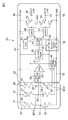
図17は従来の磁気検出装置の回路構成図である。磁気検出装置はセンサ部Sと集積回路(IC)1とから構成されている。図17に示す磁気検出装置は双極検出対応型センサである。前記センサ部Sは、正方向の外部磁界に対して抵抗値が変化するGMR素子等の第1磁気抵抗効果素子2を備えた第1ブリッジ回路BC1と、負方向の外部磁界に対して抵抗値が変化するGMR素子等の第2磁気抵抗効果素子3を備えた第2ブリッジ回路BC2とを有する。「正方向の外部磁界」とは任意の一方向の外部磁界を指すが、図20の形態では、第1磁気抵抗効果素子2の抵抗値は変動するが、第2磁気抵抗効果素子3の抵抗値は変動しない(すなわち固定抵抗として作用する)方向の外部磁界を指し、「負方向の外部磁界」とは前記正方向の外部磁界の反対方向の外部磁界であり、図20の形態では、第2磁気抵抗効果素子3の抵抗値は変動するが、第1磁気抵抗効果素子2の抵抗値は変動しない(すなわち固定抵抗として作用する)方向の外部磁界を指す。   FIG. 17 is a circuit configuration diagram of a conventional magnetic detection device. The magnetic detection device includes a sensor unit S and an integrated circuit (IC) 1. The magnetic detection device shown in FIG. 17 is a bipolar detection compatible sensor. The sensor section S includes a first bridge circuit BC1 including a first magnetoresistive element 2 such as a GMR element whose resistance value changes with respect to a positive external magnetic field, and a resistance value with respect to a negative external magnetic field. And a second bridge circuit BC2 including a second magnetoresistive element 3 such as a GMR element that changes. “External magnetic field in the positive direction” refers to an external magnetic field in one arbitrary direction. In the form of FIG. 20, the resistance value of the first magnetoresistive element 2 varies, but the resistance of the second magnetoresistive element 3 varies. The value refers to an external magnetic field in a direction that does not vary (that is, acts as a fixed resistance), and the “negative external magnetic field” is an external magnetic field in a direction opposite to the positive external magnetic field. 2 The resistance value of the magnetoresistive effect element 3 varies, but the resistance value of the first magnetoresistive effect element 2 does not vary (that is, acts as a fixed resistance).

図17に示すように、各第1磁気抵抗効果素子2は、夫々、固定抵抗素子4と直列回路を構成し、各直列回路は並列接続されて第1ブリッジ回路BC1が構成される。前記第1ブリッジ回路BC1を構成する2本の直列回路の各出力取り出し部は、第1の差動増幅器6に接続されている。また図17に示すように、各第2磁気抵抗効果素子3は、夫々、固定抵抗素子5と直列回路を構成し、各直列回路は並列接続されて第2ブリッジ回路BC2が構成される。前記第2ブリッジ回路BC2を構成する2本の直列回路の各出力取り出し部は、第2の差動増幅器7に接続されている。   As shown in FIG. 17, each first magnetoresistance effect element 2 constitutes a series circuit with the fixed resistance element 4, and each series circuit is connected in parallel to constitute a first bridge circuit BC1. Each output extraction unit of the two series circuits constituting the first bridge circuit BC1 is connected to the first differential amplifier 6. As shown in FIG. 17, each second magnetoresistive element 3 forms a series circuit with the fixed resistance element 5, and each series circuit is connected in parallel to form a second bridge circuit BC2. Each output extraction part of the two series circuits constituting the second bridge circuit BC2 is connected to the second differential amplifier 7.

前記集積回路1内には、差動増幅器6,7のほかに、シュミットトリガー型のコンパレータ12,13、ラッチ回路8,9等が設けられており、外部磁界検出信号は外部出力端子10,11から取り出される。   In the integrated circuit 1, in addition to the differential amplifiers 6 and 7, Schmitt trigger type comparators 12 and 13, latch circuits 8 and 9, and the like are provided, and external magnetic field detection signals are external output terminals 10 and 11. Taken from.

図17に示す磁気検出装置では、正方向の外部磁界が作用すると、第1ブリッジ回路BC1を構成する第1磁気抵抗効果素子2の抵抗値が変動することで、出力が前記第1の差動増幅器6で差動増幅され、それに基づき検出信号が生成されて、前記検出信号が第1外部出力端子10から出力される。一方、磁気検出装置に、負方向の外部磁界が作用すると、第2ブリッジ回路BC2を構成する第2磁気抵抗効果素子3の抵抗値が変動することで、出力が前記第2の差動増幅器7で差動増幅され、それに基づき検出信号が生成されて、前記検出信号が第2外部出力端子11から出力される。   In the magnetic detection device shown in FIG. 17, when an external magnetic field in the positive direction acts, the resistance value of the first magnetoresistance effect element 2 constituting the first bridge circuit BC1 varies, so that the output is the first differential. Differential amplification is performed by the amplifier 6, a detection signal is generated based on the differential amplification, and the detection signal is output from the first external output terminal 10. On the other hand, when a negative external magnetic field acts on the magnetic detection device, the resistance value of the second magnetoresistive element 3 constituting the second bridge circuit BC2 fluctuates, so that the output is the second differential amplifier 7. The detection signal is generated based on the differential amplification, and the detection signal is output from the second external output terminal 11.

以上のように図17に示す磁気検出装置は、正方向及び負方向のどちらの方向の外部磁界も検知可能な双極検出対応型センサとなっている。
特開2004−77374号公報 特開2004−180286号公報 特開2005−214900号公報 特開2003−14833号公報 特開2003−14834号公報 特開2003−121268号公報 特開2004−304052号公報
As described above, the magnetic detection device shown in FIG. 17 is a bipolar detection compatible sensor capable of detecting an external magnetic field in either the positive direction or the negative direction.
JP 2004-77374 A JP 2004-180286 A JP 2005-214900 A Japanese Patent Laid-Open No. 2003-14833 JP 2003-14834 A JP 2003-121268 A JP 2004-304052 A

しかしながら図17に示す従来の磁気検出装置では、センサ部Sを構成する素子数が多く必要であった。すなわち双極検出対応型センサとしたことで、ブリッジ回路BC1,BC2が2つ必要となり、素子数が合計で8個必要となった。   However, the conventional magnetic detection apparatus shown in FIG. 17 requires a large number of elements constituting the sensor unit S. In other words, since the sensor for bipolar detection is used, two bridge circuits BC1 and BC2 are required, and a total of eight elements are required.

また、ブリッジ回路BC1,BC2が2つ設けられたことで、夫々のブリッジ回路BC1,BC2に対して差動増幅器6,7、コンパレータ12,13、信号ライン等が必要となり回路構成が複雑化し、また集積回路1の小型化にも支障を来たすといった問題があった。   Further, the provision of two bridge circuits BC1 and BC2 requires differential amplifiers 6 and 7, comparators 12 and 13, signal lines and the like for each of the bridge circuits BC1 and BC2, and the circuit configuration becomes complicated. There is also a problem that the integrated circuit 1 is downsized.

そこで本発明は上記従来の課題を解決するためのものであり、特に、素子数を減らすことが出来るとともに、回路構成を簡単に出来る双極検出対応型の磁気検出装置を提供することを目的としている。   SUMMARY OF THE INVENTION Accordingly, the present invention is to solve the above-described conventional problems, and in particular, to provide a bipolar detection-compatible magnetic detection device that can reduce the number of elements and simplify the circuit configuration. .

本発明における磁気検出装置は、
第1直列回路と、第2直列回路と、第3直列回路を有し、
前記第1直列回路を構成する複数の抵抗素子には、少なくともいずれか一つに、ある一方向の外部磁界に対し電気抵抗が変化する磁気抵抗効果を利用した第1磁気抵抗効果素子が含まれ、
前記第2直列回路を構成する複数の抵抗素子には、少なくともいずれか一つに、前記一方向とは逆方向の外部磁界に対し電気抵抗が変化する第2磁気抵抗効果を利用した第2磁気抵抗効果素子が含まれ、
前記第3直列回路を構成する複数の抵抗素子は、前記第1直列回路を構成する抵抗素子、及び前記第2直列回路を構成する抵抗素子の夫々とブリッジ接続される共通の抵抗素子であり、
前記第1直列回路の第1出力取り出し部と前記第2直列回路の第2出力取り出し部は一方ずつ、第1接続切換部を介して共通の差動出力部に前記第3直列回路の第3出力取り出し部と共に接続可能とされており、
前記第1接続切換部にて、前記第1出力取り出し部と前記差動出力部が接続されたとき、前記第1直列回路と前記第3直列回路とが並列接続してなる、前記一方向の外部磁界検出用の第1ブリッジ回路が前記差動出力部に接続された状態に切り換わり、前記第1接続切換部にて、前記第2出力取り出し部と前記差動出力部が接続されたとき、前記第2直列回路と前記第3直列回路とが並列接続してなる、前記逆方向の外部磁界検出用の第2ブリッジ回路が前記差動出力部に接続された状態に切り換わることを特徴とするものである。
The magnetic detection device in the present invention is
A first series circuit, a second series circuit, and a third series circuit;
The plurality of resistive elements constituting the first series circuit include at least one of the first magnetoresistive elements using a magnetoresistive effect in which electric resistance changes with respect to an external magnetic field in one direction. ,
At least one of the plurality of resistance elements constituting the second series circuit is a second magnetic element using a second magnetoresistance effect in which an electric resistance changes with respect to an external magnetic field in a direction opposite to the one direction. Including a resistive element,
The plurality of resistance elements that constitute the third series circuit are common resistance elements that are bridge-connected to the resistance element that constitutes the first series circuit and the resistance element that constitutes the second series circuit,
One of the first output extraction unit of the first series circuit and the second output extraction unit of the second series circuit are respectively connected to the common differential output unit via the first connection switching unit. It is possible to connect with the output extraction part,
In the first connection switching unit, when the first output extraction unit and the differential output unit are connected, the first series circuit and the third series circuit are connected in parallel. When the first bridge circuit for detecting an external magnetic field is switched to the state connected to the differential output unit, and the second output extraction unit and the differential output unit are connected in the first connection switching unit. The second series circuit and the third series circuit are connected in parallel, and the second bridge circuit for detecting the external magnetic field in the reverse direction is switched to a state connected to the differential output unit. It is what.

本発明では、上記構成により双極検出対応型の磁気検出装置において、従来よりも素子数を減らすことが出来るとともに、回路構成を簡単に出来る。すなわち本発明では、第3直列回路を第1ブリッジ回路及び第2ブリッジ回路の共通配線としたことで、従来に比べて、2つのブリッジ形成に必要な素子数を減らすことができる。しかも、本発明では、第1接続切換部を設けて、第1出力取り出し部及び第2出力取り出し部の差動出力部への接続を切り換えることで、第1ブリッジ回路が差動出力部に接続された状態と、第2ブリッジ回路が差動出力部に接続された状態との2状態を簡単な回路構成で得ることが出来る。   In the present invention, in the magnetic detection device compatible with bipolar detection, the number of elements can be reduced as compared with the conventional one and the circuit configuration can be simplified. That is, in the present invention, the third series circuit is a common wiring for the first bridge circuit and the second bridge circuit, so that the number of elements required for forming two bridges can be reduced as compared with the conventional case. Moreover, in the present invention, the first bridge circuit is connected to the differential output unit by providing the first connection switching unit and switching the connection of the first output extraction unit and the second output extraction unit to the differential output unit. Two states, that is, a state where the second bridge circuit is connected to the differential output unit, can be obtained with a simple circuit configuration.

また本発明では、前記第1直列回路は、第1抵抗素子と、第2抵抗素子とが前記第1の出力取り出し部を介して直列接続され、前記第1抵抗素子が前記第1磁気抵抗効果素子で形成され、
前記第2直列回路は、第3抵抗素子と、第4抵抗素子とが前記第2の出力取り出し部を介して、直列接続されてなり、前記第3抵抗素子が前記第2磁気抵抗効果素子で形成され、
前記第3直列回路は、第5抵抗素子と第6抵抗素子とが前記第3の出力取り出し部を介して、直列接続され、
前記第1抵抗素子と、前記第6抵抗素子とが並列接続されるとともに、前記第2抵抗素子と前記第5抵抗素子とが並列接続されて、前記第1ブリッジ回路が構成され、
前記第3抵抗素子と、前記第5抵抗素子とが並列接続されるとともに、前記第4抵抗素子と前記第6抵抗素子とが並列接続されて、前記第2ブリッジ回路が構成されていることが好ましい。
In the present invention, the first series circuit includes a first resistance element and a second resistance element connected in series via the first output extraction section, and the first resistance element is the first magnetoresistive effect. Formed of elements,
The second series circuit includes a third resistance element and a fourth resistance element connected in series via the second output extraction unit, and the third resistance element is the second magnetoresistance effect element. Formed,
In the third series circuit, a fifth resistance element and a sixth resistance element are connected in series via the third output extraction unit,
The first resistance element and the sixth resistance element are connected in parallel, and the second resistance element and the fifth resistance element are connected in parallel to form the first bridge circuit,
The third resistor element and the fifth resistor element are connected in parallel, and the fourth resistor element and the sixth resistor element are connected in parallel to form the second bridge circuit. preferable.

また本発明では、第1外部出力端子と、第2外部出力端子と、前記差動出力部と前記第1外部出力端子間の接続、及び前記差動出力部と前記第2外部出力端子間の接続を切り換える第2接続切換部と、を備え、
前記第1接続切換部により前記第1出力取り出し部と前記差動出力部間が接続されたとき、前記第2接続切換部により前記差動出力部と前記第1外部出力端子間が接続され、前記第1接続切換部により前記第2出力取り出し部と前記差動出力部間が接続されたとき、前記第2接続切換部により前記差動出力部と前記第2外部出力端子間が接続されることが好ましい。
In the present invention, the first external output terminal, the second external output terminal, the connection between the differential output unit and the first external output terminal, and between the differential output unit and the second external output terminal A second connection switching unit for switching the connection,
When the first output switching unit and the differential output unit are connected by the first connection switching unit, the differential output unit and the first external output terminal are connected by the second connection switching unit, When the second output extraction unit and the differential output unit are connected by the first connection switching unit, the differential output unit and the second external output terminal are connected by the second connection switching unit. It is preferable.

本発明では、簡単な回路構成で、外部磁界方向の検知も可能な2出力の双極検出対応型センサにできる。   In the present invention, a two-output bipolar detection compatible sensor capable of detecting the direction of the external magnetic field with a simple circuit configuration can be provided.

また本発明では、入力端子及びアース端子の少なくともどちらか一方の端子と前記第1直列回路間の接続、及び前記一方の端子と前記第2直列回路間の接続とを切り換える第3接続切換部を備え、
前記第1接続切換部により前記第1出力取り出し部と前記差動出力部間が接続されたとき、前記第3接続切換部により前記第1直列回路と前記一方の端子間が接続され、前記第1接続切換部により前記第2出力取り出し部と前記差動出力部間が接続されたとき、前記第3接続切換部により前記第2直列回路と前記一方の端子間が接続されることが好ましい。これにより、第1直列回路及び第2直列回路のうち差動出力部に接続されていない側の直列回路に電流が流れず、消費電流の低減を図ることが出来、また検出感度を向上させることが出来る。
In the present invention, a third connection switching unit that switches between a connection between at least one of the input terminal and the ground terminal and the first series circuit, and a connection between the one terminal and the second series circuit. Prepared,
When the first output switching unit and the differential output unit are connected by the first connection switching unit, the first series circuit and the one terminal are connected by the third connection switching unit. When the second output extraction unit and the differential output unit are connected by the one connection switching unit, it is preferable that the second series circuit and the one terminal are connected by the third connection switching unit. As a result, no current flows through the series circuit on the side of the first series circuit and the second series circuit that is not connected to the differential output unit, so that current consumption can be reduced and detection sensitivity can be improved. I can do it.

本発明では、双極検出対応型の磁気検出装置において、従来よりも素子数を減らすことが出来るとともに、回路構成を簡単に出来る。さらに消費電流を低減できる。   In the present invention, the number of elements can be reduced and the circuit configuration can be simplified in the magnetic detection device for bipolar detection. Furthermore, current consumption can be reduced.

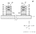
図1,図2は本実施形態の磁気検出装置20の回路構成図、図3は第1磁気抵抗効果素子のヒステリシス特性を説明するためのグラフ(R−H曲線)、図4は第2磁気抵抗効果素子のヒステリシス特性を説明するためのグラフ(R−H曲線)、図5は本実施形態の磁気検出装置20のセンサ部の抵抗素子形状を示す磁気検出装置20の部分拡大斜視図、図6は図5に示すA−A線から厚さ方向に前記磁気検出装置を切断し矢印方向から見た前記磁気検出装置の部分断面図、図7は、第1磁気抵抗効果素子及び第2磁気抵抗効果素子の層構造を示す部分断面図、図8は、主に固定抵抗素子の層構造を説明するための部分断面図、図9〜図16は、本実施形態の磁気検出装置の用途を説明するための一例であり、前記磁気検出装置を内臓した折畳み式携帯電話の部分模式図や部分平面図、である。   1 and 2 are circuit configuration diagrams of the magnetic detection device 20 of the present embodiment, FIG. 3 is a graph (RH curve) for explaining the hysteresis characteristics of the first magnetoresistance effect element, and FIG. 4 is a second magnetic field. FIG. 5 is a partially enlarged perspective view of the magnetic detection device 20 showing the shape of the resistance element of the sensor unit of the magnetic detection device 20 according to the present embodiment. 6 is a partial cross-sectional view of the magnetic detection device when the magnetic detection device is cut in the thickness direction from the line AA shown in FIG. 5 and viewed from the arrow direction, and FIG. 7 is the first magnetoresistive element and the second magnetic resistance. FIG. 8 is a partial cross-sectional view mainly illustrating the layer structure of the fixed resistance element, and FIGS. 9 to 16 illustrate the use of the magnetic detection device of the present embodiment. It is an example for demonstrating and the folding which incorporated the said magnetic detection apparatus Partial schematic diagram and partial plan view of the Formula mobile phone is.

図1に示す本実施形態の磁気検出装置20は、センサ部21と集積回路(IC)22とを有して構成される。   A magnetic detection device 20 according to this embodiment shown in FIG. 1 includes a sensor unit 21 and an integrated circuit (IC) 22.

前記センサ部21には、第1抵抗素子(第1磁気抵抗効果素子)23と第2抵抗素子(本実施形態では固定抵抗素子)24とが第1出力取り出し部(接続部)25を介して直列接続された第1直列回路26、第3抵抗素子(第2磁気抵抗効果素子)27と第4抵抗素子(本実施形態では固定抵抗素子)28とが第2出力取り出し部(接続部)29を介して直列接続された第2直列回路30、及び、第5抵抗素子(本実施形態では固定抵抗素子)31と第6抵抗素子(本実施形態では固定抵抗素子)32が第3出力取り出し部33を介して直列接続された第3直列回路34が設けられる。   The sensor unit 21 includes a first resistance element (first magnetoresistance effect element) 23 and a second resistance element (fixed resistance element in the present embodiment) 24 through a first output extraction unit (connection unit) 25. A first series circuit 26, a third resistance element (second magnetoresistive effect element) 27, and a fourth resistance element (fixed resistance element in the present embodiment) 28 connected in series are a second output extraction section (connection section) 29. A second series circuit 30, and a fifth resistor element (fixed resistor element in the present embodiment) 31 and a sixth resistor element (fixed resistor element in the present embodiment) 32 connected in series via the third output circuit. A third series circuit 34 connected in series via 33 is provided.

なお上記のように「抵抗素子」の表記は、第1〜第6までの通し番号とした。なお以下では、各抵抗素子を、主に「磁気抵抗効果素子」及び「固定抵抗素子」として表記し、「磁気抵抗効果素子」及び「固定抵抗素子」と区別する必要のない説明箇所については「抵抗素子」の表記を使用することとした。   As described above, the notation of “resistance element” is a serial number from the first to the sixth. In the following, each resistance element will be mainly described as “magnetoresistance effect element” and “fixed resistance element”, and for explanation parts that do not need to be distinguished from “magnetoresistance effect element” and “fixed resistance element”, “ The notation “resistance element” was used.

前記第3直列回路34は、共通回路として前記第1直列回路26及び前記第2直列回路30と夫々ブリッジ回路を構成している。以下では前記第1直列回路26と前記第3直列回路34とが並列接続されてなるブリッジ回路を第1ブリッジ回路BC3と、前記第2直列回路30と前記第3直列回路34とが並列接続されてなるブリッジ回路を第2ブリッジ回路BC4と称する。   The third series circuit 34 forms a bridge circuit with the first series circuit 26 and the second series circuit 30 as a common circuit. In the following, a bridge circuit in which the first series circuit 26 and the third series circuit 34 are connected in parallel is a first bridge circuit BC3, and the second series circuit 30 and the third series circuit 34 are connected in parallel. This bridge circuit is referred to as a second bridge circuit BC4.

図1に示すように、前記第1ブリッジ回路BC3では、第1抵抗素子23と、前第6抵抗素子32とが並列接続されるとともに、前記第2抵抗素子24と前記第5抵抗素子31とが並列接続されている。また前記第2ブリッジ回路BC4では、前記第3抵抗素子27と、前記第5抵抗素子31とが並列接続されるとともに、前記第4抵抗素子28と前記第6抵抗素子32とが並列接続されている。   As shown in FIG. 1, in the first bridge circuit BC3, the first resistance element 23 and the front sixth resistance element 32 are connected in parallel, and the second resistance element 24 and the fifth resistance element 31 are connected to each other. Are connected in parallel. In the second bridge circuit BC4, the third resistance element 27 and the fifth resistance element 31 are connected in parallel, and the fourth resistance element 28 and the sixth resistance element 32 are connected in parallel. Yes.

図1に示すように前記集積回路22には入力端子(電源)39、アース端子42及び2つの外部出力端子40,41が設けられている。前記入力端子39、アース端子42及び外部出力端子40,41は夫々図示しない機器側の端子部とワイヤボンディングやダイボンディング等で電気的に接続されている。   As shown in FIG. 1, the integrated circuit 22 is provided with an input terminal (power source) 39, a ground terminal 42, and two external output terminals 40 and 41. The input terminal 39, the ground terminal 42, and the external output terminals 40 and 41 are electrically connected to terminal portions on the device side (not shown) by wire bonding, die bonding or the like.

前記入力端子39に接続された信号ライン50及び前記アース端子42に接続された信号ライン51は、前記第1直列回路26,第2直列回路30及び第3直列回路34の両側端部に設けられた電極の夫々に接続されている。   A signal line 50 connected to the input terminal 39 and a signal line 51 connected to the ground terminal 42 are provided at both ends of the first series circuit 26, the second series circuit 30, and the third series circuit 34. Connected to each of the electrodes.

図1に示すように集積回路22内には、1つの差動増幅器(差動出力部)35が設けられ、前記差動増幅器35の+入力部、−入力部のどちらかに、前記第3直列回路34の第3出力取り出し部33が接続されている。なお、前記第3出力取り出し部33と前記差動増幅器35の接続は、次に説明する、前記第1直列回路26の第1出力取り出し部25及び第2直列回路30の第2出力取り出し部29と差動増幅器35間の接続状態と異なって固定されている(非接続状態にはならない)。   As shown in FIG. 1, one differential amplifier (differential output unit) 35 is provided in the integrated circuit 22, and either the + input unit or the −input unit of the differential amplifier 35 is connected to the third input unit. A third output extraction unit 33 of the series circuit 34 is connected. The connection between the third output extraction unit 33 and the differential amplifier 35 is described below. The first output extraction unit 25 of the first series circuit 26 and the second output extraction unit 29 of the second series circuit 30 will be described below. Unlike the connection state between the differential amplifier 35 and the differential amplifier 35, they are fixed (not connected).

前記第1直列回路26の第1出力取り出し部25及び第2直列回路30の第2出力取り出し部29は夫々第1スイッチ回路(第1接続切換部)36の入力部に接続され、前記第1スイッチ回路36の出力部は前記差動増幅器35の−入力部、+入力部のどちらか(前記第3出力取り出し部33が接続されていない側の入力部)に接続されている。   The first output extraction unit 25 of the first series circuit 26 and the second output extraction unit 29 of the second series circuit 30 are respectively connected to the input unit of a first switch circuit (first connection switching unit) 36, and the first The output section of the switch circuit 36 is connected to either the − input section or the + input section of the differential amplifier 35 (the input section on the side where the third output extraction section 33 is not connected).

図1に示すように、前記差動増幅器35の出力部はシュミットトリガー型のコンパレータ38に接続され、さらに前記コンパレータ38の出力部は第2のスイッチ回路(第2接続切換部)43の入力部に接続され、さらに前記第2スイッチ回路43の出力部側は2つのラッチ回路46,47及びFET回路54、55を経て第1外部出力端子40及び第2外部出力端子41に夫々接続される。   As shown in FIG. 1, the output section of the differential amplifier 35 is connected to a Schmitt trigger type comparator 38, and the output section of the comparator 38 is an input section of a second switch circuit (second connection switching section) 43. Furthermore, the output side of the second switch circuit 43 is connected to the first external output terminal 40 and the second external output terminal 41 via the two latch circuits 46 and 47 and the FET circuits 54 and 55, respectively.

さらに図1に示すように、前記集積回路22内には第3のスイッチ回路48が設けられている。前記第3のスイッチ回路48の出力部は、前記アース端子42に接続された信号ライン51に接続され、前記第3のスイッチ回路48の入力部には、第1直列回路26及び第2直列回路30の一端部が接続されている。   Further, as shown in FIG. 1, a third switch circuit 48 is provided in the integrated circuit 22. The output part of the third switch circuit 48 is connected to a signal line 51 connected to the ground terminal 42, and the first series circuit 26 and the second series circuit are connected to the input part of the third switch circuit 48. One end of 30 is connected.

さらに図1に示すように、前記集積回路22内には、インターバルスイッチ回路52及びクロック回路53が設けられている。前記インターバルスイッチ回路52のスイッチがオフされると集積回路22内への通電が停止するようになっている。前記インターバルスイッチ回路52のスイッチのオン・オフは、前記クロック回路53からのクロック信号に連動しており、前記インターバルスイッチ回路52は通電状態を間欠的に行う節電機能を有している。   Further, as shown in FIG. 1, an interval switch circuit 52 and a clock circuit 53 are provided in the integrated circuit 22. When the switch of the interval switch circuit 52 is turned off, the power supply to the integrated circuit 22 is stopped. The on / off of the switch of the interval switch circuit 52 is interlocked with the clock signal from the clock circuit 53, and the interval switch circuit 52 has a power saving function for intermittently energizing.

前記クロック回路53からのクロック信号は、第1スイッチ回路36、第2スイッチ回路43、及び第3スイッチ回路48にも出力される。前記第1スイッチ回路36、第2スイッチ回路43、及び第3スイッチ回路48では前記クロック信号を受けると、そのクロック信号を分割し、非常に短い周期でスイッチ動作を行うように制御されている。例えば1パルスのクロック信号が数十msecであるとき、数十μmsec毎にスイッチ動作を行う。   The clock signal from the clock circuit 53 is also output to the first switch circuit 36, the second switch circuit 43, and the third switch circuit 48. When receiving the clock signal, the first switch circuit 36, the second switch circuit 43, and the third switch circuit 48 are controlled so as to divide the clock signal and perform the switch operation with a very short cycle. For example, when one pulse of the clock signal is several tens of milliseconds, the switching operation is performed every several tens of micrometers.

前記第1磁気抵抗効果素子23は正方向の外部磁界(+H)の強度変化に基づいて磁気抵抗効果を発揮する磁気抵抗効果素子であり、一方、前記第2磁気抵抗効果素子27は、前記正方向と反対方向である負方向の外部磁界(−H)の磁界強度変化に基づいて磁気抵抗効果を発揮する磁気抵抗効果素子である。   The first magnetoresistive element 23 is a magnetoresistive element that exhibits a magnetoresistive effect based on a change in the strength of an external magnetic field (+ H) in the positive direction, while the second magnetoresistive element 27 is the positive magnetoresistive element 27. This is a magnetoresistive element that exhibits a magnetoresistive effect based on a change in magnetic field strength of an external magnetic field (-H) in the negative direction that is opposite to the direction.

ここで、正方向の外部磁界(+H)はある一方向を示し、本実施形態では、図示X1方向に向く方向である。この方向の外部磁界が作用すると、図3,図4で説明するように、第1磁気抵抗効果素子23の抵抗値は変動するが、第2磁気抵抗効果素子27の抵抗値は変動しない(すなわち固定抵抗として作用する)。   Here, the external magnetic field (+ H) in the positive direction indicates a certain direction, and in the present embodiment, the direction is in the X1 direction in the drawing. When an external magnetic field in this direction acts, the resistance value of the first magnetoresistance effect element 23 varies as shown in FIGS. 3 and 4, but the resistance value of the second magnetoresistance effect element 27 does not vary (that is, Acts as a fixed resistance).

一方、負方向の外部磁界(−H)は、前記正方向とは逆方向の外部磁界であり、図示X2方向に向く方向である。この方向の外部磁界が作用すると、図3,図4で説明するように、第2磁気抵抗効果素子27の抵抗値は変動するが、第1磁気抵抗効果素子23の抵抗値は変動しない(すなわち固定抵抗として作用する)。   On the other hand, the negative external magnetic field (-H) is an external magnetic field in the direction opposite to the positive direction, and is the direction facing the X2 direction in the figure. When an external magnetic field in this direction acts, the resistance value of the second magnetoresistive effect element 27 changes as shown in FIGS. 3 and 4, but the resistance value of the first magnetoresistive effect element 23 does not change (that is, Acts as a fixed resistance).

前記第1磁気抵抗効果素子23及び第2磁気抵抗効果素子27の層構造及びヒステリシス特性について以下で詳しく説明する。   The layer structure and hysteresis characteristics of the first magnetoresistive element 23 and the second magnetoresistive element 27 will be described in detail below.

図7に示すように、前記第1の磁気抵抗効果素子23及び第2の磁気抵抗効果素子27は共に、下から下地層60,シード層61、反強磁性層62、固定磁性層63、非磁性中間層64、フリー磁性層65,67(第2磁気抵抗効果素子27のフリー磁性層を符号37とした)、及び保護層66の順で積層されている。前記下地層60は、例えば、Ta,Hf,Nb,Zr,Ti,Mo,Wのうち1種または2種以上の元素などの非磁性材料で形成される。前記シード層61は、NiFeCrあるいはCr等で形成される。前記反強磁性層62は、元素α(ただしαは、Pt,Pd,Ir,Rh,Ru,Osのうち1種または2種以上の元素である)とMnとを含有する反強磁性材料、又は、元素αと元素α′(ただし元素α′は、Ne,Ar,Kr,Xe,Be,B,C,N,Mg,Al,Si,P,Ti,V,Cr,Fe,Co,Ni,Cu,Zn,Ga,Ge,Zr,Nb,Mo,Ag,Cd,Sn,Hf,Ta,W,Re,Au,Pb、及び希土類元素のうち1種または2種以上の元素である)とMnとを含有する反強磁性材料で形成される。例えば前記反強磁性層62は、IrMnやPtMnで形成される。前記固定磁性層63及びフリー磁性層65,67はCoFe合金、NiFe合金、CoFeNi合金等の磁性材料で形成される。また前記非磁性中間層64はCu等で形成される。また前記保護層66はTa等で形成される。前記固定磁性層63やフリー磁性層65,67は積層フェリ構造(磁性層/非磁性層/磁性層の積層構造であり、非磁性層を挟んだ2つの磁性層の磁化方向が反平行である構造)であってもよい。また前記固定磁性層63やフリー磁性層65,67は材質の異なる複数の磁性層の積層構造であってもよい。   As shown in FIG. 7, the first magnetoresistive effect element 23 and the second magnetoresistive effect element 27 are both the base layer 60, the seed layer 61, the antiferromagnetic layer 62, the fixed magnetic layer 63, the non-magnetic layer 63 from the bottom. The magnetic intermediate layer 64, the free magnetic layers 65 and 67 (the free magnetic layer of the second magnetoresistive effect element 27 is denoted by reference numeral 37), and the protective layer 66 are laminated in this order. The underlayer 60 is made of, for example, a nonmagnetic material such as one or more elements selected from Ta, Hf, Nb, Zr, Ti, Mo, and W. The seed layer 61 is made of NiFeCr or Cr. The antiferromagnetic layer 62 includes an anti-ferromagnetic material containing an element α (where α is one or more of Pt, Pd, Ir, Rh, Ru, and Os) and Mn. Or, element α and element α ′ (where element α ′ is Ne, Ar, Kr, Xe, Be, B, C, N, Mg, Al, Si, P, Ti, V, Cr, Fe, Co, Ni) , Cu, Zn, Ga, Ge, Zr, Nb, Mo, Ag, Cd, Sn, Hf, Ta, W, Re, Au, Pb, and rare earth elements are one or more elements) and It is formed of an antiferromagnetic material containing Mn. For example, the antiferromagnetic layer 62 is made of IrMn or PtMn. The fixed magnetic layer 63 and the free magnetic layers 65 and 67 are formed of a magnetic material such as a CoFe alloy, a NiFe alloy, or a CoFeNi alloy. The nonmagnetic intermediate layer 64 is made of Cu or the like. The protective layer 66 is made of Ta or the like. The pinned magnetic layer 63 and the free magnetic layers 65 and 67 have a laminated ferrimagnetic structure (magnetic layer / nonmagnetic layer / magnetic layer laminated structure, and the magnetization directions of two magnetic layers sandwiching the nonmagnetic layer are antiparallel. Structure). The pinned magnetic layer 63 and the free magnetic layers 65 and 67 may have a laminated structure of a plurality of magnetic layers made of different materials.

前記第1の磁気抵抗効果素子23及び第2の磁気抵抗効果素子27では、前記反強磁性層62と前記固定磁性層63とが接して形成されているため磁場中熱処理を施すことにより前記反強磁性層62と前記固定磁性層63との界面に交換結合磁界(Hex)が生じ、前記固定磁性層63の磁化方向は一方向に固定される。図5及び図7では、前記固定磁性層63の磁化方向63aを矢印方向で示している。第1の磁気抵抗効果素子23及び第2の磁気抵抗効果素子27において前記固定磁性層63の磁化方向63aは共に図示X1方向(正方向)である。   In the first magnetoresistive element 23 and the second magnetoresistive element 27, the antiferromagnetic layer 62 and the fixed magnetic layer 63 are formed in contact with each other. An exchange coupling magnetic field (Hex) is generated at the interface between the ferromagnetic layer 62 and the fixed magnetic layer 63, and the magnetization direction of the fixed magnetic layer 63 is fixed in one direction. 5 and 7, the magnetization direction 63a of the pinned magnetic layer 63 is indicated by the arrow direction. In the first magnetoresistive effect element 23 and the second magnetoresistive effect element 27, the magnetization direction 63a of the fixed magnetic layer 63 is the X1 direction (positive direction) shown in the drawing.

一方、前記フリー磁性層65,67の磁化方向は、第1の磁気抵抗効果素子23と第2の磁気抵抗効果素子27とで異なっている。図7に示すように前記第1の磁気抵抗効果素子23では前記フリー磁性層65の磁化方向65aが図示X2方向(負方向)であり、固定磁性層63の磁化方向63aと同じ方向であるが、前記第2の磁気抵抗効果素子27では前記フリー磁性層67の磁化方向67aが図示X1方向(正方向)であり、前記固定磁性層63の磁化方向63aと反平行である。   On the other hand, the magnetization directions of the free magnetic layers 65 and 67 differ between the first magnetoresistive element 23 and the second magnetoresistive element 27. As shown in FIG. 7, in the first magnetoresistive element 23, the magnetization direction 65a of the free magnetic layer 65 is the X2 direction (negative direction) shown in the figure, and is the same direction as the magnetization direction 63a of the pinned magnetic layer 63. In the second magnetoresistive element 27, the magnetization direction 67a of the free magnetic layer 67 is the X1 direction (positive direction) in the drawing, and is antiparallel to the magnetization direction 63a of the pinned magnetic layer 63.

正方向の外部磁界(+H)が作用すると、第2の磁気抵抗効果素子27のフリー磁性層67の磁化67aは変動しないが、第1の磁気抵抗効果素子23のフリー磁性層65の磁化65aは変動して前記第1の磁気抵抗効果素子23の抵抗値は変化する。図3は第1の磁気抵抗効果素子23のヒステリシス特性を示すR−H曲線である。なお図のグラフでは縦軸が抵抗値Rであるが、抵抗変化率(%)であってもよい。図3に示すように、外部磁界が無磁場状態(ゼロ)から徐々に正方向に増加していくと、フリー磁性層65の磁化65aと固定磁性層63の磁化63aとの平行状態が崩れて反平行状態に近づくため前記第1の磁気抵抗効果素子23の抵抗値Rは、曲線HR1上を辿って徐々に大きくなり、正方向の外部磁界(+H)を徐々にゼロに向けて小さくしていくと、前記第1の磁気抵抗効果素子23の抵抗値Rは、曲線HR2上を辿って徐々に小さくなる。   When a positive external magnetic field (+ H) acts, the magnetization 67a of the free magnetic layer 67 of the second magnetoresistance effect element 27 does not change, but the magnetization 65a of the free magnetic layer 65 of the first magnetoresistance effect element 23 changes. The resistance value of the first magnetoresistive effect element 23 changes as it fluctuates. FIG. 3 is an RH curve showing the hysteresis characteristic of the first magnetoresistive element 23. In the graph of the figure, the vertical axis is the resistance value R, but it may be the resistance change rate (%). As shown in FIG. 3, when the external magnetic field gradually increases in the positive direction from the zero magnetic field state (zero), the parallel state between the magnetization 65a of the free magnetic layer 65 and the magnetization 63a of the pinned magnetic layer 63 collapses. In order to approach the antiparallel state, the resistance value R of the first magnetoresistive element 23 gradually increases along the curve HR1, and the positive external magnetic field (+ H) is gradually decreased toward zero. As a result, the resistance value R of the first magnetoresistance effect element 23 gradually decreases along the curve HR2.

このように、第1の磁気抵抗効果素子23には正方向の外部磁界(+H)の磁界強度変化に対して、曲線HR1と曲線HR2で囲まれたヒステリシスループHRが形成される。前記第1の磁気抵抗効果素子23の最大抵抗値と最低抵抗値の中間値であって、前記ヒステリシスループHRの広がり幅の中心値がヒステリシスループHRの「中点」である。そして前記ヒステリシスループHRの中点から外部磁界H=0(Oe)のラインまでの磁界の強さで第1の層間結合磁界Hin1の大きさが決定される。図3に示すように第1の磁気抵抗効果素子23では、前記第1の層間結合磁界Hin1が正の磁界方向へシフトしている。   As described above, the first magnetoresistance effect element 23 is formed with the hysteresis loop HR surrounded by the curves HR1 and HR2 with respect to the magnetic field strength change of the external magnetic field (+ H) in the positive direction. The intermediate value of the maximum resistance value and the minimum resistance value of the first magnetoresistance effect element 23, and the center value of the spread width of the hysteresis loop HR is the “midpoint” of the hysteresis loop HR. The magnitude of the first interlayer coupling magnetic field Hin1 is determined by the strength of the magnetic field from the midpoint of the hysteresis loop HR to the line of the external magnetic field H = 0 (Oe). As shown in FIG. 3, in the first magnetoresistive element 23, the first interlayer coupling magnetic field Hin1 is shifted in the positive magnetic field direction.

一方、負方向の外部磁界(−H)が及ぼされると、前記第1の磁気抵抗効果素子23のフリー磁性層65の磁化65aは変動しないが、第2の磁気抵抗効果素子27のフリー磁性層67の磁化67aは変動して前記第2の磁気抵抗効果素子27の抵抗値が変動する。   On the other hand, when a negative external magnetic field (−H) is applied, the magnetization 65 a of the free magnetic layer 65 of the first magnetoresistive effect element 23 does not change, but the free magnetic layer of the second magnetoresistive effect element 27. The magnetization 67a of 67 changes and the resistance value of the second magnetoresistive element 27 changes.

図4は第2の磁気抵抗効果素子27のヒステリシス特性を示すR−H曲線である。図4に示すように、外部磁界が無磁場状態(ゼロ)から徐々に負方向に増加していくと、フリー磁性層67の磁化67aと固定磁性層63の磁化63aとの反平行状態が崩れて平行状態に近づくため、前記第2の磁気抵抗効果素子27の抵抗値Rは、曲線HR3上を辿って徐々に小さくなり、一方、負方向の外部磁界(−H)を徐々にゼロに向けて変化させると、前記第2の磁気抵抗効果素子27の抵抗値Rは、曲線HR4上を辿って徐々に大きくなる。   FIG. 4 is an RH curve showing the hysteresis characteristic of the second magnetoresistive element 27. As shown in FIG. 4, when the external magnetic field gradually increases in the negative direction from the non-magnetic state (zero), the antiparallel state between the magnetization 67a of the free magnetic layer 67 and the magnetization 63a of the pinned magnetic layer 63 collapses. Accordingly, the resistance value R of the second magnetoresistive element 27 gradually decreases along the curve HR3, while the negative external magnetic field (-H) is gradually directed to zero. The resistance value R of the second magnetoresistance effect element 27 gradually increases along the curve HR4.

このように、第2の磁気抵抗効果素子27には負方向の外部磁界(−H)の磁界強度変化に対して、曲線HR3と曲線HR4で囲まれたヒステリシスループHRが形成される。前記第2の磁気抵抗効果素子27の最大抵抗値と最低抵抗値の中間値であって、前記ヒステリシスループHRの広がり幅の中心値がヒステリシスループHRの「中点」である。そして前記ヒステリシスループHRの中点から外部磁界H=0(Oe)のラインまでの磁界の強さで第2の層間結合磁界Hin2の大きさが決定される。図4に示すように第2の磁気抵抗効果素子27では、前記第2の層間結合磁界Hin2が負の磁界方向へシフトしている。   As described above, the second magnetoresistance effect element 27 is formed with the hysteresis loop HR surrounded by the curves HR3 and HR4 with respect to the change in the magnetic field strength of the external magnetic field (−H) in the negative direction. The intermediate value of the maximum resistance value and the minimum resistance value of the second magnetoresistive element 27, and the center value of the spread width of the hysteresis loop HR is the “midpoint” of the hysteresis loop HR. The magnitude of the second interlayer coupling magnetic field Hin2 is determined by the strength of the magnetic field from the midpoint of the hysteresis loop HR to the line of the external magnetic field H = 0 (Oe). As shown in FIG. 4, in the second magnetoresistive element 27, the second interlayer coupling magnetic field Hin2 is shifted in the negative magnetic field direction.

このように本実施形態では、前記第1の磁気抵抗効果素子23の第1の層間結合磁界Hin1は、正の磁界方向にシフトし、一方、前記第2の磁気抵抗効果素子27の第2の層間結合磁界Hin2は、負の磁界方向にシフトしている。   Thus, in the present embodiment, the first interlayer coupling magnetic field Hin1 of the first magnetoresistive element 23 is shifted in the positive magnetic field direction, while the second magnetoresistive element 27 of the second magnetoresistive element 27 is The interlayer coupling magnetic field Hin2 is shifted in the negative magnetic field direction.

図3、図4で説明した互いに逆符号の層間結合磁界Hin1,Hin2を得るには、例えば、前記非磁性中間層64の表面に対するプラズマトリートメント(PT)の際の、ガス流量(ガス圧)や電力値を適切に調整すればよい。ガス流量(ガス圧)の大きさ、及び電力値の大きさに応じて、層間結合磁界Hinが変化することがわかっている。前記ガス流量(ガス圧)や電力値を大きくするほど層間結合磁界Hinを正値から負値へ変化させることができる。また、前記層間結合磁界Hinの大きさは前記非磁性中間層64の膜厚でも変化する。あるいは、前記層間結合磁界Hinの大きさは、下から、反強磁性層/固定磁性層/非磁性中間層/フリー磁性層の順に積層されている場合に、前記反強磁性層の膜厚を変えることでも調整できる。   In order to obtain the interlayer coupling magnetic fields Hin1 and Hin2 having the opposite signs described in FIG. 3 and FIG. 4, for example, the gas flow rate (gas pressure) and the like during plasma treatment (PT) on the surface of the nonmagnetic intermediate layer 64 What is necessary is just to adjust an electric power value appropriately. It is known that the interlayer coupling magnetic field Hin changes depending on the magnitude of the gas flow rate (gas pressure) and the magnitude of the power value. The interlayer coupling magnetic field Hin can be changed from a positive value to a negative value as the gas flow rate (gas pressure) or power value is increased. The magnitude of the interlayer coupling magnetic field Hin also changes with the film thickness of the nonmagnetic intermediate layer 64. Alternatively, when the magnitude of the interlayer coupling magnetic field Hin is laminated from the bottom in the order of antiferromagnetic layer / pinned magnetic layer / nonmagnetic intermediate layer / free magnetic layer, the film thickness of the antiferromagnetic layer is set as follows. It can be adjusted by changing.

第1の磁気抵抗効果素子23では第1の前記層間結合磁界Hin1が正値であり、かかる場合には前記固定磁性層63と前記フリー磁性層65間には互いの磁化を平行にしようとする相互作用が働く。また、第2の磁気抵抗効果素子27では第2の前記層間結合磁界Hin2が負値であり、かかる場合には前記固定磁性層63と前記フリー磁性層67間には互いの磁化を反平行にしようとする相互作用が働く。そして、各磁気抵抗効果素子23,27の反強磁性層62と固定磁性層63との間に同一方向の交換結合磁界(Hex)を磁場中熱処理にて生じさせることで、各磁気抵抗効果素子23,27の固定磁性層63の磁化63aを同一方向に固定でき、また固定磁性層63とフリー磁性層65,67との間には上記した相互作用が働いて、図7の磁化状態となる。   In the first magnetoresistive element 23, the first interlayer coupling magnetic field Hin1 is a positive value. In such a case, the magnetization between the fixed magnetic layer 63 and the free magnetic layer 65 is made parallel to each other. Interaction works. In the second magnetoresistive element 27, the second interlayer coupling magnetic field Hin2 has a negative value. In such a case, the magnetizations of the fixed magnetic layer 63 and the free magnetic layer 67 are antiparallel to each other. The intended interaction works. Then, by generating an exchange coupling magnetic field (Hex) in the same direction between the antiferromagnetic layer 62 and the pinned magnetic layer 63 of each magnetoresistive effect element 23, 27 by heat treatment in the magnetic field, each magnetoresistive effect element. The magnetization 63a of the pinned magnetic layer 63 of 27 and 27 can be pinned in the same direction, and the above-described interaction acts between the pinned magnetic layer 63 and the free magnetic layers 65 and 67, resulting in the magnetized state of FIG. .

上記した第1磁気抵抗効果素子23及び第2磁気抵抗効果素子27は巨大磁気抵抗効果(GMR効果)を利用したものであったが、GMR素子以外に、異方性磁気抵抗効果(AMR)を利用したAMR素子やトンネル磁気抵抗効果(TMR)を利用したTMR素子であってもよい。   The first magnetoresistive effect element 23 and the second magnetoresistive effect element 27 described above utilize the giant magnetoresistive effect (GMR effect). However, in addition to the GMR element, the anisotropic magnetoresistive effect (AMR) is used. It may be a TMR element using an AMR element or a tunnel magnetoresistive effect (TMR).

一方、第1の磁気抵抗効果素子23に直列接続される固定抵抗素子24は、前記第1の磁気抵抗効果素子23と積層順が異なるだけで、前記第1の磁気抵抗効果素子23と同じ材料層で形成される。すなわち図8に示すように、前記固定抵抗素子24は下から下地層60、シード層61、反強磁性層62、第1磁性層63、第2磁性層65、非磁性中間層64、及び保護層66の順に積層される。前記第1磁性層63が、第1の磁気抵抗効果素子23を構成する固定磁性層63に該当し、前記第2磁性層65が前記第1の磁気抵抗効果素子23を構成するフリー磁性層65に該当している。図8に示すように、前記固定抵抗素子23では、前記反強磁性層62上に第1磁性層63及び第2磁性層65が連続して積層されて第1磁性層63及び第2磁性層65の磁化は共に、反強磁性層62との間で生じる交換結合磁界(Hex)により固定されており、前記第2磁性層65は前記第1の磁気抵抗効果素子23のフリー磁性層65のように外部磁界に対して磁化変動しない。   On the other hand, the fixed resistive element 24 connected in series to the first magnetoresistive effect element 23 is the same material as the first magnetoresistive effect element 23 except for the stacking order of the first magnetoresistive effect element 23. Formed in layers. That is, as shown in FIG. 8, the fixed resistance element 24 includes a base layer 60, a seed layer 61, an antiferromagnetic layer 62, a first magnetic layer 63, a second magnetic layer 65, a nonmagnetic intermediate layer 64, and a protective layer from the bottom. The layers 66 are stacked in this order. The first magnetic layer 63 corresponds to the pinned magnetic layer 63 constituting the first magnetoresistance effect element 23, and the second magnetic layer 65 constitutes the free magnetic layer 65 constituting the first magnetoresistance effect element 23. It corresponds to. As shown in FIG. 8, in the fixed resistance element 23, a first magnetic layer 63 and a second magnetic layer 65 are continuously stacked on the antiferromagnetic layer 62 to form a first magnetic layer 63 and a second magnetic layer. Both magnetizations of 65 are fixed by an exchange coupling magnetic field (Hex) generated with the antiferromagnetic layer 62, and the second magnetic layer 65 is formed of the free magnetic layer 65 of the first magnetoresistance effect element 23. Thus, the magnetization does not fluctuate with respect to the external magnetic field.

図8に示すように、前記固定抵抗素子24の各層を、前記第1の磁気抵抗効果素子23に対応する各層と同じ材料で構成することで、前記第1の磁気抵抗効果素子23と前記固定抵抗素子24の素子抵抗をほぼ同じにでき、また前記第1磁気抵抗効果素子23の温度係数(TCR)と、前記固定抵抗素子23の温度係数とのばらつきを抑制でき、この結果、温度変化に対しても中点電位のばらつきを抑制でき、動作安定性を向上させることが出来る。なお材料のみならず第1の磁気抵抗効果素子23と対応する各層の膜厚も前記第1の磁気抵抗効果素子23の各層と等しいとさらに好ましい。   As shown in FIG. 8, each layer of the fixed resistance element 24 is made of the same material as each layer corresponding to the first magnetoresistance effect element 23, so that the first magnetoresistance effect element 23 and the fixed resistance element 24 are fixed. The element resistance of the resistance element 24 can be made substantially the same, and the variation between the temperature coefficient (TCR) of the first magnetoresistive effect element 23 and the temperature coefficient of the fixed resistance element 23 can be suppressed. In contrast, variations in the midpoint potential can be suppressed, and the operational stability can be improved. It is more preferable that not only the material but also the thickness of each layer corresponding to the first magnetoresistive effect element 23 is equal to that of each layer of the first magnetoresistive effect element 23.

図示しないが上記と同じように、前記第2の磁気抵抗効果素子27と直列接続された固定抵抗素子28は、前記第2の磁気抵抗効果素子27と積層順が異なるだけで、前記第2の磁気抵抗効果素子27と同じ材料層で形成される。   Although not shown, the fixed resistance element 28 connected in series with the second magnetoresistive effect element 27 is different from the second magnetoresistive effect element 27 only in the stacking order, as described above. The magnetoresistive element 27 is formed of the same material layer.

また第3直列回路34を構成する固定抵抗素子31,32は、互いに同じ材料層で形成した素子抵抗がほぼ同じ抵抗素子であれば、特に層構造について限定しない。すなわち固定抵抗素子31,32は例えばシート抵抗の高い抵抗材料で形成された単層構造で形成されてもよいが、第1直列回路26及び第2直列回路30を構成する各固定抵抗素子24,28を形成する工程で、同時に、固定抵抗素子31,32を形成することが製造工程を簡略化でき好ましい。よって、前記固定抵抗素子31,32を、第1直列回路26及び第2直列回路30の固定抵抗素子24,28と同様に、前記第1磁気抵抗効果素子23あるいは第2磁気抵抗効果素子27と積層順が異なるだけで、前記前記第1磁気抵抗効果素子23あるいは第2磁気抵抗効果素子27と同じ材料層で形成することが好適である。   The fixed resistance elements 31 and 32 constituting the third series circuit 34 are not particularly limited in layer structure as long as the element resistances formed of the same material layer are substantially the same. That is, the fixed resistance elements 31 and 32 may be formed of a single layer structure made of a resistance material having a high sheet resistance, for example, but the fixed resistance elements 24 and 25 constituting the first series circuit 26 and the second series circuit 30 In the process of forming 28, it is preferable to form the fixed resistance elements 31 and 32 at the same time because the manufacturing process can be simplified. Therefore, the fixed resistance elements 31 and 32 are connected to the first magnetoresistance effect element 23 or the second magnetoresistance effect element 27 in the same manner as the fixed resistance elements 24 and 28 of the first series circuit 26 and the second series circuit 30. It is preferable to form the same material layer as the first magnetoresistive element 23 or the second magnetoresistive element 27 except that the stacking order is different.

次に、外部磁界の検出原理について説明する。
まずは、本実施形態の磁気検出装置20に外部磁界が作用していない場合について説明する。かかる場合、前記第1磁気抵抗効果素子23及び第2磁気抵抗効果素子27の抵抗値は共に変化しない。前記クロック回路53からのクロック信号を第1スイッチ回路36、第2スイッチ回路43及び第3スイッチ回路48の夫々が受けると、図1に示すように、第1スイッチ回路36が前記第1直列回路26の第1出力取り出し部25と差動増幅器35間を接続、第2スイッチ回路43が前記コンパレータ38と第1外部出力端子40間を接続、及び、第3スイッチ回路48が第1直列回路26とアース端子42間を接続する正方向の外部磁界(+H)検出回路状態と、図2のように、第1スイッチ回路36が前記第2直列回路30の第2出力取り出し部29と差動増幅器35間を接続、第2スイッチ回路43が前記コンパレータ38と第2外部出力端子41間を接続、及び、第3スイッチ回路48が第2直列回路30とアース端子42間を接続する負方向の外部磁界(−H)検出回路状態とに、数十μsecごとに切り換わる。
Next, the principle of detecting an external magnetic field will be described.
First, a case where an external magnetic field is not acting on the magnetic detection device 20 of the present embodiment will be described. In such a case, the resistance values of the first magnetoresistive effect element 23 and the second magnetoresistive effect element 27 do not change. When each of the first switch circuit 36, the second switch circuit 43, and the third switch circuit 48 receives the clock signal from the clock circuit 53, the first switch circuit 36 is connected to the first series circuit as shown in FIG. 26, the second output circuit 25 is connected between the differential amplifier 35, the second switch circuit 43 is connected between the comparator 38 and the first external output terminal 40, and the third switch circuit 48 is connected to the first series circuit 26. As shown in FIG. 2, the first switch circuit 36 is connected to the second output extraction unit 29 of the second series circuit 30 and the differential amplifier. 35, the second switch circuit 43 connects the comparator 38 and the second external output terminal 41, and the third switch circuit 48 connects the second series circuit 30 and the ground terminal 42. In the negative direction of the external magnetic field (-H) detection circuit condition which is switched every several tens .mu.sec.

外部磁界が及んでいなければ、図1の正方向の外部磁界(+H)検出回路状態では、第1ブリッジ回路BC3の第1出力取り出し部25と第3出力取り出し部33間の差動電位、及び図2の負方向の外部磁界(−H)検出回路状態では、第2ブリッジ回路BC4の第2出力取り出し部29と第3出力取り出し部33間の差動電位が、共にほぼ0となる。差動増幅器35から、差動電位が0の出力がコンパレータ38に向けて出力されると、前記コンパレータ38では、シュミットトリガー入力により、例えば高レベル信号が、前記ラッチ回路46,47、FET回路54を経て第1外部出力端子40及び第2外部出力端子41から出力されるように制御されている。   If the external magnetic field does not reach, the differential potential between the first output extraction unit 25 and the third output extraction unit 33 of the first bridge circuit BC3 in the positive external magnetic field (+ H) detection circuit state of FIG. In the negative external magnetic field (−H) detection circuit state of FIG. 2, the differential potential between the second output extraction unit 29 and the third output extraction unit 33 of the second bridge circuit BC4 is almost zero. When an output having a differential potential of 0 is output from the differential amplifier 35 toward the comparator 38, the comparator 38 receives, for example, a high-level signal from the latch circuits 46 and 47 and the FET circuit 54 by a Schmitt trigger input. Then, the output is controlled from the first external output terminal 40 and the second external output terminal 41.

次に、本実施形態の磁気検出装置20に正方向の外部磁界(+H)が及ぼされると、第1磁気抵抗効果素子23の抵抗値が変動し、前記第1直列回路26の第1出力取り出し部25での中点電位が変動する(図1の回路構成において図3に示すヒステリシス特性を持っていると、具体的には電位が大きくなる)。   Next, when a positive external magnetic field (+ H) is applied to the magnetic detection device 20 of the present embodiment, the resistance value of the first magnetoresistive element 23 fluctuates, and the first output of the first series circuit 26 is extracted. The midpoint potential in the unit 25 fluctuates (specifically, the potential increases when the circuit configuration of FIG. 1 has the hysteresis characteristic shown in FIG. 3).

今、図1に示す正方向の外部磁界(+H)検出回路状態では、前記第3直列回路34の第3出力取り出し部33の中点電位を基準電位とし、前記第1直列回路26と第3直列回路34とで構成される第1ブリッジ回路BC3の第1出力取り出し部25と第3出力取り出し部33との差動電位を、前記差動増幅器35にて生成し、コンパレータ38に向けて出力する。前記コンパレータ38では、前記差動電位を、シュミットトリガー入力によりパルス波形の信号に整形し、整形された検出信号がラッチ回路46及びFET回路54を経て第1外部出力端子40から出力される。このとき、正方向の外部磁界(+H)が所定以上の大きさであると前記検出信号は、前記第1外部出力端子40から低レベル信号として出力されるように制御されている。なお前記正方向の外部磁界(+H)の大きさがある一定値よりも小さいときは、前記コンパレータ38では、高レベル信号を生成するように制御されており、外部磁界が作用していない場合と変化がない。   Now, in the positive external magnetic field (+ H) detection circuit state shown in FIG. 1, the midpoint potential of the third output extraction unit 33 of the third series circuit 34 is used as a reference potential, and the first series circuit 26 and the third A differential potential between the first output extraction unit 25 and the third output extraction unit 33 of the first bridge circuit BC3 configured by the series circuit 34 is generated by the differential amplifier 35 and output to the comparator 38. To do. In the comparator 38, the differential potential is shaped into a pulse waveform signal by a Schmitt trigger input, and the shaped detection signal is output from the first external output terminal 40 via the latch circuit 46 and the FET circuit 54. At this time, if the positive external magnetic field (+ H) is greater than or equal to a predetermined magnitude, the detection signal is controlled to be output from the first external output terminal 40 as a low level signal. When the magnitude of the external magnetic field (+ H) in the positive direction is smaller than a certain value, the comparator 38 is controlled so as to generate a high level signal, and there is no external magnetic field acting. no change.

一方、正方向の外部磁界(+H)が作用している場合に図2の負方向の外部磁界(−H)検出回路状態に切り換わっても、第2磁気抵抗効果素子27は抵抗変化しないから、外部磁界が作用していない場合と同様に、前記第2外部出力端子41からは高レベル信号が出力されるように制御される。   On the other hand, when the external magnetic field (+ H) in the positive direction is acting, even if the external magnetic field (−H) detection circuit state in FIG. 2 is switched, the resistance of the second magnetoresistance effect element 27 does not change. The second external output terminal 41 is controlled to output a high level signal as in the case where no external magnetic field is applied.

このように、第1外部出力端子40では、ある一定以上の正方向の外部磁界(+H)が作用すると、高レベル信号から低レベル信号に(あるいはその逆であってもよい)信号レベルが変化するため、この信号レベルの変化によってある一定以上の大きさの正方向の外部磁界(+H)が作用していることを検知できる。   Thus, at the first external output terminal 40, when a positive external magnetic field (+ H) of a certain level or more acts, the signal level changes from a high level signal to a low level signal (or vice versa). Therefore, it can be detected that a positive external magnetic field (+ H) of a certain magnitude or more is acting due to the change in the signal level.

同様に、本実施形態の磁気検出装置20に負方向の外部磁界(−H)が及ぼされると、第2磁気抵抗効果素子23の抵抗値が変動し、前記第2直列回路30の第2出力取り出し部29での中点電位が変動する(図1の回路構成において図4に示すヒステリシス特性を持っていると、具体的には電位が大きくなる)。   Similarly, when a negative external magnetic field (−H) is applied to the magnetic detection device 20 of this embodiment, the resistance value of the second magnetoresistive element 23 fluctuates, and the second output of the second series circuit 30 is changed. The midpoint potential at the extraction section 29 varies (specifically, the potential increases if the circuit configuration of FIG. 1 has the hysteresis characteristic shown in FIG. 4).

今、図2に示す負方向の外部磁界(−H)検出回路状態では、前記第3直列回路34の第3出力取り出し部33の中点電位を基準電位とし、前記第2直列回路30と第3直列回路34とで構成される第2ブリッジ回路BC4の第2出力取り出し部29と第3出力取り出し部33間の差動電位を前記差動増幅器35で生成し、それをコンパレータ38に向けて出力する。前記コンパレータ38では、前記差動電位を、シュミットトリガー入力によりパルス波形の信号に整形し、整形された検出信号が、ラッチ回路46及びFET回路54を経て第2外部出力端子41から出力される。このとき、負方向の外部磁界(−H)が所定以上の大きさであると前記検出信号は、前記第2出力端子41から低レベル信号として出力されるように制御される。なお前記負方向の外部磁界(−H)の大きさがある一定値よりも小さいときは、前記コンパレータ38では、高レベル信号を生成するように制御されるので、外部磁界が作用していない場合と変化がない。   Now, in the negative external magnetic field (−H) detection circuit state shown in FIG. 2, the midpoint potential of the third output extraction section 33 of the third series circuit 34 is used as a reference potential, and the second series circuit 30 and the second series circuit 30 The differential amplifier 35 generates a differential potential between the second output extraction unit 29 and the third output extraction unit 33 of the second bridge circuit BC4 configured by the three series circuit 34, and directs the differential potential toward the comparator 38. Output. In the comparator 38, the differential potential is shaped into a pulse waveform signal by a Schmitt trigger input, and the shaped detection signal is output from the second external output terminal 41 via the latch circuit 46 and the FET circuit 54. At this time, if the negative external magnetic field (−H) is greater than or equal to a predetermined level, the detection signal is controlled to be output as a low level signal from the second output terminal 41. When the magnitude of the external magnetic field (−H) in the negative direction is smaller than a certain value, the comparator 38 is controlled to generate a high level signal, so that the external magnetic field is not acting. There is no change.

一方、負方向の外部磁界(−H)が作用している場合に図1の正方向の外部磁界(+H)検出回路状態に切り換わっても、第1磁気抵抗効果素子23は抵抗変化しないから、外部磁界が作用していない場合と同様に、前記第1外部出力端子40からは高レベル信号が出力されるように制御される。   On the other hand, when the external magnetic field (−H) in the negative direction is acting, even if the circuit is switched to the positive external magnetic field (+ H) detection circuit state in FIG. As in the case where no external magnetic field is applied, the first external output terminal 40 is controlled to output a high level signal.

このように、第2外部出力端子41では、ある一定以上の負方向の外部磁界(−H)が作用すると、高レベル信号から低レベル信号に(あるいはその逆であってもよい)信号レベルが変化するため、この信号レベルの変化によってある一定以上の大きさの負方向の外部磁界が作用していることを検知できる。   In this way, at the second external output terminal 41, when a negative external magnetic field (−H) of a certain level or more acts, the signal level changes from a high level signal to a low level signal (or vice versa). Therefore, it can be detected that a negative external magnetic field having a certain magnitude or more is acting due to the change in the signal level.

なお前記負方向の外部磁界(−H)の大きさがある一定値よりも小さいときは、前記コンパレータ38では、高レベル信号を生成するので、外部磁界が作用していない場合と変化がない。   When the magnitude of the negative external magnetic field (-H) is smaller than a certain value, the comparator 38 generates a high-level signal, so that there is no change from when the external magnetic field is not acting.

そして前記第1外部出力端子40あるいは前記第2外部出力端子41から出力された検出信号を、図示しない機器側の処理回路等で、例えば後述する折畳み式携帯電話の開閉検知信号として使用する。   Then, the detection signal output from the first external output terminal 40 or the second external output terminal 41 is used as an open / close detection signal of a foldable mobile phone, which will be described later, in a processing circuit or the like on the device side (not shown).

次に本実施形態の磁気検出装置20の断面形状について図6を用いて説明する。図6に示すように、前記磁気検出装置20は、例えばケイ素(Si)で形成された基板70上に、図示しないシリカ(SiO)の下地膜が一定の厚さで形成される。Next, the cross-sectional shape of the magnetic detection apparatus 20 of this embodiment is demonstrated using FIG. As shown in FIG. 6, in the magnetic detection device 20, a base film of silica (SiO 2 ) (not shown) is formed with a constant thickness on a substrate 70 made of, for example, silicon (Si).

前記下地膜上に、集積回路22を構成する差動増幅器やコンパレータ等の能動素子71〜74や抵抗器75,76、及び配線層(信号ライン)77等が形成されている。前記配線層77は、例えば、アルミニウム(Al)で形成される。   On the base film, active elements 71 to 74 such as a differential amplifier and a comparator constituting the integrated circuit 22, resistors 75 and 76, a wiring layer (signal line) 77, and the like are formed. The wiring layer 77 is made of, for example, aluminum (Al).

図6に示すように、前記基板70上及び集積回路22上は、レジスト層等から成る絶縁層78で覆われている。前記絶縁層78には、前記配線層77上の一部に穴部78bが形成され、前記穴部78bから前記配線層78の上面が露出している。   As shown in FIG. 6, the substrate 70 and the integrated circuit 22 are covered with an insulating layer 78 made of a resist layer or the like. A hole 78b is formed in a part of the insulating layer 78 on the wiring layer 77, and an upper surface of the wiring layer 78 is exposed from the hole 78b.

前記絶縁層78の表面78aは平坦化面で形成され、平坦化された前記絶縁層78の表面78aに、第1磁気抵抗効果素子23、第2磁気抵抗効果素子27、各固定抵抗素子24、28、31、32が図5に示すミアンダー形状で形成されている。これにより、各素子の素子抵抗を増大させて消費電流を低減できる。   A surface 78a of the insulating layer 78 is formed as a planarized surface, and the first magnetoresistive element 23, the second magnetoresistive element 27, the fixed resistive elements 24, and the like are formed on the planarized surface 78a of the insulating layer 78. 28, 31, and 32 are formed in the meander shape shown in FIG. Thereby, the element resistance of each element can be increased and current consumption can be reduced.

図5に示すように、各素子の両側端部には、電極23a,23b,24a,24b,27a,27b,28a,28b,32a,32b,33a,33bが形成され、前記第1磁気抵抗効果素子23の電極23bと前記固定抵抗素子24の電極24b間が第1出力取り出し部25によって接続され、前記第1出力取り出し部25が図6に示すように前記配線層77上に電気的に接続されている。同様に、第2磁気抵抗効果素子27の電極27bと固定抵抗素子28の電極28b間が第2出力取り出し部29により接続され、前記第2出力取り出し部29が図示しない配線層に電気的に接続され、固定抵抗素子32の電極32bと固定抵抗素子31の電極31b間が第3出力取り出し部33により接続され、前記第3出力取り出し部33が図示しない配線層に電気的に接続されている。   As shown in FIG. 5, electrodes 23a, 23b, 24a, 24b, 27a, 27b, 28a, 28b, 32a, 32b, 33a, 33b are formed on both ends of each element, and the first magnetoresistance effect is formed. The electrode 23b of the element 23 and the electrode 24b of the fixed resistance element 24 are connected by a first output extraction unit 25, and the first output extraction unit 25 is electrically connected on the wiring layer 77 as shown in FIG. Has been. Similarly, the electrode 27b of the second magnetoresistive effect element 27 and the electrode 28b of the fixed resistance element 28 are connected by a second output extraction portion 29, and the second output extraction portion 29 is electrically connected to a wiring layer (not shown). The electrode 32b of the fixed resistance element 32 and the electrode 31b of the fixed resistance element 31 are connected by a third output extraction portion 33, and the third output extraction portion 33 is electrically connected to a wiring layer (not shown).

図6に示すように、前記素子上、電極上及び出力取り出し部上は、例えばアルミナやはシリカで形成された絶縁層80で覆われている。そして前記磁気検出装置20はモールド樹脂81によりパッケージ化される。   As shown in FIG. 6, the element, the electrode, and the output extraction portion are covered with an insulating layer 80 made of, for example, alumina or silica. The magnetic detection device 20 is packaged with a mold resin 81.

本実施形態の磁気検出装置20の特徴的部分について説明する。
本実施形態の磁気検出装置20は、正方向の外部磁界(+H)を検出するための第1ブリッジ回路BC3と負方向の外部磁界(−H)を検出するための第2ブリッジ回路BC4を有する双極検出対応の磁気センサである。
The characteristic part of the magnetic detection apparatus 20 of this embodiment is demonstrated.
The magnetic detection device 20 of the present embodiment includes a first bridge circuit BC3 for detecting a positive external magnetic field (+ H) and a second bridge circuit BC4 for detecting a negative external magnetic field (−H). This is a magnetic sensor compatible with bipolar detection.

本実施形態では、固定抵抗素子31,32が直列接続された第3直列回路34の中点電位を前記第1ブリッジ回路BC3と、前記第2ブリッジ回路BC4の基準電位として共通化し、且つ、前記第1ブリッジ回路BC3を構成する第1直列回路26の第1出力取り出し部25と差動増幅器35間の接続、及び前記第2ブリッジ回路BC4を構成する第2直列回路30の第2出力取り出し部29と差動増幅器35間の接続を交互に切り換える第1スイッチ回路36を集積回路22内に設けている。   In the present embodiment, the midpoint potential of the third series circuit 34 in which the fixed resistance elements 31 and 32 are connected in series is shared as the reference potential of the first bridge circuit BC3 and the second bridge circuit BC4, and the Connection between the first output extraction unit 25 of the first series circuit 26 constituting the first bridge circuit BC3 and the differential amplifier 35, and the second output extraction unit of the second series circuit 30 constituting the second bridge circuit BC4. A first switch circuit 36 for alternately switching the connection between the terminal 29 and the differential amplifier 35 is provided in the integrated circuit 22.

本実施形態の磁気検出装置20は、上記したように、双極検出対応の磁気検出装置20であるが、第3直列回路34を前記第1ブリッジ回路BC3と、前記第2ブリッジ回路BC4の双方で共通回路として使用することで、従来、磁気抵抗効果素子を用いた双極検出対応型センサでは、素子数が全部で少なくとも8個必要であったものを本実施形態では図1,図2に示すように全部で6個で構成でき、素子数を減らすことが可能である。   As described above, the magnetic detection device 20 of the present embodiment is a magnetic detection device 20 that supports bipolar detection. However, the third series circuit 34 includes both the first bridge circuit BC3 and the second bridge circuit BC4. As shown in FIGS. 1 and 2, in the present embodiment, a bipolar detection type sensor using magnetoresistive elements, which requires a total of at least eight elements, is used as a common circuit. In total, the number of elements can be reduced to six.

素子数を減らしたことのメリットとしては、製造効率の向上以外に、図5,図6で示すように、限られた素子形成領域内に、各素子を大きく形成できることが挙げられる。図5に示すように各素子は素子抵抗を大きくすべくミアンダー形状で形成されるが、このとき各素子を従来より広い面積で形成できるため、各素子の素子長さを従来よりも長くでき素子抵抗を適切に向上させることができる。   As an advantage of reducing the number of elements, in addition to the improvement in manufacturing efficiency, as shown in FIGS. 5 and 6, each element can be formed large in a limited element formation region. As shown in FIG. 5, each element is formed in a meander shape so as to increase the element resistance. At this time, each element can be formed in a wider area than before, so that the element length of each element can be made longer than before. Resistance can be improved appropriately.

さらに本実施形態では第3直列回路34を第1ブリッジ回路BC3及び第2ブリッジ回路BC4の共通回路としたことで、一つの差動増幅器35にダイレクトに前記第3直列回路34の第3出力取り出し部33を接続し、あとは、第1スイッチ回路36によって、第1直列回路26の第1出力取り出し部25と差動増幅器35間の接続、及び第2直列回路30の第2出力取り出し部29と差動増幅器35間の接続を切り換える回路構成とすれば、1つの差動増幅器35を設けるだけで、第1ブリッジ回路BC3と差動増幅器35とが接続された正方向の外部磁界検出状態(図1)と、第2ブリッジ回路BC4と差動増幅器35とが接続された負方向の外部磁界検出状態(図2)との2検出状態を交互に得ることが出来、簡単な回路構成で適切に、第1ブリッジ回路BC3及び第2ブリッジ回路BC4の双方から前記差動増幅器35にて差動電位を得ることが出来る。   Furthermore, in the present embodiment, the third series circuit 34 is a common circuit for the first bridge circuit BC3 and the second bridge circuit BC4, so that the third output of the third series circuit 34 is directly output to one differential amplifier 35. After that, the first switch circuit 36 connects the first output extraction unit 25 of the first series circuit 26 and the differential amplifier 35, and the second output extraction unit 29 of the second series circuit 30. If the circuit configuration for switching the connection between the first amplifier circuit 35 and the differential amplifier 35 is provided, only one differential amplifier 35 is provided, and the external magnetic field detection state in the positive direction in which the first bridge circuit BC3 and the differential amplifier 35 are connected ( 1), and two detection states of the external magnetic field detection state (FIG. 2) in the negative direction in which the second bridge circuit BC4 and the differential amplifier 35 are connected can be obtained alternately, and appropriate with a simple circuit configuration. Can be from both the first bridge circuit BC3 and the second bridge circuit BC4 obtain differential voltage at the differential amplifier 35.

また本実施形態ではコンパレータ38も一つで済み信号ラインの数も減らすことができ、よって回路構成を簡単に出来、しかも回路を小さく形成できる。   In this embodiment, only one comparator 38 is required, and the number of signal lines can be reduced. Therefore, the circuit configuration can be simplified and the circuit can be made smaller.

以上により本実施形態によれば双極対応型センサにおいて、従来よりも、素子数を減らすことができるとともに回路構成を簡単に出来る。   As described above, according to the present embodiment, the number of elements can be reduced and the circuit configuration can be simplified in the bipolar sensor.

また本実施形態では図1,図2に示すように、差動増幅器35と、2つの外部出力端子40,41間の接続を切り換える第2スイッチ回路43が設けられ、前記第1スイッチ回路36により、第1ブリッジ回路BC3の第1出力取り出し部25と前記差動増幅器35とが接続されているとき、前記第2スイッチ回路43では、前記差動増幅器35と前記第1外部出力端子40間を接続し、前記第1スイッチ回路36により、第2ブリッジ回路BC4の第2出力取り出し部29と前記差動増幅器35とが接続されているとき、前記第2スイッチ回路43では、前記差動増幅器35と前記第2外部出力端子41とを接続している。   In this embodiment, as shown in FIGS. 1 and 2, a differential amplifier 35 and a second switch circuit 43 for switching the connection between the two external output terminals 40 and 41 are provided. When the first output extraction unit 25 of the first bridge circuit BC3 and the differential amplifier 35 are connected, the second switch circuit 43 connects between the differential amplifier 35 and the first external output terminal 40. When the second output extraction unit 29 of the second bridge circuit BC4 and the differential amplifier 35 are connected by the first switch circuit 36, the second switch circuit 43 includes the differential amplifier 35. And the second external output terminal 41 are connected.

このように本実施形態では2つの外部出力端子40,41が設けられ、前記第1スイッチ回路36と前記第2スイッチ回路43とを連動させることで、前記第1外部出力端子40からは正方向の外部磁界(+H)の検出信号を得ることができ、前記第2外部出力端子41からは負方向の外部磁界(−H)の検出信号を得ることができる。このように2出力とすることで、どちらの出力端子からの検出信号かにより、外部磁界の方向も検知することが可能となっている。   As described above, in the present embodiment, the two external output terminals 40 and 41 are provided, and the first switch circuit 36 and the second switch circuit 43 are linked to each other, so that the first external output terminal 40 can move in the positive direction. The external magnetic field (+ H) detection signal can be obtained, and the negative external magnetic field (−H) detection signal can be obtained from the second external output terminal 41. By using two outputs in this manner, the direction of the external magnetic field can be detected based on the detection signal from which output terminal.

また本実施形態では、アース端子42と第1直列回路26間の接続、及び前記アース端子42と前記第2直列回路30間の接続とを切り換える第3スイッチ回路48が設けられている。   In the present embodiment, a third switch circuit 48 is provided for switching between the connection between the ground terminal 42 and the first series circuit 26 and the connection between the ground terminal 42 and the second series circuit 30.

そして、前記第1スイッチ回路36により前記第1ブリッジ回路BC3と前記差動増幅器35部間が接続されたとき、前記第3スイッチ回路48により前記第1直列回路26と前記アース端子42間が接続され、前記第1スイッチ回路36により前記第2ブリッジ回路BC4と前記差動増幅器35間が接続されたとき、前記第3スイッチ回路48により前記第2直列回路30と前記アース端子42間が接続される。これにより、前記第1ブリッジ回路BC3と前記差動増幅器35部間が接続されたとき、第2直列回路30に電流は流れず、また前記第2ブリッジ回路BC4と前記差動増幅器35部間が接続されたとき、第1直列回路26に電流は流れないため、消費電流の低減を図ることが出来、また検出感度を向上させることが出来る。   When the first switch circuit 36 connects the first bridge circuit BC3 and the differential amplifier 35, the third switch circuit 48 connects the first series circuit 26 and the ground terminal 42. When the first switch circuit 36 connects the second bridge circuit BC4 and the differential amplifier 35, the third switch circuit 48 connects the second series circuit 30 and the ground terminal 42. The As a result, when the first bridge circuit BC3 and the differential amplifier 35 are connected, no current flows through the second series circuit 30, and the second bridge circuit BC4 and the differential amplifier 35 is not connected. When connected, no current flows through the first series circuit 26, so that current consumption can be reduced and detection sensitivity can be improved.

前記第3スイッチ回路48は、入力端子39と第1直列回路26間、及び入力端子39と第2直列回路30間に前記アース端子42側とともに、あるいは前記アース端子42側に代えて設けられていてもよい。   The third switch circuit 48 is provided between the input terminal 39 and the first series circuit 26 and between the input terminal 39 and the second series circuit 30 together with the ground terminal 42 side or instead of the ground terminal 42 side. May be.

本実施形態による双極検出対応型の磁気検出装置20は、例えば折畳み式携帯電話の開閉検知に使用できる。   The magnetic detection device 20 compatible with bipolar detection according to the present embodiment can be used, for example, for opening / closing detection of a folding cellular phone.

図9に示すように折畳み式携帯電話90は、第1部材91と第2部材92とを有して構成される。前記第1部材91は画面表示側であり、前記第2部材92は操作体側である。前記第1部材91の前記第2部材92との対向面には液晶ディスプレイやレシーバ等が設けられている。前記第2部材92の前記第1部材91との対向面には、各種釦及びマイク等が設けられている。図9は折畳み式携帯電話90を閉じた状態であり、図9に示すように前記第1部材91には磁石94が内臓され、前記第2部材92には本実施形態の磁気検出装置20が内臓されている。図9に示すように閉じた状態で、前記磁石94と磁気検出装置20は互いに対向した位置に配置されている。あるいは前記磁気検出装置20は前記磁石94との対向位置よりも、外部磁界の進入方向と平行な方向にずれた位置に配置されてもよい。   As shown in FIG. 9, the foldable mobile phone 90 includes a first member 91 and a second member 92. The first member 91 is on the screen display side, and the second member 92 is on the operating body side. A liquid crystal display, a receiver, and the like are provided on the surface of the first member 91 facing the second member 92. Various buttons, a microphone, and the like are provided on the surface of the second member 92 facing the first member 91. FIG. 9 shows a state in which the foldable mobile phone 90 is closed. As shown in FIG. 9, the first member 91 includes a magnet 94, and the second member 92 includes the magnetic detection device 20 of the present embodiment. It is built. As shown in FIG. 9, in the closed state, the magnet 94 and the magnetic detection device 20 are arranged at positions facing each other. Alternatively, the magnetic detection device 20 may be disposed at a position shifted in a direction parallel to the direction in which the external magnetic field enters from a position facing the magnet 94.

図9では、前記磁石94から放出された正方向の外部磁界(+H)が、前記磁気検出装置20に伝わり、前記磁気検出装置20では前記外部磁界(+H)を検出し、これにより、折畳み式携帯電話90は閉じた状態にあることが検出される。   In FIG. 9, a positive external magnetic field (+ H) emitted from the magnet 94 is transmitted to the magnetic detection device 20, and the magnetic detection device 20 detects the external magnetic field (+ H), thereby folding. It is detected that the mobile phone 90 is in a closed state.

一方、図10のように折畳み式携帯電話90を開くと、前記第1部材91が前記第2部材92から離れるにつれて、徐々に前記磁気検出装置20に伝わる外部磁界(+H)の大きさは小さくなっていき、やがて前記磁気検出装置20に伝わる外部磁界(+H)はゼロになる。前記磁気検出装置20に伝わる外部磁界(+H)の大きさがある所定の大きさ以下となった場合に、前記折畳み式携帯電話90が開いた状態にあることが検出され、例えば、前記携帯電話90内に内臓される制御部にて、液晶ディスプレイや操作釦の裏側にあるバックライトが光るように制御されている。   On the other hand, when the folding cellular phone 90 is opened as shown in FIG. 10, the magnitude of the external magnetic field (+ H) transmitted to the magnetic detection device 20 gradually decreases as the first member 91 moves away from the second member 92. Eventually, the external magnetic field (+ H) transmitted to the magnetic detector 20 becomes zero. When the magnitude of the external magnetic field (+ H) transmitted to the magnetic detection device 20 becomes a predetermined magnitude or less, it is detected that the foldable mobile phone 90 is in an open state, for example, the mobile phone The control unit built in 90 is controlled so that the backlight on the back side of the liquid crystal display and the operation buttons shines.

本実施形態の磁気検出装置20は、双極対応型センサである。すなわち図9では、磁石94のN極は図示左側にS極は図示右側に位置するが、図11に示すように極性を逆にした場合(N極が図示右側、S極が図示左側)、前記磁気検出装置20に及ぼされる外部磁界(−H)の方向(以下、負方向という)は、図1の外部磁界(+H)の方向と反転する。本実施形態では、かかる場合でも、図11のように折畳み式携帯電話90を閉じた状態から図12のように前記携帯電話90を開いたとき、開いたことが適切に検知されるようになっている。   The magnetic detection device 20 of the present embodiment is a bipolar compatible sensor. That is, in FIG. 9, the N pole of the magnet 94 is located on the left side in the figure and the S pole is located on the right side in the figure, but when the polarity is reversed as shown in FIG. The direction of the external magnetic field (−H) (hereinafter referred to as a negative direction) exerted on the magnetic detection device 20 is reversed from the direction of the external magnetic field (+ H) in FIG. In this embodiment, even in such a case, when the cellular phone 90 is opened as shown in FIG. 12 from the state in which the folding cellular phone 90 is closed as shown in FIG. ing.

よって、外部磁界の極性に関係なく磁石94を配置できるので、前記磁石94の配置に規制が無くなり、組み立てが容易になる。   Therefore, since the magnet 94 can be arranged regardless of the polarity of the external magnetic field, there is no restriction on the arrangement of the magnet 94, and assembly is facilitated.

上記した開閉検知方法では、外部磁界の方向まで認知できなくても、双極にて外部磁界の変化だけを検知できればよいので、例えば図1,図2に示す外部出力端子40,41はどちらか一つでもよい。   In the above open / close detection method, even if it is not possible to recognize the direction of the external magnetic field, it is only necessary to detect a change in the external magnetic field with a bipolar electrode. Therefore, for example, one of the external output terminals 40 and 41 shown in FIGS. One may be sufficient.

すなわち例えば図1,図2に示す第2スイッチ回路43を無くして、コンパレータ38からラッチ回路46、FET回路54を経て外部出力端子40に至る一つの信号ラインを形成すると、前記外部出力端子40からは、正方向の外部磁界(+H)検知信号、負方向の外部磁界(−H)検知信号の双方の信号を得ることが出来る。このとき、双方の検知信号は例えば上記したように低レベル信号であるため、どちらの外部磁界検知信号かまで判別できなくなるが、開閉検知においては、外部磁界の方向まで認知できなくてもよいニーズがあり、したがって、外部出力端子を一つだけにして、さらに回路構成を簡単にしてもよい。   That is, for example, if the second switch circuit 43 shown in FIGS. 1 and 2 is eliminated and one signal line from the comparator 38 to the latch circuit 46 and the FET circuit 54 to the external output terminal 40 is formed, the external output terminal 40 Can obtain both a positive external magnetic field (+ H) detection signal and a negative external magnetic field (-H) detection signal. At this time, since both detection signals are low-level signals as described above, for example, it is impossible to determine which external magnetic field detection signal, but in open / close detection, there is a need not to be able to recognize the direction of the external magnetic field. Therefore, the circuit configuration may be further simplified by using only one external output terminal.

あるいは、以下に説明するように、ターンオーバータイプの折畳み携帯電話100のように、外部磁界の方向によって異なる機能を起動させるような場合は、図1,図2に示すように外部出力端子40,41を2つ設けて、外部磁界の方向まで検知できるようにしたほうがよい。   Alternatively, as described below, when a different function is activated depending on the direction of the external magnetic field, such as a turnover type folding cellular phone 100, the external output terminal 40, as shown in FIGS. It is better to provide two 41 so that the direction of the external magnetic field can be detected.

図13のように折畳み携帯電話100を開くと、図10,図12で説明したように、磁気検出装置20に及ぼされる外部磁界の強度変化によって、携帯電話100が開いたことが検知される。図13のときの磁石101の配置は図15に示す平面図で示すとおりであり、前記携帯電話100の第1の部材102を、回転軸を中心として180度回転させ、図13の状態において、前記第1の部材102の内面であった画面表示面102aを、図14、図16に示すように、外面に向ける。このとき図16に示すように磁石101の向きは、図15の配置状態から反転する。例えば、第1の部材102をターンオーバーさせることでカメラ機能を起動させる場合には、磁気検出装置20は、図13のように携帯電話100を開いたり閉じたりしたことを検知する開閉検知機能のほかに、磁石101の向きが反転したことを検知できないといけないが、本実施形態の磁気検出装置20では、図1,図2に示す回路構成によって、正方向の外部磁界(+H)検知信号か、負方向の外部磁界(−H)検知信号かを2つの外部出力端子40,41を持たせることで検知可能としている。   When the folded mobile phone 100 is opened as shown in FIG. 13, it is detected that the mobile phone 100 is opened by the change in the intensity of the external magnetic field exerted on the magnetic detection device 20 as described with reference to FIGS. 10 and 12. The arrangement of the magnet 101 at the time of FIG. 13 is as shown in the plan view of FIG. 15, and the first member 102 of the mobile phone 100 is rotated 180 degrees around the rotation axis, and in the state of FIG. The screen display surface 102a that was the inner surface of the first member 102 is directed to the outer surface as shown in FIGS. At this time, as shown in FIG. 16, the direction of the magnet 101 is reversed from the arrangement in FIG. For example, when the camera function is activated by turning over the first member 102, the magnetic detection device 20 has an open / close detection function that detects that the mobile phone 100 is opened or closed as shown in FIG. In addition, it is necessary to detect that the direction of the magnet 101 is reversed. However, in the magnetic detection device 20 of the present embodiment, the external magnetic field (+ H) detection signal in the positive direction is detected by the circuit configuration shown in FIGS. The negative external magnetic field (−H) detection signal can be detected by providing two external output terminals 40 and 41.

本実施形態におけるセンサ部21の素子構成は一例であり、これに限定されるべきものではない。本実施形態では、第1ブリッジ回路BC3で正方向の外部磁界(+H)を検知し、第2ブリッジ回路BC4で負方向の外部磁界(−H)を検知するが、このように正方向及び負方向の外部磁界を2つのブリッジ回路BC3,BC4で検知するとともに、各ブリッジ回路に共有する直列回路が存在すればよい。例えば、本実施形態におけるセンサ部21の素子構成では、第1ブリッジ回路BC3と第2ブリッジ回路BC4とで共有した第5,第6抵抗素子31,34は外部磁界に対し抵抗変化しない固定抵抗であり、第3出力取り出し部33での固定電位を基準として、第1ブリッジ回路BC3の差動電位、及び第2ブリッジ回路BC4の差動電位が生じるので、前記差動電位は、図17の従来のセンサ構成に比べて小さくなる。   The element configuration of the sensor unit 21 in the present embodiment is an example, and should not be limited to this. In this embodiment, the first bridge circuit BC3 detects a positive external magnetic field (+ H), and the second bridge circuit BC4 detects a negative external magnetic field (−H). The external magnetic field in the direction may be detected by the two bridge circuits BC3 and BC4, and a series circuit shared by each bridge circuit may be present. For example, in the element configuration of the sensor unit 21 in the present embodiment, the fifth and sixth resistance elements 31 and 34 shared by the first bridge circuit BC3 and the second bridge circuit BC4 are fixed resistors that do not change in resistance to an external magnetic field. The differential potential of the first bridge circuit BC3 and the differential potential of the second bridge circuit BC4 are generated with reference to the fixed potential at the third output extraction unit 33. Therefore, the differential potential is the same as that of FIG. This is smaller than the sensor configuration.

よって、従来のセンサ構成の場合での差動電位と同等の差動電位を得るために、図1,図2に示す前記第5抵抗素子31を、第1直列回路26に配置されている第1磁気抵抗効果素子23と同じ磁気抵抗効果素子で形成し、また、前記第6抵抗素子32を、第2直列回路30に配置されている第2磁気抵抗効果素子27と同じ磁気抵抗効果素子で形成してもよい。   Therefore, in order to obtain a differential potential equivalent to the differential potential in the case of the conventional sensor configuration, the fifth resistance element 31 shown in FIGS. 1 and 2 is arranged in the first series circuit 26. The sixth magnetoresistive effect element 23 is formed of the same magnetoresistive effect element 23 as that of the second magnetoresistive effect element 27 arranged in the second series circuit 30. It may be formed.

あるいは、図1,図2に示す第1直列回路26に接続された第2抵抗素子24及び、第2直列回路30に接続された第4抵抗素子28は、外部磁界に対し抵抗変化しない固定抵抗であったが、例えば、第2抵抗素子24を、正方向の外部磁界(+H)に対して電気抵抗が変化するが、外部磁界の磁界強度変化に対する抵抗値の増減が、前記第1磁気抵抗効果素子23とは逆傾向を示す磁気抵抗効果素子で形成し、また、第4抵抗素子28を、負方向の外部磁界(−H)に対して電気抵抗が変化するが、外部磁界の磁界強度変化に対する抵抗値の増減が、前記第2磁気抵抗効果素子27とは逆傾向を示す磁気抵抗効果素子で形成すると、差動電位を大きくでき検出感度を良好にできて好適である。   Alternatively, the second resistance element 24 connected to the first series circuit 26 shown in FIGS. 1 and 2 and the fourth resistance element 28 connected to the second series circuit 30 are fixed resistors that do not change in resistance to an external magnetic field. However, for example, the electrical resistance of the second resistance element 24 changes with respect to the external magnetic field (+ H) in the positive direction, but the increase or decrease of the resistance value with respect to the change in the magnetic field strength of the external magnetic field The fourth resistance element 28 is formed of a magnetoresistive effect element having a tendency opposite to that of the effect element 23, and the electric resistance changes with respect to the negative external magnetic field (-H). It is preferable that the resistance value with respect to the change is formed by a magnetoresistive effect element having a tendency opposite to that of the second magnetoresistive effect element 27 because the differential potential can be increased and the detection sensitivity can be improved.

図1,図2に示す実施形態では、第1直列回路26と第3直列回路34とで構成される第1ブリッジ回路BC3、及び第2直列回路30及び第3直列回路34とで構成される第2ブリッジ回路BC4では、ゼロの外部磁界(無磁場状態)を基準として正方向、及び負方向に徐々に大きくなると、差動電位の増減傾向は、正方向の外部磁界が作用するときと、負方向の外部磁界が作用するときとで同じとなる。このように差動電位の増減傾向を同じにすることで、前記コンパレータ38のシュミットトリガー入力値を正方向の外部磁界が作用するときと、負方向の外部磁界が作用するときとで適宜変更する必要がなく、制御が楽であるし、また一つのコンパレータ38を用いれば足りる。   In the embodiment shown in FIGS. 1 and 2, the first bridge circuit BC <b> 3 including the first series circuit 26 and the third series circuit 34, and the second series circuit 30 and the third series circuit 34 are included. In the second bridge circuit BC4, when the positive magnetic field gradually increases in the positive direction and the negative direction with reference to the zero external magnetic field (no magnetic field state), the increase / decrease tendency of the differential potential is when the external magnetic field in the positive direction acts. This is the same as when an external magnetic field in the negative direction is applied. Thus, by making the increase / decrease tendency of the differential potential the same, the Schmitt trigger input value of the comparator 38 is appropriately changed between when a positive external magnetic field acts and when a negative external magnetic field acts. There is no need, the control is easy, and only one comparator 38 is used.

また本実施形態では、第1接続切換部、第2接続切換部、及び第3接続切換部としてスイッチ回路36,43,48を提示したが、スイッチ回路に限定されない。スイッチ機能を持つ能動素子等であってもよい。   In the present embodiment, the switch circuits 36, 43, and 48 are presented as the first connection switching unit, the second connection switching unit, and the third connection switching unit. However, the present invention is not limited to the switch circuit. It may be an active element having a switch function.

また磁気抵抗効果素子にバイアス磁界を与えるか否かは任意である。前記磁気抵抗効果素子を構成するフリー磁性層にバイアス磁界を供給しなくてもよいが、前記バイアス磁界を供給する場合には、例えば固定磁性層とフリー磁性層との磁化を無磁場状態で直交する関係に制御する。   Whether or not to apply a bias magnetic field to the magnetoresistive effect element is arbitrary. Although it is not necessary to supply a bias magnetic field to the free magnetic layer constituting the magnetoresistive effect element, in the case of supplying the bias magnetic field, for example, the magnetizations of the fixed magnetic layer and the free magnetic layer are orthogonal in a non-magnetic field state. To control the relationship.

また本実施形態の磁気検出装置20は、折畳み式携帯電話の開閉検知以外にゲーム機等の携帯式電子機器の開閉検知等に使用されてもよい。本形態は、上記開閉検知以外にも、双極検出対応の磁気検出装置20が必要な用途で使用できる。   Further, the magnetic detection device 20 of the present embodiment may be used for opening / closing detection of a portable electronic device such as a game machine in addition to detection of opening / closing of a folding mobile phone. The present embodiment can be used for applications that require the magnetic detection device 20 compatible with bipolar detection in addition to the above open / close detection.

本実施形態の磁気検出装置の正方向の外部磁界検出回路状態を示す回路構成図、The circuit block diagram which shows the external magnetic field detection circuit state of the positive direction of the magnetic detection apparatus of this embodiment, 本実施形態の磁気検出装置の負方向の外部磁界検出回路状態を示す回路構成図、The circuit block diagram which shows the external magnetic field detection circuit state of the negative direction of the magnetic detection apparatus of this embodiment, 第1磁気抵抗効果素子のヒステリシス特性を説明するためのグラフ(R−H曲線)、A graph (RH curve) for explaining the hysteresis characteristics of the first magnetoresistance effect element; 第2磁気抵抗効果素子のヒステリシス特性を説明するためのグラフ(R−H曲線)、A graph (RH curve) for explaining the hysteresis characteristic of the second magnetoresistance effect element; 本実施形態の磁気検出装置のセンサ部の抵抗素子形状を示す磁気検出装置20の部分拡大斜視図、The partial expansion perspective view of the magnetic detection apparatus 20 which shows the resistive element shape of the sensor part of the magnetic detection apparatus of this embodiment, 図5に示すA−A線から厚さ方向に前記磁気検出装置を切断し矢印方向から見た前記磁気検出装置の部分断面図、FIG. 5 is a partial cross-sectional view of the magnetic detection device when the magnetic detection device is cut in the thickness direction from the line AA shown in FIG. 5 and viewed from the arrow direction; 第1磁気抵抗効果素子及び第2磁気抵抗効果素子の層構造を示す部分断面図、The fragmentary sectional view which shows the layer structure of a 1st magnetoresistive effect element and a 2nd magnetoresistive effect element, 主に固定抵抗素子の層構造を説明するための部分断面図、Partial sectional view mainly for explaining the layer structure of the fixed resistance element, 本実施形態の磁気検出装置の用途を説明するための一例(前記磁気検出装置を内臓した折畳み式携帯電話の部分模式図であり、前記電話を閉じた状態を示す)、An example for explaining the use of the magnetic detection device of the present embodiment (a schematic view of a part of a foldable mobile phone incorporating the magnetic detection device, showing a state in which the phone is closed), 本実施形態の磁気検出装置の用途を説明するための一例(前記磁気検出装置を内臓した折畳み式携帯電話の部分模式図であり、前記電話を開いた状態を示す)、An example for explaining the use of the magnetic detection device of the present embodiment (a partial schematic view of a foldable mobile phone incorporating the magnetic detection device, showing a state in which the phone is opened), 本実施形態の磁気検出装置の用途を説明するための一例(前記磁気検出装置を内臓した折畳み式携帯電話の部分模式図であり、磁石の配置を図9とは逆にし、前記電話を閉じた状態を示す)、An example for explaining the use of the magnetic detection device of the present embodiment (a schematic view of a part of a foldable mobile phone incorporating the magnetic detection device, in which the arrangement of magnets is opposite to that shown in FIG. 9 and the phone is closed. Status) 本実施形態の磁気検出装置の用途を説明するための一例(前記磁気検出装置を内臓した折畳み式携帯電話の部分模式図であり、磁石の配置を図10とは逆にし、前記電話を開いた状態を示す)、An example for explaining the use of the magnetic detection device of the present embodiment (a schematic view of a part of a folding mobile phone incorporating the magnetic detection device, with the arrangement of magnets reversed from that in FIG. 10 and the phone opened) Status) 本実施形態の磁気検出装置の用途を説明するための一例(前記磁気検出装置を内臓した折畳み式携帯電話の部分模式図であり、前記電話を開いた状態を示す)、An example for explaining the use of the magnetic detection device of the present embodiment (a partial schematic view of a foldable mobile phone incorporating the magnetic detection device, showing a state in which the phone is opened), 本実施形態の磁気検出装置の用途を説明するための一例(前記磁気検出装置を内臓した折畳み式携帯電話の部分模式図であり、第1の部材をターンオーバーさせた状態を示す)、An example for explaining the use of the magnetic detection device of the present embodiment (a partial schematic view of a foldable mobile phone incorporating the magnetic detection device, showing a state in which the first member is turned over), 本実施形態の磁気検出装置の用途を説明するための一例(前記磁気検出装置を内臓した折畳み式携帯電話の図13の部分平面図)、An example for explaining the application of the magnetic detection device of the present embodiment (partial plan view of FIG. 13 of a foldable mobile phone incorporating the magnetic detection device), 本実施形態の磁気検出装置の用途を説明するための一例(前記磁気検出装置を内臓した折畳み式携帯電話の図15の部分平面図)、An example for explaining the use of the magnetic detection device of the present embodiment (a partial plan view of FIG. 15 of a foldable mobile phone incorporating the magnetic detection device), 従来の磁気検出装置の回路構成図、A circuit configuration diagram of a conventional magnetic detection device,

符号の説明Explanation of symbols

20 磁気検出装置
21 センサ部
22 集積回路(IC)
23 第1磁気抵抗効果素子(第1抵抗素子)
24 固定抵抗素子(第2抵抗素子)
25 第1出力取り出し部
26 第1直列回路
27 第2磁気抵抗効果素子(第3抵抗素子)
28 固定抵抗素子(第4抵抗素子)
29 第2出力取り出し部
30 第2直列回路
31 固定抵抗素子(第5抵抗素子)
32 固定抵抗素子(第6抵抗素子)
33 第3出力取り出し部
34 第3直列回路
35 差動増幅器
36 第1スイッチ回路(第1接続切換部)
38 コンパレータ
39 入力端子
40 第1外部出力端子
41 第2外部出力端子
42 アース端子
43 第2スイッチ回路
46、47 ラッチ回路
48 第3スイッチ回路
53 クロック回路
62 反強磁性層
63 固定磁性層(第1磁性層)
64 非磁性中間層
65、67 フリー磁性層(第2磁性層)
78、80 絶縁層
81 モールド樹脂
90、100 折畳み式携帯電話
91、102 第1部材
92 第2部材
94、101 磁石
20 Magnetic detection device 21 Sensor unit 22 Integrated circuit (IC)
23 First magnetoresistance effect element (first resistance element)
24 Fixed resistance element (second resistance element)
25 1st output extraction part 26 1st series circuit 27 2nd magnetoresistive effect element (3rd resistance element)
28 Fixed resistance element (4th resistance element)
29 2nd output extraction part 30 2nd series circuit 31 Fixed resistance element (5th resistance element)
32 Fixed resistance element (6th resistance element)
33 Third output extraction unit 34 Third series circuit 35 Differential amplifier 36 First switch circuit (first connection switching unit)
38 Comparator 39 Input Terminal 40 First External Output Terminal 41 Second External Output Terminal 42 Ground Terminal 43 Second Switch Circuits 46 and 47 Latch Circuit 48 Third Switch Circuit 53 Clock Circuit 62 Antiferromagnetic Layer 63 Pinned Magnetic Layer (First Magnetic layer)
64 Nonmagnetic intermediate layers 65, 67 Free magnetic layer (second magnetic layer)
78, 80 Insulating layer 81 Mold resin 90, 100 Folding mobile phone 91, 102 First member 92 Second member 94, 101 Magnet

Claims (6)

第1直列回路と、第2直列回路と、第3直列回路を有し、
前記第1直列回路を構成する複数の抵抗素子には、少なくともいずれか一つに、(+H)方向の外部磁界に対し電気抵抗が変化し、前記(+H)方向とは逆方向の(−H)方向の外部磁界に対し電気抵抗が変化しない磁気抵抗効果を利用した第1磁気抵抗効果素子が含まれ、
前記第2直列回路を構成する複数の抵抗素子には、少なくともいずれか一つに、前記(−H)方向の外部磁界に対し電気抵抗が変化し、前記(+H)方向の外部磁界に対して電気抵抗が変化しない磁気抵抗効果を利用した第2磁気抵抗効果素子が含まれ、
前記第3直列回路を構成する複数の抵抗素子は、前記第1直列回路を構成する抵抗素子、及び前記第2直列回路を構成する抵抗素子の夫々とブリッジ接続される共通の抵抗素子であり、
前記第1直列回路の第1出力取り出し部と前記第2直列回路の第2出力取り出し部は一方ずつ、第1接続切換部を介して共通の差動出力部に前記第3直列回路の第3出力取り出し部と共に接続可能とされており、
前記第1接続切換部にて、前記第1出力取り出し部と前記差動出力部が接続されたとき、前記第1直列回路と前記第3直列回路とが並列接続してなる、前記(+H)方向の外部磁界検出用の第1ブリッジ回路が前記差動出力部に接続された状態に切り換わり、前記第1接続切換部にて、前記第2出力取り出し部と前記差動出力部が接続されたとき、前記第2直列回路と前記第3直列回路とが並列接続してなる、前記(−H)方向の外部磁界検出用の第2ブリッジ回路が前記差動出力部に接続された状態に切り換わることを特徴とする双極対応型磁気検出装置。
A first series circuit, a second series circuit, and a third series circuit;
At least one of the plurality of resistance elements constituting the first series circuit has an electric resistance that changes with respect to an external magnetic field in the (+ H) direction, and (−H) in a direction opposite to the (+ H) direction. A first magnetoresistive element using a magnetoresistive effect whose electrical resistance does not change with respect to an external magnetic field in the direction)
At least one of the plurality of resistance elements constituting the second series circuit has an electric resistance that changes with respect to the external magnetic field in the (−H) direction, and the external magnetic field in the (+ H) direction. A second magnetoresistive effect element using a magnetoresistive effect whose electrical resistance does not change is included;
The plurality of resistance elements that constitute the third series circuit are common resistance elements that are bridge-connected to the resistance element that constitutes the first series circuit and the resistance element that constitutes the second series circuit,
One of the first output extraction unit of the first series circuit and the second output extraction unit of the second series circuit are respectively connected to the common differential output unit via the first connection switching unit. It is possible to connect with the output extraction part,
In the first connection switching unit, when the first output extraction unit and the differential output unit are connected, the first series circuit and the third series circuit are connected in parallel, (+ H) The first bridge circuit for detecting the external magnetic field in the direction is switched to the state connected to the differential output unit, and the second output extraction unit and the differential output unit are connected by the first connection switching unit. When the second series circuit and the third series circuit are connected in parallel, the second bridge circuit for detecting the external magnetic field in the (−H) direction is connected to the differential output unit. Bipolar-compatible magnetic detection device characterized by switching.
前記第1直列回路は、第1抵抗素子と、第2抵抗素子とが前記第1の出力取り出し部を介して直列接続され、前記第1抵抗素子が前記第1磁気抵抗効果素子で形成され、
前記第2直列回路は、第3抵抗素子と、第4抵抗素子とが前記第2の出力取り出し部を介して、直列接続されてなり、前記第3抵抗素子が前記第2磁気抵抗効果素子で形成され、
前記第3直列回路は、第5抵抗素子と第6抵抗素子とが前記第3の出力取り出し部を介して、直列接続され、
前記第1抵抗素子と、前記第6抵抗素子とが並列接続されるとともに、前記第2抵抗素子と前記第5抵抗素子とが並列接続されて、前記第1ブリッジ回路が構成され、
前記第3抵抗素子と、前記第5抵抗素子とが並列接続されるとともに、前記第4抵抗素子と前記第6抵抗素子とが並列接続されて、前記第2ブリッジ回路が構成されている請求項1記載の双極対応型磁気検出装置。
In the first series circuit, a first resistance element and a second resistance element are connected in series via the first output extraction unit, and the first resistance element is formed of the first magnetoresistive element,
The second series circuit includes a third resistance element and a fourth resistance element connected in series via the second output extraction unit, and the third resistance element is the second magnetoresistance effect element. Formed,
In the third series circuit, a fifth resistance element and a sixth resistance element are connected in series via the third output extraction unit,
The first resistance element and the sixth resistance element are connected in parallel, and the second resistance element and the fifth resistance element are connected in parallel to form the first bridge circuit,
The second bridge circuit is configured by connecting the third resistance element and the fifth resistance element in parallel, and connecting the fourth resistance element and the sixth resistance element in parallel. 1. A bipolar magnetic detection device according to 1.
第1外部出力端子と、第2外部出力端子と、前記差動出力部と前記第1外部出力端子間の接続、及び前記差動出力部と前記第2外部出力端子間の接続を切り換える第2接続切換部と、を備え、
前記第1接続切換部により前記第1出力取り出し部と前記差動出力部間が接続されたとき、前記第2接続切換部により前記差動出力部と前記第1外部出力端子間が接続され、前記第1接続切換部により前記第2出力取り出し部と前記差動出力部間が接続されたとき、前記第2接続切換部により前記差動出力部と前記第2外部出力端子間が接続され、
(+H)方向の外部磁界が作用したとき、前記第1磁気抵抗効果素子の電気抵抗値の変化に基づいて、前記第1外部出力端子から(+H)の検出信号が出力され、(−H)方向の外部磁界が作用したとき、前記第2磁気抵抗効果素子の電気抵抗値の変化に基づいて、前記第2外部出力端子から(−H)の検出信号が出力される請求項1又は2に記載の双極対応型磁気検出装置。
A second switch that switches between a first external output terminal, a second external output terminal, a connection between the differential output unit and the first external output terminal, and a connection between the differential output unit and the second external output terminal. A connection switching unit,
When the first output switching unit and the differential output unit are connected by the first connection switching unit, the differential output unit and the first external output terminal are connected by the second connection switching unit, When the second output extraction unit and the differential output unit are connected by the first connection switching unit, the differential output unit and the second external output terminal are connected by the second connection switching unit,
When an external magnetic field in the (+ H) direction is applied, a detection signal of (+ H) is output from the first external output terminal based on a change in the electrical resistance value of the first magnetoresistive element, and (−H) The detection signal of (−H) is output from the second external output terminal based on a change in the electrical resistance value of the second magnetoresistive element when an external magnetic field in the direction acts. The bipolar magnetic detection device as described.
入力端子及びアース端子の少なくともどちらか一方の端子と前記第1直列回路間の接続、及び前記一方の端子と前記第2直列回路間の接続とを切り換える第3接続切換部を備え、
前記第1接続切換部により前記第1出力取り出し部と前記差動出力部間が接続されたとき、前記第3接続切換部により前記第1直列回路と前記一方の端子間が接続され、前記第1接続切換部により前記第2出力取り出し部と前記差動出力部間が接続されたとき、前記第3接続切換部により前記第2直列回路と前記一方の端子間が接続される請求項1ないし3のいずれかに記載の双極対応型磁気検出装置。
A third connection switching unit that switches connection between at least one of the input terminal and the ground terminal and the first series circuit, and between the one terminal and the second series circuit;
When the first output switching unit and the differential output unit are connected by the first connection switching unit, the first series circuit and the one terminal are connected by the third connection switching unit. The 1st terminal is connected between said 2nd series circuit and said one terminal by said 3rd connection change part, when said 2nd output extraction part and said differential output part are connected by 1 connection change part. 4. The bipolar magnetic detection device according to any one of 3).
前記第1磁気抵抗効果素子の固定磁性層とフリー磁性層間に作用する第1の層間結合磁界Hin1は、R−H曲線上で(+H)の外部磁界方向にシフトしており、前記第2磁気抵抗効果素子の固定磁性層とフリー磁性層間に作用する第2の層間結合磁界Hin2は、R−H曲線上で(−H)の外部磁界方向にシフトしている請求項1ないし4のいずれかに記載の双極対応型磁気検出装置。  The first interlayer coupling magnetic field Hin1 acting between the fixed magnetic layer and the free magnetic layer of the first magnetoresistive element is shifted in the direction of the external magnetic field (+ H) on the RH curve, and the second magnetic field 5. The second interlayer coupling magnetic field Hin <b> 2 acting between the fixed magnetic layer and the free magnetic layer of the resistive element is shifted in the direction of the external magnetic field (−H) on the RH curve. 2. A bipolar magnetic detection device according to 1. 前記第1磁気抵抗効果素子及び第2磁気抵抗効果素子の固定磁性層は共に同じ方向であって(+H)方向あるいは(−H)方向のどちらかの方向に磁化固定されており、前記第1磁気抵抗効果素子のフリー磁性層の磁化方向は、無磁場状態にて、(−H)方向を向いており、前記第2磁気抵抗効果素子のフリー磁性層の磁化方向は、無磁場状態にて、(+H)方向を向いている請求項5記載の双極対応型磁気検出装置。  The pinned magnetic layers of the first magnetoresistive element and the second magnetoresistive element are both in the same direction and are magnetization fixed in either the (+ H) direction or the (−H) direction. The magnetization direction of the free magnetic layer of the magnetoresistive effect element is in the (−H) direction in the absence of a magnetic field, and the magnetization direction of the free magnetic layer of the second magnetoresistance effect element is in the absence of a magnetic field. The bipolar magnetic detection device according to claim 5, wherein the magnetic detection device faces the (+ H) direction.
JP2008531963A 2006-08-31 2007-02-07 Magnetic detector Active JP4904358B2 (en)

Priority Applications (1)

Application Number Priority Date Filing Date Title
JP2008531963A JP4904358B2 (en) 2006-08-31 2007-02-07 Magnetic detector

Applications Claiming Priority (4)

Application Number Priority Date Filing Date Title
JP2006236492 2006-08-31
PCT/JP2007/052104 WO2008026329A1 (en) 2006-08-31 2007-02-07 Magnetism detecting apparatus
JP2008531963A JP4904358B2 (en) 2006-08-31 2007-02-07 Magnetic detector

Publications (2)

Publication Number Publication Date
JPWO2008026329A1 JPWO2008026329A1 (en) 2010-01-14
JP4904358B2 true JP4904358B2 (en) 2012-03-28

Family

ID=39135618

Family Applications (1)

Application Number Title Priority Date Filing Date
JP2008531963A Active JP4904358B2 (en) 2006-08-31 2007-02-07 Magnetic detector

Country Status (6)

Country Link
US (1) US7414393B2 (en)
EP (1) EP2071350B1 (en)
JP (1) JP4904358B2 (en)
KR (1) KR101021257B1 (en)
CN (1) CN101512368B (en)
WO (1) WO2008026329A1 (en)

Families Citing this family (6)

* Cited by examiner, † Cited by third party
Publication number Priority date Publication date Assignee Title
US8552328B2 (en) * 2007-12-28 2013-10-08 Tdk Corporation Method of repairing the deterioration of magneto-resistive effect device
JP5518215B2 (en) * 2011-01-13 2014-06-11 アルプス電気株式会社 Magnetic sensor
JP5636991B2 (en) * 2011-01-28 2014-12-10 株式会社村田製作所 Magnetic sensor, magnetic sensor driving method, and computer program
EP2853909A4 (en) * 2012-05-16 2016-01-20 Murata Manufacturing Co Bridge circuit and magnetic sensor comprising same
CN109001653B (en) * 2014-01-23 2021-09-14 三菱电机株式会社 Magnetic detection device
JP6456147B2 (en) * 2015-01-07 2019-01-23 日本電産サンキョー株式会社 Magnetic sensor device and detection device

Family Cites Families (14)

* Cited by examiner, † Cited by third party
Publication number Priority date Publication date Assignee Title
JPS59159565A (en) * 1983-03-02 1984-09-10 Sankyo Seiki Mfg Co Ltd Magnetic detector
JP2596391B2 (en) * 1994-12-02 1997-04-02 日本電気株式会社 Magnetic sensor
JPH09178864A (en) * 1995-12-25 1997-07-11 Casio Comput Co Ltd Geomagnetism detecting device
JP2000314603A (en) 1999-04-30 2000-11-14 Koganei Corp Position detector
JP2003014834A (en) 2001-07-03 2003-01-15 Koganei Corp Magnetic detection sensor
JP2003014833A (en) 2001-07-03 2003-01-15 Koganei Corp Magnetic detection sensor
JP4236402B2 (en) 2001-10-09 2009-03-11 富士通マイクロエレクトロニクス株式会社 Semiconductor device
JP2004077374A (en) 2002-08-21 2004-03-11 Tokai Rika Co Ltd Arranging structure of magnetic sensor
JP3778909B2 (en) 2002-11-13 2006-05-24 松下電器産業株式会社 Magnetic field sensor, magnetic field detection device, and magnetic field detection method
JP4292571B2 (en) * 2003-03-31 2009-07-08 株式会社デンソー Magnetic sensor adjustment method and magnetic sensor adjustment device
JP2004304052A (en) 2003-03-31 2004-10-28 Denso Corp Semiconductor device
JP2005214900A (en) 2004-01-30 2005-08-11 Asahi Kasei Electronics Co Ltd Magnetic sensor and condition detection method
JP4557134B2 (en) 2004-03-12 2010-10-06 ヤマハ株式会社 Manufacturing method of magnetic sensor, magnet array used in manufacturing method of magnetic sensor, and manufacturing method of magnetic array
JP2006300779A (en) * 2005-04-21 2006-11-02 Denso Corp Rotation detector

Also Published As

Publication number Publication date
JPWO2008026329A1 (en) 2010-01-14
WO2008026329A1 (en) 2008-03-06
EP2071350A1 (en) 2009-06-17
KR101021257B1 (en) 2011-03-11
CN101512368A (en) 2009-08-19
CN101512368B (en) 2012-07-25
EP2071350A4 (en) 2013-09-04
EP2071350B1 (en) 2015-03-25
KR20090045410A (en) 2009-05-07
US7414393B2 (en) 2008-08-19
US20080054889A1 (en) 2008-03-06

Similar Documents

Publication Publication Date Title
JP5066524B2 (en) Magnetic detector
JP4904359B2 (en) Magnetic detector
JP4904358B2 (en) Magnetic detector
JP4904352B2 (en) Magnetic sensor
JP5006339B2 (en) Magnetic detector
EP2088446B1 (en) Magnetic detector and electronic device
JP5048771B2 (en) Magnetic detector and electrical product
JP5015966B2 (en) Magnetic detection device and manufacturing method thereof
JP2009258042A (en) Rotation detecting device
JP5184379B2 (en) Magnetic detector
JP2010156543A (en) Magnetic detecting device
JP2010190571A (en) Magnetic detector

Legal Events

Date Code Title Description
TRDD Decision of grant or rejection written
A01 Written decision to grant a patent or to grant a registration (utility model)

Free format text: JAPANESE INTERMEDIATE CODE: A01

Effective date: 20111220

A01 Written decision to grant a patent or to grant a registration (utility model)

Free format text: JAPANESE INTERMEDIATE CODE: A01

A61 First payment of annual fees (during grant procedure)

Free format text: JAPANESE INTERMEDIATE CODE: A61

Effective date: 20120106

R150 Certificate of patent or registration of utility model

Free format text: JAPANESE INTERMEDIATE CODE: R150

Ref document number: 4904358

Country of ref document: JP

Free format text: JAPANESE INTERMEDIATE CODE: R150

FPAY Renewal fee payment (event date is renewal date of database)

Free format text: PAYMENT UNTIL: 20150113

Year of fee payment: 3

S533 Written request for registration of change of name

Free format text: JAPANESE INTERMEDIATE CODE: R313533

R350 Written notification of registration of transfer

Free format text: JAPANESE INTERMEDIATE CODE: R350