JP4900951B2 - Production line inspection system and inspection method - Google Patents
Production line inspection system and inspection method Download PDFInfo
- Publication number
- JP4900951B2 JP4900951B2 JP2007101433A JP2007101433A JP4900951B2 JP 4900951 B2 JP4900951 B2 JP 4900951B2 JP 2007101433 A JP2007101433 A JP 2007101433A JP 2007101433 A JP2007101433 A JP 2007101433A JP 4900951 B2 JP4900951 B2 JP 4900951B2
- Authority
- JP
- Japan
- Prior art keywords
- image
- offset amount
- images
- difference
- production line
- Prior art date
- Legal status (The legal status is an assumption and is not a legal conclusion. Google has not performed a legal analysis and makes no representation as to the accuracy of the status listed.)
- Active
Links
- 238000004519 manufacturing process Methods 0.000 title claims description 26
- 238000007689 inspection Methods 0.000 title claims description 22
- 238000000034 method Methods 0.000 title claims description 16
- 238000003384 imaging method Methods 0.000 claims description 27
- 239000000758 substrate Substances 0.000 claims description 21
- 229910000679 solder Inorganic materials 0.000 description 12
- 239000004020 conductor Substances 0.000 description 3
- 238000005286 illumination Methods 0.000 description 2
- 230000003287 optical effect Effects 0.000 description 2
- 239000002131 composite material Substances 0.000 description 1
Images


Description
本発明は、基板への半田印刷及び/又は電子部品実装を行う複数の装置を当該基板の搬送経路に沿って配置した生産ラインの検査システム及び検査方法に関する発明である。 The present invention relates to a production line inspection system and inspection method in which a plurality of apparatuses that perform solder printing and / or electronic component mounting on a substrate are arranged along a conveyance path of the substrate.
基板への半田印刷及び/又は電子部品実装を行う複数の装置を当該基板の搬送経路に沿って配置した電子部品実装基板生産ラインにおいては、特許文献1(特開2006−58284号公報)に記載されているように、各装置毎に半田印刷状態や電子部品実装状態の良否を画像処理により検査するために、各装置毎にカメラ付きの検査機を設けて、各検査機のカメラで撮像した画像を前後2つの装置間で比較して差分画像を求め、その差分画像に基づいて半田印刷状態や電子部品実装状態の良否を各装置毎に検査するようにしたものがある。
上記検査システムにおいて、前後2つの装置間で正確な差分画像を得るためには、前後2つの装置の画像間で撮像条件が正確に一致する必要があるが、実際には、各装置における基板とカメラとの間の位置決め誤差やカメラの個体差、分解能、照明(光学系)のばらつき等によって各装置のカメラで撮像した画像にずれが生じるため、前後2つの装置間で正確な差分画像を得ることは困難であり、その結果、半田印刷状態や電子部品実装状態の検査精度が悪くなるという問題があった。 In the inspection system described above, in order to obtain an accurate difference image between the two front and rear devices, the imaging conditions need to be exactly the same between the images of the two front and rear devices. Since the image captured by the camera of each device is shifted due to positioning errors with the camera, individual differences between the cameras, resolution, illumination (optical system) variations, etc., an accurate difference image is obtained between the two front and rear devices. As a result, there is a problem that the inspection accuracy of the solder printing state and the electronic component mounting state is deteriorated.
本発明はこのような事情を考慮してなされたものであり、従ってその目的は、前後2つの装置間で精度の良い差分画像を求めることができ、半田印刷状態や電子部品実装状態の良否を精度良く検査することができる生産ラインの検査システム及び検査方法を提供することにある。 The present invention has been made in view of such circumstances. Therefore, the object of the present invention is to obtain an accurate difference image between the two front and rear apparatuses, and whether the solder printing state and the electronic component mounting state are good or bad. An object of the present invention is to provide an inspection system and inspection method for a production line that can inspect with high accuracy.
本発明は、基板の搬送経路に沿って複数の装置を配置し、これら複数の装置のうちの2つ以上の装置にそれぞれ前記基板を撮像するカメラを設け、各装置のカメラで撮像した画像を前後2つの装置間で比較して差分画像を求める際に、前後2つの装置の画像間で撮像部位のXY方向の位置ずれ、傾き及び撮像倍率の差(以下これらを「オフセット量」と総称する)を演算し、前後2つの装置の画像間で前記オフセット量を考慮して両画像の差分をとる画素の対応位置関係を決定して差分画像を求め、この差分画像に基づいて当該装置で作業が正常に行われたか否かを検査することを第1の特徴とし、更に、オフセット量を演算する際に、各画像からそれぞれ非円形の特定形状を認識し、各画像の特定形状から決定される基準点のXY座標と該特定形状のサイズと傾きに基づいてオフセット量を演算することを第2の特徴とするものである。 In the present invention, a plurality of devices are arranged along a substrate conveyance path, and two or more of the plurality of devices are each provided with a camera that images the substrate, and images captured by the cameras of the respective devices are provided. When comparing the difference between the two front and rear devices to obtain a difference image, the difference between the positional deviation, inclination and imaging magnification of the imaging region between the images of the two front and rear devices (hereinafter collectively referred to as “offset amount”). ), The corresponding positional relationship between the pixels that take the difference between the two images is determined in consideration of the offset amount between the images of the two front and rear devices, a difference image is obtained, and work is performed on the device based on the difference image. The first feature is to check whether or not the image has been normally performed . Further, when calculating the offset amount, a non-circular specific shape is recognized from each image and determined from the specific shape of each image. XY coordinates of the reference point That calculates the amount of offset based on amorphous-like size and inclination is to the second feature.
前後2つの装置間の画像のずれは、撮像部位のXY方向の位置ずれ、傾き及び撮像倍率の差の3種類のずれ(差)があるため、本発明では、これら3種類のずれを「オフセット量」として求めて、前後2つの装置の画像間で前記オフセット量を考慮して両画像の差分をとる画素の対応位置関係を決定して差分画像を求めるようにしたものであり、これにより、前後2つの装置間で画像のずれがない精度の良い差分画像を求めることが可能となり、半田印刷状態や電子部品実装状態の良否を精度良く検査することができる。
更に、本発明では、オフセット量を演算する際に、各画像からそれぞれ非円形の特定形状を認識し、各画像の特定形状から決定される基準点のXY座標と該特定形状のサイズと傾きに基づいてオフセット量を演算するようにしている。ここで、非円形の特定形状は、基板の表面に形成された基準位置認識用の大型のマークを用いても良いし、或は、基板に形成された特定形状の導体パターン等を用いて良い。各画像の特定形状から決定される基準点のXY座標の差から撮像部位のXY方向の位置ずれが求められ、特定形状のサイズの比から撮像倍率の差が求められ、特定形状の傾きの差から撮像部位の傾きの差が求められる。
Since there are three types of deviations (differences) between the position of the imaging region in the X and Y directions, the inclination, and the difference in imaging magnification, the image deviation between the two front and rear apparatuses is referred to as “offset” in the present invention. The difference image is obtained by determining the corresponding positional relationship of pixels that take the difference between the two images in consideration of the offset amount between the images of the two front and rear devices. It is possible to obtain an accurate difference image with no image shift between the two front and rear devices, and it is possible to accurately inspect whether the solder printing state or the electronic component mounting state is good.
Furthermore, in the present invention, when calculating the offset amount, a non-circular specific shape is recognized from each image, and the XY coordinates of the reference point determined from the specific shape of each image and the size and inclination of the specific shape are determined. Based on this, the offset amount is calculated. Here, as the non-circular specific shape, a large mark for reference position recognition formed on the surface of the substrate may be used, or a conductor pattern having a specific shape formed on the substrate may be used. . The positional deviation in the XY direction of the imaging part is obtained from the difference in the XY coordinates of the reference point determined from the specific shape of each image, the difference in imaging magnification is obtained from the ratio of the size of the specific shape, and the difference in inclination of the specific shape From this, the difference in inclination of the imaging region is obtained.
この場合、オフセット量を演算する際に、各画像からそれぞれ2個の基準点を認識し、各画像の2個の基準点間を結ぶ直線上の特定点のXY座標と該直線の長さと傾きに基づいてオフセット量を演算するようにしても良い。ここで、基準点は、基板の表面に形成された基準位置認識マークを用いても良いし、或は、基板に形成された特定のパターンによって決定される点であっても良い。両画像の特定点のXY座標の差から撮像部位のXY方向の位置ずれが求められ、直線の長さの比から撮像倍率の差が求められ、直線の傾きの差から撮像部位の傾きの差が求められる。 In this case, when calculating the offset amount, two reference points are recognized from each image, the XY coordinates of a specific point on a straight line connecting the two reference points of each image, and the length and inclination of the straight line. The offset amount may be calculated based on the above. Here, the reference point may be a reference position recognition mark formed on the surface of the substrate, or may be a point determined by a specific pattern formed on the substrate. The positional deviation in the XY direction of the imaging part is obtained from the difference in XY coordinates of the specific points of both images, the difference in imaging magnification is obtained from the ratio of the lengths of the straight lines, and the difference in inclination of the imaging part from the difference in the slopes of the straight lines Is required.
2個の基準点間を結ぶ直線上の特定点は、例えば、該直線の中点又はいずれか一方の基準点であっても良い。要は、2個の基準点間を結ぶ直線上の決められた位置に特定点を設定すれば良い。 The specific point on the straight line connecting the two reference points may be, for example, the midpoint of the straight line or one of the reference points. In short, a specific point may be set at a predetermined position on a straight line connecting two reference points.
特定形状の基準点は、例えば、該特定形状の中心又は図心に設定しても良い。要は、特定形状から一義的に決定される位置に基準点を設定すれば良い。 The reference point of the specific shape may be set, for example, at the center or centroid of the specific shape. In short, the reference point may be set at a position uniquely determined from the specific shape.
以下、本発明を実施するための最良の形態を具体化した2つの実施例1,2を説明する。 Hereinafter, two Examples 1 and 2, which embody the best mode for carrying out the present invention, will be described.
本発明の実施例1を図1乃至図3に基づいて説明する。
まず、図1に基づいて電子部品実装基板生産ラインの一例を概略的に説明する。
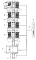
本実施例1の電子部品実装基板生産ラインは、基板11を搬送する搬送コンベア12(搬送経路)に沿って、印刷装置13と複数台の電子部品実装装置14〜17が一列に配置されている。印刷装置13と各電子部品実装装置14〜17には、半田印刷状態や電子部品実装状態の良否を画像処理により検査するために、カメラ(図示せず)が搭載されている。各電子部品実装装置14〜17のカメラは、装着ヘッドに取り付けても良いし、装置天井部等に取り付けても良い。また、各カメラは、2次元カメラ単体又はラインセンサカメラであっても良いし、複数のカメラの合成画像を得る撮像系で構成しても良い。各カメラの視野は、できるだけ広い方が良く、基板11全体を一望視できる広視野のカメラが最も望ましい。
A first embodiment of the present invention will be described with reference to FIGS.
First, an example of an electronic component mounting board production line will be schematically described with reference to FIG.
In the electronic component mounting board production line of the first embodiment, a
この電子部品実装基板生産ラインを構成する印刷装置13、電子部品実装装置14〜17、カメラ、搬送コンベア12は、それぞれネットワーク18を介して生産制御コンピュータ19に接続されている。この生産制御コンピュータ19は、各装置13〜17のカメラで撮像した画像を前後2つの装置間で比較して差分画像を求め、その差分画像に基づいて当該装置13〜17で作業が正常に行われたか否かを検査する。
The
本実施例1の画像処理は、原則として仮想画面上で行う。従来の画像処理では、視野内の有限個の画素(ピクセル)上で、行っていたが、そのような格子状の画面では、微小な移動や回転を考えることは非常に困難である。そこで、本実施例1では、基本的に仮想画面で画像処理するようにしている。ここで、仮想画面とは、無限個の画素を有する画面のことである。この考え方は現実的ではないので、次の方法を採用する。 In principle, the image processing of the first embodiment is performed on a virtual screen. Conventional image processing is performed on a finite number of pixels (pixels) in the field of view, but it is very difficult to consider minute movement and rotation on such a grid-like screen. Therefore, in the first embodiment, image processing is basically performed on a virtual screen. Here, the virtual screen is a screen having an infinite number of pixels. Since this idea is not realistic, the following method is adopted.
図2において、任意の仮想点eの輝度又は色調(以下これらを単に「輝度」という)を求める際に、その仮想点eの近傍の4画素a〜dの輝度を2次元線形補間して、仮想点eの輝度を求める。以下の説明は、画素を超越した仮想画面上で処理するものとして行う。ただし、本発明は、仮想画面上で画像処理することを必須要件とするものではない。 In FIG. 2, when obtaining the luminance or tone of an arbitrary virtual point e (hereinafter simply referred to as “luminance”), the luminance of the four pixels a to d in the vicinity of the virtual point e is two-dimensionally linearly interpolated, The brightness of the virtual point e is obtained. In the following description, processing is performed on a virtual screen that transcends pixels. However, the present invention does not necessarily require image processing on a virtual screen.
ところで、前後2つの装置間で正確な差分画像を得るためには、前後2つの装置の画像間で撮像条件が正確に一致する必要があるが、実際には、各装置13〜17におけける基板11とカメラとの間の位置決め誤差やカメラの固体差、分解能、照明(光学系)のばらつき等によって各装置13〜17のカメラで撮像した画像にずれが生じるため、前後2つの装置間で正確な差分画像を得ることは困難である。差分画像の精度が悪ければ、半田印刷状態や電子部品実装状態の検査精度が悪くなる。
By the way, in order to obtain an accurate difference image between the two front and rear devices, it is necessary to accurately match the imaging conditions between the images of the two front and rear devices. Since the images captured by the cameras of the
前後2つの装置間の画像のずれは、撮像部位のXY方向の位置ずれ、傾き及び撮像倍率の差の3種類のずれ(差)があるため、本実施例1では、これら3種類のずれを「オフセット量」として求めて、前後2つの装置の画像間で前記オフセット量を考慮して両画像の差分をとる画素(相当点D1 ,D2 )の対応位置関係を決定して差分画像を求めるようにしている。 There are three types of shifts (differences) between the front and rear devices, namely, the positional shift in the X and Y directions of the imaging region, the difference between the tilt and the imaging magnification. Therefore, in the first embodiment, these three types of shifts are detected. By obtaining the “offset amount”, the corresponding positional relationship between the pixels (corresponding points D1, D2) that take the difference between the two images in consideration of the offset amount between the images of the two front and rear devices is determined to obtain the difference image. I have to.
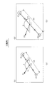
この場合、オフセット量を演算する際に、図3(a),(b)に示すように、2つの画像G1 ,G2 からそれぞれ2個の基準点(A1 ,B1 )、(A2 ,B2 )を認識し、各画像G1 ,G2 の2個の基準点(A1 ,B1 )間、(A2 ,B2 )間を結ぶ直線上の特定点C1 ,C2 のXY座標と該直線の長さm1 ,m2 と傾きθ1 ,θ2 に基づいてオフセット量を演算する。 In this case, when calculating the offset amount, as shown in FIGS. 3A and 3B, two reference points (A1, B1), (A2, B2) are respectively obtained from the two images G1, G2. XY coordinates of specific points C1, C2 on the straight line connecting the two reference points (A1, B1) and (A2, B2) of each image G1, G2, and the lengths m1, m2 of the straight line The offset amount is calculated based on the inclinations θ1 and θ2.
ここで、基準点(A1 ,B1 )、(A2 ,B2 )は、基板11の表面に形成された基準位置認識マークを用いても良いし、或は、基板11に形成された特定の導体パターン等によって決定される点であっても良い。
Here, as the reference points (A1, B1), (A2, B2), a reference position recognition mark formed on the surface of the
また、2個の基準点(A1 ,B1 )間、(A2 ,B2 )間を結ぶ直線上の特定点C1 ,C2 は、例えば、該直線の中点又はいずれか一方の基準点であっても良い。要は、2個の基準点(A1 ,B1 )間、(A2 ,B2 )間を結ぶ直線上の決められた位置に特定点C1 ,C2 を設定すれば良い。以下の説明では、直線の中点を特定点C1 ,C2 とした例で説明する。 Also, the specific points C1 and C2 on the straight line connecting the two reference points (A1, B1) and (A2, B2) may be, for example, the midpoint of the straight line or one of the reference points. good. In short, the specific points C1 and C2 may be set at predetermined positions on a straight line connecting the two reference points (A1, B1) and (A2, B2). In the following description, an example in which the midpoint of the straight line is the specific points C1 and C2 will be described.
2個の基準点(A1 ,B1 )、(A2 ,B2 )は、パターンマッチング等により別々に正確な座標(X,Y)を求めることができる。カメラの視野より広い画像の差分画像を得たい場合は、カメラの撮像エリアを少しオーバラップさせて変更して、複数枚の画像を取り込んで1枚の画像につなぎ合わせるようにすれば良い。 For the two reference points (A1, B1) and (A2, B2), accurate coordinates (X, Y) can be obtained separately by pattern matching or the like. In order to obtain a differential image of an image wider than the field of view of the camera, the imaging area of the camera may be slightly overlapped and changed so as to capture a plurality of images and join them into one image.
差分画像を得るポイントは、2つの画像G1 ,G2 の対応する任意の仮想点(物理的な画素を超越した点)D1 ,D2 どうしの輝度及び/又は色調の差分を求めることである。ここで、対応する任意の仮想点D1 ,D2 を「相当点」と呼ぶことにする。一方の相当点D1 は、他方の相当点D2 でもある。 The point of obtaining the difference image is to obtain a difference in luminance and / or color tone between arbitrary virtual points (points exceeding physical pixels) D1 and D2 corresponding to the two images G1 and G2. Here, the corresponding arbitrary virtual points D1 and D2 are referred to as “equivalent points”. One equivalent point D1 is also the other equivalent point D2.
カメラの視野内の全ての点について、相当点D1 ,D2 どうしの差分値を得て、2次元画像を作ると、それが差分画面となる。比較画像処理を行うには、差分画面を全て作成してから行う必要はない。差分画面の画像処理したい点又はエリアについて、差分画面を求めてから画像処理する方が、処理時間を節約できる場合がある。 When a difference value between corresponding points D1 and D2 is obtained for all points in the field of view of the camera and a two-dimensional image is created, it becomes a difference screen. In order to perform the comparison image processing, it is not necessary to perform the processing after all the difference screens are created. In some cases, it may be possible to save processing time by performing image processing after obtaining a difference screen for a point or an area to be subjected to image processing on the difference screen.
相当点D1 ,D2 と特定点C1 ,C2 との間の距離n1 ,n2 は、次式の関係が成立する。
n2 =n1 ×(m2 /m1 )
ここで、m1 ,m2 は、2個の基準点(A1 ,B1 )間、(A2 ,B2 )間を結ぶ直線の長さである。
相当点D1 ,D2 は、特定点C1 ,C2 から距離n1 ,n2 だけ離れた位置で、且つ、各直線(A1 −B1 )、(A2 −B2 )に対する傾きφが同じとなる点である。
The distances n1 and n2 between the corresponding points D1 and D2 and the specific points C1 and C2 have the following relationship.
n2 = n1 x (m2 / m1)
Here, m1 and m2 are the lengths of straight lines connecting the two reference points (A1, B1) and (A2, B2).
The equivalent points D1 and D2 are points that are separated from the specific points C1 and C2 by the distances n1 and n2, and have the same inclination φ with respect to the straight lines (A1−B1) and (A2−B2).
また、各画像G1 ,G2 のX軸に対する各直線(A1 −B1 )、(A2 −B2 )の傾きをθ1 ,θ2 とすると、一方の画像G1 の相当点D1 は、X軸に対する傾きがθ1 +φとなり、他方の画像G2 の相当点D2 は、X軸に対する傾きがθ2 +φとなる。このような幾何学的な関係を利用して、一方の画像G1 の相当点D1 に対応する他方の画像G2 の相当点D2 を幾何学的に算出することができる。これにより、前後2つの装置の画像G1 ,G2 間でオフセット量(撮像部位のXY方向の位置ずれ、傾き及び撮像倍率の差)を考慮して両画像G1 ,G2 の差分をとる画素(相当点D1 ,D2 )の対応位置関係を決定して正確な差分画像を求めることができる。 Further, if the inclinations of the straight lines (A1−B1) and (A2−B2) with respect to the X axis of the images G1 and G2 are θ1 and θ2, the corresponding point D1 of one image G1 has an inclination with respect to the X axis of θ1 + φ. The equivalent point D2 of the other image G2 has an inclination with respect to the X axis of θ2 + φ. By using such a geometric relationship, the equivalent point D2 of the other image G2 corresponding to the equivalent point D1 of one image G1 can be geometrically calculated. As a result, a pixel (corresponding point) that takes the difference between the two images G1 and G2 in consideration of the offset amount (difference in position and inclination in the X and Y directions of the imaging region and the difference in imaging magnification) between the images G1 and G2 of the two front and rear devices. D1 and D2) can be determined to obtain an accurate difference image.
前述したように、特定点C1 ,C2 は、各直線(A1 −B1 )、(A2 −B2 )の中点に限定されず、いずれか一方の基準点を用いても良く、この場合でも、上記と同様の幾何学的な手法で相当点D1 ,D2 を算出することができる。従って、各画像G1 ,G2 内の離れた位置に2個の基準点を特定できれば、幾何学的な手法で相当点D1 ,D2 を算出することができる。そして、2個の基準点間の距離(直線の長さ)が長くなるほど、相当点D1 ,D2 の算出精度を高めることができる。 As described above, the specific points C1 and C2 are not limited to the midpoints of the straight lines (A1 -B1) and (A2 -B2), and either one of the reference points may be used. The corresponding points D1 and D2 can be calculated by the same geometrical method. Accordingly, if two reference points can be specified at positions distant from each other in the images G1 and G2, the corresponding points D1 and D2 can be calculated by a geometric method. The calculation accuracy of the corresponding points D1 and D2 can be increased as the distance between the two reference points (the length of the straight line) increases.
以上説明した本実施例1では、電子部品実装基板生産ラインの生産制御コンピュータ19は、前後2つの装置の画像G1 ,G2 間でオフセット量(撮像部位のXY方向の位置ずれ、傾き及び撮像倍率の差)を演算するオフセット量演算手段として機能すると共に、前後2つの装置の画像G1 ,G2 間で前記オフセット量を考慮して両画像G1 ,G2 の差分をとる画素(相当点D1 ,D2 )の対応位置関係を決定して、両画像G1 ,G2 の全ての点(画素)について、相当点D1 ,D2 どうしの差分値を得て差分画像を求める差分画像演算手段として機能し、この差分画像に基づいて当該装置で作業が正常に行われたか否かを検査する。これにより、前後2つの装置間で画像のずれがない精度の良い差分画像を求めることが可能となり、半田印刷状態や電子部品実装状態の良否を精度良く検査することができる。
In the first embodiment described above, the
上記実施例1では、2個の基準点(A1 ,B1 )、(A2 ,B2 )からオフセット量を演算するようにしたが、図4(a)、(b)に示す本発明の実施例2では、前後2つの装置の画像G1 ,G2 からそれぞれ非円形の特定形状M1 ,M2 を認識して、各画像G1 ,G2 の特定形状M1 ,M2 から決定される基準点C1 ,C2 のXY座標と該特定形状M1 ,M2 のサイズと傾きθ1 ,θ2 に基づいてオフセット量を演算するようにしている。 In the first embodiment, the offset amount is calculated from the two reference points (A1, B1) and (A2, B2), but the second embodiment of the present invention shown in FIGS. 4 (a) and 4 (b). Then, the non-circular specific shapes M1 and M2 are recognized from the images G1 and G2 of the two front and rear devices, respectively, and the XY coordinates of the reference points C1 and C2 determined from the specific shapes M1 and M2 of the images G1 and G2 and An offset amount is calculated on the basis of the sizes and inclinations θ1 and θ2 of the specific shapes M1 and M2.
ここで、非円形の特定形状M1 ,M2 は、基板11の表面に形成された基準位置認識用の大型のマークを用いても良いし、或は、基板11に形成された特定形状の導体パターン等を用いて良く、また、特定形状M1 ,M2 の形状も、八角形等の多角形に限定されず、コ字形のような形状であっても良く、要は、位置と傾きとサイズを求めることができる方向性のある形状であれば良い。特定形状M1 ,M2 は、画像G1 ,G2 内で大きくなるほど、後述する相当点D1 ,D2 の算出精度が高くなる。
Here, as the non-circular specific shapes M1 and M2, a large mark for reference position recognition formed on the surface of the
各画像G1 ,G2 の特定形状M1 ,M2 から決定される基準点C1 ,C2 のXY座標の差から撮像部位のXY方向の位置ずれが求められ、特定形状M1 ,M2 のサイズの比から撮像倍率の差が求められ、特定形状M1 ,M2 の傾きθ1 ,θ2 の差から撮像部位の傾きの差が求められる。 The positional deviation in the XY direction of the imaging region is obtained from the difference in the XY coordinates of the reference points C1 and C2 determined from the specific shapes M1 and M2 of the images G1 and G2, and the imaging magnification is determined from the ratio of the sizes of the specific shapes M1 and M2. The difference between the inclinations of the imaging parts is obtained from the difference between the inclinations θ1 and θ2 of the specific shapes M1 and M2.
特定形状M1 ,M2 の基準点C1 ,C2 は、例えば、該特定形状M1 ,M2 の中心又は図心に設定しても良く、要は、特定形状M1 ,M2 から一義的に決定される位置に基準点C1 ,C2 を設定すれば良い。例えば、特定形状M1 ,M2 の中心を基準点C1 ,C2 とする場合は、特定形状M1 ,M2 のX軸方向中心線Lx1,Lx2と、Y軸方向中心線Ly1,Ly2を求め、両中心線の交点を特定形状M1 ,M2 の中心とし、この中心を基準点C1 ,C2 とすれば良い。 The reference points C1 and C2 of the specific shapes M1 and M2 may be set, for example, at the centers or centroids of the specific shapes M1 and M2. In short, the points are uniquely determined from the specific shapes M1 and M2. Reference points C1 and C2 may be set. For example, when the centers of the specific shapes M1 and M2 are set as the reference points C1 and C2, the X-axis direction center lines Lx1 and Lx2 and the Y-axis direction center lines Ly1 and Ly2 of the specific shapes M1 and M2 are obtained. Is the center of the specific shapes M1 and M2, and these centers may be used as the reference points C1 and C2.
また、特定形状M1 ,M2 のサイズは、特定形状M1 ,M2 の外形寸法をX軸方向中心線Lx1,Lx2又はY軸方向中心線Ly1,Ly2に沿って計測し、その計測値をサイズとすれば良い。 The sizes of the specific shapes M1 and M2 are determined by measuring the external dimensions of the specific shapes M1 and M2 along the X-axis direction center lines Lx1 and Lx2 or the Y-axis direction center lines Ly1 and Ly2. It ’s fine.
また、特定形状M1 ,M2 の傾きθ1 ,θ2 は、各画像G1 ,G2 のY軸に対するY軸方向中心線Ly1,Ly2の傾きを求めたり、或は、X軸に対するX軸方向中心線Lx1,Lx2の傾きを求めれば良い。 The inclinations θ1 and θ2 of the specific shapes M1 and M2 determine the inclinations of the Y axis direction center lines Ly1 and Ly2 with respect to the Y axis of the images G1 and G2, or the X axis direction center lines Lx1 and Lx with respect to the X axis. What is necessary is just to obtain | require the inclination of Lx2.
そして、各画像G1 ,G2 の特定形状M1 ,M2 から決定される基準点C1 ,C2 のXY座標と該特定形状M1 ,M2 のサイズと傾きθ1 ,θ2 に基づいてオフセット量を演算した後、前記実施例1と同様の幾何学的手法で、前後2つの装置の画像G1 ,G2 間で前記オフセット量を考慮して両画像G1 ,G2 の差分をとる画素(相当点D1 ,D2 )の対応位置関係を決定して、両画像G1 ,G2 の全ての点(画素)について相当点D1 ,D2 どうしの差分値を得て差分画像を求め、この差分画像に基づいて当該装置で作業が正常に行われたか否かを検査する。これにより、前後2つの装置間で画像のずれがない精度の良い差分画像を求めることが可能となり、半田印刷状態や電子部品実装状態の良否を精度良く検査することができる。 Then, after calculating the offset amount based on the XY coordinates of the reference points C1 and C2 determined from the specific shapes M1 and M2 of the images G1 and G2, and the sizes and inclinations θ1 and θ2 of the specific shapes M1 and M2, respectively. Corresponding positions of pixels (corresponding points D1, D2) that take the difference between the two images G1, G2 in consideration of the offset amount between the images G1, G2 of the two front and rear devices by the same geometric method as in the first embodiment. The relationship is determined, the difference value between the corresponding points D1 and D2 is obtained for all points (pixels) of both images G1 and G2, and a difference image is obtained. Based on the difference image, the operation is normally performed in the apparatus. Inspect whether or not As a result, it is possible to obtain an accurate difference image with no image shift between the two front and rear devices, and it is possible to accurately inspect the quality of the solder printing state and the electronic component mounting state.
尚、本発明は、基板への半田印刷、電子部品の実装、基板の検査のうちの少なくとも1つを実行する生産ラインに適用して実施でき、また、生産ラインを構成する複数の装置の全てにカメラを設けた構成に限定されず、生産ラインを構成する複数の装置のうちの2つ以上の装置にそれぞれカメラを設けた構成としても良い。 The present invention can be applied to a production line that executes at least one of solder printing on a substrate, mounting of electronic components, and inspection of the substrate, and all of a plurality of apparatuses constituting the production line. However, the present invention is not limited to the configuration in which the camera is provided, and a configuration in which the camera is provided in each of two or more of the plurality of devices constituting the production line may be employed.
11…基板、12…搬送コンベア(搬送経路)、13…印刷装置、14〜17…電子部品実装装置、18…ネットワーク、19…生産制御コンピュータ(オフセット量演算手段,差分画像演算手段)
DESCRIPTION OF
Claims (8)
前後2つの装置の画像間で撮像部位のXY方向の位置ずれ、傾き及び撮像倍率の差(以下これらを「オフセット量」と総称する)を演算するオフセット量演算手段と、
前後2つの装置の画像間で前記オフセット量を考慮して両画像の差分をとる画素の対応位置関係を決定して差分画像を求める差分画像演算手段と
を備え、
前記オフセット量演算手段は、各画像からそれぞれ非円形の特定形状を認識し、各画像の特定形状から決定される基準点のXY座標と該特定形状のサイズと傾きに基づいて前記オフセット量を演算することを特徴とする生産ラインの検査システム。 A plurality of devices are arranged along the substrate conveyance path, and two or more of these devices are each provided with a camera that images the substrate. In a production line inspection system for inspecting whether or not work has been normally performed on the apparatus based on the difference image,
An offset amount calculation means for calculating a difference in position, inclination, and imaging magnification of the imaging region between the images of the two front and rear devices (hereinafter collectively referred to as “offset amount”);
A differential image calculation means for determining a corresponding positional relationship between pixels taking a difference between the two images in consideration of the offset amount between the images of the two front and rear devices and obtaining a differential image ;
The offset amount calculation means recognizes a non-circular specific shape from each image, and calculates the offset amount based on the XY coordinates of the reference point determined from the specific shape of each image and the size and inclination of the specific shape A production line inspection system characterized by
前記差分画像を求める際に、前後2つの装置の画像間で撮像部位のXY方向の位置ずれ、傾き及び撮像倍率の差(以下これらを「オフセット量」と総称する)を演算し、前後2つの装置の画像間で前記オフセット量を考慮して両画像の差分をとる画素の対応位置関係を決定して差分画像を求め、
前記オフセット量を演算する際に、各画像からそれぞれ非円形の特定形状を認識し、各画像の特定形状から決定される基準点のXY座標と該特定形状のサイズと傾きに基づいて前記オフセット量を演算することを特徴とする生産ラインの検査方法。 A plurality of devices are arranged along the substrate conveyance path, and two or more of these devices are each provided with a camera that images the substrate. In a production line inspection method for inspecting whether or not work has been normally performed on the apparatus based on the difference image, by comparing between
When obtaining the difference image, the difference between the positional shift, the tilt and the imaging magnification (hereinafter collectively referred to as “offset amount”) of the imaging part between the images of the two front and rear devices is calculated, Taking into account the offset amount between the images of the device, determine the corresponding positional relationship of the pixels that take the difference between the two images to obtain a difference image ,
When calculating the offset amount, the non-circular specific shape is recognized from each image, and the offset amount is based on the XY coordinates of the reference point determined from the specific shape of each image and the size and inclination of the specific shape. A production line inspection method characterized by calculating
Priority Applications (1)
| Application Number | Priority Date | Filing Date | Title |
|---|---|---|---|
| JP2007101433A JP4900951B2 (en) | 2007-04-09 | 2007-04-09 | Production line inspection system and inspection method |
Applications Claiming Priority (1)
| Application Number | Priority Date | Filing Date | Title |
|---|---|---|---|
| JP2007101433A JP4900951B2 (en) | 2007-04-09 | 2007-04-09 | Production line inspection system and inspection method |
Publications (2)
| Publication Number | Publication Date |
|---|---|
| JP2008258519A JP2008258519A (en) | 2008-10-23 |
| JP4900951B2 true JP4900951B2 (en) | 2012-03-21 |
Family
ID=39981767
Family Applications (1)
| Application Number | Title | Priority Date | Filing Date |
|---|---|---|---|
| JP2007101433A Active JP4900951B2 (en) | 2007-04-09 | 2007-04-09 | Production line inspection system and inspection method |
Country Status (1)
| Country | Link |
|---|---|
| JP (1) | JP4900951B2 (en) |
Families Citing this family (2)
| Publication number | Priority date | Publication date | Assignee | Title |
|---|---|---|---|---|
| CN112559314A (en) * | 2019-09-26 | 2021-03-26 | 上海汽车集团股份有限公司 | Testing method and testing device for human-computer interaction interface |
| WO2024062635A1 (en) * | 2022-09-23 | 2024-03-28 | 株式会社Fuji | Testing device and testing method |
Family Cites Families (5)
| Publication number | Priority date | Publication date | Assignee | Title |
|---|---|---|---|---|
| JP3994925B2 (en) * | 2003-06-02 | 2007-10-24 | オムロン株式会社 | Display method, quality control device, and quality control system |
| JP3857668B2 (en) * | 2003-07-11 | 2006-12-13 | 日本アビオニクス株式会社 | Pattern alignment method |
| US20050209822A1 (en) * | 2004-03-01 | 2005-09-22 | Masato Ishiba | Inspection method and system and production method of mounted substrate |
| JP4165538B2 (en) * | 2004-07-21 | 2008-10-15 | オムロン株式会社 | Component mounting inspection method and component mounting inspection device |
| JP4612484B2 (en) * | 2005-06-21 | 2011-01-12 | 株式会社図研 | Substrate inspection result analysis support method, board inspection result analysis support apparatus and program using this method |
-
2007
- 2007-04-09 JP JP2007101433A patent/JP4900951B2/en active Active
Also Published As
| Publication number | Publication date |
|---|---|
| JP2008258519A (en) | 2008-10-23 |
Similar Documents
| Publication | Publication Date | Title |
|---|---|---|
| TWI651578B (en) | Image capturing device | |
| US9418435B2 (en) | Three-dimensional measurement method | |
| US8886350B2 (en) | Displacement calculation method, drawing data correction method, substrate manufacturing method, and drawing apparatus | |
| US20130278723A1 (en) | Three-dimensional measurement system and three-dimensional measurement method | |
| JP6209833B2 (en) | Inspection tool, inspection method, stereo camera production method and system | |
| US9423242B2 (en) | Board-warping measuring apparatus and board-warping measuring method thereof | |
| JP2008185514A (en) | Substrate visual inspection apparatus | |
| WO2020065850A1 (en) | Three-dimensional measuring device | |
| US10841561B2 (en) | Apparatus and method for three-dimensional inspection | |
| WO2018171031A1 (en) | Method for matching feature points of three-camera group, measurement method and three-dimensional detection apparatus | |
| KR101183101B1 (en) | Method of die bonding for flip chip | |
| JP4900951B2 (en) | Production line inspection system and inspection method | |
| JP4405009B2 (en) | Calibration method of inspection machine with line sensor camera | |
| US7440080B2 (en) | Method and apparatus for automatic correction of direct exposure apparatus | |
| JP2012033829A (en) | Component mounting machine and image processing method | |
| CN113390894A (en) | Substrate measuring system and method thereof | |
| JP4915940B2 (en) | Image processing data creation method and image processing data creation device | |
| JP3291176B2 (en) | Circuit pattern inspection method and inspection device | |
| JP4970101B2 (en) | Defect detection method | |
| JP5271654B2 (en) | Electronic component mounting equipment | |
| JPH11132735A (en) | Ic lead floating inspection device and inspection method | |
| KR20150076544A (en) | Method of reviewing defect of substrate | |
| JP4269258B2 (en) | Method for aligning exposure mask and inner layer substrate | |
| WO2023032962A1 (en) | Direct-drawing device and method for controlling the same | |
| JP2009170586A (en) | Method and apparatus for recognizing electronic component |
Legal Events
| Date | Code | Title | Description |
|---|---|---|---|
| A621 | Written request for application examination |
Free format text: JAPANESE INTERMEDIATE CODE: A621 Effective date: 20100318 |
|
| A977 | Report on retrieval |
Free format text: JAPANESE INTERMEDIATE CODE: A971007 Effective date: 20111020 |
|
| A131 | Notification of reasons for refusal |
Free format text: JAPANESE INTERMEDIATE CODE: A131 Effective date: 20111024 |
|
| A521 | Request for written amendment filed |
Free format text: JAPANESE INTERMEDIATE CODE: A523 Effective date: 20111124 |
|
| TRDD | Decision of grant or rejection written | ||
| A01 | Written decision to grant a patent or to grant a registration (utility model) |
Free format text: JAPANESE INTERMEDIATE CODE: A01 Effective date: 20111226 |
|
| A01 | Written decision to grant a patent or to grant a registration (utility model) |
Free format text: JAPANESE INTERMEDIATE CODE: A01 |
|
| A61 | First payment of annual fees (during grant procedure) |
Free format text: JAPANESE INTERMEDIATE CODE: A61 Effective date: 20111226 |
|
| R150 | Certificate of patent or registration of utility model |
Ref document number: 4900951 Country of ref document: JP Free format text: JAPANESE INTERMEDIATE CODE: R150 Free format text: JAPANESE INTERMEDIATE CODE: R150 |
|
| FPAY | Renewal fee payment (event date is renewal date of database) |
Free format text: PAYMENT UNTIL: 20150113 Year of fee payment: 3 |
|
| R250 | Receipt of annual fees |
Free format text: JAPANESE INTERMEDIATE CODE: R250 |
|
| R250 | Receipt of annual fees |
Free format text: JAPANESE INTERMEDIATE CODE: R250 |
|
| R250 | Receipt of annual fees |
Free format text: JAPANESE INTERMEDIATE CODE: R250 |
|
| R250 | Receipt of annual fees |
Free format text: JAPANESE INTERMEDIATE CODE: R250 |
|
| S533 | Written request for registration of change of name |
Free format text: JAPANESE INTERMEDIATE CODE: R313533 |
|
| R350 | Written notification of registration of transfer |
Free format text: JAPANESE INTERMEDIATE CODE: R350 |
|
| R250 | Receipt of annual fees |
Free format text: JAPANESE INTERMEDIATE CODE: R250 |
|
| R250 | Receipt of annual fees |
Free format text: JAPANESE INTERMEDIATE CODE: R250 |
|
| R250 | Receipt of annual fees |
Free format text: JAPANESE INTERMEDIATE CODE: R250 |
|
| R250 | Receipt of annual fees |
Free format text: JAPANESE INTERMEDIATE CODE: R250 |
|
| R250 | Receipt of annual fees |
Free format text: JAPANESE INTERMEDIATE CODE: R250 |
|
| R250 | Receipt of annual fees |
Free format text: JAPANESE INTERMEDIATE CODE: R250 |