JP4900623B2 - Compound balun - Google Patents
Compound balun Download PDFInfo
- Publication number
- JP4900623B2 JP4900623B2 JP2009126349A JP2009126349A JP4900623B2 JP 4900623 B2 JP4900623 B2 JP 4900623B2 JP 2009126349 A JP2009126349 A JP 2009126349A JP 2009126349 A JP2009126349 A JP 2009126349A JP 4900623 B2 JP4900623 B2 JP 4900623B2
- Authority
- JP
- Japan
- Prior art keywords
- line
- coupled
- balun
- coupling line
- dielectric layer
- Prior art date
- Legal status (The legal status is an assumption and is not a legal conclusion. Google has not performed a legal analysis and makes no representation as to the accuracy of the status listed.)
- Active
Links
Images


Landscapes
- Coils Or Transformers For Communication (AREA)
Description
本発明は、平衡伝送線路と不平衡伝送線路とを結合する複合バランに関するものである。 The present invention relates to a composite balun that combines a balanced transmission line and an unbalanced transmission line.
従来より、高周波回路における伝送線路の平衡−不平衡変換器として、チップ状の積層型バランが知られている。バランは、通常、一対の平衡伝送線路を構成する第1及び第2線路部と、この平衡伝送線路に電磁結合する一つの不平衡伝送線路を構成する第3及び第4線路部と、グランド電極と、複数の誘電体シートとを積み重ねて構成した積層体を備えている。そして、第1線路部と第3線路部が誘電体シートを挟んで対向する部分で電磁結合して結合器を構成し、同様に、第2線路部と第4線路部が誘電体シートを挟んで対向する部分で電磁結合して結合器を構成する。 Conventionally, a chip-shaped laminated balun is known as a balanced-unbalanced converter of a transmission line in a high-frequency circuit. The balun usually includes a first and second line portions that constitute a pair of balanced transmission lines, a third and fourth line portions that constitute one unbalanced transmission line that is electromagnetically coupled to the balanced transmission lines, and a ground electrode. And a laminated body formed by stacking a plurality of dielectric sheets. The first line portion and the third line portion are electromagnetically coupled to each other at a portion facing each other across the dielectric sheet to form a coupler. Similarly, the second line portion and the fourth line portion sandwich the dielectric sheet. The coupler is configured by electromagnetic coupling at the opposing portions.
ところが、従来の積層型バランは、一つのチップに一つのバランしか内蔵していなかったため、例えば、複数のバランを携帯電話などの移動体通信機、無線LANなどに組み込む必要がある場合には、複数個分の実装面積をプリント基板上に確保する必要があった。従って、通信機の大型化を招くという問題があった。 However, since the conventional stacked balun had only one balun built in one chip, for example, when it is necessary to incorporate a plurality of baluns into a mobile communication device such as a mobile phone, a wireless LAN, etc. It was necessary to secure a plurality of mounting areas on the printed circuit board. Therefore, there has been a problem that the communication apparatus is increased in size.
上述した問題点を解決する試みは既になされている。例えば、特許文献1は、複数のバランを備え、バランのそれぞれが、一対の平衡伝送線路と、一対の平衡伝送線路に誘電体層を介して電磁結合する一つの不平衡伝送線路と、平衡伝送線路及び不平衡伝送線路の少なくともいずれか一方の伝送線路に誘電体層を介して対置しているグランド電極と、複数の誘電体層とを積み重ねて構成された積層型複合バランを開示している。
Attempts have already been made to solve the above-mentioned problems. For example,
ところで、複合バランを移動体通信機の電力増幅器PAの前段に挿入し、電力増幅器に対する差動入力を予めバランから供給する場合や、複合バランを無線周波数集積回路RFICの後段に配置し、バランを介して無線周波数集積回路RFICに電源を供給する場合は、複合バランを通して、電力増幅器PAや、無線周波数集積回路RFICに直流電圧を供給する必要がある。特許文献1には、そのような要求を満たすための構成が開示されていない。また、複合バランを通して、電力増幅器PAや、無線周波数集積回路RFICに直流電圧を供給するとすれば、電源供給回路を経由して侵入するノイズに対する対策が必要であるところ、そのような手段についても、特許文献1には開示するところがない。
By the way, when the composite balun is inserted in the front stage of the power amplifier PA of the mobile communication device and the differential input to the power amplifier is supplied from the balun in advance, the composite balun is arranged in the subsequent stage of the radio frequency integrated circuit RFIC, and the balun is When the power is supplied to the radio frequency integrated circuit RFIC via the DC voltage, it is necessary to supply a DC voltage to the power amplifier PA and the radio frequency integrated circuit RFIC through the composite balun.
本発明の課題は、電力増幅器や、無線周波数集積回路に直流電圧を供給する必要がある場合に有用な複合バランを提供することである。 An object of the present invention is to provide a composite balun that is useful when a DC voltage needs to be supplied to a power amplifier or a radio frequency integrated circuit.
本発明のもう一つの課題は、電力増幅器や、無線周波数集積回路に直流電圧を供給する必要がある場合に、電源供給回路を経由して侵入するノイズに対する対策を施した複合バランを提供することである。 Another object of the present invention is to provide a composite balun that takes measures against noise that enters through a power supply circuit when a DC voltage needs to be supplied to a power amplifier or a radio frequency integrated circuit. It is.
上述した課題を解決するため、本発明に係る複合バランは、複数個のバランと、少なくとも1つのキャパシタと、直流電圧供給端子とを含む。前記複数個のバラン及び前記キャパシタは、1つのチップ内に内蔵されている。前記バランのそれぞれは、第1乃至第4結合線路と、第1平衡端子と、第2平衡端子と、不平衡端子とを含んでいる。前記第1結合線路は、一端が前記不平衡端子に接続されており、前記第2結合線路は、一端が前記第1結合線路の他端に接続されている。前記第3結合線路は、前記第1結合線路に電磁結合し、一端が前記第1平衡端子に接続され、他端が前記直流電圧供給端子に接続されており、前記第4結合線路は、前記第2結合線路に電磁結合し、一端が前記第2平衡端子に接続され、他端が前記直流電圧供給端子に接続されている。前記キャパシタは、一端が、前記直流電圧供給端子に接続され、他端が接地端子に導かれている。 In order to solve the above-described problem, a composite balun according to the present invention includes a plurality of baluns, at least one capacitor, and a DC voltage supply terminal. The plurality of baluns and the capacitor are built in one chip. Each of the baluns includes first to fourth coupled lines, a first balanced terminal, a second balanced terminal, and an unbalanced terminal. One end of the first coupled line is connected to the unbalanced terminal, and one end of the second coupled line is connected to the other end of the first coupled line. The third coupled line is electromagnetically coupled to the first coupled line, one end is connected to the first balanced terminal, the other end is connected to the DC voltage supply terminal, and the fourth coupled line is The second coupling line is electromagnetically coupled, one end is connected to the second balanced terminal, and the other end is connected to the DC voltage supply terminal. One end of the capacitor is connected to the DC voltage supply terminal, and the other end is led to a ground terminal.
上述したように、本発明に係る複合バランは、その主要部である複数個のバランは、1つのチップ内に内蔵されているから、複数のバランを携帯電話などの移動体通信機、無線LANなどに組み込む場合には、1数個分の実装面積をプリント基板上に確保すればよく、小型化の要請に応えることができる。 As described above, in the composite balun according to the present invention, a plurality of baluns, which are the main parts, are built in one chip. In the case of incorporating into a circuit board, etc., it is sufficient to secure a mounting area for one or more pieces on a printed circuit board, and it is possible to meet the demand for downsizing.
複数のバランのそれぞれにおいて、第1結合線路は、一端が不平衡端子に接続されており、第2結合線路は、一端が第1結合線路の他端に接続されており、第3結合線路は、第1結合線路に電磁結合し、一端が第1平衡端子に接続され、第4結合線路は、第2結合線路に電磁結合し、一端が第2平衡端子に接続されているから、第3及び第4結合線路を平衡伝送線路とし、第1及び第2結合線路を不平衡伝送線路とする複合バランが得られる。 In each of the plurality of baluns, one end of the first coupled line is connected to the unbalanced terminal, one end of the second coupled line is connected to the other end of the first coupled line, and the third coupled line is Since the first coupling line is electromagnetically coupled, one end is connected to the first balanced terminal, the fourth coupled line is electromagnetically coupled to the second coupled line, and one end is connected to the second balanced terminal, the third In addition, a composite balun is obtained in which the fourth coupled line is a balanced transmission line and the first and second coupled lines are unbalanced transmission lines.
第3結合線路は、他端が直流電圧供給端子に接続されており、第4結合線路は他端が直流電圧供給端子に接続されているから、電力増幅器や、無線周波数集積回路に直流電圧を供給する必要がある場合に、複合バランを通して直流電圧を供給しえる使い勝手のよい複合バランが得られる。 Since the other end of the third coupled line is connected to the DC voltage supply terminal and the other end of the fourth coupled line is connected to the DC voltage supply terminal, the DC voltage is applied to the power amplifier or the radio frequency integrated circuit. When it is necessary to supply, a user-friendly composite balun that can supply a DC voltage through the composite balun is obtained.
更に、一端が直流電圧供給端子に接続され、他端が接地端子に導かれているキャパシタを含んでいるから、電源供給回路を経由して侵入するノイズをキャパシタによって吸収し得る。しかも、このキャパシタは、複数個のバランと共に、1つのチップ内に内蔵されているから、複合バランにキャパシタを外付けする場合と対比して、ユーザ側の実装作業が容易になるとともに、回路基板上で見た実装面積が縮小される。 Further, since the capacitor includes a capacitor having one end connected to the DC voltage supply terminal and the other end guided to the ground terminal, noise entering through the power supply circuit can be absorbed by the capacitor. In addition, since this capacitor is built in one chip together with a plurality of baluns, the mounting work on the user side becomes easier and the circuit board can be used as compared with the case where the capacitors are externally attached to the composite balun. The mounting area seen above is reduced.
以上述べたように、本発明によれば、次のような効果を得ることができる。
(a)電力増幅器や、無線周波数集積回路に直流電圧を供給する必要がある場合に有用な複合バランを提供することができる。
(b)電力増幅器や、無線周波数集積回路に直流電圧を供給する必要がある場合に、電源供給回路を経由して侵入するノイズを阻止しえる複合バランを提供することができる。
As described above, according to the present invention, the following effects can be obtained.
(A) It is possible to provide a composite balun that is useful when a DC voltage needs to be supplied to a power amplifier or a radio frequency integrated circuit.
(B) When it is necessary to supply a DC voltage to a power amplifier or a radio frequency integrated circuit, it is possible to provide a composite balun that can prevent noise entering through the power supply circuit.
本発明の他の目的、構成及び利点については、添付図面を参照し、更に詳しく説明する。添付図面は、単に、例示に過ぎない。 Other objects, configurations and advantages of the present invention will be described in more detail with reference to the accompanying drawings. The accompanying drawings are merely examples.
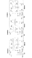
図1を参照すると、本発明に係る複合バランは、複数個のバランBL1〜BL3と、少なくとも1つのキャパシタC11〜C13と、直流電圧供給端子T20とを含む。バランBL1〜BL3は、図示では3個であるが、2個以上あればよい。キャパシタC11〜C13は、基本的には、バランBL1〜BL3の個数に対応する。 Referring to FIG. 1, the composite balun according to the present invention includes a plurality of baluns BL1 to BL3, at least one capacitor C11 to C13, and a DC voltage supply terminal T20. Although the number of baluns BL1 to BL3 is three in the drawing, two or more baluns are sufficient. The capacitors C11 to C13 basically correspond to the number of baluns BL1 to BL3.
バランBL1〜BL3及びキャパシタC11〜C13は、1つのチップ1内に内蔵されている。このようなチップ1は、通常は、6面体状のセラミック誘電体で構成され、その内部に必要な導体パターンを層状に埋設し、層間に配置された貫通電極によって、導体パターンを導通させることによって得られる。
The baluns BL1 to BL3 and the capacitors C11 to C13 are built in one
バランBL1〜BL3のそれぞれは、第1乃至第4結合線路(L11〜L14)〜(L31〜L34)と、第1平衡端子(T2、T5、T8)と、第2平衡端子(T1、T6、T9)と、不平衡端子(T15、T18、T12)とを含んでいる。 Each of the baluns BL1 to BL3 includes first to fourth coupled lines (L11 to L14) to (L31 to L34), a first balanced terminal (T2, T5, T8), and a second balanced terminal (T1, T6, T9) and unbalanced terminals (T15, T18, T12).
バランBL1〜BL3は、基本的な構成が互いに一致している。もっとも、共振周波数は互いに異なるので、結合線路のパターン及び長さなどは異なる。バランBL1〜BL3について、個別的に説明すると次のとおりである。まず、バランBL1において、第1結合線路L11は、一端が不平衡端子T18に接続されており、第2結合線路L12は、一端が第1結合線路L11の他端に接続されている。第3結合線路L13は、第1結合線路L11に電磁結合し、一端が第1平衡端子T2に接続され、他端が直流電圧供給端子T20に接続されており、第4結合線路L14は、第2結合線路L12に電磁結合し、一端が第2平衡端子T1に接続され、他端が直流電圧供給端子T20に接続されている。第1乃至第4結合線路L11〜L14は、対象とする周波数信号の波長λに対して、λ/4の線路長を有するストリップラインとして構成される。第1結合線路L11と第3結合線路L13は、セラミック誘電体層を間に挟んで互いに対向し、それによって、電磁結合を生じさせる。第2結合線路L12と第4結合線路L14も同様であって、セラミック誘電体層を間に挟んで互いに対向し、それによって、電磁結合を生じさせる。 The basic configurations of the baluns BL1 to BL3 are the same. However, since the resonance frequencies are different from each other, the pattern and length of the coupled line are different. The baluns BL1 to BL3 are individually described as follows. First, in the balun BL1, one end of the first coupling line L11 is connected to the unbalanced terminal T18, and one end of the second coupling line L12 is connected to the other end of the first coupling line L11. The third coupled line L13 is electromagnetically coupled to the first coupled line L11, one end is connected to the first balanced terminal T2, the other end is connected to the DC voltage supply terminal T20, and the fourth coupled line L14 is The two coupled lines L12 are electromagnetically coupled, one end is connected to the second balanced terminal T1, and the other end is connected to the DC voltage supply terminal T20. The first to fourth coupled lines L11 to L14 are configured as strip lines having a line length of λ / 4 with respect to the wavelength λ of the target frequency signal. The first coupling line L11 and the third coupling line L13 are opposed to each other with the ceramic dielectric layer in between, thereby causing electromagnetic coupling. The second coupling line L12 and the fourth coupling line L14 are the same, and are opposed to each other with the ceramic dielectric layer interposed therebetween, thereby causing electromagnetic coupling.
キャパシタC11は、一端が、直流電圧供給端子T20に接続され、他端が接地端子に導かれている。キャパシタC11は、チップを構成するセラミック誘電体層を挟んで互いに対向する少なくとも一対の電極を含んでおり、セラミック誘電体層の誘電率、厚み、及び電極面積によって定まる。 One end of the capacitor C11 is connected to the DC voltage supply terminal T20, and the other end is led to the ground terminal. The capacitor C11 includes at least a pair of electrodes facing each other with the ceramic dielectric layer constituting the chip interposed therebetween, and is determined by the dielectric constant, thickness, and electrode area of the ceramic dielectric layer.
次に、バランBL2において、第1結合線路L21は、一端が不平衡端子T15に接続されており、第2結合線路L22は、一端が第1結合線路L21の他端に接続されている。第3結合線路L23は、第1結合線路L21に電磁結合し、一端が第1平衡端子T5に接続され、他端が直流電圧供給端子T20に接続されている。第4結合線路L24は、第2結合線路L22に電磁結合し、一端が第2平衡端子T6に接続され、他端が直流電圧供給端子T20に接続されている。第1乃至第4結合線路L21〜L24も、対象とする周波数信号の波長λに対して、λ/4の線路長を有するストリップラインとして構成される。第1結合線路L21と第3結合線路L23は、誘電体層を間に挟んで互いに対向し、それによって、電磁結合を生じさせる。第2結合線路L22と第4結合線路L24も同様であって、誘電体層を間に挟んで互いに対向し、それによって、電磁結合を生じさせる。 Next, in the balun BL2, one end of the first coupling line L21 is connected to the unbalanced terminal T15, and one end of the second coupling line L22 is connected to the other end of the first coupling line L21. The third coupled line L23 is electromagnetically coupled to the first coupled line L21, one end is connected to the first balanced terminal T5, and the other end is connected to the DC voltage supply terminal T20. The fourth coupled line L24 is electromagnetically coupled to the second coupled line L22, one end is connected to the second balanced terminal T6, and the other end is connected to the DC voltage supply terminal T20. The first to fourth coupled lines L21 to L24 are also configured as strip lines having a line length of λ / 4 with respect to the wavelength λ of the target frequency signal. The first coupling line L21 and the third coupling line L23 are opposed to each other with the dielectric layer interposed therebetween, thereby causing electromagnetic coupling. The same applies to the second coupling line L22 and the fourth coupling line L24, which face each other with the dielectric layer in between, thereby causing electromagnetic coupling.
キャパシタC12は、一端が、直流電圧供給端子T20に接続され、他端が接地端子に導かれている。キャパシタC12は、チップを構成するセラミック誘電体層を挟んで互いに対向する少なくとも一対の電極を含んでおり、セラミック誘電体層の誘電率、厚み、及び電極面積によって定まる。 One end of the capacitor C12 is connected to the DC voltage supply terminal T20, and the other end is led to the ground terminal. The capacitor C12 includes at least a pair of electrodes facing each other with the ceramic dielectric layer constituting the chip interposed therebetween, and is determined by the dielectric constant, thickness, and electrode area of the ceramic dielectric layer.
更に、バランBL3において、第1結合線路L31は、一端が不平衡端子T12に接続されており、第2結合線路L32は、一端が第1結合線路L31の他端に接続されている。第3結合線路L33は、第1結合線路L31に電磁結合し、一端が第1平衡端子T8に接続され、他端が直流電圧供給端子T20に接続されており、第4結合線路L34は、第2結合線路L32に電磁結合し、一端が第2平衡端子T9に接続され、他端が直流電圧供給端子T20に接続されている。第1乃至第4結合線路L31〜L34は、対象とする周波数信号の波長λに対して、λ/4の線路長を有するストリップラインとして構成される。第1結合線路L31と第3結合線路L33は、セラミック誘電体層を間に挟んで互いに対向し、それによって、電磁結合を生じさせる。第2結合線路L32と第4結合線路L34も同様であって、セラミック誘電体層を間に挟んで互いに対向し、それによって、電磁結合を生じさせる。 Further, in the balun BL3, one end of the first coupling line L31 is connected to the unbalanced terminal T12, and one end of the second coupling line L32 is connected to the other end of the first coupling line L31. The third coupled line L33 is electromagnetically coupled to the first coupled line L31, one end is connected to the first balanced terminal T8, the other end is connected to the DC voltage supply terminal T20, and the fourth coupled line L34 is The two coupled lines L32 are electromagnetically coupled, one end is connected to the second balanced terminal T9, and the other end is connected to the DC voltage supply terminal T20. The first to fourth coupled lines L31 to L34 are configured as strip lines having a line length of λ / 4 with respect to the wavelength λ of the target frequency signal. The first coupling line L31 and the third coupling line L33 are opposed to each other with the ceramic dielectric layer interposed therebetween, thereby causing electromagnetic coupling. The second coupling line L32 and the fourth coupling line L34 are the same, and are opposed to each other with the ceramic dielectric layer interposed therebetween, thereby generating electromagnetic coupling.
キャパシタC13は、一端が、直流電圧供給端子T20に接続され、他端が接地端子に導かれている。キャパシタC13は、チップを構成するセラミック誘電体層を挟んで互いに対向する少なくとも一対の電極を含んでおり、セラミック誘電体層の誘電率、厚み、及び電極面積によって定まる。 One end of the capacitor C13 is connected to the DC voltage supply terminal T20, and the other end is led to the ground terminal. The capacitor C13 includes at least a pair of electrodes facing each other across the ceramic dielectric layer constituting the chip, and is determined by the dielectric constant, thickness, and electrode area of the ceramic dielectric layer.
上述したように、本発明に係る複合バランは、その主要部である複数個のバランBL1〜BL3は、1つのチップ1内に内蔵されているから、複数のバランBL1〜BL3を携帯電話などの移動体通信機、無線LANなどに組み込む場合には、1個分の実装面積をプリント基板上に確保すればよく、小型化の要請に応えることができる。
As described above, in the composite balun according to the present invention, the plurality of baluns BL1 to BL3, which are the main parts, are built in one
複数のバランBL1〜BL3のそれぞれにおいて、第1結合線路(L11、L21、L31)は、一端が不平衡端子(T18、T15、T12)に接続されており、第2結合線路(L12、L22、L32)は、一端が第1結合線路(L11、L21、L31)の他端に接続されており、第3結合線路(L13、L23、L33)は、第1結合線路(L11、L21、L31)に電磁結合され、一端が第1平衡端子(T2、T5、T8)に接続され、第4結合線路(L14、L24、L34)は、第2結合線路(L12、L22、L32)に電磁結合され、一端が第2平衡端子(T1、T6、T9)に接続されているから、第3及び第4結合線路(L13、L23、L33)、(L14、L24、L34)を平衡伝送線路とし、第1及び第2結合線路(L11、L21、L31)、(L12、L22、L32)を不平衡伝送線路とする複合バランが得られる。 In each of the plurality of baluns BL1 to BL3, one end of the first coupled line (L11, L21, L31) is connected to the unbalanced terminal (T18, T15, T12), and the second coupled line (L12, L22, L32) has one end connected to the other end of the first coupled line (L11, L21, L31), and the third coupled line (L13, L23, L33) is the first coupled line (L11, L21, L31). Are coupled to the first balanced terminals (T2, T5, T8), and the fourth coupled lines (L14, L24, L34) are electromagnetically coupled to the second coupled lines (L12, L22, L32). Since one end is connected to the second balanced terminal (T1, T6, T9), the third and fourth coupled lines (L13, L23, L33), (L14, L24, L34) are used as balanced transmission lines. 1 and 2 If line (L11, L21, L31), the composite balun is obtained and (L12, L22, L32) the unbalanced transmission line.
第3結合線路(L13、L23、L33)は、他端が直流電圧供給端子T20に接続されており、第4結合線路(L14、L24、L34)は、他端が直流電圧供給端子T20に接続されているから、電力増幅器や、無線周波数集積回路に直流電圧を供給する必要がある場合に、複合バランを通して直流電圧を供給しえる使い勝手のよい複合バランが得られる。 The other end of the third coupled line (L13, L23, L33) is connected to the DC voltage supply terminal T20, and the other end of the fourth coupled line (L14, L24, L34) is connected to the DC voltage supply terminal T20. Therefore, when it is necessary to supply a DC voltage to a power amplifier or a radio frequency integrated circuit, an easy-to-use composite balun that can supply a DC voltage through the composite balun can be obtained.
更に、一端が直流電圧供給端子T20に接続され、他端が接地端子に導かれているキャパシタC11〜C13を含んでいるから、電源供給回路を経由して侵入するノイズをキャパシタC11〜C13によって吸収し得る。しかも、このキャパシタC11〜C13は、複数個のバランBL1〜BL3と共に、1つのチップ1内に内蔵されているから、複合バランにキャパシタC11〜C13を外付けする場合と対比して、ユーザ側の実装作業が容易になるとともに、回路基板上で見た実装面積が縮小される。
Furthermore, since it includes capacitors C11 to C13 having one end connected to the DC voltage supply terminal T20 and the other end led to the ground terminal, noise entering through the power supply circuit is absorbed by the capacitors C11 to C13. Can do. In addition, since the capacitors C11 to C13 are built in one
次に、図2を参照して、本発明に係る複合バランの他の実施の形態を説明する。図2において、図1に現れた構成部分と同一性のある構成部分については、同一の参照符号を付し、重複説明は、これを省略する。この実施の形態の特徴は、キャパシタC1が、複数のバランBL1〜BL3において、共用されていることである。即ち、バランBL1〜BL3は複数であるが、キャパシタC1は、回路上、一個だけである。複数個のキャパシタを並列接続、または、直列接続する場合でも、電気回路上、等価的に一個のキャパシタとして表現される場合は、ここにいう一個のキャパシタである。 Next, another embodiment of the composite balun according to the present invention will be described with reference to FIG. In FIG. 2, the same reference numerals are given to the components that are the same as the components that appear in FIG. 1, and duplicate descriptions are omitted. A feature of this embodiment is that the capacitor C1 is shared by the plurality of baluns BL1 to BL3. That is, the baluns BL1 to BL3 are plural, but the capacitor C1 is only one on the circuit. Even when a plurality of capacitors are connected in parallel or in series, if they are equivalently expressed as one capacitor on the electric circuit, this is one capacitor.
上記構成であれば、複数個のバランBL1〜BL3を備えながら、キャパシタC1は一個で済むので、小型化をより進展させることができる。また、実際に製品化する場合の積層構造を単純化し、小型化及びコストダウンに資することができる。 If it is the said structure, since the capacitor C1 may be sufficient while providing several baluns BL1-BL3, size reduction can be advanced further. In addition, it is possible to simplify the laminated structure in the case of actual production, contributing to downsizing and cost reduction.
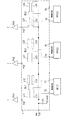
次に、図3を参照して、図2に示した複合バランの使用した一例を説明する。図1に示した複合バランも同様の状態で用いることができる。バランBL1〜BL3の不平衡端子T18、T15及びT12のそれぞれには、電力増幅器PA1〜PA3が接続されており、対の平衡端子(T2、T1)、(T5、T6)及び(T8、T9)のそれぞれには、無線周波数集積回路RFIC1〜RFIC4が接続されている。バランBL1〜BL3のそれぞれは、平衡信号を扱う無線周波数集積回路RFIC1〜RFIC4と、不平衡信号を扱う電力増幅器PA1〜PA3との間に介在し、平衡−不平衡変換器として動作する。 Next, an example in which the composite balun shown in FIG. 2 is used will be described with reference to FIG. The composite balun shown in FIG. 1 can be used in the same state. The power amplifiers PA1 to PA3 are connected to the unbalanced terminals T18, T15, and T12 of the baluns BL1 to BL3, respectively, and a pair of balanced terminals (T2, T1), (T5, T6), and (T8, T9). Each of these is connected to radio frequency integrated circuits RFIC1 to RFIC4. Each of the baluns BL1 to BL3 is interposed between the radio frequency integrated circuits RFIC1 to RFIC4 that handle balanced signals and the power amplifiers PA1 to PA3 that handle unbalanced signals, and operate as a balanced-unbalanced converter.
この場合、既に述べたように、本発明に係る複合バランでは、第3結合線路(L13、L23、L33)は、他端が直流電圧供給端子T20に接続されており、第4結合線路(L14、L24、L34)は、他端が直流電圧供給端子T20に接続されているから、直流電圧を供給する必要のある電力増幅器PA1〜PA3及び無線周波数集積回路RFIC1〜RFIC4に対し、複合バランを通して直流電圧Vccを供給しえる。 In this case, as already described, in the composite balun according to the present invention, the other end of the third coupled line (L13, L23, L33) is connected to the DC voltage supply terminal T20, and the fourth coupled line (L14 , L24, and L34) are connected to the DC voltage supply terminal T20 at the other end, so that the power amplifiers PA1 to PA3 and the radio frequency integrated circuits RFIC1 to RFIC4 that need to supply a DC voltage are DC-connected through a composite balun. The voltage Vcc can be supplied.
更に、一端が直流電圧供給端子T20に接続され、他端が接地端子GROUNDに導かれているキャパシタC1を含んでいるから、電源供給回路を経由して侵入するノイズをキャパシタC1によって吸収し得る。しかも、このキャパシタC1は、複数個のバランBL1〜BL3と共に、1つのチップ1内に内蔵されているから、複合バランにキャパシタC1を外付けする場合と対比して、ユーザ側の実装作業が容易になるとともに、回路基板上で見た実装面積が縮小される。
Furthermore, since the capacitor C1 having one end connected to the DC voltage supply terminal T20 and the other end led to the ground terminal GROUND is included, noise entering through the power supply circuit can be absorbed by the capacitor C1. In addition, since the capacitor C1 is built in one
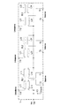
次に、図2に図示した複合バランについて、図4〜図7を参照し、その具体的な積層構造を説明する。まず、図4を参照すると、誘電体層LY1〜LY18を順次に積層した構造が記載されている。誘電体層LY1〜LY18は、何れも、セラミック誘電体シートを積層した後焼成して一体化されたもので、実際には図示の分解された状態にはない。図4は、単に構造を説明するために各層に分解して示したものである。 Next, a specific laminated structure of the composite balun illustrated in FIG. 2 will be described with reference to FIGS. First, referring to FIG. 4, a structure in which dielectric layers LY1 to LY18 are sequentially stacked is described. The dielectric layers LY1 to LY18 are integrated by firing after laminating ceramic dielectric sheets, and are not actually in the disassembled state shown in the figure. FIG. 4 is an exploded view of each layer simply to explain the structure.
まず、最下層の誘電体層LY1は、図4にも拡大して示すように、下面の周辺部に端子T1〜T20が所定の間隔を隔てて配置されている。端子T1〜T20は、誘電体層LY1の下面に限って形成してあるので、複合バランを基板に実装する場合、接続用半田のフィレットが形成されることがない。このため、実装面積が縮小される。端子T1〜T20のうち、端子T1はバランBL1の第2平衡端子、端子T2は同じく第1平衡端子、端子T5、T6はバランBL2の第1及び第2平衡端子、端子T8、T9はバランBL3の第1及び第2平衡端子を、それぞれ構成する。また、端子T18はバランBL1の不平衡端子、端子15はバランBL2の不平衡端子、端子12はバランBL3の不平衡端子である。残りの端子T3、T4、T7、T10、T11、T13、T14、T16、T17及びT19は、接地端子として用いられる。端子T20は直流電圧供給端子である。 First, as shown in FIG. 4 in an enlarged manner, the lowermost dielectric layer LY1 has terminals T1 to T20 arranged at predetermined intervals on the periphery of the lower surface. Since the terminals T1 to T20 are formed only on the lower surface of the dielectric layer LY1, when the composite balun is mounted on the substrate, a connection solder fillet is not formed. For this reason, the mounting area is reduced. Among the terminals T1 to T20, the terminal T1 is the second balanced terminal of the balun BL1, the terminal T2 is also the first balanced terminal, the terminals T5 and T6 are the first and second balanced terminals of the balun BL2, and the terminals T8 and T9 are the balun BL3. The first and second balanced terminals are respectively configured. The terminal T18 is an unbalanced terminal of the balun BL1, the terminal 15 is an unbalanced terminal of the balun BL2, and the terminal 12 is an unbalanced terminal of the balun BL3. The remaining terminals T3, T4, T7, T10, T11, T13, T14, T16, T17 and T19 are used as ground terminals. Terminal T20 is a DC voltage supply terminal.
次に、誘電体層LY1の上に順次に重なる誘電体層LY2、LY3及びLY4は、図2に示したキャパシタC1を構成する。キャパシタC1は、図6にも拡大して示すように、中間部の誘電体層LY3の表面に形成された電極E1と、その下に位置する誘電体層LY2の表面に形成された接地電極G1との間に生じるキャパシタC01、及び、誘電体層LY3の電極E1とその上に位置する誘電体層LY4の表面に形成された接地電極G2との間に生じるキャパシタC02を並列接続した構造となる。従って、キャパシタC1のキャパシタンスC1は、C1=C01+C02となる。 Next, the dielectric layers LY2, LY3, and LY4 that sequentially overlap the dielectric layer LY1 constitute the capacitor C1 shown in FIG. As shown in FIG. 6 in an enlarged manner, the capacitor C1 includes an electrode E1 formed on the surface of the intermediate dielectric layer LY3 and a ground electrode G1 formed on the surface of the dielectric layer LY2 positioned therebelow. And a capacitor C02 generated between the electrode E1 of the dielectric layer LY3 and the ground electrode G2 formed on the surface of the dielectric layer LY4 positioned thereon are connected in parallel. . Accordingly, the capacitance C1 of the capacitor C1 is C1 = C01 + C02.
誘電体層LY4の上に位置する誘電体層LY5は、貫通電極Hの群を設けたスペーサ層であり、その上に、配線パターン群P1を有する誘電体層LY6及び配線パターン群P2を有する誘電体層LY7が順次に重なる。 The dielectric layer LY5 located on the dielectric layer LY4 is a spacer layer provided with a group of through electrodes H, and a dielectric layer LY6 having a wiring pattern group P1 and a dielectric layer having a wiring pattern group P2 thereon. The body layers LY7 are sequentially overlapped.
誘電体層LY7の上に順次に重なる誘電体層LY8〜LY15は、バランBL1〜BL3の第1結合線路〜第4結合線路を構成するために用いられる。その詳細は、図7に図示されている。図7を参照するに、まず、誘電体層LY8の一面上には、バランBL1の第4結合線路L14を構成するストリップ状導体及び同じく第3結合線路L13を構成するストリップ状導体が、間隔を隔てて一方向に横並びに配置されている。第3結合線路L13の横方向には、間隔をへだてて、バランBL2の第3結合線路L23を構成するストリップ状導体及び同じく第4結合線路L24を構成するストリップ状導体が、互いに間隔を隔てて一方向に横並びに配置されている。更に、バランBL2の第4結合線路L24の横方向には、間隔をへだてて、バランBL3の第3結合線路L33を構成するストリップ状導体及び同じく第4結合線路L34を構成するストリップ状導体が、互いに間隔を隔てて一方向に横並びに配置されている。 The dielectric layers LY8 to LY15 sequentially overlapping the dielectric layer LY7 are used to configure the first to fourth coupled lines of the baluns BL1 to BL3. The details are shown in FIG. Referring to FIG. 7, first, on one surface of the dielectric layer LY8, a strip-shaped conductor constituting the fourth coupled line L14 of the balun BL1 and a strip-shaped conductor constituting the third coupled line L13 are spaced apart. They are arranged side by side in one direction. In the lateral direction of the third coupled line L13, the strip-shaped conductors constituting the third coupled line L23 of the balun BL2 and the strip-shaped conductors also constituting the fourth coupled line L24 are spaced apart from each other at an interval. They are arranged side by side in one direction. Further, in the lateral direction of the fourth coupling line L24 of the balun BL2, the strip-shaped conductors constituting the third coupling line L33 of the balun BL3 and the strip-like conductors constituting the fourth coupling line L34 are spaced apart from each other. They are arranged side by side in one direction at intervals.
次に、誘電体層LY8の上に重なる誘電体層LY9の一面上には、バランBL1の第2結合線路L12を構成するストリップ状導体及び同じく第1結合線路L11を構成するストリップ状導体が、間隔を隔てて一方向に横並びに配置されている。第1結合線路L11の横方向には、間隔をへだてて、バランBL2の第1結合線路L21を構成するストリップ状導体及び同じく第2結合線路L22を構成するストリップ状導体が、互いに間隔を隔てて一方向に横並びに配置されている。更に、バランBL2の第2結合線路L22の横方向には、間隔をへだてて、バランBL3の第1結合線路L31を構成するストリップ状導体及び同じく第2結合線路L32を構成するストリップ状導体が、互いに間隔を隔てて一方向に横並びに配置されている。 Next, on one surface of the dielectric layer LY9 overlying the dielectric layer LY8, a strip-like conductor constituting the second coupling line L12 of the balun BL1 and a strip-like conductor similarly constituting the first coupling line L11 are provided. They are arranged side by side in one direction at intervals. In the lateral direction of the first coupling line L11, the strip-like conductors constituting the first coupling line L21 of the balun BL2 and the strip-like conductors constituting the second coupling line L22 are spaced apart from each other with a gap therebetween. They are arranged side by side in one direction. Further, in the lateral direction of the second coupling line L22 of the balun BL2, a strip-shaped conductor constituting the first coupling line L31 of the balun BL3 and a strip-like conductor also constituting the second coupling line L32 are spaced apart from each other. They are arranged side by side in one direction at intervals.
従って、誘電体層LY8と誘電体層LY9との間では、バランBL1に関して、第1結合線路L11と第3結合線路L13、及び、第2結合線路L12と第4結合線路L14が、誘電体層LY9を介して、電磁結合することになる。バランBL2に関しては、第1結合線路L21と第3結合線路L23、及び、第2結合線路L22と第4結合線路L24が、誘電体層LY9を介して、電磁結合する。更に、バランBL3に関しては、第1結合線路L31と第3結合線路L33、及び、第2結合線路L32と第4結合線路L34が、誘電体層LY9を介して、電磁結合する。 Therefore, between the dielectric layer LY8 and the dielectric layer LY9, with respect to the balun BL1, the first coupled line L11 and the third coupled line L13, and the second coupled line L12 and the fourth coupled line L14 are dielectric layers. Electromagnetic coupling is performed via LY9. Regarding the balun BL2, the first coupled line L21 and the third coupled line L23, and the second coupled line L22 and the fourth coupled line L24 are electromagnetically coupled through the dielectric layer LY9. Further, regarding the balun BL3, the first coupling line L31 and the third coupling line L33, and the second coupling line L32 and the fourth coupling line L34 are electromagnetically coupled via the dielectric layer LY9.
次に、誘電体層LY9の上に重なる誘電体層LY10の一面上には、バランBL1の第4結合線路L14を構成するストリップ状導体、及び、同じく第3結合線路L13を構成するストリップ状導体が、間隔を隔てて一方向に横並びに配置されている。第3結合線路L13の横方向には、間隔をへだてて、バランBL2の第3結合線路L23を構成するストリップ状導体、及び、同じく第4結合線路L24を構成するストリップ状導体が、互いに間隔を隔てて一方向に横並びに配置されている。更に、バランBL2の第4結合線路L24の横方向には、間隔をへだてて、バランBL3の第3結合線路L33を構成するストリップ状導体、及び、同じく第4結合線路L34を構成するストリップ状導体が、互いに間隔を隔てて一方向に横並びに配置されている。 Next, on one surface of the dielectric layer LY10 overlying the dielectric layer LY9, a strip-like conductor constituting the fourth coupling line L14 of the balun BL1, and a strip-like conductor also constituting the third coupling line L13 are provided. Are arranged side by side in one direction at intervals. In the lateral direction of the third coupled line L13, the strip-shaped conductors constituting the third coupled line L23 of the balun BL2 and the strip-shaped conductors also constituting the fourth coupled line L24 are spaced apart from each other at an interval. They are arranged side by side in one direction. Further, in the lateral direction of the fourth coupling line L24 of the balun BL2, a strip-like conductor constituting the third coupling line L33 of the balun BL3 and a strip-like conductor also constituting the fourth coupling line L34 are spaced apart from each other. Are arranged side by side in one direction at intervals.
従って、誘電体層LY9と誘電体層LY10との間では、バランBL1に関しては、第1結合線路L11と第3結合線路L13、及び、第2結合線路L12と第4結合線路L14が、誘電体層LY10を介して、電磁結合することになる。バランBL2に関しては、第1結合線路L21と第3結合線路L23、及び、第2結合線路L22と第4結合線路L24が、誘電体層LY10を介して、電磁結合する。更に、バランBL3に関しては、第1結合線路L31と第3結合線路L33、及び、第2結合線路L32と第4結合線路L34が、誘電体層LY10を介して、電磁結合する。 Therefore, between the dielectric layer LY9 and the dielectric layer LY10, with respect to the balun BL1, the first coupling line L11 and the third coupling line L13, and the second coupling line L12 and the fourth coupling line L14 are dielectrics. Electromagnetic coupling will occur through the layer LY10. Regarding the balun BL2, the first coupling line L21 and the third coupling line L23, and the second coupling line L22 and the fourth coupling line L24 are electromagnetically coupled via the dielectric layer LY10. Further, regarding the balun BL3, the first coupling line L31 and the third coupling line L33, and the second coupling line L32 and the fourth coupling line L34 are electromagnetically coupled through the dielectric layer LY10.
次に、誘電体層LY10の上に重なる誘電体層LY11の一面上には、バランBL1の第2結合線路L12を構成するストリップ状導体、及び、同じく第1結合線路L11を構成するストリップ状導体が、間隔を隔てて一方向に横並びに配置されている。第1結合線路L11の横方向には、間隔をへだてて、バランBL2の第1結合線路L21を構成するストリップ状導体、及び、同じく第2結合線路L22を構成するストリップ状導体が、互いに間隔を隔てて一方向に横並びに配置されている。更に、バランBL2の第2結合線路L22の横方向には、間隔をへだてて、バランBL3の第1結合線路L31を構成するストリップ状導体及び同じく第2結合線路L32を構成するストリップ状導体が、互いに間隔を隔てて一方向に横並びに配置されている。 Next, on one surface of the dielectric layer LY11 that overlaps the dielectric layer LY10, a strip-shaped conductor that constitutes the second coupling line L12 of the balun BL1, and a strip-like conductor that also constitutes the first coupling line L11. Are arranged side by side in one direction at intervals. In the lateral direction of the first coupled line L11, the strip-shaped conductors constituting the first coupled line L21 of the balun BL2 and the strip-shaped conductors also constituting the second coupled line L22 are spaced apart from each other at an interval. They are arranged side by side in one direction. Further, in the lateral direction of the second coupling line L22 of the balun BL2, a strip-shaped conductor constituting the first coupling line L31 of the balun BL3 and a strip-like conductor also constituting the second coupling line L32 are spaced apart from each other. They are arranged side by side in one direction at intervals.
従って、誘電体層LY10と誘電体層LY11との間では、バランBL1に関しては、第1結合線路L11と第3結合線路L13、及び、第2結合線路L12と第4結合線路L14が、誘電体層LY11を介して、電磁結合することになる。バランBL2に関しては、第1結合線路L21と第3結合線路L23、及び、第2結合線路L22と第4結合線路L24が、誘電体層LY11を介して、電磁結合する。更に、バランBL3に関しては、第1結合線路L31と第3結合線路L33、及び、第2結合線路L32と第4結合線路L34が、誘電体層LY11を介して、電磁結合する。 Therefore, between the dielectric layer LY10 and the dielectric layer LY11, with respect to the balun BL1, the first coupling line L11 and the third coupling line L13, and the second coupling line L12 and the fourth coupling line L14 are dielectrics. Electromagnetic coupling will occur via the layer LY11. Regarding the balun BL2, the first coupling line L21 and the third coupling line L23, and the second coupling line L22 and the fourth coupling line L24 are electromagnetically coupled via the dielectric layer LY11. Further, regarding the balun BL3, the first coupling line L31 and the third coupling line L33, and the second coupling line L32 and the fourth coupling line L34 are electromagnetically coupled via the dielectric layer LY11.
更に、誘電体層LY11の上に重なる誘電体層LY12の一面上には、バランBL1の第4結合線路L14を構成するストリップ状導体、及び、同じく第3結合線路L13を構成するストリップ状導体が、間隔を隔てて一方向に横並びに配置されている。第3結合線路L13の横方向には、間隔をへだてて、バランBL2の第3結合線路L23を構成するストリップ状導体、及び、同じく第4結合線路L24を構成するストリップ状導体が、互いに間隔を隔てて一方向に横並びに配置されている。更に、バランBL2の第4結合線路L24の横方向には、間隔をへだてて、バランBL3の第3結合線路L33を構成するストリップ状導体、及び、同じく第4結合線路L34を構成するストリップ状導体が、互いに間隔を隔てて一方向に横並びに配置されている。 Further, on one surface of the dielectric layer LY12 overlapping the dielectric layer LY11, a strip-shaped conductor constituting the fourth coupled line L14 of the balun BL1 and a strip-shaped conductor also constituting the third coupled line L13 are provided. Are arranged side by side in one direction at intervals. In the lateral direction of the third coupled line L13, the strip-shaped conductors constituting the third coupled line L23 of the balun BL2 and the strip-shaped conductors also constituting the fourth coupled line L24 are spaced apart from each other at an interval. They are arranged side by side in one direction. Further, in the lateral direction of the fourth coupling line L24 of the balun BL2, a strip-like conductor constituting the third coupling line L33 of the balun BL3 and a strip-like conductor also constituting the fourth coupling line L34 are spaced apart from each other. Are arranged side by side in one direction at intervals.
従って、誘電体層LY11と誘電体層LY12との間では、バランBL1に関しては、第1結合線路L11と第3結合線路L13、及び、第2結合線路L12と第4結合線路L14が、誘電体層LY12を介して、電磁結合することになる。バランBL2に関しては、第1結合線路L21と第3結合線路L23、及び、第2結合線路L22と第4結合線路L24が、誘電体層LY12を介して、電磁結合する。更に、バランBL3に関しては、第1結合線路L31と第3結合線路L33、及び、第2結合線路L32と第4結合線路L34が、誘電体層LY12を介して、電磁結合する。 Therefore, between the dielectric layer LY11 and the dielectric layer LY12, with respect to the balun BL1, the first coupling line L11 and the third coupling line L13, and the second coupling line L12 and the fourth coupling line L14 are dielectrics. Electromagnetic coupling will occur through the layer LY12. Regarding the balun BL2, the first coupled line L21 and the third coupled line L23, and the second coupled line L22 and the fourth coupled line L24 are electromagnetically coupled via the dielectric layer LY12. Further, regarding the balun BL3, the first coupling line L31 and the third coupling line L33, and the second coupling line L32 and the fourth coupling line L34 are electromagnetically coupled via the dielectric layer LY12.
誘電体層LY12の上に重なる誘電体層LY13の一面上には、バランBL1の第2結合線路L12を構成するストリップ状導体、及び、同じく第1結合線路L11を構成するストリップ状導体が、間隔を隔てて一方向に横並びに配置されている。第1結合線路L11の横方向には、間隔をへだてて、バランBL2の第1結合線路L21を構成するストリップ状導体、及び、同じく第2結合線路L22を構成するストリップ状導体が、互いに間隔を隔てて一方向に横並びに配置されている。更に、バランBL2の第2結合線路L22の横方向には、間隔をへだてて、バランBL3の第1結合線路L31を構成するストリップ状導体及び同じく第2結合線路L32を構成するストリップ状導体が、互いに間隔を隔てて一方向に横並びに配置されている。 On one surface of the dielectric layer LY13 that overlaps with the dielectric layer LY12, a strip-shaped conductor that constitutes the second coupling line L12 of the balun BL1 and a strip-shaped conductor that also constitutes the first coupling line L11 are spaced apart. They are arranged side by side in one direction with a gap therebetween. In the lateral direction of the first coupled line L11, the strip-shaped conductors constituting the first coupled line L21 of the balun BL2 and the strip-shaped conductors also constituting the second coupled line L22 are spaced apart from each other at an interval. They are arranged side by side in one direction. Further, in the lateral direction of the second coupling line L22 of the balun BL2, a strip-shaped conductor constituting the first coupling line L31 of the balun BL3 and a strip-like conductor also constituting the second coupling line L32 are spaced apart from each other. They are arranged side by side in one direction at intervals.
従って、誘電体層LY12と誘電体層LY13との間では、バランBL1に関しては、第1結合線路L11と第3結合線路L13、及び、第2結合線路L12と第4結合線路L14が、誘電体層LY13を介して、電磁結合することになる。バランBL2に関しては、第1結合線路L21と第3結合線路L23、及び、第2結合線路L22と第4結合線路L24が、誘電体層LY13を介して、電磁結合する。更に、バランBL3に関しては、第1結合線路L31と第3結合線路L33、及び、第2結合線路L32と第4結合線路L34が、誘電体層LY13を介して、電磁結合する。 Accordingly, between the dielectric layer LY12 and the dielectric layer LY13, with respect to the balun BL1, the first coupling line L11 and the third coupling line L13, and the second coupling line L12 and the fourth coupling line L14 are dielectrics. Electromagnetic coupling will occur through the layer LY13. Regarding the balun BL2, the first coupling line L21 and the third coupling line L23, and the second coupling line L22 and the fourth coupling line L24 are electromagnetically coupled via the dielectric layer LY13. Further, regarding the balun BL3, the first coupling line L31 and the third coupling line L33, and the second coupling line L32 and the fourth coupling line L34 are electromagnetically coupled via the dielectric layer LY13.
誘電体層LY13の上に重なる誘電体層LY14の一面上には、バランBL3の第3結合線路L33を構成するストリップ状導体、及び、同じく第4結合線路L34を構成するストリップ状導体が、互いに間隔を隔てて一方向に横並びに配置されている。 On one surface of the dielectric layer LY14 overlying the dielectric layer LY13, a strip-like conductor constituting the third coupling line L33 of the balun BL3 and a strip-like conductor also constituting the fourth coupling line L34 are mutually connected. They are arranged side by side in one direction at intervals.
従って、誘電体層LY13と誘電体層LY14との間では、バランBL3に関して、第1結合線路L31と第3結合線路L33、及び、第2結合線路L32と第4結合線路L34が、誘電体層LY14を介して、電磁結合する。 Therefore, between the dielectric layer LY13 and the dielectric layer LY14, the first coupling line L31 and the third coupling line L33, and the second coupling line L32 and the fourth coupling line L34 are related to the balun BL3. Electromagnetic coupling is performed via LY14.
誘電体層LY14の上に重なる誘電体層LY15の一面上には、バランBL3の第1結合線路L31を構成するストリップ状導体及び同じく第2結合線路L32を構成するストリップ状導体が、互いに間隔を隔てて一方向に横並びに配置されている。 On one surface of the dielectric layer LY15 overlying the dielectric layer LY14, a strip-like conductor constituting the first coupling line L31 of the balun BL3 and a strip-like conductor constituting the second coupling line L32 are spaced from each other. They are arranged side by side in one direction.
従って、誘電体層LY14と誘電体層LY15との間では、バランBL3に関して、第1結合線路L31と第3結合線路L33、及び、第2結合線路L32と第4結合線路L34が、誘電体層LY15を介して、電磁結合する。 Therefore, between the dielectric layer LY14 and the dielectric layer LY15, the first coupling line L31 and the third coupling line L33, and the second coupling line L32 and the fourth coupling line L34 are related to the balun BL3. Electromagnetic coupling is performed via LY15.
上述したように、第1結合線路(L11、L21、L31)と第3結合線路(L13、L23、L33)との電磁結合、及び、第2結合線路(L12、L22、L32)と第4結合線路(L14、L24、L34)の電磁結合が重層的になっているため、高度で安定な結合度が得られる。しかも、誘電体層1層当たりの結合線路長を短縮し、その平面積を縮小し、小型化を図りながら、必要な線路長を確保することができる。 As described above, the first coupling line (L11, L21, L31) and the third coupling line (L13, L23, L33) are electromagnetically coupled, and the second coupled line (L12, L22, L32) is coupled to the fourth coupling. Since the electromagnetic coupling of the lines (L14, L24, L34) is multi-layered, a high and stable coupling degree can be obtained. In addition, the required line length can be ensured while reducing the coupled line length per dielectric layer, reducing the plane area, and reducing the size.
誘電体層LY8〜LY15に形成されている同一の結合線路は、貫通電極Hにより、図2等で説明された回路構成となるように結線される。例えば、誘電体層LY8に形成された第4結合線路L14、誘電体層LY10に形成された第4結合線路L14、及び、誘電体層LY12に形成された第4結合線路L14は、貫通電極Hによって、基本的には直列接続となるように接続される。第1結合線路(L11、L21、L31)、第2結合線路(L12、L22、L32)及び第3結合線路(L13、L23、L33)、更には、第4結合線路(L24、L34)も、同様の貫通電極Hによる接続処理に付される。 The same coupled line formed in the dielectric layers LY8 to LY15 is connected by the through electrode H so as to have the circuit configuration described in FIG. For example, the fourth coupled line L14 formed on the dielectric layer LY8, the fourth coupled line L14 formed on the dielectric layer LY10, and the fourth coupled line L14 formed on the dielectric layer LY12 are formed of the through electrode H. Are basically connected in series. The first coupled line (L11, L21, L31), the second coupled line (L12, L22, L32), the third coupled line (L13, L23, L33), and the fourth coupled line (L24, L34), A similar connection process using the through electrode H is performed.
図4を参照して、更に説明すると、バランBL1〜BL3を構成する誘電体層LY8〜LY15の下側(図において)には、キャパシタC1の接地電極G1、G2の層があり、しかも、上側には接地電極G3を有する誘電体層LY17がある。即ち、バランBL1〜BL3を、接地電極G1、G2及びG3によってサンドイッチしたシールド構造が得られる。このため、安定したシールド作用が得られる。 With further reference to FIG. 4, the layers of the ground electrodes G1 and G2 of the capacitor C1 are provided on the lower side (in the drawing) of the dielectric layers LY8 to LY15 constituting the baluns BL1 to BL3. Has a dielectric layer LY17 having a ground electrode G3. That is, a shield structure in which the baluns BL1 to BL3 are sandwiched by the ground electrodes G1, G2, and G3 is obtained. For this reason, a stable shielding effect is obtained.
貫通電極Hは、主として、第1結合線路(L11、L21、L31)、第2結合線路(L12、L22、L32)及び第3結合線路(L13、L23、L33)、更には、第4結合線路(L14、L24、L34)を、所定の回路構成となるように接続すること、及び、上下の接地電極G1、G2及びG3を電気的に接続することであるが、バランBL1とバランBL2との間、及び、バランBL2とバランBL3との間に、比較的短い間隔で、接地電極G1、G2またはG3に連なる貫通電極Hの群を形成することにより、バラン間の相互干渉を遮断することができる。 The through electrode H mainly includes a first coupled line (L11, L21, L31), a second coupled line (L12, L22, L32), a third coupled line (L13, L23, L33), and a fourth coupled line. (L14, L24, L34) are connected so as to have a predetermined circuit configuration, and the upper and lower ground electrodes G1, G2, and G3 are electrically connected, but the balun BL1 and the balun BL2 By forming a group of through electrodes H connected to the ground electrodes G1, G2 or G3 at a relatively short interval between the baluns BL2 and BL3, mutual interference between the baluns can be blocked. it can.
以上、好ましい実施例を参照して本発明の内容を具体的に説明したが、本発明の基本的技術思想及び教示に基づいて、当業者であれば、種種の変形態様を採り得ることは自明である。 Although the contents of the present invention have been specifically described above with reference to the preferred embodiments, it is obvious that those skilled in the art can take various modifications based on the basic technical idea and teachings of the present invention. It is.
BL1、BL2、BL3 バラン
L11、L21、L31 第1結合線路
L12、L22、L32 第2結合線路
L13、L23、L33 第3結合線路
L14、L24、L34 第4結合線路
C1、C11、C12、C13 キャパシタ
BL1, BL2, BL3 Baluns L11, L21, L31 First coupled lines L12, L22, L32 Second coupled lines L13, L23, L33 Third coupled lines L14, L24, L34 Fourth coupled lines C1, C11, C12, C13 Capacitors
Claims (2)
前記複数個のバラン及び前記キャパシタは、1つのチップ内に内蔵されており、
前記バランのそれぞれは、第1乃至第4結合線路と、第1平衡端子と、第2平衡端子と、不平衡端子とを含んでおり、
前記第1結合線路は、一端が前記不平衡端子に接続されており、
前記第2結合線路は、一端が前記第1結合線路の他端に接続されており、
前記第3結合線路は、前記第1結合線路に電磁結合し、一端が前記第1平衡端子に接続され、他端が前記直流電圧供給端子に接続されており、
前記第4結合線路は、前記第2結合線路に電磁結合し、一端が前記第2平衡端子に接続され、他端が前記直流電圧供給端子に接続されており、
前記キャパシタは、一端が、前記直流電圧供給端子に接続され、他端が接地端子に導かれており、
前記バランのそれぞれは、前記第1結合線路及び前記第2結合線路と、前記第3結合線路及び前記第4結合線路とが、前記チップを構成する誘電体層を介して電磁結合しており、
前記複数のバランの間では、
前記第1結合線路及び前記第2結合線路を構成するストリップ状導体が、互いに間隔を隔てて一方向に横並びに配置され、
前記第3結合線路及び前記第4結合線路を構成するストリップ状導体が、互いに間隔を隔てて一方向に横並びに配置されており、
前記第1平衡端子、第2平衡端子及び不平衡端子は、最下層の誘電体層の下面の周辺部に、間隔を隔てて配置されており、
前記不平衡端子は、前記最下層の誘電体層の一辺に配置されており、
前記第1平衡端子及び第2平衡端子は、前記最下層の誘電体層の前記一辺と向き合う他の辺に配置されている、
バラン。 A composite balun including a plurality of baluns, at least one capacitor, and a DC voltage supply terminal,
The plurality of baluns and the capacitor are built in one chip,
Each of the baluns includes first to fourth coupled lines, a first balanced terminal, a second balanced terminal, and an unbalanced terminal,
The first coupling line has one end connected to the unbalanced terminal,
One end of the second coupled line is connected to the other end of the first coupled line,
The third coupled line is electromagnetically coupled to the first coupled line, one end is connected to the first balanced terminal, and the other end is connected to the DC voltage supply terminal,
The fourth coupled line is electromagnetically coupled to the second coupled line, one end is connected to the second balanced terminal, and the other end is connected to the DC voltage supply terminal,
The capacitor has one end connected to the DC voltage supply terminal and the other end led to a ground terminal,
In each of the baluns, the first coupling line and the second coupling line, the third coupling line and the fourth coupling line are electromagnetically coupled via a dielectric layer constituting the chip,
Among the plurality of baluns,
Strip-like conductors constituting the first coupling line and the second coupling line are arranged side by side in one direction at intervals from each other,
The strip-like conductors constituting the third coupled line and the fourth coupled line are arranged side by side in one direction at intervals from each other,
The first balanced terminal, the second balanced terminal, and the unbalanced terminal are arranged at intervals in the periphery of the lower surface of the lowermost dielectric layer,
The unbalanced terminal is disposed on one side of the lowermost dielectric layer,
The first balanced terminal and the second balanced terminal are arranged on the other side facing the one side of the lowermost dielectric layer,
Balun.
Priority Applications (2)
| Application Number | Priority Date | Filing Date | Title |
|---|---|---|---|
| JP2009126349A JP4900623B2 (en) | 2009-05-26 | 2009-05-26 | Compound balun |
| US12/774,972 US8324981B2 (en) | 2009-05-26 | 2010-05-06 | Composite balun |
Applications Claiming Priority (1)
| Application Number | Priority Date | Filing Date | Title |
|---|---|---|---|
| JP2009126349A JP4900623B2 (en) | 2009-05-26 | 2009-05-26 | Compound balun |
Publications (2)
| Publication Number | Publication Date |
|---|---|
| JP2010278514A JP2010278514A (en) | 2010-12-09 |
| JP4900623B2 true JP4900623B2 (en) | 2012-03-21 |
Family
ID=43425108
Family Applications (1)
| Application Number | Title | Priority Date | Filing Date |
|---|---|---|---|
| JP2009126349A Active JP4900623B2 (en) | 2009-05-26 | 2009-05-26 | Compound balun |
Country Status (1)
| Country | Link |
|---|---|
| JP (1) | JP4900623B2 (en) |
Family Cites Families (2)
| Publication number | Priority date | Publication date | Assignee | Title |
|---|---|---|---|---|
| JP4783996B2 (en) * | 2001-05-02 | 2011-09-28 | 株式会社村田製作所 | Multi-layer composite balun transformer |
| JP3770883B2 (en) * | 2003-04-17 | 2006-04-26 | 双信電機株式会社 | Passive components |
-
2009
- 2009-05-26 JP JP2009126349A patent/JP4900623B2/en active Active
Also Published As
| Publication number | Publication date |
|---|---|
| JP2010278514A (en) | 2010-12-09 |
Similar Documents
| Publication | Publication Date | Title |
|---|---|---|
| KR100474949B1 (en) | Laminated balun transformer | |
| JP5946024B2 (en) | Directional coupler | |
| WO2015019794A1 (en) | High-frequency module | |
| JP5482901B2 (en) | Directional coupler | |
| TW201644191A (en) | Laminated composite electronic device including coil and capacitor | |
| JP2006094462A (en) | Laminated balun transformer | |
| JPWO2015129597A1 (en) | Multilayer coil element, antenna module, and wireless communication module | |
| JP2009153106A (en) | Band-pass filter, high-frequency component, and communication apparatus | |
| WO2017169102A1 (en) | Electronic component | |
| JP5800113B2 (en) | High frequency module parts | |
| JP2004304615A (en) | High frequency composite part | |
| JP4401981B2 (en) | filter | |
| JP2008182598A (en) | Left-handed system transmission line, bypass filter and communication equipment | |
| KR101983139B1 (en) | Laminated inductor and array of the same | |
| US8324981B2 (en) | Composite balun | |
| JP5218569B2 (en) | Antenna sharing module | |
| JP2003087074A (en) | Laminated filter | |
| JP4900623B2 (en) | Compound balun | |
| JP3153518U (en) | Composite balun | |
| JP2001267141A (en) | Low-pass filter | |
| JP2001185972A (en) | Laminated filter | |
| KR100550843B1 (en) | Miniaturized laminated balance filter | |
| JP5835475B2 (en) | High frequency filter | |
| JP2006262239A (en) | Filter | |
| JP4086154B2 (en) | High frequency composite parts |
Legal Events
| Date | Code | Title | Description |
|---|---|---|---|
| A977 | Report on retrieval |
Free format text: JAPANESE INTERMEDIATE CODE: A971007 Effective date: 20110404 |
|
| A131 | Notification of reasons for refusal |
Free format text: JAPANESE INTERMEDIATE CODE: A131 Effective date: 20110525 |
|
| A521 | Written amendment |
Free format text: JAPANESE INTERMEDIATE CODE: A523 Effective date: 20110721 |
|
| A02 | Decision of refusal |
Free format text: JAPANESE INTERMEDIATE CODE: A02 Effective date: 20110810 |
|
| A521 | Written amendment |
Free format text: JAPANESE INTERMEDIATE CODE: A523 Effective date: 20111107 |
|
| A911 | Transfer of reconsideration by examiner before appeal (zenchi) |
Free format text: JAPANESE INTERMEDIATE CODE: A911 Effective date: 20111114 |
|
| TRDD | Decision of grant or rejection written | ||
| A01 | Written decision to grant a patent or to grant a registration (utility model) |
Free format text: JAPANESE INTERMEDIATE CODE: A01 Effective date: 20111207 |
|
| A01 | Written decision to grant a patent or to grant a registration (utility model) |
Free format text: JAPANESE INTERMEDIATE CODE: A01 |
|
| A61 | First payment of annual fees (during grant procedure) |
Free format text: JAPANESE INTERMEDIATE CODE: A61 Effective date: 20111220 |
|
| R150 | Certificate of patent or registration of utility model |
Ref document number: 4900623 Country of ref document: JP Free format text: JAPANESE INTERMEDIATE CODE: R150 Free format text: JAPANESE INTERMEDIATE CODE: R150 |
|
| FPAY | Renewal fee payment (event date is renewal date of database) |
Free format text: PAYMENT UNTIL: 20150113 Year of fee payment: 3 |