JP4898443B2 - Plasma display panel having a reduced section discharge spreading zone - Google Patents
Plasma display panel having a reduced section discharge spreading zone Download PDFInfo
- Publication number
- JP4898443B2 JP4898443B2 JP2006530445A JP2006530445A JP4898443B2 JP 4898443 B2 JP4898443 B2 JP 4898443B2 JP 2006530445 A JP2006530445 A JP 2006530445A JP 2006530445 A JP2006530445 A JP 2006530445A JP 4898443 B2 JP4898443 B2 JP 4898443B2
- Authority
- JP
- Japan
- Prior art keywords
- cell
- electrodes
- display panel
- coplanar
- discharge
- Prior art date
- Legal status (The legal status is an assumption and is not a legal conclusion. Google has not performed a legal analysis and makes no representation as to the accuracy of the status listed.)
- Expired - Fee Related
Links
Images


Classifications
-
- H—ELECTRICITY
- H01—ELECTRIC ELEMENTS
- H01J—ELECTRIC DISCHARGE TUBES OR DISCHARGE LAMPS
- H01J11/00—Gas-filled discharge tubes with alternating current induction of the discharge, e.g. alternating current plasma display panels [AC-PDP]; Gas-filled discharge tubes without any main electrode inside the vessel; Gas-filled discharge tubes with at least one main electrode outside the vessel
- H01J11/10—AC-PDPs with at least one main electrode being out of contact with the plasma
- H01J11/12—AC-PDPs with at least one main electrode being out of contact with the plasma with main electrodes provided on both sides of the discharge space
-
- H—ELECTRICITY
- H01—ELECTRIC ELEMENTS
- H01J—ELECTRIC DISCHARGE TUBES OR DISCHARGE LAMPS
- H01J11/00—Gas-filled discharge tubes with alternating current induction of the discharge, e.g. alternating current plasma display panels [AC-PDP]; Gas-filled discharge tubes without any main electrode inside the vessel; Gas-filled discharge tubes with at least one main electrode outside the vessel
- H01J11/20—Constructional details
- H01J11/22—Electrodes, e.g. special shape, material or configuration
-
- H—ELECTRICITY
- H01—ELECTRIC ELEMENTS
- H01J—ELECTRIC DISCHARGE TUBES OR DISCHARGE LAMPS
- H01J11/00—Gas-filled discharge tubes with alternating current induction of the discharge, e.g. alternating current plasma display panels [AC-PDP]; Gas-filled discharge tubes without any main electrode inside the vessel; Gas-filled discharge tubes with at least one main electrode outside the vessel
- H01J11/20—Constructional details
- H01J11/34—Vessels, containers or parts thereof, e.g. substrates
- H01J11/36—Spacers, barriers, ribs, partitions or the like
-
- H—ELECTRICITY
- H01—ELECTRIC ELEMENTS
- H01J—ELECTRIC DISCHARGE TUBES OR DISCHARGE LAMPS
- H01J2211/00—Plasma display panels with alternate current induction of the discharge, e.g. AC-PDPs
- H01J2211/20—Constructional details
- H01J2211/22—Electrodes
- H01J2211/24—Sustain electrodes or scan electrodes
- H01J2211/245—Shape, e.g. cross section or pattern
-
- H—ELECTRICITY
- H01—ELECTRIC ELEMENTS
- H01J—ELECTRIC DISCHARGE TUBES OR DISCHARGE LAMPS
- H01J2211/00—Plasma display panels with alternate current induction of the discharge, e.g. AC-PDPs
- H01J2211/20—Constructional details
- H01J2211/22—Electrodes
- H01J2211/32—Disposition of the electrodes
- H01J2211/326—Disposition of electrodes with respect to cell parameters, e.g. electrodes within the ribs
-
- H—ELECTRICITY
- H01—ELECTRIC ELEMENTS
- H01J—ELECTRIC DISCHARGE TUBES OR DISCHARGE LAMPS
- H01J2211/00—Plasma display panels with alternate current induction of the discharge, e.g. AC-PDPs
- H01J2211/20—Constructional details
- H01J2211/34—Vessels, containers or parts thereof, e.g. substrates
- H01J2211/36—Spacers, barriers, ribs, partitions or the like
- H01J2211/361—Spacers, barriers, ribs, partitions or the like characterized by the shape
- H01J2211/365—Pattern of the spacers
Description
本発明は、第1プレート11と第2プレート12とを有するプラズマディスプレイパネルであって、空間を有するそれらの間には放電ガスが満たされ、前記空間は特にバリアリブにより行列状に配列された複数の放電セル17に区分化されている、プラズマディスプレイパネルに関する。
The present invention is a plasma display panel having a
第1プレート11は、保護層である二次電子放出層14(点線で示されている)と誘電体層13でコーティングされたセルの行に対して及び互いに平行である一般方向に沿って方向付けられている維持電極と呼ばれるコプレーナ電極Y、Y´を有する。
The
第2プレート12は、アドレス電極と呼ばれる電極Xの少なくとも1つのアレイを有し、そのアドレス電極は、誘電体層16でコーティングされたセルの列及び互いに対して平行である一般方向に沿って方向付けられている。
The
種々のアレイの電極Y、Y´、Xは、各々の放電セルが各々のアレイからの電極により交差されるような方式で、配置されている。 The electrodes Y, Y ', X of the various arrays are arranged in such a way that each discharge cell is intersected by an electrode from each array.
絶縁性バリアリブのアレイは、各々が2つの隣接するセルの列を分離するセル間分離素子15を有する。
The array of insulative barrier ribs has
最終的に、バリアリブの側壁及び第2プレートは、セルにおける放電から励起下で可視光を発光することができる蛍光体層(図示せず)で覆われている。 Finally, the sidewalls of the barrier ribs and the second plate are covered with a phosphor layer (not shown) that can emit visible light from the discharge in the cell under excitation.
本発明は又、プラズマディスプレイパネルとプラズマディスプレイパネルを駆動し且つその電極に電力供給するための手段とを有する画像表示装置であって、それらは:
− 予め活性化されたセルにおいてのみプラズマ放電を得るように維持動作を引き起こし且つセルを選択的に活性化するためにアドレッシング動作を引き起こすように;並びに
− 維持位相中、コプレーナ維持放電がマトリクス放電によりトリガされるように;
設計されている、画像表示装置に関する。
The present invention is also an image display device comprising a plasma display panel and means for driving the plasma display panel and supplying power to its electrodes, which are:
-Causing a sustain operation to obtain a plasma discharge only in a previously activated cell and causing an addressing operation to selectively activate the cell; and-during the sustain phase, the coplanar sustain discharge is caused by a matrix discharge. To be triggered;
The present invention relates to a designed image display device.
この目的のために、駆動及び電力供給手段は:
− 各々のセルを横断する維持電極Y及びY´の1つとアドレス電極Xとの間に、前記維持電極を覆う誘電体層に活性化電荷を堆積するために適切なアドレス電圧信号を印加するように;並びに
− 予め活性化された各々のセルの行のセルにおいてのみプラズマ放電を生成するために適切である一連の維持電圧信号を、各々のセルの行を横断する維持電極Y、Y´間に印加するように、及び、前記放電をトリガするために適切であるトリガ電圧信号を、各々のセルの行のセルを横断する維持電極Y又はY´の一又は他とアドレス電極Xとの間に、各々の維持信号中又はその直前に、生成するように;
設計されている。
For this purpose, the drive and power supply means are:
An appropriate address voltage signal is applied between one of the sustain electrodes Y and Y ′ traversing each cell and the address electrode X in order to deposit an activation charge on the dielectric layer covering the sustain electrode. And-a series of sustain voltage signals which are suitable for generating a plasma discharge only in the cells of each pre-activated row of cells, between the sustain electrodes Y, Y 'across each row of cells. Between the address electrode X and one or the other of the sustain electrodes Y or Y ′ across the cells of each cell row, and a trigger voltage signal suitable for triggering the discharge. To generate during or just before each maintenance signal;
Designed.
トリガ信号は、適切な発生器を用いて、自動的に発生させる、又は意図的に供給される。それらの信号は、コプレーナ電極間に維持放電を発生させることを容易にする目的のために、プレート間を分離しているガス空間の距離においてマトリクス放電を発生させる。 The trigger signal is automatically generated or intentionally supplied using a suitable generator. These signals generate a matrix discharge at the distance of the gas space separating the plates for the purpose of facilitating the generation of a sustain discharge between the coplanar electrodes.
米国特許第6,184,848号明細書において、マトリクストリガリングによりコプレーナ放電を制御することに適切である、この種類の画像表示装置について開示されている。 U.S. Pat. No. 6,184,848 discloses an image display device of this type which is suitable for controlling coplanar discharge by matrix triggering.
本発明の目的は、この種類のディスプレイパネルの発光効率を改善することである。 The object of the present invention is to improve the luminous efficiency of this type of display panel.
この目的のために、本発明の主題は、第1プレートと第2プレートであって、放電ガスで満たされた間の空間を有する第1プレートと第2プレートであって、前記空間は、特にバリアリブのアレイにより行及び列状に配列された複数の放電セルに区分化されている、第1プレートと第2プレートを有するプラズマディスプレイパネルであって、
前記第1プレートは、維持電極と呼ばれる少なくとも2つのコプレーナ電極アレイを有し、その維持電極は前記行及び互いに対して平行である一般方向に沿って方向付けられていて、
前記第2プレートは、アドレス電極と呼ばれる少なくとも1つの電極アレイを有し、そのアドレス電極は前記列及び互いに対して平行である一般方向に沿って方向付けられていて、
前記電極は、各々のセルにおいてアドレス電極が各々の維持アレイの電極を横断するように置かれ、
前記バリアリブのアレイは、2つの隣接するセルの列を各々分離する列間分離素子を有する、
プラズマディスプレイパネルであり、
維持電極を有するアドレス電極の交差部分の各々においてトリガゾーンに及びトリガゾーン間に延びている少なくとも1つのコプレーナ放電広がりゾーンに副分割された各々のセルを用いて、行に沿って各々のセルを区切る2つの隣接する分離素子間で測定されるとき、行に沿ったゾーンを区切る2つの隣接分離素子間で測定されるトリガゾーン全ての幅より小さい幅を、列に沿って各々のセルを区切るトリガゾーン間にある隔たり内に、各々のコプレーナ広がりゾーンが各々のセルにおいて有するように、前記のバリアリブのアレイは設計されていることを特徴とする、プラズマディスプレイパネルである。
For this purpose, the subject of the present invention is a first plate and a second plate, the first plate and the second plate having a space between them filled with a discharge gas, said space being in particular A plasma display panel having a first plate and a second plate divided into a plurality of discharge cells arranged in rows and columns by an array of barrier ribs,
The first plate has an array of at least two coplanar electrodes, referred to as sustain electrodes, which are oriented along a general direction that is parallel to the rows and to each other;
The second plate has at least one electrode array called address electrodes, the address electrodes being oriented along a general direction that is parallel to the columns and to each other;
The electrodes are placed in each cell such that the address electrodes cross the electrodes of each sustain array;
The array of barrier ribs includes inter-row separation elements that separate two adjacent rows of cells, respectively.
A plasma display panel,
Using each cell subdivided into a trigger zone and at least one coplanar discharge spreading zone extending between the trigger zones at each of the intersections of the address electrodes with the sustain electrodes, each cell along the row when measured between two adjacent separation elements separating, a width less than the trigger zone all width measured between two adjacent separation elements delimiting the zones along the row, separating the respective cell along the column A plasma display panel, characterized in that said array of barrier ribs is designed such that each coplanar spreading zone has in each cell within a gap between the trigger zones.
全ての幅は行に沿って測定される。 All widths are measured along the line.
コプレーナ電極の少なくとも2つのアレイが存在するために、及び、各々のセルにおいてアドレス電極は各々の維持アレイの電極を横断するために、各々のセルにおいて、アドレス電極と維持電極との間に必要な幾つかの交差部分であって、それ故、幾つかのトリガゾーンであり、更に正確には、少なくとも2つのトリガゾーンが存在する。それ故、各々のセルは少なくとも2つのトリガゾーンを有し、それらの各々はアドレス電極と維持電極との間の交差部分に存在する。 In order to have at least two arrays of coplanar electrodes and in each cell the address electrode is required between the address electrode and the sustain electrode in each cell in order to cross the electrode in each sustain array. There are several intersections and hence several trigger zones, more precisely at least two trigger zones. Each cell therefore has at least two trigger zones, each of which is at the intersection between the address electrode and the sustain electrode.
各々の広がりゾーンは、コプレーナプラズマ放電の仮想陽光柱を有するように意図されたチャネルを構成する。本発明に従って、このチャネルは、正の擬似列を縮小するための少なくとも1つの狭い部分を有する。この狭い部分は、トリガゾーン間にある隔たりに一致する。広がりゾーンはチャネルの全長に対して狭いことが可能であり、その場合、前記隔たりはトリガゾーン間の距離に一致する。
Each spreading zone constitutes a channel intended to have a virtual positive column of a coplanar plasma discharge. In accordance with the present invention, this channel has at least one narrow portion for reducing the positive pseudo-column. This narrow portion corresponds to the gap between the trigger zones. The spreading zone can be narrow with respect to the total length of the channel, in which case the distance corresponds to the distance between the trigger zones.
特許文献、国際公開第03/060864号パンフレット(本明細書の優先日には公開されていないが、先の優先日から先行して有効である)に記載されているプラズマディスプレイパネルは、各々のセルにおいて、1つ又はそれ以上のキャビティを有することを指摘しておく必要がある。前記特許文献の図10C及び10Dにあるように、それらのキャビティは曲面化されているか又は楕円形であるとき、それらのキャビティは、行に沿って測定される幅が一定ではないコプレーナ広がりゾーンを与える。しかしながら、その特許文献においては、各々のセルにおいて、一のプレートにより支持されているアドレス電極と他のプレートにより支持されているコプレーナ電極との間の交差部分において少なくとも2つのトリガゾーンが存在し、いわんや、それらのトリガゾーン間の隔たりが存在し、更に、この隔たりにおいて行に沿って測定される広がりゾーンの幅が行に沿って又、測定される広がりゾーンの幅より小さいことを何ら示唆されていない。 The plasma display panel described in the patent document, WO 03/060864 pamphlet (which is not published on the priority date of the present specification, but is effective prior to the previous priority date) It should be pointed out that the cell has one or more cavities. As shown in FIGS. 10C and 10D of the aforementioned patent document, when the cavities are curved or elliptical, the cavities have coplanar broadening zones with a non-constant width measured along the rows. give. However, in that patent document, in each cell, there are at least two trigger zones at the intersection between an address electrode supported by one plate and a coplanar electrode supported by another plate, There is, of course, some indication that there is a gap between the trigger zones and that the width of the spread zone measured along the row at this gap is also smaller than the width of the spread zone measured along the row. Not.
特許文献、米国特許出願公開第2003/0080683号明細書に記載されているプラズマディスプレイパネルは、コプレーナ電極の4つの(又は3つのみ)のアレイとアドレス電極のアレイとを備えている。本発明におけるように、各々のセルにおいて、アドレス電極は各々のコプレーナアレイの電極を横断している。前記特許文献の段落30に示されている(及び、下に詳細に説明している)ように、それは、各々のコプレーナ放電をトリガする役割を果たす各々のセルの中央に地点しているコプレーナ電極X´又はY´の1つであり、本発明におけるようなアドレス電極ではない。各々のセルのトリガゾーンにおいては、前記セルの中央におけるこの場合、セルがこの地点で、コプレーナ電極を支持している少なくともプレート側において、広く見えるように、列を分離するバリアリブの範囲は中間高さのみまでである(上記特許文献の図1参照)。しかしながら、
− 単一のトリガゾーンのみが各々のセル内に存在する場合、電極X及びY間のコプレーナ広がりゾーンは、本発明とは対照的に、トリガゾーン間の隔たりを有せず、
− 本発明におけるように、2つのトリガゾーンが各々のセル内(X´とAとの間の交差部分において及びY´とAとの間の交差部分において)に存在する場合、それらのゾーン間の隔たりにおいて、その広がりゾーンの幅は、この隔たり内の何れの地点において本発明とは異なり、広がりゾーンの一又は他の幅より小さい。これは、この隔たりにおいては、各々のトリガゾーンにおけるように、列を分離するバリアリブは、全ての地点で同等であるように、中間高さのみまで広がっているためである。
The plasma display panel described in the patent document, US Patent Application Publication No. 2003/0080683, includes four (or only three) arrays of coplanar electrodes and an array of address electrodes. As in the present invention, in each cell, the address electrode crosses the electrode of each coplanar array. As shown in paragraph 30 of said patent document (and described in detail below), it is located in the center of each cell that serves to trigger each coplanar discharge. One of X ′ and Y ′ and not an address electrode as in the present invention. In each cell's trigger zone, in this case in the middle of said cell, the range of barrier ribs separating the rows is such that the cell appears wide at this point, at least on the side of the plate supporting the coplanar electrode. (See FIG. 1 of the above-mentioned patent document). However,
-If only a single trigger zone is present in each cell, the coplanar spreading zone between electrodes X and Y, in contrast to the present invention, has no separation between the trigger zones,
-If there are two trigger zones in each cell (at the intersection between X 'and A and at the intersection between Y' and A) as in the present invention, between those zones In the gap, the width of the spreading zone is different from the present invention at any point within the gap and is smaller than one or other widths of the spreading zone. This is because at this distance, as in each trigger zone, the barrier ribs separating the rows extend only to the intermediate height so that they are equal at all points.
好適には、バリアリブのアレイは、各々のセルにおいて、各々のセルを区切る2つの隣接分離素子間の行の方向に沿って測定される各々のコプレーナ広がりゾーンの幅が、それらを区切る2つの隣接分離素子間の行の方向に沿って測定される全てのトリガゾーンの幅より少なくとも15%小さい。
Preferably, the array of barrier ribs is such that, in each cell, the width of each coplanar spreading zone measured along the direction of the row between two adjacent separating elements that delimit each cell is two adjacent At least 15% less than the width of all trigger zones measured along the direction of the rows between the separating elements .
好適には、第1プレートは、特許文献、米国特許出願公開第2003/0080683号明細書に記載されているパネルと異なり、コプレーナ維持電極の2つのアレイのみを有する。変形に従って、各々の維持電極は、セルであって、セルの2つの連続する行を有するセル、のために役立ち、それ故、ディスプレイパネルの製造を簡略化するために役立つ。 Preferably, the first plate has only two arrays of coplanar sustain electrodes, unlike the panel described in the patent literature, US 2003/0080683. According to a variant, each sustain electrode serves for a cell, which has two consecutive rows of cells, and therefore serves to simplify the manufacture of the display panel.
好適には、前記列間分離素子は、特許文献、米国特許出願公開第2003/0080683号明細書に記載されているバリアリブと異なり、プレート間の前記空間の略全体の高さに亘って連続的に広がっている。
Preferably, the inter-row separation element is continuous over substantially the entire height of the space between the plates, unlike the barrier ribs described in the patent literature, US 2003/0080683. Has spread.
好適には、第2プレートは単一のアドレス電極アレイのみを有し、それ故、各々のセルは単一のアドレス電極のみにより横断され、それ故、ディスプレイパネルの製造を簡略化する。 Preferably, the second plate has only a single address electrode array, so each cell is traversed by only a single address electrode, thus simplifying the manufacture of the display panel.
2つのコプレーナ維持電極間の維持放電を点火するための電圧は、点火ゾーンの近傍のそれらの電極を覆う誘電体層に予め蓄積された電荷に依存する。それらの電荷は、アドレス動作中又は前維持放電中に予め蓄積されることができる。それ故、セルにおける維持放電の前に、正電荷は、陽極としての役割を果たす維持電極において一般に蓄積され、負電荷は、陰極としての役割を果たす維持電極において一般に蓄積される。それらの蓄積された電荷は、メモリ電圧と呼ばれているものを生成し、点火電圧は、メモリ電圧が付加される、電極間に印加される維持信号の電圧に相当する。 The voltage for igniting the sustain discharge between the two coplanar sustain electrodes depends on the charge previously stored in the dielectric layer covering those electrodes in the vicinity of the ignition zone. These charges can be stored in advance during an address operation or a pre-sustain discharge. Therefore, prior to the sustain discharge in the cell, positive charges are generally stored at the sustain electrode that serves as the anode, and negative charges are generally stored at the sustain electrode that serves as the cathode. Those stored charges produce what is called the memory voltage, and the ignition voltage corresponds to the voltage of the sustain signal applied between the electrodes to which the memory voltage is applied.
セル内の維持放電の点火の瞬間に、このセルを横断する電極間の放電ガス中に生成する電子なだれは、陰極シースと呼ばれるものを構成するように陰極周囲に集中する正の空間電荷を生成する。仮想陽光柱と呼ばれるプラズマゾーンは、陰極シースと放電の陽極端部との間にあり、同等の比率で正電荷と負電荷とを有している。このゾーンは、それ故、導電性であり、その電界は低い。仮想陽光柱ゾーンに存在する電子は比較的低いエネルギーを有し、そのことは、高いエネルギー効率を有する紫外線の生成及び放電ガスの励起に有利に働く。
At the moment of ignition of the sustain discharge in the cell, the avalanche generated in the discharge gas between the electrodes across this cell produces a positive space charge that concentrates around the cathode to form what is called the cathode sheath. To do. A plasma zone called a virtual positive column is located between the cathode sheath and the anode end of the discharge, and has a positive charge and a negative charge at an equivalent ratio. This zone is therefore conductive and its electric field is low. The electrons present in the virtual positive column zone have a relatively low energy, which favors the generation of ultraviolet light with high energy efficiency and the excitation of the discharge gas.
この放電中、セルを横断する電極間の電界線に沿った電位降下の殆どは陰極シースゾーンに対応している。陰極シースの強い電界において加速され、維持電極及び誘電体層にコーティングされた保護層である二次電子放出層に衝突するイオン衝撃は、陰極近傍の二次電子の実質的な放出を結果としてもたらす。この強い電子倍増効果の下で、電極間の導電性プラズマ密度は、それ故、イオン密度と電子密度の両方において非常に増加し、それにより、陰極シースは陰極近傍で収縮するようになり、そして、陰極としての役割を果たすコプレーナ電極を覆う誘電体表面の一部にプラズマからのイオンが堆積された地点に陰極シースが位置付けられるようになる。陽極側においては、プラズマ中の電子は、イオンより非常に移動し易く、予め蓄積される正の“メモリ”電荷の層を、前方から後方に徐々に中性化するように、陽極としての役割を果たすコプレーナ電極を覆う誘電体表面の一部に堆積される。このようにして蓄積された正電荷全てが中性化されたとき、陽極と陰極との間の電位は、それ故、立ち下がり始める。陰極シースにおける電界は、陰極シースの最大収縮に対応する最大に達し、電極間の電流は、それ故又、最大となる。
During this discharge, most of the potential drop along the electric field lines between the electrodes across the cell corresponds to the cathode sheath zone. Ion bombardment, accelerated in the strong electric field of the cathode sheath and impinging on the secondary electron emission layer, which is a protective layer coated on the sustain electrode and dielectric layer, results in substantial emission of secondary electrons near the cathode. . Under this strong electron doubling effect, the conductive plasma density between the electrodes is therefore greatly increased in both ion density and electron density, causing the cathode sheath to contract in the vicinity of the cathode, and The cathode sheath comes to be positioned at a point where ions from the plasma are deposited on a part of the dielectric surface covering the coplanar electrode serving as the cathode. On the anode side, the electrons in the plasma are much more mobile than the ions and act as an anode so that the positively stored positive “memory” charge layer is gradually neutralized from front to back. Is deposited on a portion of the dielectric surface that covers the coplanar electrode. When all the positive charge stored in this way is neutralized, the potential between the anode and the cathode therefore begins to fall. The electric field at the cathode sheath reaches a maximum corresponding to the maximum contraction of the cathode sheath, and the current between the electrodes is therefore also maximized.
プラズマディスプレイパネルの発光効率は、ディスプレイを維持するため及びディスプレイパネルに電力供給するための電気エネルギーの殆どがイオンのスパッタリング効果のために壁を加熱すること及びイオンを加速することにおいて消費されるために、一般に低い。特許文献、米国特許第6,184,848号明細書において、放電の発光効率における最初の改善を可能にする維持放電を促進する手段について記載されている。図1A及び1Bに示すように、維持電極Y、Y´を分離する距離又は“ギャップ”は、それらの2つの電極間の放電が低強度のトリガ放電によってのみ可能であるように、実質的に増加される。図2Aに示すように、そのようなトリガ放電DMは、陰極としての役割を果たす維持電極Y´と中間陽極としての役割を果たすアドレス電極Xとの間に自動的にもたらされる又は意図的に印加されるトリガ信号に続いて得られる。図2Bに示すように、電子はイオンより速く移動するために、それらの電子は、第2維持電極Yが陽極としての役割を果たす限り、電位を増加させるラインに従い、2つの維持電極間に電流を確立し、ガスの励起が、光放出であって、一般に紫外線に関して高効率である、長い仮想陽光柱DEを生成する。このようにして、プラズマディスプレイパネルの発光効率は実質的に非常に改善されることとなる。
The luminous efficiency of the plasma display panel is that most of the electrical energy for maintaining the display and powering the display panel is consumed in heating the walls and accelerating the ions due to the sputtering effect of the ions. In general, it is low. In the patent document, US Pat. No. 6,184,848, a means for facilitating a sustaining discharge that allows an initial improvement in the luminous efficiency of the discharge is described. As shown in FIGS. 1A and 1B, the distance or “gap” separating the sustain electrodes Y, Y ′ is substantially such that a discharge between the two electrodes is only possible with a low intensity trigger discharge. Will be increased. As shown in FIG. 2A, such a trigger discharge D M is or intentionally automatically brought between the serving address electrodes X as serving sustain electrode Y'and the intermediate anode as the cathode Obtained following the applied trigger signal. As shown in FIG. 2B, since the electrons move faster than the ions, the electrons follow a line that increases the potential as long as the second sustaining electrode Y serves as an anode. And the excitation of the gas produces a long virtual positive column DE , which is light emission and is generally highly efficient with respect to ultraviolet light. In this way, the luminous efficiency of the plasma display panel is substantially improved.
維持放電の効率は:
− トリガリング又はマトリクス放電ゾーンにおけるトリガ放電の効率;及び
− 維持電極間の広がりゾーンにおける仮想陽光柱の効率;
により影響を受けることが認識された。
The sustain discharge efficiency is:
The efficiency of the trigger discharge in the triggering or matrix discharge zone; and the efficiency of the virtual positive column in the spreading zone between the sustain electrodes;
It was recognized that it would be affected by
各々のマトリクス放電ゾーン又はトリガゾーンにおけるアドレス電極と維持電極との間の短い放電のために、マトリクス放電は、この場合に、電界が高いため、電流密度が大き過ぎる場合、効率が十分でない可能性がある。マトリクス放電電流密度を制限し、それ故、それらの放電における陰極シースの発生を制限するためには、放電が尚もマトリクス状態(図2A)にあり且つ仮想陽光柱が未だに形成される必要がない(短絡と同等な状態がもたらされる)ときというより、放電がコプレーナ放電に変換され、維持電極間のコプレーナ放電広がりゾーンにおいて十分に広げられたときにのみ、電流密度の増加が起こるように及び陽極の広がりが非常に速いように、トリガゾーンにおいて交差している電極間の低容量と協働することは好ましい。しかしながら、トリガゾーンにおける電極間の容量が減少する場合、ディスプレイパネルの動作電圧は増加し、そのことは問題である。そのような電圧を減少させるためには、アバランシェ利得を増加させることが必要である。これを、本発明の第1の重要な特徴に従って、トリガゾーンを広げるように又はトリガゾーンの断面積を増加させるように、更に遠くにトリガゾーンにおけるバリアリブを移動させることにより達成することができる。
Due to the short discharge between the address and sustain electrodes in each matrix discharge zone or trigger zone, the matrix discharge may in this case not be efficient enough if the current density is too high due to the high electric field. There is. In order to limit the matrix discharge current density and therefore limit the generation of the cathode sheath in those discharges, the discharge is still in the matrix state (FIG. 2A) and the virtual positive column need not yet be formed. Rather than when (resulting in a state equivalent to a short circuit), an increase in current density occurs only when the discharge is converted to a coplanar discharge and is fully expanded in the coplanar discharge spreading zone between the sustain electrodes and the anode. It is preferable to cooperate with the low capacitance between the intersecting electrodes in the trigger zone so that the spread of the is very fast. However, when the capacitance between the electrodes in the trigger zone decreases, the operating voltage of the display panel increases, which is problematic. In order to decrease such a voltage, it is necessary to increase the avalanche gain. This can be achieved by moving the barrier ribs in the trigger zone further away so as to widen the trigger zone or increase the cross-sectional area of the trigger zone in accordance with the first important feature of the present invention.
コプレーナ放電の仮想陽光柱の発光効率は、その放電を通って流れる電流の密度に直接依存する。電流密度が減少する場合、発光効率は増加する。電流密度を減少させるために、本発明の第2の重要な特徴に従って、適切な縮小手段により、例えば:
− トリガゾーン間の広がりゾーンにおいてバリアリブを互いに近くなるようにすることにより;及び
− セル間分離素子により少なくとも2つの互いに平行な狭い広がりゾーンにトリガゾーン間にあるゾーンを再分割することにより;
広がりゾーンにおけるコプレーナ放電の仮想陽光柱に対する利用可能な交差部分を減少させることを提案する。
The luminous efficiency of the virtual positive column of a coplanar discharge is directly dependent on the density of the current flowing through the discharge. When the current density decreases, the luminous efficiency increases. In order to reduce the current density, according to a second important feature of the present invention, by means of a suitable reduction means, for example:
- by as close to each other barrier ribs in spreading zone between the trigger zone; and - at least two mutually parallel narrow spread zone by subdividing the zone located between the trigger zone by the cell separation device;
It is proposed to reduce the available intersection of the coplanar discharge in the spreading zone to the virtual positive column.
電子拡散は、それ故、増加し、電流密度は、コプレーナ放電広がり位相中、減少する。 Electron diffusion therefore increases and the current density decreases during the coplanar discharge spreading phase.
プラズマディスプレイパネルの発光効率における更なる改善は、それ故、放電が点火される地点、即ち、トリガゾーンにおいてセルを広げることにより、及び広がりゾーンにおいてセルを縮小すること又はそれらを副分割することにより得られる。それ故、本発明に従って、各々のセルに対して、トリガゾーンの一又は他の交差部分は、各々の広がりゾーンの交差部分より大きい面積を有する。それ故、本発明の支援により、より大きい陰極面積により低陽極容量を用いて点火を促進するためにディスプレイパネルのバリアリブのプロファイルを最適化することができる一方、非常に高効率の仮想陽光柱を尚も維持することができる。
A further improvement in the luminous efficiency of the plasma display panel is therefore achieved by expanding the cells at the point where the discharge is ignited, i.e. in the trigger zone and by reducing the cells in the spreading zone or subdividing them. can get. Thus, in accordance with the present invention, for each cell, one or other intersection of the trigger zones has a larger area than the intersection of each spreading zone. Therefore, with the assistance of the present invention, the barrier rib profile of the display panel can be optimized to promote ignition using a lower anode capacity with a larger cathode area, while a very efficient virtual positive column is created. It can still be maintained.
要約すると、本発明に従ったプラズマディスプレイパネルは、バリアリブアレイを構成する素子を分離することにより区画化されたガスで満たされた空間により分離された2つのプレートと、コプレーナ維持電極アレイと、アドレス電極アレイとを有し、トリガゾーン間に広がる少なくとも1つのコプレーナ放電広がりゾーンに及び維持電極を有するアドレス電極の交差部分の各々におけるトリガゾーンに再分割された各々のセルを用いて、バリアリブアレイは、各々のセルにおいて、全てのトリガゾーンの幅より、好適には少なくとも15%小さい幅を各々コプレーナ広がりゾーンが有するように、バリアリブのアレイは設計されている。
In summary, a plasma display panel according to the present invention comprises two plates separated by a space filled with a compartmentalized gas by separating the elements constituting the barrier rib array, a coplanar sustaining electrode array, A barrier rib with each cell subdivided into at least one coplanar discharge spreading zone extending between the trigger zones and into the trigger zone at each of the intersections of the address electrodes having a sustaining electrode. The array of barrier ribs is designed so that in each cell each coplanar spreading zone has a width that is preferably at least 15% less than the width of all trigger zones.
第1実施形態に従って、各々のセルは、2つの隣接トリガゾーン間に単一の広がりゾーンのみを有する。 According to the first embodiment, each cell has only a single spreading zone between two adjacent trigger zones.
この場合、トリガゾーン又は広がりゾーンを区切る分離素子は又、セルを区切る。それらの分離素子は、バリアリブのアレイの一部を構成するセル間分離素子であり、各々の素子はセルの2つの隣接する列を分離する。本発明に従って、各々のセルは、それ故、各々の広がりゾーンにおいてのみ狭くされ、各々のトリガゾーンにおいてのみ広くされる。そのように狭くされること及び広くされることは、特に、バリアリブのアレイを適合させることにより得られ、列間分離素子はその狭くされた地点において広くされ、その広くされた地点において狭くされる。
In this case, the separating element that delimits the trigger zone or spreading zone also delimits the cell. These isolation elements are inter-cell isolation elements that form part of the array of barrier ribs, each element separating two adjacent columns of cells. In accordance with the present invention, each cell is therefore narrowed only in each spreading zone and widened only in each trigger zone. Such narrowing and widening is obtained in particular by adapting the array of barrier ribs, the inter-row separation elements being widened at the narrowed point and narrowed at the widened point. .
バリアリブのアレイを適合させることは、それ故、全体に亘って、バリアリブの上部の総面積の増加を結果としてもたらし、それにより、有利であることに、バリアリブの上部に一般に適用されるコントラスト改善ブラックマトリクスの面積を増加させ、それ故、環境光の下で画像表示コントラストを増加させる。 Adapting the array of barrier ribs therefore results in an increase in the total area of the top of the barrier ribs throughout, thereby advantageously providing a contrast improving black that is generally applied to the top of the barrier ribs. Increase the area of the matrix and therefore increase the image display contrast under ambient light.
この実施形態に従って、ディスプレイパネルの何れの1つの列のセルは、より良好なセルのうろこ状配列を得るように、隣接する列のセルに対する列の一般的方向にシフトされる。これは、有利であることに、パネルのセルの密度又は面積を増加させる。 According to this embodiment, the cells in any one column of the display panel are shifted in the general direction of the column relative to the cells in the adjacent column so as to obtain a better scaly array of cells. This advantageously increases the cell density or area of the panel.
第2実施形態に従って、各々のセルは、2つの隣接するトリガゾーン間に複数の広がりゾーンを有する。 According to the second embodiment, each cell has a plurality of spreading zones between two adjacent trigger zones.
何れの1つのセルのそれらの種々の広がりゾーンは、それ故、何れの2つの同じ広がりゾーン間で平行に設定されている。トリガゾーン自体ではなく、トリガゾーン間のみにおけるこのような幅方向におけるセルの副分割は、広がりゾーンを縮小する他の有利な手段である。広がりゾーンの数の削減は、ディスプレイパネルの発光効率における適切な改善を与える。 Those various spreading zones of any one cell are therefore set in parallel between any two identical spreading zones. Such subdivision of cells in the width direction only between trigger zones, and not the trigger zones themselves, is another advantageous means of reducing the spreading zone. Reducing the number of spreading zones gives a suitable improvement in the luminous efficiency of the display panel.
好適には、このような本発明の第2実施形態に従って、各々のセルは、セルの2つの隣接する広がりゾーンを区切る、トリガゾーン間にある前記隔たりにおける列の方向に沿って広がっている少なくとも1つのセル間分離素子により再分割される。
Preferably, according to such a second embodiment of the present invention, each cell extends at least along the direction of the column in said gap between the trigger zones, which delimits two adjacent spreading zones of the cell. It is subdivided by one cell isolation device.
それらのセル間分離要素は又、バリアリブのアレイの一部を構成する。それらのセル間分利素子の寸法は、並列状態で動作する複数のゾーンを得るように設計されている。それらのセル間分離要素は、一般に支持素子ではなく、即ち、それらの高さはセル間分離素子の高さより低く、又、プレート間の距離より小さい。
These intercell separation elements also form part of an array of barrier ribs. The dimensions of these intercell diversion elements are designed to obtain multiple zones operating in parallel. These intercell separation elements are generally not support elements , i.e. their height is less than the height of the intercell separation elements and less than the distance between the plates.
セルの全長に亘って広がっていないが、コプレーナ電極間にある隔たりに対してのみ広がっているセル間分離素子によるセルの再分割は、本発明に従って、より狭い広がりゾーンがトリガゾーンの幅を変化させる必要なく、得られることを意味している。
Cell subdivision by an inter-cell separation element that does not extend over the entire length of the cell but only with respect to the gap between the coplanar electrodes, the narrower extension zone changes the trigger zone width according to the present invention. It means that you can get it without having to.
特許文献、米国特許第6,376,995号明細書において記載されているセル間分離素子と異なり、本発明に従ったセル間バリアリブ素子は、マトリクス放電をトリガリングするために大きい空間を残すように、マトリクス放電トリガゾーンに、それ故一般に、アドレス電極と維持電極との間の交差部分に割り込んでいる。
Unlike the inter-cell isolation element described in the patent literature, US Pat. No. 6,376,995, the inter-cell barrier rib element according to the present invention leaves a large space for triggering the matrix discharge. In addition, the matrix discharge trigger zone is interrupted at the intersection between the address electrode and the sustain electrode.
各々のセルは、好適には、単一のアドレス電極のみにより横断されている。好適には、セル間分離素子は、それ故、米国特許第6,376,995号明細書の図21に示されているディスプレイパネルと異なり、このアドレス電極の反対側に位置付けられている。
Each cell is preferably traversed by only a single address electrode. Preferably, the intercell isolation element is therefore located on the opposite side of this address electrode, unlike the display panel shown in FIG. 21 of US Pat. No. 6,376,995.
好適には、コプレーナ電極は、誘電体層及び保護層である二次電子放出層でコーティングされている。その誘電体層は、それ故、ディスプレイパネルが一連のアドレス動作及び維持動作により駆動されるようにするメモリ効果を与える一方、保護層である二次電子放出層は、ディスプレイパネルの動作電圧を低下させるために支援する。
Preferably, the coplanar electrode is coated with a secondary electron emission layer which is a dielectric layer and a protective layer. The dielectric layer thus provides a memory effect that allows the display panel to be driven by a series of addressing and sustaining operations, while the protective secondary electron emission layer reduces the display panel operating voltage. To help.
好適には、各々のセルにおいて、種々のコプレーナアレイの電極を分離する距離はプレートを隔てる距離より大きい。そのようなパネル構造は、それらの電極を駆動する及びそれらの電極に電力供給するための適切な手段が各々のコプレーナ放電がマトリクス放電によりトリガされるように用いられるとき、特に有利である。 Preferably, in each cell, the distance separating the various coplanar array electrodes is greater than the distance separating the plates. Such a panel structure is particularly advantageous when suitable means for driving and powering the electrodes are used such that each coplanar discharge is triggered by a matrix discharge.
2つの維持電極を隔てている距離はコプレーナギャップに一致している一方、プレート間距離は、プレート間のガス空間の厚さに一致している。本発明は、それ故、好適には、“広いギャップ”のディスプレイパネルと呼ばれるものに適用され、それらのディスプレイパネルは、マトリクストリガリングすることにより駆動されるために特に適切である。実際には、約500μmのギャップが、一般に、用いられる。 The distance separating the two sustain electrodes corresponds to the coplanar gap, while the distance between the plates corresponds to the thickness of the gas space between the plates. The present invention is therefore preferably applied to what are referred to as “wide gap” display panels, which are particularly suitable for being driven by matrix triggering. In practice, a gap of about 500 μm is generally used.
本発明の主題は、本発明に従ったプラズマディスプレイパネルを有する画像ディスプレイ装置でもある。当該画像ディスプレイ装置は当該ディスプレイパネルの電極を駆動及び供給する手段を有し、前記手段は、前記セルを交差する種々のコプレーナ電極間でのコプレーナ放電を各セル内で発生させるのに適する前記電極へ信号を付与することが可能で、前記放電はそれぞれ前記セルを交差するアドレス電極と前記コプレーナ電極のうちの1つとの間でのマトリックス放電によって引き起こされる、ことを特徴とする。
The subject of the invention is also an image display device comprising a plasma display panel according to the invention. The image display device comprises means for driving and supplying the electrodes of the display panel, said means being suitable for generating a coplanar discharge between the various coplanar electrodes intersecting the cell in each cell. And the discharge is caused by a matrix discharge between an address electrode and one of the coplanar electrodes that cross the cell, respectively.
そのようなパネルを駆動するために、表示される画像のフレームは、連続してディスプレイに必要な階調を生成することができるサブフレームに、それ自体既知の方法で、一般に副分割されている。 In order to drive such a panel, the frame of the image to be displayed is generally subdivided in a manner known per se into subframes that can continuously generate the gradation required for the display. .
パネルを駆動するために、サブフレームの表示は、それ自体既知の方式である、アドレス段階と維持段階とを一般に有する。一般に、単一の電圧パルスを有するアドレス段階は、対象のサブフレームの間に活性化される必要があるパネルのセルにおいてのみ、選択的に、次の段階の最初のコプレーナ維持放電をトリガするために必要な表面電荷を生成することが目的である。この段階の間、前段階とは異なり、同じ電圧パルスが多くのセルのコプレーナ電極間に、予め活性化されたか否かに拘らず、印加される。この段階の間、コプレーナ放電は予め活性化されたセルにおいてのみ生じる。本発明に従って、この維持段階のコプレーナ放電の各々は、一のプレートにおけるアドレス電極と他のプレートにおけるコプレーナ電極との間のマトリクス放電によりトリガされる。 In order to drive the panel, the display of the subframe generally has an address phase and a maintenance phase, which are known per se. In general, an address stage with a single voltage pulse selectively triggers the first coplanar sustain discharge of the next stage only in the panel cells that need to be activated during the subframe of interest. The purpose is to generate the surface charge necessary for the process. During this phase, unlike the previous phase, the same voltage pulse is applied between the coplanar electrodes of many cells, regardless of whether it has been activated beforehand. During this phase, coplanar discharge occurs only in pre-activated cells. In accordance with the present invention, each of the sustain phase coplanar discharges is triggered by a matrix discharge between the address electrodes on one plate and the coplanar electrodes on the other plate.
各々のコプレーナ放電、即ち、同じプレートにおける2つの電極間の放電は、それ故、マトリクス放電、即ち、2つの異なるプレートにおける2つの電極間の放電によりトリガされる。このトリガ放電は、それ故、2つの異なるプレートにおける2つの電極間において及び維持位相の準備のみのために、同時に起こるアドレス放電とは異なる。 Each coplanar discharge, i.e. a discharge between two electrodes on the same plate, is therefore triggered by a matrix discharge, i.e. a discharge between two electrodes on two different plates. This trigger discharge is therefore different from the simultaneous address discharge between two electrodes on two different plates and only due to the preparation of the sustain phase.
特許文献、米国特許出願公開第2003/0080683号明細書に記載されている表示装置は、コプレーナ電極の4つのアレイとアドレス電極のアレイとを備えているプラズマディスプレイパネルについて開示している。前記特許文献の段落30に示されているように、コプレーナ電極の最初の2つのアレイの電極X´、Y´は、コプレーナ放電を生成することを容易にするように、互いに近い(即ち、それらの間には小さいギャップを伴っている)。そのような小さいギャップのコプレーナ放電は、非常に離れている他の2つのコプレーナアレイの電極X、Y間の“主”の広いギャップのコプレーナ放電をトリガする役割を果たす。 The display device described in the patent document, US 2003/0080683, discloses a plasma display panel comprising four arrays of coplanar electrodes and an array of address electrodes. As shown in paragraph 30 of said patent document, the electrodes X ′, Y ′ of the first two arrays of coplanar electrodes are close to each other (ie, they are easy to produce a coplanar discharge). With a small gap between them). Such a small gap coplanar discharge serves to trigger a “main” wide gap coplanar discharge between the electrodes X, Y of the other two coplanar arrays that are very far apart.
それ故、本発明における場合と異なり、特許文献、米国特許出願公開第2003/0080683号明細書においては、そのコプレーナ放電は、各々の主コプレーナ放電をトリガするコプレーナ電極とアドレス電極との間のマトリクス放電でなく、2つの小さいギャップのコプレーナ電極間の小さいギャップのコプレーナ放電である。それ故、本発明における場合と異なり、米国特許出願公開第2003/0080683号明細書においては、トリガ電極X´又はY´は、各々のセルにおける各々の意地アレイの電極に亘って横断していない。 Therefore, unlike in the present invention, in the patent document US 2003/0080683, the coplanar discharge is a matrix between coplanar and address electrodes that trigger each main coplanar discharge. It is not a discharge, but a small gap coplanar discharge between two small gap coplanar electrodes. Therefore, unlike in the present invention, in US 2003/0080683, the trigger electrode X ′ or Y ′ does not cross across the electrodes of each intended array in each cell. .
本発明は、以下、添付図面を参照して制限されない例示として与えられる詳細説明を読むことにより更に明確に理解することができる。 The invention can be understood more clearly by reading the detailed description given below by way of non-limiting example with reference to the accompanying drawings, in which:
従来技術に対して本発明により提供することができる有利点及び差異をもたらし、以下の詳細説明を簡単化するために、同一の参照番号を同じ機能を実行する素子に対して用いることとする。
In order to provide the advantages and differences that the present invention can provide over the prior art and to simplify the following detailed description, the same reference numerals will be used for elements performing the same function.
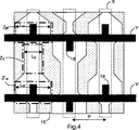
実施形態の第1ファミリーに従って、本発明に従ったプラズマディスプレイパネルは、図3に示すように、列分離素子15が幅において変化する点で、図1A及び1Bを参照すする上記のディスプレイパネルと主に異なる。それ故、マトリクス放電トリガゾーンZM、Z´Mにおいて、即ち、維持電極Y、Y´の一とアドレス電極との間の交差部分において、測定されるセルの幅LMは、アドレスアレイの電極Xの間隔pに等しいか又はそれより大きい一方、広がりゾーンZEにおいて、即ち、維持電極間において測定されるセルの幅LEは、同じ間隔pより小さい。
In accordance with the first family of embodiments, the plasma display panel according to the present invention includes the display panel described above with reference to FIGS. 1A and 1B in that the
それ故、マトリクストリガリングすることによりコプレーナ放電を駆動するとき、マトリクス放電トリガゾーンにおけるアバランシェ利得は増加し、仮想陽光柱の広がりゾーンにおける放電の効率は増加する。
Therefore, when driving a coplanar discharge by matrix triggering, the avalanche gain in the matrix discharge trigger zone increases and the efficiency of the discharge in the spreading zone of the virtual positive column increases.
パネルのセルは、セルの広い部分、即ち、マトリクス放電ゾーンを最適に分布させるように、互いに対して千鳥状に配列されている。それ故、図3に示すように、パネルの隣接していない列に属するセルの各々のマトリクス放電ゾーンは、隣接列のセル(図3におけるZ´´Mの場合)の広がりゾーン間か又は、それらの隣接列における異なる行の2つのセルを分離するゾーン間にある。それ故、ディスプレイパネルの何れの1つの列のセルは、隣接列のセルに関して列の一般方向において埋め合わせされている。 The cells of the panel are arranged in a staggered manner relative to each other so as to optimally distribute the wide portion of the cells, i.e. the matrix discharge zones. Therefore, as shown in FIG. 3, each matrix discharge zone of cells belonging to non-adjacent columns of the panel is between the spreading zones of cells in adjacent columns (in the case of Z ″ M in FIG. 3) or Between the zones separating two cells in different rows in their adjacent columns. Therefore, the cells in any one column of the display panel are filled in the general direction of the column with respect to the cells in the adjacent column.
この実施形態のファミリーは、例えば、画像表示コントラストを改善するように意図され、バリアリブの上部に位置付けられたブラックマトリクスの有効領域を更に増加させる。これは、低透過率ニュートラルフィルタを用いることを可能にし、プラズマディスプレイパネルの最終的な発光効率を更に改善する。 This family of embodiments, for example, is intended to improve the image display contrast and further increases the effective area of the black matrix located on top of the barrier ribs. This makes it possible to use a low transmittance neutral filter and further improves the final luminous efficiency of the plasma display panel.
セルの千鳥状配列は、図3に示すように、曲がりくねった、非直線的なプロファイルを有する維持電極をもたらす。 The staggered arrangement of cells results in a sustain electrode having a tortuous, non-linear profile, as shown in FIG.
図4は、図3に示しているディスプレイパネルの変形であって、セルが又千鳥状に配列されているが、維持電極は直線的である、変形を示している。維持電極Y、Y´は、ここでは、マトリクス放電ゾーンZM、Z´Mの中心の方に延びている枝18を備えている。それらの枝は、ITOのような透明な導電性材料から構成することが可能である。 FIG. 4 shows a variation of the display panel shown in FIG. 3, in which the cells are also arranged in a staggered fashion, but the sustain electrodes are linear. Sustain electrodes Y, Y'is here provided with a matrix discharge zone Z M, branches extending towards the center of the Z'M 18. The branches can be composed of a transparent conductive material such as ITO.
本発明の実施形態の第2ファミリーに従って、本発明に従ったプラズマディスプレイパネルは、図5に示すように、平行状態にある2つの広がりゾーンZE1、ZE2を得るように、維持電極Y、Y´間のみに広がっているセル間分離素子19を各々のセルが備えている点で、図1A及び1Bを参照した上記のディスプレイパネルと主に異なっている。ディスプレイパネルの発光効率は、それ故、更に改善される。この分離要素の寸法及び材料は、セルの壁素子、即ち、分離素子15、19の非常に近くにプラズマをもたらすように、正の擬似列を2つに分割するこれを得るために、それ自体既知である方式で設計されている。実際には、セル間分離素子19は、セル間分離素子15のように、バリアリブのアレイに統合され、同時に及び同じ材料で製造される。実際には、セル間分離素子19の幅は40μmに等しいか又はそれより大きい。
According to a second family of embodiments of the present invention, a plasma display panel according to the present invention, as shown in FIG. 5, to obtain the two spreading zones Z E1, Z E2 in the parallel state, sustain electrodes Y, This is mainly different from the display panel described above with reference to FIGS. 1A and 1B in that each cell includes an
マトリクス放電ゾーンの外側の維持電極間のみにそれらのセル間分離素子を位置付けることにより、たとえ、セル間分離素子15間の距離が、実際には、セルの全長に亘って一定であるとしても、得られるものは、広がりゾーンのセルの交差部分における縮小である。それ故、マトリクス放電ゾーンZM、Z´Mにおけるセルの幅LMは、各々の広がりゾーンZE1、ZE2の幅LE1、LZE2より大きい。
By positioning those inter-cell separation elements only between the sustain electrodes outside the matrix discharge zone, even though the distance between the
このような本発明の実施形態の第2ファミリーは又、特に、セル間の側壁またはセル間分離素子においてセル内の蛍光体のために利用可能な領域を増加させることを可能にするため、第1ファミリーより有利である。蛍光体層は図中に示していないことに留意する必要がある。このような蛍光体のための利用可能領域の増加は発光効率を改善するために支援する。
Such a second family of embodiments of the present invention also makes it possible to increase the area available for phosphors in the cell, particularly in the inter-cell sidewalls or inter-cell isolation elements . It is more advantageous than one family. It should be noted that the phosphor layer is not shown in the figure. Increasing the available area for such phosphors helps to improve luminous efficiency.
製造における制限のために、セルの列間間隔pは、2つの広がりゾーンZE1、ZE2の間の蛍光体の堆積と干渉する可能性がある。それ故、図6に示すように、千鳥状のセルの配列を使用することは好ましい。このような図5に示しているディスプレイパネルのバージョンにおいては、各々の維持電極はセルの2つの連続する行のために同時に役立つ。 Due to manufacturing limitations, the inter-column spacing p can interfere with phosphor deposition between the two spreading zones Z E1 , Z E2 . Therefore, it is preferable to use an array of staggered cells as shown in FIG. In such a version of the display panel shown in FIG. 5, each sustain electrode serves simultaneously for two consecutive rows of cells.
セル当たり1つのみのアドレス電極Xが存在する場合、電極における誘電体の厚さを増加させ、それ故、陽極容量を減少させ、それにより、陽光柱の形成を向上させ及び電子広がり速度を増加させるために、図5及び6に示すように、セル間分離素子19の下にこの電極を位置付けることは有利である。
When there is only one address electrode X per cell, it increases the thickness of the dielectric at the electrode, thus reducing the anode capacity, thereby improving the formation of positive columns and increasing the electron spreading rate In order to achieve this, it is advantageous to position this electrode under the
上記の実施形態の両方のファミリーにおいては、異なる列の2つのセルを分離するゾーンでは、それらのセルを区切るセル間分離素子間の隔たりは減少するが、0にはならない。この隔たりは、列において蛍光体を堆積することを容易にする凹部を有利に与えるために、広がりゾーンLE、LE1、LE2の幅より小さく、0ではなく、それにより、バリアリブの上部において蛍光体を堆積するリスクを低減する。 In both families of the above embodiments, in the zone separating two cells in different columns, the separation between the inter-cell separating elements that separate the cells is reduced, but not zero. This separation is advantageously less than the width of the spreading zones LE, LE1, LE2 and not 0, in order to advantageously provide a recess that makes it easier to deposit the phosphor in the row, so that the phosphor is not at the top of the barrier rib. Reduce the risk of deposition.
上記のプラズマディスプレイパネルはそれ自体既知である方法により製造されることが可能であるが、それについては、ここでは、説明しない。 The above plasma display panel can be manufactured by a method known per se, which will not be described here.
本発明は、同時提出の特許請求の範囲における範囲から逸脱することなく、プラズマディスプレイパネルの他の種類に適用することが可能である。 The present invention can be applied to other types of plasma display panels without departing from the scope of the appended claims.
上記のプラズマディスプレイパネルは、特に、各々の維持放電がマトリクス放電によりトリガされる維持動作を実行するための電力供給及び駆動手段を有するディスプレイに有利に統合される。そのような電力供給及び駆動手段は当業者には周知であり、例えば、上記の特許文献、米国特許第6,184,848号明細書において非常に詳細に記載されている。 The plasma display panel described above is particularly advantageously integrated into a display having power supply and drive means for performing a sustain operation in which each sustain discharge is triggered by matrix discharge. Such power supply and drive means are well known to those skilled in the art and are described in great detail, for example, in the above-mentioned patent document, US Pat. No. 6,184,848.
Claims (5)
前記第1プレートと第2プレートの間には放電ガスで満たされた空間が設けられ、
前記空間は、バリアリブのアレイにより行列状に配列された複数の放電セルに区分化され、
前記第1プレートは、維持電極と呼ばれるコプレーナ電極の少なくとも2つのアレイを有し、
前記維持電極は互いに平行で、かつ前記行に対して平行である一般方向に沿って方向付けられ、
前記維持電極は、誘電層及び保護層である2次電子放出層によってコーティングされ、
前記第2プレートは、アドレス電極と呼ばれる電極の少なくとも1つのアレイを有し、
前記アドレス電極は互いに平行で、かつ前記列に対して平行である一般方向に沿って方向付けられ、
前記電極は、各々のセルにおいて、アドレス電極が各々の維持電極のアレイと交差するように位置付けられ、
前記のバリアリブのアレイは列間分離素子を有し、
前記列間分離素子の各々は2つの隣接するセルの列を分離し、
各セルは、各々が維持電極と前記アドレス電極の交差部分において位置している少なくとも2つのトリガゾーン、及び、前記トリガゾーン間において広がっている少なくとも2つのコプレーナ放電広がりゾーンに再分割され、
前記バリアリブのアレイは複数の列間分離素子を有し、
該列間分離素子の各々は2つの隣接するセルの列を分離し、
各々のセルは、前記トリガゾーン間にある前記隔たり内の列の方向に沿って広がり、前記セルの2つの隣接するコプレーナ放電広がりゾーンを区分化する少なくとも1つのセル内分離素子により再分割され、
前記列間分離素子及びセル内分離素子の各々の設計は、
各々のセルにおいて、前記2つの隣接するコプレーナ放電広がりゾーンが、前記列に沿って画定される前記トリガゾーン間にある隔たりの範囲内にある幅を有し、かつ
該幅は、前記行に沿って画定される2つの隣接する分離素子間で測定されるときには、前記列に沿って前記トリガゾーンを画定する2つの隣接する列間分離素子間で測定される前記トリガゾーンの全ての幅よりも狭くなる、
ように行われ、
当該プラズマディスプレイパネルを有する画像ディスプレイ装置は、当該ディスプレイパネルの電極を駆動及び供給する手段を有し、前記手段は、前記セルを交差する種々のコプレーナ電極間でのコプレーナ放電を各セル内で発生させるのに適する前記コプレーナ電極へ維持電圧信号を付与し、かつ、各維持電圧信号を付与する前又は間に、前記セルを交差するアドレス電極と前記コプレーナ電極のうちの1つとの間でのトリガ電圧信号を付与することが可能で、前記コプレーナ放電はそれぞれ前記トリガ電圧信号によって発生するマトリックス放電によって引き起こされる、
ことを特徴とするプラズマディスプレイパネル。A plasma display panel having a first plate and a second plate,
A space filled with a discharge gas is provided between the first plate and the second plate,
The space is partitioned into a plurality of discharge cells arranged in a matrix by an array of barrier ribs,
The first plate has at least two arrays of coplanar electrodes, called sustain electrodes,
The sustain electrodes are oriented along a general direction that is parallel to each other and parallel to the rows;
The sustain electrode is coated with a secondary electron emission layer that is a dielectric layer and a protective layer,
The second plate has at least one array of electrodes called address electrodes;
The address electrodes are oriented along a general direction parallel to each other and parallel to the columns;
The electrodes are positioned in each cell such that the address electrodes intersect each array of sustain electrodes;
The array of barrier ribs has inter-row separation elements ;
Each of said inter-row separation element separates the columns of two adjacent cells,
Each cell is subdivided into at least two trigger zones, each located at the intersection of the sustain electrode and the address electrode, and at least two coplanar discharge spreading zones extending between the trigger zones;
The array of barrier ribs has a plurality of inter-row separation elements ,
Each of the inter-column separators separates two adjacent columns of cells;
Each cell, spreads along the direction of the column in the gap existing between the trigger zone is subdivided by at least one cell isolation elements for partitioning the two adjacent coplanar discharge expansion zone of said cell,
Each design of the inter-column separation element and the intra-cell separation element is as follows:
In each cell, the two adjacent coplanar discharge spreading zones have a width that is within a distance between the trigger zones defined along the column, and the width is along the row When measured between two adjacent separation elements that are defined in greater than the entire width of the trigger zone measured between two adjacent separation elements that define the trigger zone along the column. Narrow,
Done as
The image display apparatus having the plasma display panel has means for driving and supplying the electrodes of the display panel, and the means generates coplanar discharge between various coplanar electrodes crossing the cell in each cell. Applying a sustain voltage signal to the coplanar electrodes suitable for causing and triggering between the address electrode and one of the coplanar electrodes crossing the cell before or during each sustain voltage signal application A voltage signal can be applied, and each of the coplanar discharges is caused by a matrix discharge generated by the trigger voltage signal ,
A plasma display panel characterized by that.
Applications Claiming Priority (3)
| Application Number | Priority Date | Filing Date | Title |
|---|---|---|---|
| FR0306305 | 2003-05-26 | ||
| FR0306305A FR2855646A1 (en) | 2003-05-26 | 2003-05-26 | PLASMA DISPLAY PANEL WITH REDUCED SECTION DISCHARGE EXPANSION AREA |
| PCT/FR2004/050207 WO2004107385A2 (en) | 2003-05-26 | 2004-05-26 | Plasma display panel comprising a reduced-section discharge expansion zone |
Publications (3)
| Publication Number | Publication Date |
|---|---|
| JP2007500928A JP2007500928A (en) | 2007-01-18 |
| JP2007500928A5 JP2007500928A5 (en) | 2010-06-17 |
| JP4898443B2 true JP4898443B2 (en) | 2012-03-14 |
Family
ID=33427417
Family Applications (1)
| Application Number | Title | Priority Date | Filing Date |
|---|---|---|---|
| JP2006530445A Expired - Fee Related JP4898443B2 (en) | 2003-05-26 | 2004-05-26 | Plasma display panel having a reduced section discharge spreading zone |
Country Status (10)
| Country | Link |
|---|---|
| US (1) | US7768199B2 (en) |
| EP (1) | EP1627408B1 (en) |
| JP (1) | JP4898443B2 (en) |
| KR (1) | KR101067842B1 (en) |
| CN (1) | CN100524591C (en) |
| DE (1) | DE602004016319D1 (en) |
| FR (1) | FR2855646A1 (en) |
| MX (1) | MXPA05012333A (en) |
| TW (1) | TWI329332B (en) |
| WO (1) | WO2004107385A2 (en) |
Families Citing this family (1)
| Publication number | Priority date | Publication date | Assignee | Title |
|---|---|---|---|---|
| CN101707173B (en) * | 2009-11-06 | 2011-11-30 | 山东大学 | Three-dimensional stereo plasma display component |
Citations (7)
| Publication number | Priority date | Publication date | Assignee | Title |
|---|---|---|---|---|
| JPH09160525A (en) * | 1995-08-03 | 1997-06-20 | Fujitsu Ltd | Plasma display panel, its driving method, and plasma display device |
| JPH11143425A (en) * | 1997-11-13 | 1999-05-28 | Ttt:Kk | Driving method of ac type pdp |
| JPH11317171A (en) * | 1998-02-27 | 1999-11-16 | Koninkl Philips Electronics Nv | Plasma display |
| JP2001052618A (en) * | 1999-08-03 | 2001-02-23 | Matsushita Electric Ind Co Ltd | Ac type plasma display panel and its driving method |
| JP2001325891A (en) * | 2000-05-19 | 2001-11-22 | Nippon Hoso Kyokai <Nhk> | Direct-current discharge type plasma display panel |
| JP2005515590A (en) * | 2002-01-14 | 2005-05-26 | プラズミオン・ディスプレイズ・リミテッド・ライアビリティ・カンパニー | Plasma display panel having trench discharge cells and manufacturing method thereof |
| JP2005531110A (en) * | 2002-06-24 | 2005-10-13 | トムソン プラズマ | Coplanar discharge electrode plate for plasma display panel providing adapted surface potential distribution |
Family Cites Families (9)
| Publication number | Priority date | Publication date | Assignee | Title |
|---|---|---|---|---|
| JP3719743B2 (en) * | 1995-08-09 | 2005-11-24 | 株式会社日立製作所 | Plasma display panel |
| US6853138B1 (en) * | 1999-11-24 | 2005-02-08 | Lg Electronics Inc. | Plasma display panel having grooves in the dielectric layer |
| JP4158874B2 (en) * | 2000-04-07 | 2008-10-01 | 株式会社日立プラズマパテントライセンシング | Image display method and display device |
| JP3659913B2 (en) | 2001-10-30 | 2005-06-15 | 富士通株式会社 | Plasma display panel and manufacturing method thereof |
| US6737804B2 (en) * | 2002-03-21 | 2004-05-18 | Chungwa Picture Tubes | Barrier rib structure for plasma display panel |
| JP2004272199A (en) * | 2003-02-18 | 2004-09-30 | Fuji Xerox Co Ltd | Rib for image display medium, method for manufacturing the same, and image display medium using the same |
| TWI247325B (en) * | 2003-06-27 | 2006-01-11 | Chunghwa Picture Tubes Ltd | Barrier rib structure for plasma display panel |
| TWI222657B (en) * | 2003-08-27 | 2004-10-21 | Au Optronics Corp | Plasma display panel |
| KR100749613B1 (en) * | 2005-06-14 | 2007-08-14 | 삼성에스디아이 주식회사 | Plasma display panel |
-
2003
- 2003-05-26 FR FR0306305A patent/FR2855646A1/en active Pending
-
2004
- 2004-05-21 TW TW093114356A patent/TWI329332B/en not_active IP Right Cessation
- 2004-05-26 DE DE602004016319T patent/DE602004016319D1/en active Active
- 2004-05-26 MX MXPA05012333A patent/MXPA05012333A/en active IP Right Grant
- 2004-05-26 KR KR1020057022504A patent/KR101067842B1/en not_active IP Right Cessation
- 2004-05-26 WO PCT/FR2004/050207 patent/WO2004107385A2/en active IP Right Grant
- 2004-05-26 EP EP04742875A patent/EP1627408B1/en not_active Expired - Fee Related
- 2004-05-26 JP JP2006530445A patent/JP4898443B2/en not_active Expired - Fee Related
- 2004-05-26 CN CNB2004800144572A patent/CN100524591C/en not_active Expired - Fee Related
- 2004-05-26 US US10/558,037 patent/US7768199B2/en not_active Expired - Fee Related
Patent Citations (7)
| Publication number | Priority date | Publication date | Assignee | Title |
|---|---|---|---|---|
| JPH09160525A (en) * | 1995-08-03 | 1997-06-20 | Fujitsu Ltd | Plasma display panel, its driving method, and plasma display device |
| JPH11143425A (en) * | 1997-11-13 | 1999-05-28 | Ttt:Kk | Driving method of ac type pdp |
| JPH11317171A (en) * | 1998-02-27 | 1999-11-16 | Koninkl Philips Electronics Nv | Plasma display |
| JP2001052618A (en) * | 1999-08-03 | 2001-02-23 | Matsushita Electric Ind Co Ltd | Ac type plasma display panel and its driving method |
| JP2001325891A (en) * | 2000-05-19 | 2001-11-22 | Nippon Hoso Kyokai <Nhk> | Direct-current discharge type plasma display panel |
| JP2005515590A (en) * | 2002-01-14 | 2005-05-26 | プラズミオン・ディスプレイズ・リミテッド・ライアビリティ・カンパニー | Plasma display panel having trench discharge cells and manufacturing method thereof |
| JP2005531110A (en) * | 2002-06-24 | 2005-10-13 | トムソン プラズマ | Coplanar discharge electrode plate for plasma display panel providing adapted surface potential distribution |
Also Published As
| Publication number | Publication date |
|---|---|
| EP1627408B1 (en) | 2008-09-03 |
| EP1627408A2 (en) | 2006-02-22 |
| FR2855646A1 (en) | 2004-12-03 |
| MXPA05012333A (en) | 2006-05-31 |
| WO2004107385A3 (en) | 2005-01-27 |
| JP2007500928A (en) | 2007-01-18 |
| TW200504781A (en) | 2005-02-01 |
| CN100524591C (en) | 2009-08-05 |
| KR101067842B1 (en) | 2011-09-27 |
| WO2004107385A2 (en) | 2004-12-09 |
| TWI329332B (en) | 2010-08-21 |
| CN1795525A (en) | 2006-06-28 |
| DE602004016319D1 (en) | 2008-10-16 |
| US7768199B2 (en) | 2010-08-03 |
| US20070241996A1 (en) | 2007-10-18 |
| KR20060028764A (en) | 2006-04-03 |
Similar Documents
| Publication | Publication Date | Title |
|---|---|---|
| CN100377281C (en) | Coplanar discharge faceplates for plasma display panel providing adapted surface potential distribution | |
| KR100502910B1 (en) | Plasma display panel having delta pixel arrangement | |
| JP2001195985A (en) | Flat panel display having controlled maintenance electrode | |
| JP4184949B2 (en) | Driving method of plasma panel with coplanar sustain discharge between triplet structure electrodes | |
| JP4898443B2 (en) | Plasma display panel having a reduced section discharge spreading zone | |
| JP3123053B2 (en) | Gas discharge display element and driving method thereof | |
| US20050212428A1 (en) | Plasma display panel | |
| KR20040031694A (en) | Method for monitoring a coplanar plasma display panel using a pulse train with sufficiently high frequency to stabilise the discharges | |
| JP4430542B2 (en) | Plasma display panel | |
| US7598673B2 (en) | Plasma display panel with enhanced luminous efficiency at a reduced discharge firing voltage | |
| JPH09259767A (en) | Ac type pdp and driving method therefor | |
| KR100404080B1 (en) | Structure of hybrid plasma display panel device | |
| JP2001028243A (en) | High-frequency driving plasma display panel and drive device thereof | |
| JP3641762B2 (en) | Discharge display device | |
| KR100381263B1 (en) | Electrode Structure Of Plasma Display Panel and Method of Driving Sustain Electrode in The Plasma Display Panel | |
| KR100684723B1 (en) | A plasma display panel and driving method of the same | |
| KR100589388B1 (en) | Plasma display panel | |
| KR100719592B1 (en) | Plasma display panel | |
| KR100326857B1 (en) | Fabricating Method of Plasma Display Panel Driving with Radio Frequency Signal | |
| KR100599626B1 (en) | A plasma display panel and driving method of the same | |
| KR100778410B1 (en) | Plasma display panel | |
| KR20050052201A (en) | Plasma display panel | |
| KR20050119909A (en) | Plasma display panel | |
| KR20000065279A (en) | Plasma display panel using high frequency | |
| KR20050122537A (en) | Plasma display panel |
Legal Events
| Date | Code | Title | Description |
|---|---|---|---|
| A621 | Written request for application examination |
Free format text: JAPANESE INTERMEDIATE CODE: A621 Effective date: 20070521 |
|
| A977 | Report on retrieval |
Free format text: JAPANESE INTERMEDIATE CODE: A971007 Effective date: 20100115 |
|
| A131 | Notification of reasons for refusal |
Free format text: JAPANESE INTERMEDIATE CODE: A131 Effective date: 20100126 |
|
| A521 | Written amendment |
Free format text: JAPANESE INTERMEDIATE CODE: A523 Effective date: 20100421 |
|
| A524 | Written submission of copy of amendment under section 19 (pct) |
Free format text: JAPANESE INTERMEDIATE CODE: A524 Effective date: 20100421 |
|
| A131 | Notification of reasons for refusal |
Free format text: JAPANESE INTERMEDIATE CODE: A131 Effective date: 20100622 |
|
| A521 | Written amendment |
Free format text: JAPANESE INTERMEDIATE CODE: A523 Effective date: 20100922 |
|
| A02 | Decision of refusal |
Free format text: JAPANESE INTERMEDIATE CODE: A02 Effective date: 20110118 |
|
| A521 | Written amendment |
Free format text: JAPANESE INTERMEDIATE CODE: A523 Effective date: 20110518 |
|
| A911 | Transfer to examiner for re-examination before appeal (zenchi) |
Free format text: JAPANESE INTERMEDIATE CODE: A911 Effective date: 20110526 |
|
| A131 | Notification of reasons for refusal |
Free format text: JAPANESE INTERMEDIATE CODE: A131 Effective date: 20110802 |
|
| A521 | Written amendment |
Free format text: JAPANESE INTERMEDIATE CODE: A523 Effective date: 20110909 |
|
| TRDD | Decision of grant or rejection written | ||
| A01 | Written decision to grant a patent or to grant a registration (utility model) |
Free format text: JAPANESE INTERMEDIATE CODE: A01 Effective date: 20111213 |
|
| A01 | Written decision to grant a patent or to grant a registration (utility model) |
Free format text: JAPANESE INTERMEDIATE CODE: A01 |
|
| A61 | First payment of annual fees (during grant procedure) |
Free format text: JAPANESE INTERMEDIATE CODE: A61 Effective date: 20111226 |
|
| R150 | Certificate of patent or registration of utility model |
Free format text: JAPANESE INTERMEDIATE CODE: R150 |
|
| FPAY | Renewal fee payment (event date is renewal date of database) |
Free format text: PAYMENT UNTIL: 20150106 Year of fee payment: 3 |
|
| LAPS | Cancellation because of no payment of annual fees |