JP4889152B2 - Electromagnetic field generator and method of operation - Google Patents
Electromagnetic field generator and method of operation Download PDFInfo
- Publication number
- JP4889152B2 JP4889152B2 JP2000569422A JP2000569422A JP4889152B2 JP 4889152 B2 JP4889152 B2 JP 4889152B2 JP 2000569422 A JP2000569422 A JP 2000569422A JP 2000569422 A JP2000569422 A JP 2000569422A JP 4889152 B2 JP4889152 B2 JP 4889152B2
- Authority
- JP
- Japan
- Prior art keywords
- magnetic
- current
- electromagnetic
- magnetic field
- assembly
- Prior art date
- Legal status (The legal status is an assumption and is not a legal conclusion. Google has not performed a legal analysis and makes no representation as to the accuracy of the status listed.)
- Expired - Fee Related
Links
Images


Classifications
-
- H—ELECTRICITY
- H01—ELECTRIC ELEMENTS
- H01J—ELECTRIC DISCHARGE TUBES OR DISCHARGE LAMPS
- H01J37/00—Discharge tubes with provision for introducing objects or material to be exposed to the discharge, e.g. for the purpose of examination or processing thereof
- H01J37/32—Gas-filled discharge tubes
- H01J37/32431—Constructional details of the reactor
- H01J37/32623—Mechanical discharge control means
-
- H—ELECTRICITY
- H01—ELECTRIC ELEMENTS
- H01J—ELECTRIC DISCHARGE TUBES OR DISCHARGE LAMPS
- H01J37/00—Discharge tubes with provision for introducing objects or material to be exposed to the discharge, e.g. for the purpose of examination or processing thereof
- H01J37/30—Electron-beam or ion-beam tubes for localised treatment of objects
- H01J37/317—Electron-beam or ion-beam tubes for localised treatment of objects for changing properties of the objects or for applying thin layers thereon, e.g. for ion implantation
- H01J37/3178—Electron-beam or ion-beam tubes for localised treatment of objects for changing properties of the objects or for applying thin layers thereon, e.g. for ion implantation for applying thin layers on objects
-
- H—ELECTRICITY
- H01—ELECTRIC ELEMENTS
- H01J—ELECTRIC DISCHARGE TUBES OR DISCHARGE LAMPS
- H01J37/00—Discharge tubes with provision for introducing objects or material to be exposed to the discharge, e.g. for the purpose of examination or processing thereof
- H01J37/32—Gas-filled discharge tubes
- H01J37/32431—Constructional details of the reactor
- H01J37/3266—Magnetic control means
Landscapes
- Chemical & Material Sciences (AREA)
- Analytical Chemistry (AREA)
- Physics & Mathematics (AREA)
- Engineering & Computer Science (AREA)
- Plasma & Fusion (AREA)
- Physical Vapour Deposition (AREA)
- Physical Deposition Of Substances That Are Components Of Semiconductor Devices (AREA)
- Manufacturing Of Magnetic Record Carriers (AREA)
- Thin Magnetic Films (AREA)
Description
【0001】
(発明の分野)
本発明は磁性材料の堆積に関する。更に詳細には、本発明は、磁性材料の堆積を改良するための電磁界発生器および操作方法に関する。
【0002】
(発明の背景)
堆積方式(例えば、イオンビーム、物理的蒸気、および、蒸着)は、多くの異なるタイプの基質上に多種多様な材料の高品質薄膜を堆積することが可能である。例えば、薄膜磁気ヘッドに用いられる磁気抵抗性(MR)および巨大磁気抵抗性(GMR)薄膜の堆積のような強磁性薄膜への適用では、通常、外部磁界の印加により磁気モーメントを特定方向に向けることを必要とする。必要とされる磁界強度は通常20−100ガウスである。
【0003】
しかしながら、磁界とプラズマの間の相互作用の故に、プラズマデポジション(蒸着)方式に対しては、DC磁界は面倒であることが発見されている。この種の相互作用は、例えば、プラズマの均一性が低下する結果として、堆積された磁気薄膜の厚さの均一性を低下させる。10−15ガウス程度の低レベルであってさえも、磁界とイオンビームとの相互作用に起因して、堆積チャンバ内における磁界がイオンビーム堆積処理に悪影響を及ぼすことも、我々は発見している。イオンビームデポジションに際して、磁界妨害は、薄膜汚染を引き起こすイオンビームを広げる作用、又は、変位させる作用の原因となる。更に、通常、基質上に蓄積されたあらゆる電荷を中和するように作用するイオンビームチャンバ内の電子は磁界によって極く容易にトラップされ得る。この種のトラップ作用は、基質上の露出されたあらゆる絶縁表面、又は、例えば磁気抵抗センサなどの、基質ウェーハに埋め込まれたあらゆる静電放電感応デバイス構造の中和作用のロスを引き起こす。イオン支援堆積処理が用いられる場合には支援イオンビームが基質を直撃するので、前述のトラップ作用の影響は特に重要である。
【0004】
磁界発生源を妨害することなしに、または、サンプル上またはチャンバ内に電荷を蓄積させることなしに支援磁界が存在する堆積システムにおける磁性材料堆積方法が必要とされる。
【0005】
(発明の概要)
本発明に従って、磁性材料堆積のための電磁界発生器および操作方法について記述する。電磁界発生器は、基質上に第1の方向の磁界を生じさせるために間隔を保持して配置された第1対(ペア)の磁気部材および基質上に第2の方向の磁界を生じさせるために間隔を保持して配置された第2対の磁気部材を備えたオープンフレーム電磁アセンブリを有する。電磁界発生器は、第1アセンブリと間隔を保って配置され、基質上の磁界均一性を強化するために第1アセンブリに磁気的に組み合わされた第2電磁アセンブリを有することが好ましい。本方法が含むステップを次に示す。即ち、少なくとも2つの選択可能な磁界配向を持つ電磁界発生器内にサンプルを置くステップと、電磁界発生器によって影響されるサンプル上に材料を堆積するための例えばイオン源またはプラズマ源などの供給源を操作するステップと、電磁界発生器を用いて磁性材料の堆積を制御するためにサンプルの周りに磁界パターンを生成するステップである。
【0006】
電磁界発生器に供給される異なる電流信号により、結果として異なる磁界を発生することで、堆積した材料を制御する様々な方法についても記述する。電流には、交流電流、パルス化された正/負直流電流、指数的に減衰する交流電流、半波整流された交流電流、パルス化された正の直流、正の直流バイアス、正の直流電流バイアスを持つパルス化された直流、時間的に整相された磁界およびイオン発生器操作電流が含まれる。
【0007】
一目的は、オープンフレーム/ベースプレートを組合わせた電磁界発生器が一辺6インチの正方形または直径8インチの円形全体に亙る許容角度が0.5度である測定された磁界方向性を供給することにある。これは、最小限度の方向性誤差をもつ配向された磁気薄膜の堆積を可能にする。
【0008】
更に別の一目的は、異なる方向に配向された磁気薄膜の交互配置された層の堆積を可能にする任意のあらゆる方向に磁界を方向付けする能力を提供することにある。
【0009】
更に他の一目的は、堆積された薄膜を消磁するために、磁界の配向を回転するように連続的に変更する能力を提供することにある。
【0010】
更に別の一目的は、サンプル全体に亙って磁界均一性が+/−5%の均一な磁界領域を提供することにある。
【0011】
更に他の一目的は、オープンフレーム最上部プレートの隅を切り欠くことによって重量を軽減することにある。隅を切り欠くことにより、磁界発生器を収容するために、チャンバ内に必要とされるスペースの対角部の寸法も減少する。オープンフレーム設計は、電磁界発生器が能動堆積部位を包囲し、それによって、能動堆積部位を邪魔しない状態に保持することも可能にする。従って、電磁界発生器はスパッタリングされた材料が蓄積することから保護される。これは、磁界発生器をピーク稼働状態に維持するために必要な保守整備レベルを低くする。
【0012】
本発明全体がここに要約されることを意図するものでなく、本発明の特徴、態様、及び、利点は以下の記述および図面に記載されていて、これらから明白である。
【0013】
【発明の実施の形態】
本発明は様々な代替実施形態を用いて、装置について記述し、また、材料堆積を制御する操作方法について記述する。
【0014】
(装置)
基質(基板)、ウェーハ、及び、サンプル(標本)という用語は、本明細書を通じて互換可能に用いられるものとする。オープンフレーム部材(メンバ)という用語は記述的であって、本明細書及び特許請求の範囲内においては更に大きい開口部位を有する部材を表すことを意図するものである。従って、オープンフレーム部材は実質的に中実(中空でない)な部材と対照され、実質的に中実である部材はオープンフレーム部材よりも小さい開口部位を持つものと理解される。「実質的」または「実質的に」という用語も本明細書および特許請求の範囲において用いられ、特定の定量的定義を一切用いることなしに幾らかの改変を許容する用語であることを意図するものである。
【0015】
先ず図1では、本発明に係る電磁界発生器の第1実施形態が図示される。詳細に記述すれば、本発生器は、基板115上に第1方向の磁界を生成するために間隔を保って配置された第1の対(ペア)の磁気部材120と、基板上に第2方向の磁界を生成するために間隔を保って配置された第2の対(ペア)の磁気部材130を備えたオープンフレーム部材110を有する。第1磁界と第2磁界が直交するように磁気部材120は磁気部材130に垂直に配置されることが好ましい。オープンフレーム110は、例えば、様々な軟鋼のうちのいずれかによって構成されてもよい。
【0016】
図11A及び11Bを参照すると、コイル120と130の直交対は、直角に配向された磁気薄膜の堆積を可能とするように選択的に駆動される。図11Aにおいて、コイル120が電力供給されるときには、第1の方向に磁界が形成される。図11Bにおいて、コイル130が電力供給されるときには、第2の方向に磁界が形成される。両コイルに同時に電力を供給すると、2つのコイルに流れる電流の比率に比例した方向性を持つ任意の磁界配向を生じる。
【0017】
図2は、本発明の第2の実施形態に係る4コイル2オープンフレーム電磁界発生器の斜視図である。コイル210と215は、中央開口部240内に磁界を誘起するようにオープンフレーム部材220と230に巻きつけられる。対向するコイル対210と215を用いて直角に方向付けされた磁界が付加される。誘起された磁界は、中央開口部240内において最も均一であるが、ウェーハ又は基質(図示されず)が最も好適に配置される位置である開口部の上の位置にも伸延する。各隅に配置される4個の磁極片250は、電磁界の整形を助け、特に中央開口部240の上の磁界の均一性を増大させる。磁極片250は、例えば、軟鋼によって構成される。他の構成要素とともにパッケージに実装するために、オープンフレーム部材220及び230は角を丸めるか又は切り欠いても差し支えない。
【0018】
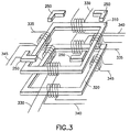
本発明の第3の実施形態に従って磁極片250を備えた図3は、8コイル2オープンフレーム電磁界発生器の斜視図である。この実施形態は、図2に示す第2実施形態と異なり、オープンフレーム310にはコイル対330と335が巻き付けられ、オープンフレーム320にはコイル対340と345が巻き付けられる。各オープンフレームに関して個別コイルを用いることにより、この実施形態においては、各コイルを流れる電流の個別制御を可能にし、それにより、各コイルによって生成される磁界全体に亙り制御性が向上される。他の構成要素とともにパッケージに実装するために、オープンフレーム310と320は角を丸めるか又は切り欠いても差し支えない。
【0019】
図2および図3に示す実施形態の代替実施形態において、電気巻線210、215、330、335、340、345は、埋め込まれた巻線またはパターン化された電極により置き換え可能である。
【0020】
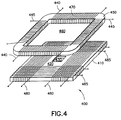
図4は8コイル2オープンフレーム電磁界発生器の斜視図である。この構成において、電磁界発生器400は、中央開口部430を有するベースプレート410を備える。この構成において、中央開口部430はウェーハチャック(図示せず)及び他の機械的および電気的フィードスルー(貫通部品)を収容する。中央開口部430は、機械的接続のために、巻線のない領域420によって囲まれている。ベースプレート410の残りの部分には、既に説明したように直交磁界を誘起するために、コイル対480と485が巻き付けられることが好ましい。他の構成では、基質またはウェーハチャック及び必要なフィードスルーは電磁界発生器400の側方から支持され、中央開口部430をなくすことができる。
【0021】
図4において、オープンフレーム部材450は、基質上に第1の方向の磁界を生成するために間隔を保って配置される第1対の磁気部材440と、基質上に第2の方向の磁界を生成するために間隔を保って配置される第2対の磁気部材445とを有する。オープンフレーム部材450は中央開口部460を備える。他の構成要素とともにパッケージに実装するために、最上部プレート450は角を丸めるか又は切り欠いても差し支えない。最上部プレート450及びベースプレート410は、それらのプレートと他の機械的および電気的構成要素の間に基質またはウェーハチャックを収容するために、間隔を保って配置される。ベースプレート410は、サンプル上に更に均一な磁界を生成するために、最上部プレート450の磁力線を所要方向に補強し、他の方向における望ましくない成分を部分的にキャンセルするような方向に向けられた磁力線を有する。ベースプレート410は、最上部フレーム450によって提供される磁界を直線化および強化する。
【0022】
図4には磁極片が示されていないが、図2及び図3に示すように、磁極片を使用し、配向されても差し支えない。図4の装置と共に使用する場合には、磁極片は電磁界を整形し、装置の磁界の均一性を増加する。
【0023】
ウェーハチャック(図示せず)は、ウェーハが最上部プレート450によって作られた磁界の中央470の直ぐ上に位置するように中央開口部460内に配置されることが好ましい。これは、磁界の均一性に関して好ましい場所である。ただし、清浄性(スパッタリングされた材料が電磁界発生器に付着しないようにする)及びシャドウイングを含む他の要因を考慮すると、基質は、磁界の均一性を実質的に犠牲にすることなく磁界の中心部470の上に配置しても差し支えない。
【0024】
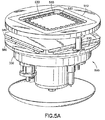
図5Aは、本発明の一実施形態に係る電磁界発生器およびウェーハチャックユニット500の斜視図である。オープンフレーム装置510は、オープンフレーム220(図2)または310(図3)または450(図4)の形をした磁界発生器の最上部プレートを収容する。この構成において、ウェーハ530は、誘起された磁界の中心のわずかに上であって、オープンフレーム装置510の中間平面のわずかに下に配置されることが好ましい。ウェーハ530は、ウェーハチャック560に添付されたクリップ520によって所定場所に保持される。
【0025】
オープンフレーム装置510は、水冷され、チャンバの基本圧力と大気の間の圧力、例えば、10-3Torrまで差動的にポンピングされる。オープンフレーム装置510は、カバープレート540上にサポート570によって支持される。サポート570の1つは中空であり、オープンフレーム装置510用の電気的および機械的なフィードスルーを収容する。カバープレート540は、電磁界発生器のオープンフレーム230(図2)または320(図3)またはベースプレート410(図4)を囲む。下側エレメントのタイプには関係なく、電磁界発生器のベース部分はカバープレート540の下方に所在し、電気巻線(図4における480および485)に関連した絶縁材料は真空チャンバにとって潜在的汚染物質であるので、まわりの真空チャンバから分離されるか又は大気圧に維持される。
【0026】
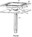
カバープレート540は、図5Aでは隠れて見えない中央開口部を備える。図5Bに示すように、ウェーハチャック560のシャフト555は、カバープレート540の開口部を貫通する。図5Aに示される残りの支持構造物550は、ウェーハチャックアセンブリの標準構成要素であるユニット500用として必要な機械的および電気的フィードスルーを収容することが好ましい。
【0027】
図5Bは、分かり易くするためにオープンフレーム装置510が露出された状態における、ウェーハチャック560および図5Aの電磁界発生器の最上部プレートの斜視図である。ウェーハシート565とベースプレート535の開口部545を貫くシャフト555によって支持された状態のウェーハチャック560が図示される。ベースプレート535は、オープンフレーム210(図2)、320(図3)、または、410(図4)の構成であっても差し支えない。一例として、電気巻線対440と445(図4)が図面から省略された状態のベースプレート構成410(図4)を示す。ウェーハシート565は、ウェーハ530の温度制御を維持するための加熱、及び/又は、冷却エレメントを含むこともあり得る。
【0028】
図5Aにおいて、電磁界発生器/ウェーハチャックユニット500の磁界発生に関係しない部分は非磁性材料製であることが好ましい。例えば、ウェーハチャック560、クリップ520、ウェーハシート(図5Bにおける565)、シャフト(図5Bにおける555)、カバープレート540、および、オープンフレーム装置510を含む、ウェーハから3ないし4インチの範囲内のウェーハを直接囲む構造体は、非磁性ステンレス鋼合金321、316、または310、アルミニウム、または、銅製であることが好ましい。ウェーハチャック560の残りの構造体は、同様に、これらの非磁性材料321、316、または310製であるか、又は、ステンレス鋼合金304製であっても差し支えない。ステンレス鋼合金304は、強い磁界に曝されると、経年的に磁化されるので、ウェーハ530の近くに配置するべきではない。
【0029】
ここに記載されている諸例では2磁気エレメント設計が用いられている。この場合、各磁気エレメントは異なる巻き回数「n」の磁化巻線を備え、エレメントを流れる最適電流「I」を供給するために個別電源によって電力供給される。この例および他の諸例のように、磁束が電流に比例する実施形態においては、軟質の磁気コアは最大電流において磁気的に飽和しないものと仮定する。そうでなければ、電流変化に比例して磁束が変化することは不可能である。
【0030】
更に別の一実施形態においては、各磁気エレメントに電源供給するために1つの単一電源が用いられる。あらゆる磁気エレメントが生成する磁束は「n」又は「I」のどちらかに正比例し、従って、磁気エレメント#1からの任意の点における磁束はn1およびI1に比例し、磁気エレメント#2からの任意の点における磁束はn2およびI2に比例する。従って、n1、n2、I1、及び、I2のあらゆる組合わせに関して、磁気エレメントが電流I2によって電力供給された場合に、巻回数n1で電流I1の場合と同じ磁束を生成するように、このエレメントにおける巻回数をn1からn1'に調節可能である。この方法によれば、両方の磁気エレメント用に同一電源を使用できる。
【0031】
必要とされる新規な巻回数は次式で算定できる。
【0032】
n1'=n1*I1/I2
本実施形態の一例において、I1が6アンペアでn1が185回、I2が8アンペアでn2が288回である場合に、同じ電源(I1=I2=8アンペア)を用いて、同じ結果を達成するためには、巻回数(n1)は6/8*n1即ち139回に変更される。
【0033】
上記の例ではただ2個の磁気エレメントが用いられたが、本技法は多数の磁気エレメントにも同様に適用されることに注意されたい。
【0034】
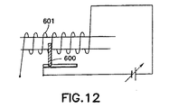
図12において、1つのコイルの実効巻回数を調節する簡単な方法を示す。摺動接点600は、実効巻回数を変えるように、コイル601に沿って接点を調節可能にする。図12に示す方法と類似の方法を用いて、図1、2、3、4、5A、5B、11A、または、11Bに示すあらゆるコイルの実効巻回数を調節可能である。この方法によれば、実効巻回数は広範囲に亙って変更可能であり、従って、単一電源を使用して、可変磁束を提供することが可能である。
【0035】
(操作方法)
本発明の一態様にしたがい、電磁界発生器は、堆積(デポジション)に際して、周期的またはパルス化された方法で駆動可能である。即ち、電磁界発生器へ印加される電流は周期的パターンでオン/オフを繰り返される。本発明の周期的方法のいくつかの実施形態を図6から図9に示す。これらの異なる方法は、一方向の1つの単一磁界生成に適用可能であり、或いは、2つの電源電流間の位相を制御することにより、異なる方向に磁界を生成するために使用可能である。
【0036】
図6(A)は、交流(AC)としての電磁界発生器電流を示す。図6(B)において、電磁界発生器電流は正および負(+/−)のパルス化された直流(DC)である。図6(C)は消磁手順用に振幅が指数的に減衰する図6(A)の交流電磁界発生器電流を示す。図7(A)は半波整流された交流電流を示す。図7(B)はパルス化された正(+)の直流電流を示す。図7(C)は正の直流電流バイアスを示す。その代りに負の直流電流バイアスを使用しても差し支えない。図8(A)は正の直流電流バイアスを用いる交流電流操作を示す。図8(B)は正の直流電流を用いるパルス化された直流電流操作を示す。図9は電磁界発生器とイオンビーム電流の間の位相差を用いるパルス化された正(+)の直流電流を示す。
【0037】
図6(A)の交流電流および図6(B)のパルス化された正および負(+/−)の直流電流は正味ゼロ平均磁界効果をイオンビームに提供し、例えばNiFeをベースとする薄膜、例えばNiFeCr、NiFeRh、NiFeTa、またはアモルファスCoをベースとする合金材料などの軟質隣接層(SAL)薄膜と共に最も有効に利用される。図6(C)は、磁気取付け具を以前に使用したことにより磁化された取付け具溶接の敏感な部品を消磁するために、基質と共に或いは基質なしで有利に利用可能な、振幅が指数的に減衰する交流電流を示す。
【0038】
図7(A)の半波整流された交流電流および図7(B)のパルス化された正(+)の直流電流は、全処理時間の一部期間中、磁界を印加しない堆積(デポジション)を提供し、磁界の全印加効果を減少させ、表面を中性電荷可能にする。本技法は、一方向性反強磁性体、例えば、NiO、FeMn、または、MRヘッドに使われるNiCoO又はPtMn、PtPdMn、IrMn、および、PtIrMnなどの反強磁性薄膜に特に適用可能である。図6(A)及び6(B)に示す周期的方法は単軸性磁気薄膜堆積(一軸であるが「アップ」と「ダウン」の両配向)を提供するが、図7(A)及び7(B)の周期的方法は、図7(C)の直流電流バイアスを用いると、一方向性磁気薄膜堆積(一配向のみ)を提供することに留意されたい。
【0039】
幾らかの材料によっては、堆積処理期間全体を通じて方向性磁界(DCバイアス)の印加が必要なこともあり得る。図8(A)に示す正の直流電流バイアスを用いた交流電流操作および図8(B)に示す正の直流電流バイアスを用いたパルス化された直流電流操作は堆積処理期間全体を通じて或るレベルの方向付け磁界を維持する。交流電流成分またはパルス化された成分を付加することにより、必要とされる直流電流バイアスを最小限に留どめ、それによって、プラズマ又はイオンビームのあらゆる歪みを最小化することが可能である。従って、図8(A)および8(B)に示す実施形態は非常に広い範囲に亙って異なるタイプの磁気薄膜に適用可能である。
【0040】
図9は、電磁界発生器電流とイオンビーム又はプラズマ供給源電流の間の位相差を用いたパルス化された正(+)の直流電流操作を示す。本発明の一態様によれば、イオン供給源および電磁界は循環可能であり、2つのサイクル間の位相差は特定の値に調節可能である。イオンビーム又はプラズマ供給源がオンであるときには磁気標的材料がスパッタリングされ、イオンビーム又はプラズマ供給源がオフであるときにはスパッタリングは発生しない。2つのサイクルの相対位相を調節することにより、堆積処理時間のうちの磁界が印加される部分(期間)が制御可能である。
【0041】
例えば、イオンビーム又はプラズマ供給源への磁界の影響を最小限化するために、図9に示すように90度の位相差を使用できる。この場合、スパッタリングに際して磁界は印加されないので、イオンビームは磁界によって影響されることがない。薄膜の適切な配向を確保するには、操作周波数範囲は、磁界のピーク状態から次のピーク状態までの遅延時間が1つ又は2つの磁気薄膜単一層を堆積するために必要な時間よりも長くない程度に充分に高い周波数で、且つ磁性構造の渦電流加熱を妨げる程度に充分に低い周波数に限定されることが好ましい。これらの必要条件は、tが秒で表した堆積時間であるものとしたときの所要周波数が約10Hz未満で且つ約1/tより大きい範囲でなければならないことに帰結される。この周波数範囲(秒で表した堆積時間の逆数(Hz)から10Hzまでの範囲)は、図6(A)から図9までに示す可変電流技法のいずれにも適用される。
【0042】
図10Aは、図1に示す120及び130のような2つの直交コイル内電流の位相関係を示す。この位相関係は、基質上に連続的な回転磁界配向を生じさせる。図10Aに示す0°コイルの正弦波電流がコイル120に供給され、図10Aに示す90°コイルの正弦波電流がコイル130に供給される場合に結果として生じる磁界は、図10Bに示すように常時回転する。この連続的に回転する磁界配向の一効果は、これを印加された薄膜が消磁されることである。
【0043】
図10Aに示すように、0°コイル内電流は式A*sin(ω*t)によって表され、90°コイル内電流は式A*cos(ω*t)によって表される。ここに、Aは電流の振幅であり、オメガは角速度であり、tは時間である。これら2つの正弦波直交磁界の組合わせは、角速度オメガで回転する磁界を生成する。この回転速度を図10Bに示す。
【0044】
本発明の種々異なる実施形態について、添付図面を参照して詳細に記述したが、本発明はこれらの実施形態に厳密に限定されるものでないことを理解されたい。更に、図面は説明的な事例を示すものであり、本発明が構想する実施形態のみを記述または例証するものでないことも理解される。当該技術分野における同業者であれば、添付請求の範囲において定義される本発明の範囲または趣旨から逸脱することなく、ここに記述することについて、種々の変更および更なる改変が実施可能なはずである。
【図面の簡単な説明】
【図1】 単一フレーム電磁界発生器の上面図である。
【図2】 磁極片を備えた4コイル2オープンフレーム電磁界発生器の斜視図である。
【図3】 磁極片を備えた8コイル2オープンフレーム電磁界発生器の斜視図である。
【図4】 電磁界発生器の斜視図ある。
【図5A】 電磁界発生器およびウェーハチャックの詳細な概略図的斜視図である。
【図5B】 ウェーハチャック及び電磁界発生器の詳細な概略図的斜視図である。
【図6】 (A)は交流(AC)電流を用いた電磁界発生器電流対時間のプロット図であり、(B)は正および負(+/−)のパルス化された直流(DC)電流を用いる電磁界発生器電流対時間のプロット図であり、(C)は振幅が指数的に減衰する交流(AC)電流を用いる電磁界発生器電流対時間のプロット図である。
【図7】 (A)は半波整流済み交流電流を用いる電磁界発生器電流対時間のプロット図であり、(B)はパルス化された正(+)の直流電流を用いる電磁界発生器電流対時間のプロット図であり、(C)は正の直流電流バイアスを用いる電磁界発生器電流対時間のプロット図である。
【図8】 (A)は正の直流電流バイアスされた交流電流を用いる電磁界発生器電流対時間のプロット図であり、(B)は正の直流電流バイアスされたパルス化済み直流電流を用いる電磁界発生器電流対時間のプロット図である。
【図9】 電磁界発生器電流とイオンビーム電流の間に位相差を持つパルス化された正(+)の直流電流操作を用いる電磁界発生器電流対時間のプロット図である。
【図10A】 連続的に配向の変わる磁界を生成する2つの直交コイル内電流の位相関係を示す図である。
【図10B】 図10Aに関する磁界配向を示す図である。
【図11A】 第1方向に磁界を生成するように電力供給される第1対コイルを有する単一フレーム電磁界発生器の上面図である。
【図11B】 第2方向に磁界を生成するように電力供給される第2対コイルを有する単一フレーム電磁界発生器の上面図である。
【図12】 コイルの実効巻回数を変えるための摺動接触を示す図である。[0001]
(Field of Invention)
The present invention relates to the deposition of magnetic materials. More particularly, the present invention relates to an electromagnetic field generator and method of operation for improving the deposition of magnetic materials.
[0002]
(Background of the Invention)
Deposition methods (eg, ion beam, physical vapor, and vapor deposition) can deposit high quality thin films of a wide variety of materials on many different types of substrates. For example, in applications to ferromagnetic thin films such as the deposition of magnetoresistive (MR) and giant magnetoresistive (GMR) thin films used in thin film magnetic heads, the magnetic moment is usually directed in a particular direction by the application of an external magnetic field. I need that. The required magnetic field strength is usually 20-100 gauss.
[0003]
However, due to the interaction between the magnetic field and the plasma, the DC magnetic field has been found to be cumbersome for plasma deposition systems. This type of interaction reduces the thickness uniformity of the deposited magnetic thin film, for example, as a result of reduced plasma uniformity. We have also found that even at levels as low as 10-15 Gauss, the magnetic field in the deposition chamber can adversely affect the ion beam deposition process due to the interaction between the magnetic field and the ion beam. . During ion beam deposition, the magnetic field disturbance causes an action of expanding or displacing the ion beam causing thin film contamination. Furthermore, the electrons in the ion beam chamber, which normally act to neutralize any charge accumulated on the substrate, can be trapped very easily by the magnetic field. This type of trapping causes a loss of neutralization of any exposed insulating surface on the substrate or any electrostatic discharge sensitive device structure embedded in the substrate wafer, such as a magnetoresistive sensor. The effect of the aforementioned trapping action is particularly important since the assisted ion beam strikes the substrate directly when ion assisted deposition is used.
[0004]
What is needed is a method of magnetic material deposition in a deposition system in which a assisted magnetic field exists without interfering with the magnetic field source or without accumulating charge on the sample or in the chamber.
[0005]
(Summary of Invention)
In accordance with the present invention, an electromagnetic field generator and method of operation for magnetic material deposition are described. The electromagnetic field generator generates a magnetic field in a second direction on the substrate and a first pair of magnetic members spaced apart to generate a magnetic field in the first direction on the substrate. And an open frame electromagnetic assembly with a second pair of magnetic members spaced apart. The electromagnetic field generator preferably has a second electromagnetic assembly spaced from the first assembly and magnetically coupled to the first assembly to enhance the magnetic field uniformity on the substrate. The steps involved in this method are as follows. That is, placing the sample in an electromagnetic field generator having at least two selectable magnetic field orientations and providing, for example, an ion source or plasma source, for depositing material on the sample affected by the electromagnetic field generator Manipulating the source and generating a magnetic field pattern around the sample to control the deposition of the magnetic material using an electromagnetic field generator.
[0006]
Various methods of controlling the deposited material by generating different magnetic fields with different current signals supplied to the electromagnetic field generator are also described. Currents include AC current, pulsed positive / negative DC current, exponentially decaying AC current, half-wave rectified AC current, pulsed positive DC, positive DC bias, positive DC current Pulsed direct current with bias, time-phased magnetic field and ion generator operating current are included.
[0007]
One objective is that the open frame / base plate combination electromagnetic field generator provides a measured magnetic field orientation with an allowable angle of 0.5 degrees across a 6 inch square or 8 inch diameter circle. It is in. This allows the deposition of oriented magnetic thin films with minimal directional errors.
[0008]
Yet another object is to provide the ability to direct the magnetic field in any direction that allows the deposition of interleaved layers of magnetic thin films oriented in different directions.
[0009]
Yet another object is to provide the ability to continuously change the orientation of the magnetic field to demagnetize the deposited thin film.
[0010]
Yet another object is to provide a uniform field region with a magnetic field uniformity of +/− 5% throughout the sample.
[0011]
Yet another object is to reduce weight by notching the corners of the open frame top plate. By notching the corners, the diagonal dimension of the space required in the chamber to accommodate the magnetic field generator is also reduced. The open frame design also allows the electromagnetic field generator to surround the active deposition site, thereby keeping the active deposition site undisturbed. Thus, the electromagnetic field generator is protected from the accumulation of sputtered material. This lowers the maintenance level required to maintain the magnetic field generator at peak operating conditions.
[0012]
It is not intended that the invention in its entirety be summarized here, but the features, aspects, and advantages of the invention will be set forth in, and will be apparent from, the following description and drawings.
[0013]
DETAILED DESCRIPTION OF THE INVENTION
The present invention describes the apparatus and the method of operation for controlling material deposition using various alternative embodiments.
[0014]
(apparatus)
The terms substrate (substrate), wafer, and sample (specimen) are used interchangeably throughout this specification. The term open frame member (member) is descriptive and is intended to represent a member having a larger opening in the specification and claims. Thus, an open frame member is contrasted with a substantially solid (non-hollow) member, and a substantially solid member is understood to have a smaller opening site than an open frame member. The terms “substantially” or “substantially” are also used in the specification and claims, and are intended to allow some modification without any specific quantitative definition. Is.
[0015]
First, FIG. 1 illustrates a first embodiment of an electromagnetic field generator according to the present invention. More specifically, the generator includes a first pair of
[0016]
Referring to FIGS. 11A and 11B, the orthogonal pairs of
[0017]
FIG. 2 is a perspective view of a 4-coil 2-open frame electromagnetic field generator according to the second embodiment of the present invention.
[0018]
FIG. 3 with a
[0019]
In an alternative embodiment of the embodiment shown in FIGS. 2 and 3, the
[0020]
FIG. 4 is a perspective view of an 8-coil 2-open frame electromagnetic field generator. In this configuration, the
[0021]
In FIG. 4, an
[0022]
Although the pole pieces are not shown in FIG. 4, the pole pieces can be used and oriented as shown in FIGS. When used with the device of FIG. 4, the pole pieces shape the electromagnetic field and increase the uniformity of the magnetic field of the device.
[0023]
A wafer chuck (not shown) is preferably disposed in the
[0024]
FIG. 5A is a perspective view of an electromagnetic field generator and
[0025]
The
[0026]
The
[0027]
FIG. 5B is a perspective view of the
[0028]
In FIG. 5A, a portion of the electromagnetic field generator /
[0029]
In the examples described here, a two-magnetic element design is used. In this case, each magnetic element has a magnetized winding with a different number of turns “n” and is powered by an individual power source to supply the optimum current “I” flowing through the element. As in this and other examples, in embodiments where the magnetic flux is proportional to current, it is assumed that the soft magnetic core does not magnetically saturate at maximum current. Otherwise, it is impossible for the magnetic flux to change in proportion to the current change.
[0030]
In yet another embodiment, a single power source is used to power each magnetic element. The magnetic flux generated by any magnetic element is directly proportional to either “n” or “I”, so the magnetic flux at any point from
[0031]
The required number of new turns can be calculated by the following formula.
[0032]
n1 '= n1 * I1 / I2
In one example of this embodiment, if I1 is 6 amps, n1 is 185 times, I2 is 8 amps and n2 is 288 times, the same result is achieved using the same power supply (I1 = I2 = 8 amps) For this purpose, the number of turns (n1) is changed to 6/8 * n1, that is, 139 times.
[0033]
It should be noted that although only two magnetic elements were used in the above example, the technique applies to a number of magnetic elements as well.
[0034]
FIG. 12 shows a simple method for adjusting the effective number of turns of one coil. The sliding
[0035]
(Method of operation)
In accordance with one aspect of the invention, the electromagnetic field generator can be driven in a periodic or pulsed manner during deposition. That is, the current applied to the electromagnetic field generator is repeatedly turned on / off in a periodic pattern. Several embodiments of the periodic method of the present invention are shown in FIGS. These different methods can be applied to generate a single magnetic field in one direction, or can be used to generate magnetic fields in different directions by controlling the phase between two power supply currents.
[0036]
FIG. 6A shows the electromagnetic field generator current as alternating current (AC). In FIG. 6B, the electromagnetic field generator current is positive and negative (+/−) pulsed direct current (DC). FIG. 6C shows the AC electromagnetic field generator current of FIG. 6A with the amplitude exponentially decaying for the demagnetization procedure. FIG. 7A shows a half-wave rectified alternating current. FIG. 7B shows a pulsed positive (+) direct current. FIG. 7C shows a positive DC current bias. Alternatively, a negative DC current bias can be used. FIG. 8A shows an alternating current operation using a positive direct current bias. FIG. 8B shows a pulsed DC current operation using a positive DC current. FIG. 9 shows a pulsed positive (+) DC current using the phase difference between the field generator and the ion beam current.
[0037]
The alternating current of FIG. 6A and the pulsed positive and negative (+/−) direct current of FIG. 6B provide a net zero mean magnetic field effect to the ion beam, for example, a thin film based on NiFe. For example, NiFeCr, NiFeRh, NiFeTa, or amorphous Co-based alloy materials, etc. are most effectively utilized with soft adjacent layer (SAL) thin films. FIG. 6 (C) shows an exponential amplitude that can be advantageously used with or without a substrate to demagnetize sensitive parts of a welded fixture weld that has been magnetized by the previous use of a magnetic fixture. Indicates the decaying alternating current.
[0038]
The half-wave rectified alternating current of FIG. 7A and the pulsed positive (+) direct current of FIG. 7B are deposited (deposition) without applying a magnetic field during a portion of the total processing time. ) To reduce the overall effect of applying a magnetic field and allow the surface to be neutrally charged. This technique is particularly applicable to unidirectional antiferromagnets such as NiO, FeMn, or antiferromagnetic thin films such as NiCoO or PtMn, PtPdMn, IrMn, and PtIrMn used in MR heads. The periodic method shown in FIGS. 6 (A) and 6 (B) provides uniaxial magnetic thin film deposition (uniaxial but both “up” and “down” orientations), but FIGS. Note that the periodic method of (B) provides unidirectional magnetic thin film deposition (one orientation only) using the DC current bias of FIG. 7C.
[0039]
Depending on some materials, it may be necessary to apply a directional magnetic field (DC bias) throughout the deposition process. The alternating current operation using the positive direct current bias shown in FIG. 8A and the pulsed direct current operation using the positive direct current bias shown in FIG. 8B are at a certain level throughout the deposition process. Maintain the directing magnetic field. By adding an alternating current component or a pulsed component, it is possible to minimize the required direct current bias and thereby minimize any distortion of the plasma or ion beam. Accordingly, the embodiments shown in FIGS. 8A and 8B are applicable to different types of magnetic thin films over a very wide range.
[0040]
FIG. 9 shows pulsed positive (+) DC current operation using the phase difference between the field generator current and the ion beam or plasma source current. According to one aspect of the invention, the ion source and the electromagnetic field can be circulated and the phase difference between the two cycles can be adjusted to a specific value. The magnetic target material is sputtered when the ion beam or plasma source is on, and no sputtering occurs when the ion beam or plasma source is off. By adjusting the relative phase of the two cycles, the portion (period) in which the magnetic field is applied in the deposition processing time can be controlled.
[0041]
For example, a 90 degree phase difference can be used as shown in FIG. 9 to minimize the effect of the magnetic field on the ion beam or plasma source. In this case, since a magnetic field is not applied during sputtering, the ion beam is not affected by the magnetic field. To ensure proper orientation of the thin film, the operating frequency range is such that the delay time from the peak state of the magnetic field to the next peak state is longer than the time required to deposit one or two magnetic thin film monolayers. Preferably, the frequency is limited to a sufficiently high frequency and low enough to prevent eddy current heating of the magnetic structure. These requirements result in the required frequency must be in the range of less than about 10 Hz and greater than about 1 / t, where t is the deposition time in seconds. This frequency range (reciprocal deposition time in seconds (Hz) to 10 Hz) applies to any of the variable current techniques shown in FIGS.
[0042]
FIG. 10A shows the phase relationship of two orthogonal coil currents such as 120 and 130 shown in FIG. This phase relationship causes a continuous rotating field orientation on the substrate. The resulting magnetic field when the 0 ° coil sinusoidal current shown in FIG. 10A is supplied to the
[0043]
As shown in FIG. 10A, the 0 ° in-coil current is represented by the equation A * sin (ω * t), and the 90 ° in-coil current is represented by the equation A * cos (ω * t). Here, A is the amplitude of the current, omega is the angular velocity, and t is time. The combination of these two sinusoidal orthogonal magnetic fields generates a magnetic field that rotates at an angular velocity of omega. This rotational speed is shown in FIG. 10B.
[0044]
Although various embodiments of the present invention have been described in detail with reference to the accompanying drawings, it should be understood that the present invention is not strictly limited to these embodiments. Further, it is understood that the drawings show illustrative examples and do not describe or exemplify only the embodiments envisioned by the present invention. Those skilled in the art will recognize that various changes and further modifications may be made to what is described herein without departing from the scope or spirit of the invention as defined in the appended claims. is there.
[Brief description of the drawings]
FIG. 1 is a top view of a single frame electromagnetic field generator.
FIG. 2 is a perspective view of a four coil two open frame electromagnetic field generator with pole pieces.
FIG. 3 is a perspective view of an 8-coil 2-open frame electromagnetic field generator with pole pieces.
FIG. 4 is a perspective view of an electromagnetic field generator.
FIG. 5A is a detailed schematic perspective view of an electromagnetic field generator and a wafer chuck.
FIG. 5B is a detailed schematic perspective view of the wafer chuck and electromagnetic field generator.
6A is a plot of electromagnetic field generator current versus time using alternating current (AC) current, and FIG. 6B is positive and negative (+/−) pulsed direct current (DC). FIG. 6 is a plot of electromagnetic field generator current versus time using current, and (C) is a plot of electromagnetic field generator current versus time using alternating current (AC) current with exponentially decaying amplitude.
7A is a plot of electromagnetic field generator current versus time using half-wave rectified alternating current, and FIG. 7B is an electromagnetic field generator using pulsed positive (+) direct current. FIG. 4 is a plot of current versus time, (C) is a plot of electromagnetic field generator current versus time using a positive DC current bias.
FIG. 8A is a plot of electromagnetic field generator current versus time using a positive DC current biased AC current, and FIG. 8B uses a positive DC current biased pulsed DC current. FIG. 6 is a plot of electromagnetic field generator current versus time.
FIG. 9 is a plot of electromagnetic field generator current versus time using a pulsed positive (+) direct current operation with a phase difference between the electromagnetic field generator current and the ion beam current.
FIG. 10A is a diagram showing a phase relationship between two orthogonal coil currents that generate a magnetic field whose orientation continuously changes.
FIG. 10B shows the magnetic field orientation with respect to FIG. 10A.
FIG. 11A is a top view of a single frame electromagnetic field generator having a first pair of coils that are powered to generate a magnetic field in a first direction.
FIG. 11B is a top view of a single frame electromagnetic field generator having a second pair of coils that are powered to generate a magnetic field in a second direction.
FIG. 12 is a diagram showing sliding contact for changing the effective number of turns of a coil.
Claims (16)
中央開口部を有し、相互に間隔を保って配置された2つの略平坦なオープンフレーム電磁アセンブリと、
前記オープンフレーム磁気アセンブリに巻かれ、第1の方向に第1の磁界を生成するために間隔を保って配置された第1対の電磁部材と、
前記オープンフレーム磁気アセンブリに巻かれ、第2の方向に第2の磁界を生成するために間隔を保って配置された第2対の電磁部材と、
前記第1対の電磁部材に供給される電流を前記第2対の電磁部材とは独立に制御し、前記第1及び第2の磁界から選択可能に配向された磁界を生成するためのコントローラと、
を有することを特徴とするデバイス。A device for controlling the deposition of magnetic material on a substrate,
Two generally flat open frame electromagnetic assemblies having a central opening and spaced apart from each other;
A first pair of electromagnetic members wound around the open frame magnetic assembly and spaced apart to generate a first magnetic field in a first direction;
A second pair of electromagnetic members wound around the open frame magnetic assembly and spaced apart to generate a second magnetic field in a second direction;
A controller for controlling a current supplied to the first pair of electromagnetic members independently of the second pair of electromagnetic members to generate a magnetic field selectively selectable from the first and second magnetic fields; ,
A device characterized by comprising:
この方法は、
中央開口部を有する略平坦なオープンフレーム電磁アセンブリであって、前記オープンフレーム電磁アセンブリの隅の上方に磁界整形磁極片を有するオープンフレーム電磁アセンブリと、電流を印加されたときに第1の方向に第1の磁界を生成するために間隔を保って配置され、前記オープンフレーム磁気アセンブリの回りに巻かれた第1対の磁気部材と、電流を印加されたときに第2の方向に第2の磁界を生成するために間隔を保って配置され、前記オープンフレーム磁気アセンブリの回りに巻かれた第2対の磁気部材と、前記第1対及び第2対の磁気部材に接続された可変電流源であって、半波整流された交流、直流電流バイアスされた交流、及び直流からなるグループから選択された可変電流源と、前記第1対の磁気部材に供給される電流を前記第2対の磁気部材とは独立に制御し、前記第1及び第2の磁界から選択可能に配向された磁界を生成するためのコントローラと、を有する電磁界発生器内にサンプルを置くステップと、
前記電磁界発生器を用いて前記サンプルのまわりに磁界パターンを作成するステップと、
前記サンプル上に前記磁界の影響を受ける材料を堆積させるように供給源を操作するステップと、
を有し、
前記電磁界発生器は、相互に間隔を保って配置された複数のオープンフレーム電磁アセンブリを有する
ことを特徴とする方法。 A method of controlling the deposition of magnetic material from a target onto a substrate,
This method
A substantially flat open frame electromagnetic assembly having a central opening, the open frame electromagnetic assembly having a magnetic field shaping pole piece above a corner of the open frame electromagnetic assembly, and in a first direction when a current is applied; A first pair of magnetic members spaced apart to generate a first magnetic field and wound about the open frame magnetic assembly; and a second direction in a second direction when an electric current is applied A second pair of magnetic members spaced apart to generate a magnetic field and wound about the open frame magnetic assembly; and a variable current source connected to the first and second pairs of magnetic members A variable current source selected from the group consisting of half-wave rectified alternating current, direct current biased alternating current, and direct current, and the first pair of magnetic members. A controller for controlling flow independently of the second pair of magnetic members and generating a selectively oriented magnetic field from the first and second magnetic fields; Putting step,
Creating a magnetic field pattern around the sample using the electromagnetic field generator;
Manipulating the source to deposit the material affected by the magnetic field on the sample;
Have
The electromagnetic field generator comprises a plurality of open frame electromagnetic assemblies spaced from one another.
前記電磁界発生器を用いてウェーハのまわりに選択的に可変である磁界パターンを生成するステップであって、前記電磁界発生器が電磁材料のまわりに4個の電気コイルを巻きつけることによって形成され角が切り欠かれた矩形磁気フレームと、前記ウェーハの下に位置する中央開口部を備えた実質的にプレート型をした磁気アセンブリを有し、前記プレート型磁気アセンブリが前記中央開口部にかかるか又はここを通過することのない4個の電気巻線を有し、電流がコイル巻線へ選択的に供給されるときに磁気フレーム電気コイル及びプレート型磁気アセンブリコイル巻線の配向が可変磁界パターンを選択的に生成するステップと、
イオン供給源を用いて標的から磁性材料をウェーハ上にスパッタリングするステップであって、前記材料スパッタリングが選択的に可変である磁界パターンにより影響されるステップと、
を備えることを特徴とする方法。A method of using an electromagnetic field generator in an ion beam deposition system comprising:
Generating a magnetic field pattern that is selectively variable around a wafer using the electromagnetic field generator, the electromagnetic field generator being formed by winding four electrical coils around an electromagnetic material; A rectangular magnetic frame with a corner cut away and a substantially plate-shaped magnetic assembly with a central opening located under the wafer, the plate-shaped magnetic assembly overlying the central opening Or four electrical windings that do not pass therethrough, and the orientation of the magnetic frame electrical coil and the plate-type magnetic assembly coil winding is variable when a current is selectively supplied to the coil winding. Selectively generating a pattern;
Sputtering a magnetic material from a target onto a wafer using an ion source, the material sputtering being influenced by a magnetic field pattern that is selectively variable;
A method comprising the steps of:
電磁界発生器内にウェーハを置くステップと、
前記電磁界発生器を用いて前記ウェーハのまわりに選択的に可変である磁界パターンを生成するステップであって、前記電磁界発生器が電磁材料のまわりに4個の電気コイルを巻きつけることによって形成され角が切り欠かれた矩形の磁気フレームと、前記ウェーハの下に位置する中央開口部を備えた実質的にプレート型をした磁気アセンブリを有し、前記プレート型磁気アセンブリが前記中央開口部にかかるか又はここを通過することのない4個の電気巻線を有し、電流がコイル巻線へ選択的に供給されるときに磁気フレーム電気コイル及びプレート型磁気アセンブリコイル巻線の配向が2つの実質的に直交する磁界配向を選択的に生成するステップと、
材料を標的から前記ウェーハ上にスパッタリングするようにイオン供給源を操作するステップであって、前記ウェーハおよび前記のスパッタリングする材料が前記磁界により影響されるステップと、
を備えることを特徴とする方法。A method for controlling ion beam deposition of a magnetic material, comprising:
Placing the wafer in an electromagnetic field generator;
Generating a magnetic field pattern that is selectively variable around the wafer using the electromagnetic field generator, wherein the electromagnetic field generator wraps four electrical coils around the electromagnetic material; A rectangular magnetic frame formed with corners cut out and a substantially plate-shaped magnetic assembly with a central opening located under the wafer, the plate-shaped magnetic assembly having the central opening The orientation of the magnetic frame electrical coil and the plate-type magnetic assembly coil winding when the current is selectively applied to the coil winding Selectively generating two substantially orthogonal magnetic field orientations;
Manipulating an ion source to sputter material from a target onto the wafer, the wafer and the sputtering material being affected by the magnetic field;
A method comprising the steps of:
角が切り欠かれた矩形磁気フレームと、
前記矩形磁気フレームの周りに巻かれた第1の電気コイルと、
前記矩形磁気フレームに対向して配置された実質的にプレート型をした磁気アセンブリであって、ウェーハの下に位置する中央開口部を備えたものである、前記実質的にプレート型をした磁気アセンブリと、
前記実質的にプレート型をした磁気アセンブリに巻かれた第二の電気コイルと、
前記第一及び第二の電気コイルに接続した少なくとも一つの可変電流源と
を有し、
前記実質的にプレート型をした磁気アセンブリは前記中央開口部の周囲に巻線のない領域を有し、前記第一及び第二の電気コイルは、前記少なくとも一つの可変電流源が前記第一及び第二の電気コイルに選択的に電流を流した際に、実質的に直行する2つの電界配向による選択的に可変である磁界パターンをウェーハ周囲に生成するように配置されるものである、
電磁界発生器。An electromagnetic field generator for generating a magnetic field pattern that is selectively variable around a wafer,
A rectangular magnetic frame with corners cut away;
A first electrical coil wound around the rectangular magnetic frame;
A substantially plate-shaped magnetic assembly disposed opposite the rectangular magnetic frame, wherein the substantially plate-shaped magnetic assembly comprises a central opening located below the wafer. When,
A second electrical coil wound on the substantially plate-shaped magnetic assembly;
At least one variable current source connected to the first and second electrical coils;
The substantially plate-shaped magnetic assembly has an unwound region around the central opening, and the first and second electrical coils are configured such that the at least one variable current source is the first and second variable current sources. When a current is selectively applied to the second electric coil, the magnetic field pattern is arranged to generate a selectively variable magnetic field around the wafer by two electric field orientations that are substantially perpendicular.
Electromagnetic field generator.
Applications Claiming Priority (3)
| Application Number | Priority Date | Filing Date | Title |
|---|---|---|---|
| US09/150,274 US6545580B2 (en) | 1998-09-09 | 1998-09-09 | Electromagnetic field generator and method of operation |
| US09/150,274 | 1998-09-09 | ||
| PCT/US1999/020470 WO2000014768A1 (en) | 1998-09-09 | 1999-09-07 | Electromagnetic field generator and method of operation |
Publications (3)
| Publication Number | Publication Date |
|---|---|
| JP2002524828A JP2002524828A (en) | 2002-08-06 |
| JP2002524828A5 JP2002524828A5 (en) | 2006-11-02 |
| JP4889152B2 true JP4889152B2 (en) | 2012-03-07 |
Family
ID=22533800
Family Applications (1)
| Application Number | Title | Priority Date | Filing Date |
|---|---|---|---|
| JP2000569422A Expired - Fee Related JP4889152B2 (en) | 1998-09-09 | 1999-09-07 | Electromagnetic field generator and method of operation |
Country Status (5)
| Country | Link |
|---|---|
| US (1) | US6545580B2 (en) |
| EP (1) | EP1112588A1 (en) |
| JP (1) | JP4889152B2 (en) |
| TW (1) | TW448706B (en) |
| WO (1) | WO2000014768A1 (en) |
Families Citing this family (29)
| Publication number | Priority date | Publication date | Assignee | Title |
|---|---|---|---|---|
| US20070048882A1 (en) * | 2000-03-17 | 2007-03-01 | Applied Materials, Inc. | Method to reduce plasma-induced charging damage |
| US8617351B2 (en) * | 2002-07-09 | 2013-12-31 | Applied Materials, Inc. | Plasma reactor with minimal D.C. coils for cusp, solenoid and mirror fields for plasma uniformity and device damage reduction |
| US8048806B2 (en) * | 2000-03-17 | 2011-11-01 | Applied Materials, Inc. | Methods to avoid unstable plasma states during a process transition |
| JP4009087B2 (en) * | 2001-07-06 | 2007-11-14 | アプライド マテリアルズ インコーポレイテッド | Magnetic generator in semiconductor manufacturing apparatus, semiconductor manufacturing apparatus, and magnetic field intensity control method |
| US7374636B2 (en) * | 2001-07-06 | 2008-05-20 | Applied Materials, Inc. | Method and apparatus for providing uniform plasma in a magnetic field enhanced plasma reactor |
| TWI283899B (en) * | 2002-07-09 | 2007-07-11 | Applied Materials Inc | Capacitively coupled plasma reactor with magnetic plasma control |
| WO2004022238A2 (en) * | 2002-09-09 | 2004-03-18 | Oster Magnetics, Inc. | Apparatus for manipulating magnetic fields |
| US7458335B1 (en) | 2002-10-10 | 2008-12-02 | Applied Materials, Inc. | Uniform magnetically enhanced reactive ion etching using nested electromagnetic coils |
| US7422654B2 (en) * | 2003-02-14 | 2008-09-09 | Applied Materials, Inc. | Method and apparatus for shaping a magnetic field in a magnetic field-enhanced plasma reactor |
| US7119645B2 (en) * | 2003-02-25 | 2006-10-10 | The University Of North Carolina | Methods and systems for controlling motion of and tracking a mechanically unattached probe |
| US20060061443A1 (en) * | 2003-10-14 | 2006-03-23 | Oster Magnetics, Inc. | Apparatus for manipulating magnetic fields |
| US7403089B2 (en) * | 2003-12-23 | 2008-07-22 | Aviza Technology Limited | Magnet assemblies |
| GB2409581B (en) * | 2003-12-23 | 2007-09-12 | Trikon Technologies Ltd | Magnet assemblies |
| US8152305B2 (en) * | 2004-07-16 | 2012-04-10 | The University Of North Carolina At Chapel Hill | Methods, systems, and computer program products for full spectrum projection |
| US7538546B2 (en) * | 2006-11-10 | 2009-05-26 | Infinitum Solutions, Inc. | In-plane magnetic field generation and testing of magnetic sensor |
| WO2008103430A2 (en) * | 2007-02-22 | 2008-08-28 | The University Of North Carolina At Chapel Hill | Methods and systems for multiforce high throughput screening |
| DE102007041608A1 (en) * | 2007-09-03 | 2009-03-05 | Suss Microtec Test Systems Gmbh | Prober for testing components |
| US7772571B2 (en) * | 2007-10-08 | 2010-08-10 | Advanced Ion Beam Technology, Inc. | Implant beam utilization in an ion implanter |
| US7817463B2 (en) | 2008-06-30 | 2010-10-19 | Qualcomm Incorporated | System and method to fabricate magnetic random access memory |
| US7839254B2 (en) * | 2008-12-04 | 2010-11-23 | Moxtek, Inc. | Transformer with high voltage isolation |
| WO2010151780A2 (en) | 2009-06-25 | 2010-12-29 | The University Of North Carolina At Chapel Hill | Methods and systems for using actuated surface-attached posts for assessing biofluid rheology |
| US8773020B2 (en) * | 2010-10-22 | 2014-07-08 | Applied Materials, Inc. | Apparatus for forming a magnetic field and methods of use thereof |
| US9269546B2 (en) | 2010-10-22 | 2016-02-23 | Applied Materials, Inc. | Plasma reactor with electron beam plasma source having a uniform magnetic field |
| EP2926115B1 (en) | 2012-11-30 | 2021-05-26 | The University of North Carolina At Chapel Hill | Methods and systems for determining physical properties of a specimen in a portable point of care diagnostic device |
| WO2018048891A1 (en) | 2016-09-06 | 2018-03-15 | Apple Inc. | Wirelessly charged devices |
| TWI633758B (en) * | 2017-06-23 | 2018-08-21 | 大銀微系統股份有限公司 | Angular position sensing device |
| CN109425373A (en) * | 2017-09-04 | 2019-03-05 | 大银微系统股份有限公司 | Angle Position sensing device |
| US10950378B2 (en) | 2018-03-22 | 2021-03-16 | The Chinese University Of Hong Kong | Methods and systems for controlling electromagnetic field generators |
| CN113416938B (en) * | 2021-08-25 | 2021-11-09 | 陛通半导体设备(苏州)有限公司 | Sputtering equipment and method capable of adjusting film stress |
Family Cites Families (24)
| Publication number | Priority date | Publication date | Assignee | Title |
|---|---|---|---|---|
| US4222814A (en) | 1978-01-26 | 1980-09-16 | Sotek Corporation | Method for forming a crystalline film for a paramagnetic sodium thallium type intermetallic compound |
| JPS5780713A (en) | 1980-11-10 | 1982-05-20 | Canon Inc | Manufacture of magnetic thin film by sputtering |
| US4391044A (en) | 1981-09-28 | 1983-07-05 | Tencor Instruments | Metrology instrument for measuring vertical profiles of integrated circuits and the like |
| JPH0644543B2 (en) | 1984-01-18 | 1994-06-08 | 株式会社日立製作所 | Method for manufacturing magnetic film device |
| JPS60202526A (en) | 1984-03-28 | 1985-10-14 | Konishiroku Photo Ind Co Ltd | Method and device for production of magnetic recording medium |
| JPS6274073A (en) | 1985-09-26 | 1987-04-04 | Hitachi Ltd | Sputtering device |
| JPH0691335B2 (en) * | 1986-01-17 | 1994-11-14 | 三菱電機株式会社 | Shield of electromagnetic equipment |
| JPS63270461A (en) | 1986-12-26 | 1988-11-08 | Teijin Ltd | Opposite target type sputtering device |
| US4949783A (en) | 1988-05-18 | 1990-08-21 | Veeco Instruments, Inc. | Substrate transport and cooling apparatus and method for same |
| GB8905073D0 (en) | 1989-03-06 | 1989-04-19 | Nordiko Ltd | Ion gun |
| US5086259A (en) * | 1989-03-17 | 1992-02-04 | Hitachi, Ltd. | System for converging a plurality of electron beams in cathode ray tube |
| JPH0387365A (en) * | 1989-08-30 | 1991-04-12 | Sumitomo Metal Ind Ltd | Sputtering device equipped with electromagnet for impressing parallel magnetic field |
| US5026470A (en) | 1989-12-19 | 1991-06-25 | International Business Machines | Sputtering apparatus |
| US5045166A (en) | 1990-05-21 | 1991-09-03 | Mcnc | Magnetron method and apparatus for producing high density ionic gas discharge |
| JPH05251255A (en) * | 1991-12-09 | 1993-09-28 | Ulvac Japan Ltd | Magnetic thin film forming device |
| EP0574100B1 (en) | 1992-04-16 | 1999-05-12 | Mitsubishi Jukogyo Kabushiki Kaisha | Plasma CVD method and apparatus therefor |
| US5290416A (en) | 1992-07-10 | 1994-03-01 | Read-Rite Corporation | Unidirectional field generator |
| TW293841B (en) | 1992-12-11 | 1996-12-21 | Sharp Kk | |
| US5455197A (en) | 1993-07-16 | 1995-10-03 | Materials Research Corporation | Control of the crystal orientation dependent properties of a film deposited on a semiconductor wafer |
| KR100291787B1 (en) * | 1993-09-23 | 2001-09-17 | 김순택 | Convergence yoke with improved focus characteristics |
| US5589039A (en) | 1995-07-28 | 1996-12-31 | Sony Corporation | In-plane parallel bias magnetic field generator for sputter coating magnetic materials onto substrates |
| GB9609470D0 (en) * | 1996-05-07 | 1996-07-10 | Nordiko Ltd | Magnet array |
| US5877666A (en) * | 1997-03-12 | 1999-03-02 | Lucent Technologies Inc. | Stackable, passively-tunable, cost-reduced inductor |
| JP4170439B2 (en) * | 1997-05-06 | 2008-10-22 | キヤノンアネルバ株式会社 | Sputtering apparatus and magnetic field generator therefor |
-
1998
- 1998-09-09 US US09/150,274 patent/US6545580B2/en not_active Expired - Fee Related
-
1999
- 1999-09-07 JP JP2000569422A patent/JP4889152B2/en not_active Expired - Fee Related
- 1999-09-07 WO PCT/US1999/020470 patent/WO2000014768A1/en not_active Application Discontinuation
- 1999-09-07 EP EP99968735A patent/EP1112588A1/en not_active Withdrawn
- 1999-09-09 TW TW088115564A patent/TW448706B/en not_active IP Right Cessation
Also Published As
| Publication number | Publication date |
|---|---|
| US6545580B2 (en) | 2003-04-08 |
| EP1112588A1 (en) | 2001-07-04 |
| WO2000014768A1 (en) | 2000-03-16 |
| US20020047767A1 (en) | 2002-04-25 |
| JP2002524828A (en) | 2002-08-06 |
| TW448706B (en) | 2001-08-01 |
Similar Documents
| Publication | Publication Date | Title |
|---|---|---|
| JP4889152B2 (en) | Electromagnetic field generator and method of operation | |
| US5589039A (en) | In-plane parallel bias magnetic field generator for sputter coating magnetic materials onto substrates | |
| US5630916A (en) | Magnetic orienting device for thin film deposition and method of use | |
| JP5192549B2 (en) | Sputtering apparatus and sputtering method | |
| JP2005500644A (en) | Method and apparatus for depositing a magnetic film | |
| JP5301458B2 (en) | Sputtering apparatus and film forming method | |
| JPWO2009040892A1 (en) | Magnet assembly capable of generating magnetic field having uniform direction and changing direction, and sputtering apparatus using the same | |
| US4597847A (en) | Non-magnetic sputtering target | |
| US6249200B1 (en) | Combination of magnets for generating a uniform external magnetic field | |
| JP2007529633A (en) | Sputtering apparatus for producing thin films | |
| TW201916009A (en) | Method for producing magnetic sensor and magnetic sensor assembly | |
| JP5231962B2 (en) | Sheet plasma deposition system | |
| US5290416A (en) | Unidirectional field generator | |
| JPS61288067A (en) | Sputtering device | |
| TW201511162A (en) | Deposition of thick magnetizable films for magnetic devices | |
| JP2004502314A (en) | Apparatus for aligning the magnetization direction of a magnetic coating layer | |
| US11903116B2 (en) | Cathode arc source, filters thereof and method of filtering macroparticles | |
| JP2012057247A (en) | Target module of sputtering apparatus and sputtering apparatus | |
| JP2955777B2 (en) | Magnetron plasma equipment | |
| JPH03284810A (en) | Forming method for magnetic film | |
| JPH10245675A (en) | Magnetic thin film forming device | |
| JP2011102427A (en) | Magnetic field generating apparatus and sputtering system | |
| JPH0888176A (en) | Sputtering equipment | |
| JPS62218556A (en) | Device for ultrahigh vacuum vapor deposition | |
| JP2005179781A (en) | Magnet assembly |
Legal Events
| Date | Code | Title | Description |
|---|---|---|---|
| A521 | Written amendment |
Free format text: JAPANESE INTERMEDIATE CODE: A523 Effective date: 20060906 |
|
| A621 | Written request for application examination |
Free format text: JAPANESE INTERMEDIATE CODE: A621 Effective date: 20060906 |
|
| A131 | Notification of reasons for refusal |
Free format text: JAPANESE INTERMEDIATE CODE: A131 Effective date: 20100326 |
|
| A601 | Written request for extension of time |
Free format text: JAPANESE INTERMEDIATE CODE: A601 Effective date: 20100624 |
|
| RD03 | Notification of appointment of power of attorney |
Free format text: JAPANESE INTERMEDIATE CODE: A7423 Effective date: 20100703 |
|
| RD04 | Notification of resignation of power of attorney |
Free format text: JAPANESE INTERMEDIATE CODE: A7424 Effective date: 20100708 |
|
| A521 | Written amendment |
Free format text: JAPANESE INTERMEDIATE CODE: A523 Effective date: 20100826 |
|
| A602 | Written permission of extension of time |
Free format text: JAPANESE INTERMEDIATE CODE: A602 Effective date: 20100902 |
|
| A521 | Written amendment |
Free format text: JAPANESE INTERMEDIATE CODE: A523 Effective date: 20100927 |
|
| A131 | Notification of reasons for refusal |
Free format text: JAPANESE INTERMEDIATE CODE: A131 Effective date: 20110412 |
|
| A601 | Written request for extension of time |
Free format text: JAPANESE INTERMEDIATE CODE: A601 Effective date: 20110709 |
|
| A602 | Written permission of extension of time |
Free format text: JAPANESE INTERMEDIATE CODE: A602 Effective date: 20110719 |
|
| A601 | Written request for extension of time |
Free format text: JAPANESE INTERMEDIATE CODE: A601 Effective date: 20110809 |
|
| A602 | Written permission of extension of time |
Free format text: JAPANESE INTERMEDIATE CODE: A602 Effective date: 20110816 |
|
| A521 | Written amendment |
Free format text: JAPANESE INTERMEDIATE CODE: A523 Effective date: 20111012 |
|
| TRDD | Decision of grant or rejection written | ||
| A01 | Written decision to grant a patent or to grant a registration (utility model) |
Free format text: JAPANESE INTERMEDIATE CODE: A01 Effective date: 20111115 |
|
| A01 | Written decision to grant a patent or to grant a registration (utility model) |
Free format text: JAPANESE INTERMEDIATE CODE: A01 |
|
| A61 | First payment of annual fees (during grant procedure) |
Free format text: JAPANESE INTERMEDIATE CODE: A61 Effective date: 20111213 |
|
| R150 | Certificate of patent or registration of utility model |
Free format text: JAPANESE INTERMEDIATE CODE: R150 |
|
| FPAY | Renewal fee payment (event date is renewal date of database) |
Free format text: PAYMENT UNTIL: 20141222 Year of fee payment: 3 |
|
| LAPS | Cancellation because of no payment of annual fees |