JP4864183B2 - Method for manufacturing acceleration sensor element - Google Patents
Method for manufacturing acceleration sensor element Download PDFInfo
- Publication number
- JP4864183B2 JP4864183B2 JP26419999A JP26419999A JP4864183B2 JP 4864183 B2 JP4864183 B2 JP 4864183B2 JP 26419999 A JP26419999 A JP 26419999A JP 26419999 A JP26419999 A JP 26419999A JP 4864183 B2 JP4864183 B2 JP 4864183B2
- Authority
- JP
- Japan
- Prior art keywords
- electrode
- hole
- ceramic substrate
- piezoelectric ceramic
- conductive
- Prior art date
- Legal status (The legal status is an assumption and is not a legal conclusion. Google has not performed a legal analysis and makes no representation as to the accuracy of the status listed.)
- Expired - Fee Related
Links
Images


Classifications
-
- G—PHYSICS
- G01—MEASURING; TESTING
- G01P—MEASURING LINEAR OR ANGULAR SPEED, ACCELERATION, DECELERATION, OR SHOCK; INDICATING PRESENCE, ABSENCE, OR DIRECTION, OF MOVEMENT
- G01P15/00—Measuring acceleration; Measuring deceleration; Measuring shock, i.e. sudden change of acceleration
- G01P15/02—Measuring acceleration; Measuring deceleration; Measuring shock, i.e. sudden change of acceleration by making use of inertia forces using solid seismic masses
- G01P15/08—Measuring acceleration; Measuring deceleration; Measuring shock, i.e. sudden change of acceleration by making use of inertia forces using solid seismic masses with conversion into electric or magnetic values
- G01P2015/0805—Measuring acceleration; Measuring deceleration; Measuring shock, i.e. sudden change of acceleration by making use of inertia forces using solid seismic masses with conversion into electric or magnetic values being provided with a particular type of spring-mass-system for defining the displacement of a seismic mass due to an external acceleration
- G01P2015/0822—Measuring acceleration; Measuring deceleration; Measuring shock, i.e. sudden change of acceleration by making use of inertia forces using solid seismic masses with conversion into electric or magnetic values being provided with a particular type of spring-mass-system for defining the displacement of a seismic mass due to an external acceleration for defining out-of-plane movement of the mass
- G01P2015/084—Measuring acceleration; Measuring deceleration; Measuring shock, i.e. sudden change of acceleration by making use of inertia forces using solid seismic masses with conversion into electric or magnetic values being provided with a particular type of spring-mass-system for defining the displacement of a seismic mass due to an external acceleration for defining out-of-plane movement of the mass the mass being suspended at more than one of its sides, e.g. membrane-type suspension, so as to permit multi-axis movement of the mass
Description
【0001】
【発明の属する技術分野】
本発明は、所定の方向の加速度を検出する加速度検出装置に用いられる加速度センサ素子及びその製造方法に関するものである。
【0002】
【従来の技術】
中央部に重錘が設けられた金属製のダイアフラムと、このダイアフラムの外周部を支持する金属製のベースと、ダイアフラムの重錘が設けれた面とは反対側の面上に接着剤層を介して固定された加速度センサ素子とを具備する加速度検出装置が知られている。ここで用いられる加速度センサ素子は、圧電セラミックス基板の一方の面上に加速度検出用電極とアース電極を含む1以上の電極とが形成され、他方の面上に加速度検出用電極と対向する対向電極が形成されており、重錘に作用する加速度に基づくダイアフラムの変形に応じた加速度信号を出力する。このような加速度センサ素子では、通常、対向電極をアース電極に電気的に接続している。従来は、対向電極とダイアフラムとの間の接着剤層中に両者に接続される銀塗料等からなる導電接続部を形成し、ダイアフラムとアース電極との間に導電性接着剤等からなる導電部を形成して、対向電極とアース電極とを電気的に接続していた。
【0003】
【発明が解決しようとする課題】
しかしながら、接着剤層中に銀塗料からなる導電接続部を形成すると、接着剤層の接着剤と銀塗料とが混り合い導電接続部の導電性が低下する。また、接着剤層と導電接続部とは、熱膨張率が異なるため、温度変化によって接着剤層に歪が生じて加速度センサ素子の検出精度が低下するおそれがある。
【0004】
本発明の目的は、対向電極とアース電極との導通を確実に図ることができる加速度センサ素子及びその製造方法を提供することにある。
【0005】
本発明の他の目的は、温度変化によって加速度センサの検出精度が低下するのを防ぐことができる加速度センサ素子及びその製造方法を提供することにある。
【0006】
【課題を解決するための手段】
本発明は、圧電セラミックス基板の一方の面上に加速度検出用電極とアース電極を含む1以上の電極とが形成され、他方の面上に加速度検出用電極と対向する対向電極が形成されてなる加速度センサ素子を改良の対象とする。
【0007】
本発明では、アース電極と対向電極とを圧電セラミックス基板を貫通するスルーホール導電部を介して電気的に接続する。本発明のように、スルーホール導電部を用いてアース電極と対向電極とを電気的に接続すれば、従来のように非導電物が混ることなく、アース電極と対向電極との導電部を形成することができる。そのため、対向電極とアース電極との導通を確実に図ることができる。また、従来のように、接着剤層中に導電接続部を形成する必要がないので、対向電極とダイアフラムとは、接着剤層のみで接合される。そのため、温度変化によって接着剤層に歪が生じることはなく、加速度センサ素子の検出精度が低下するのを防ぐことができる。
【0008】
本発明の加速度センサ素子は、厚み方向に貫通するスルーホールを備えた圧電セラミックス基板を形成する圧電セラミックス基板形成工程と、圧電セラミックス基板の表面及び裏面にそれぞれ導電性塗料を用いて表面に加速度検出用電極と1以上の電極を印刷形成し、裏面に対向電極を印刷形成する電極形成工程と、加速度検出用電極と対向電極との間に分極処理を施す分極処理工程と、スルーホールに導電性塗料を充填してスルーホール導電部を形成して、アース電極と対向電極とをスルーホール導電部を介して電気的に接続するスルーホール導電部形成工程と、圧電セラミックス基板の表面に導電性塗料を塗布して加速度検出用電極に接続される接続パターンを印刷形成する接続パターン形成工程とを具備し、スルーホール導電部形成工程及び接続パターン形成工程を同じ導電性塗料を用いて同時に実施する方法で製造することができる。このようにして加速度センサ素子を製造すれば、スルーホール導電部形成工程及び接続パターン形成工程を同じ導電性塗料を用いて同時に実施することができるので、後述するスルーホール導電部を形成した後に各電極を印刷形成する方法に比べて印刷形成の工程を一つ少なくすることができる。また、従来のように接着剤層中に導電接続部を形成した加速度センサ素子では、加速度センサ素子とダイアフラムとを接合した後に導電接続部が形成されているか否かを目視により確認することはできない。これに対して本方法で製造した加速度センサ素子は、加速度センサ素子とダイアフラムとを接合した後においても、加速度センサ素子の表面側からスルーホール導電部が形成されているか否かを目視により確認できる利点がある。
【0009】
また、各電極を印刷形成する前にスルーホール導電部を形成してもよい。この場合、各電極を印刷形成した後に加速度検出用電極と対向電極との間に分極処理を施す。このようにして加速度センサ素子を製造すれば、圧電セラミックス基板の両面に位置するスルーホール導電部の両端部を覆うようにアース電極と対向電極とが形成されるので、アース電極及び対向電極の表面を平滑にできる。
【0010】
【発明の実施の形態】
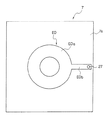
以下、図面を参照して本発明の実施の形態を詳細に説明する。図1は、本発明の実施の形態の加速度センサ素子を組み込んだ三軸加速度センサの概略断面図であり、図2は図1の部分拡大図である。本図に示すように、この三軸加速度センサは、ダイアフラム1と、重錘3と、ベース5と、ダイアフラム1の重錘3が取り付けられた面側とは反対側の面上に固定された加速度センサ素子7とを備えている。なお、本図では、理解を容易にするため、加速度センサ素子7の主要部の厚みを誇張して描いている。これらの各部材は、枠状の絶縁樹脂製ケース9内に収納されている。そして、絶縁樹脂製ケース9には、樹脂成形体21に加速度センサ素子7の出力電極OX,OY,OZ及び電極OD,OE,OD(図3参照)にそれぞれ接続される3本の端子金具25…が固定されてなる2つの端子ユニット11,11が嵌合されている。またケース9の上側開口部には、金属製の蓋部材6が取り付けられている。
【0011】
ダイアフラム1,重錘3及びベース5は、真鍮からなる金属材料により一体に成形された単体ユニット10として構成されている。ダイアフラム1は、円板形状を有している。重錘3は、円柱形状を有しており、その中心線の延長部分がダイアフラム1の中心を通るようにダイアフラム1と一体化されている。ベース5は円筒形状を有しており、ダイアフラム1の外周部を支持している。絶縁樹脂製ケース9は、単体ユニット10をインサートとして一体にインサート成形されており、ベース5の外周部には、単体ユニット10の絶縁樹脂製ケース9からの抜け止めを図るV字溝5aがベース5の周方向に連続して形成されている。
【0012】
この例では、加速度センサ素子7として、図3の平面図及び図4の裏面図に示すように圧電セラミックス基板7aの表面に三軸加速度検出用の加速度検出用電極パターンE1 が形成され、裏面に対向電極パターンE0 が形成されて構成された圧電型三軸加速度センサ素子を用いている。
【0013】
圧電セラミックス基板7aの裏面及び対向電極パターンE0 は、エポキシ等の合成樹脂材料からなる接着剤層4によってダイアフラム1の表面に接合されている。圧電セラミックス基板7aは、輪郭形状が四角形をなしており、内部に応力が加わると自発分極電荷が発生するように電極に対応した部分に分極処理が施されている。分極処理については後に説明する。図3に示すように、圧電セラミックス基板7aは、重錘対向領域8Aと、ベース対向領域8Bと、重錘対向領域8Aとベース対向領域8Bとの間に位置する中間領域8Cとを有している。重錘対向領域8Aに対応する部分には重錘3が位置しており、ベース対向領域8Bに対応する部分にはベース5が位置している。中間領域8Cは、重錘対向領域8Aを囲む第1の応力発生領域8C1と、第1の応力発生領域8C1とベース対向領域8Bとの間に位置する第2の応力発生領域8C2とから構成されている。第1の応力発生領域8C1は、重錘3に加速度が作用したときに変形して内部に応力が発生する領域であり、表面側に加速度検出用電極パターンE1の加速度検出用電極EX1〜EZ4が形成されている。この第1の応力発生領域8C1は、重錘3に対して圧電セラミックス基板7aの基板面と平行な方向(X軸方向またはY軸方向)に加速度が作用すると、重錘3の重心を中心として点対称に異なった状態(引っ張り応力が加わった状態と、圧縮応力が加わった状態と)に変形する。また、重錘3に対して圧電セラミックス基板7aの基板面と直交する方向(Z軸方向)に加速度が作用すると、第1の応力発生領域8C1の各部は同じ状態に変形する。第2の応力発生領域8C2は、第1の応力発生領域8C1に比べて僅かな応力しか発生しない領域である。なお、図3において、8Dは第1の応力発生領域8C1と第2の応力発生領域8C2との境界線(中立線)である。
【0014】
圧電セラミックス基板7aの表面及び裏面に形成された加速度検出用電極パターンE1及び対向電極パターンE0はいずれもスクリーン印刷により形成されている。加速度検出用電極パターンE1 は、図3に示すように、X軸方向検知電極パターン13とY軸方向検知電極パターン15とZ軸方向検知電極パターン17とを有している。X軸方向検知電極パターン13は、一対のX軸方向加速度検出用電極EX1,EX2とX軸出力電極OXとが接続線L1,L2により直列に接続された構造を有している。一対のX軸方向加速度検出用電極EX1,EX2は、後に説明するY軸方向検知電極パターン15の一対のY軸方向加速度検出用電極EY1,EY2及びZ軸方向検知電極パターン17の4つのZ軸方向加速度検出用電極EZ1〜EZ4と共に、重錘対向領域8Aを囲む環状の列を形成している。一対のX軸方向加速度検出用電極のそれぞれの電極EX1,EX2は、X軸方向仮想線XLに対して線対称になり且つ重錘対向領域8Aと第1の応力発生領域8C1とに跨がる矩形に近い形状を有している。X軸出力電極OXはほぼ正方形の形状を有しており、第2の応力発生領域8C2の外側にある圧電セラミックス基板7aの外周縁部に位置するように形成されている。
【0015】
Y軸方向加速度検出用電極パターン15は、一対のY軸方向加速度検出用電極EY1,EY2とY軸出力電極OYとが接続線L3〜L5により直列に接続された構造を有している。一対のY軸方向加速度検出用電極のそれぞれの電極EY1,EY2もX軸方向加速度検出用電極EX1及びEX2と同様な形状を有しており、Y軸方向仮想線YLに対して線対称になり且つ重錘対向領域8Aと第1の応力発生領域8C1とに跨がる矩形に近い形状を有している。Y軸出力電極OYはX軸出力電極OXと同様にほぼ正方形の形状を有しており、第2の応力発生領域8C2の外側にある圧電セラミックス基板7aの外周縁部に位置するようにX軸出力電極OXと並んで形成されている。
【0016】
Z軸方向加速度検出用電極パターン17は、Z軸方向加速度検出用電極EZ1〜EZ4及びZ軸出力電極OZが、これらの順に接続線L6〜L9によって直列に接続された構造を有している。4つのZ軸方向加速度検出用電極EZ1〜EZ4は、それぞれ一対のX軸方向加速度検出用電極EX1,EX2及び一対のY軸方向加速度検出用電極EY1,EY2の各電極の間に配置されるように形成されている。Z軸方向加速度検出用電極EZ1〜EZ4の各電極は、矩形に近い形状を有しており、X軸方向加速度検出用電極EX1及びEX2と同様に重錘対向領域8Aと第1の応力発生領域8C1とに跨がって形成されている。Z軸出力電極OZもX軸出力電極OXと同様にほぼ正方形の形状を有しており、第2の応力発生領域8C2の外側にある圧電セラミックス基板7aの外周縁部に位置するようにX軸出力電極OX及びY軸出力電極OYと並んで形成されている。
【0017】
出力電極OX,OY,OZが並ぶセラミックス基板7aの辺と対向する辺に沿う部分には、3つの電極OD,OE,ODが出力電極OX,OY,OZと平行をなすように並んで形成されている。電極OEは、アース端子に接続されるアース電極を構成しており、2つの電極OD,ODは、支持用ダミー端子を接続するためだけのダミー電極を構成している。
【0018】
圧電セラミックス基板7aの裏面上に形成された対向電極パターンE0 は、図4に示すように、加速度検出用電極パターンE1の加速度検出用電極EX1〜EZ4と対向する円環状の対向電極E0aと、対向電極E0aから圧電セラミックス基板7aの縁部に延びる延伸部E0bとを有している。延伸部E0bは、その端部が加速度検出用電極パターンE1 のアース電極OEと対向しており、図2に示すように、圧電セラミックス基板7aを貫通するスルーホール29の内壁を覆う接続部OE1及びスルーホール導電部27を介してアース電極OEと電気的に接続されている。これにより、アース電極OEと対向電極パターンE0に含まれる対向電極E0aとがスルーホール導電部27を介して電気的に接続されることになる。スルーホール導電部27は、スルーホール29と各電極OE,E0とを貫通する貫通孔39に樹脂銀が充填されて形成されており、アース電極OE及び延伸部E0bの各表面に両端部が露出している。また、アース電極OEは、圧電セラミックス基板7aの側部を通る導電性接着剤層31を介して単体ユニット10とも電気的に接続されている。これにより、対向電極E0aと単体ユニット10の双方がアース電極OEと電気的に接続されることになる。
【0019】
図3に戻って、X軸方向加速度検出用電極EX1,EX2に対応する圧電セラミックス基板7aの各部分には、重錘3にZ軸方向(図3の紙面と直交する方向)の加速度が作用して各部分に同種類の応力が発生したときに重錘対向領域8Aの一方の側に位置する加速度検出用電極EX1と他方の側に位置する加速度検出用電極EX2とにそれぞれ逆極性の自発分極電荷が現れるように分極処理が施されている。また、Y軸方向加速度検出用電極EY1,EY2に対応する圧電セラミックス基板7aの各部分もX軸方向加速度検出用電極EX1,EX2に対応する圧電セラミックス基板7aの各部分と同様に、重錘3にZ軸方向の加速度が作用して各部分に同種類の応力が発生したときに重錘対向領域8Aの一方の側に位置するY軸方向加速度検出用電極EY1と他方の側に位置するY軸方向加速度検出用電極EY2とにそれぞれ逆極性の自発分極電荷が現れるように分極処理が施されている。また、Z軸方向加速度検出用電極EZ1〜EZ4に対応する圧電セラミックス基板7aの各部分は、重錘3にZ軸方向の加速度が作用して各部分に同種類の応力が発生したときにすべてのZ軸方向加速度検出用電極EZ1〜EZ4に同じ極性の自発分極電荷が現れるように分極処理が施されている。このため、重錘3に作用する加速度に基づいてダイアフラム1が変形すると圧電セラミックス基板7aが撓んで加速度検出用電極パターンE1 と対向電極パターンE0 との間に発生する自発分極電荷が変化して、重錘3に加わった三軸(X軸,Y軸,Z軸)方向の加速度が電流または電圧の変化として測定される。
【0020】
次に本実施の形態の加速度センサ素子の製造方法について説明する。まず、図5(A)に示すように、スルーホール29を備えた圧電セラミックス基板7aを用意する。この圧電セラミックス基板7aは、グリーンシート状態のセラミックス基板にパンチングを用いてスルーホール29を形成した後にセラミックス基板を焼成して形成した。次に、図5(B)に示すように、圧電セラミックス基板7aの表面にガラス−銀からなる導電性塗料を塗布した後これを予備乾燥して、加速度検出用電極EX1〜EZ4と電極OX〜OZ,OD,OE,ODを印刷形成する。この時、アース電極OEを形成する導電性塗料は、スルーホール29の内壁を通して圧電セラミックス基板7aの裏面側に流れ出し、スルーホール29の内壁及び圧電セラミックス基板7aの裏面上には、接続部OE1が形成される。次に、図5(C)に示すように、圧電セラミックス基板7aの裏面にガラス−銀からなる導電性塗料を塗布した後これを予備乾燥して、対向電極パターンE0を印刷形成する。次に、加速度検出用電極EX1〜EZ4、電極OX〜OZ,OD,OE,OD及び対向電極パターンE0を焼成する。次に加速度検出用電極EX1〜EZ4及び対向電極パターンE0の対向電極E0aの対向する各電極間に直流電圧を印加することにより圧電セラミックス基板7aの所定位置に分極処理を施す。次に接続部OE1の内壁に囲まれた貫通孔39に樹脂−銀塗料からなる導電性塗料を充填すると共に同材料の導電性塗料を圧電セラミックス基板7aの表面に塗布してから加熱硬化して、接続線L1〜L9からなる接続パターンと図5(D)に示すようなスルーホール導電部27を印刷形成する。このような方法で加速度センサ素子を製造すれば、スルーホール導電部を形成する工程と接続パターンL1〜L9を形成する工程とを同じ導電性塗料を用いて同時に実施することができるので、後述の図6に示す電極を印刷形成する前にスルーホール導電部を形成する方法に比べて印刷形成の工程を一つ少なくすることができる。また、この方法で製造した加速度センサ素子は、加速度センサ素子とダイアフラムとを接合した後においても、加速度センサ素子の表面側からスルーホール導電部が形成されているか否かを目視により確認できる利点がある。
【0021】
図6(A)〜(C)は、他の方法で加速度センサ素子を製造する態様を示している。この方法では、電極を印刷形成する前にスルーホール導電部を形成しており、次の様にして実施する。まず、図6(A)に示すように、厚み方向に貫通するスルーホール29を備えた圧電セラミックス基板7aを用意する。次にスルーホール29に樹脂−銀塗料からなる導電性塗料を充填してから加熱硬化して図6(B)に示すようなスルーホール導電部37を形成する。次に、図6(C)に示すように、圧電セラミックス基板7aの表面及び裏面にそれぞれガラス−銀からなる導電性塗料を塗布した後に焼成して、圧電セラミックス基板7aの表面に加速度検出用電極EX1〜EZ4と電極OX〜OZ,OD,OE’,ODを印刷形成し、圧電セラミックス基板7aの裏面に対向電極パターンE0’を印刷形成する。これにより、アース電極OE’と対向電極パターンE0’の延伸部E0b’とがスルーホール導電部37を介して電気的に接続される。次に加速度検出用電極EX1〜EZ4及び対向電極パターンE0’の対向電極E0a’の対向する各電極間に直流電圧を印加することにより圧電セラミックス基板7aの所定位置に分極処理を施す。次に樹脂−銀塗料からなる導電性塗料を圧電セラミックス基板7aの表面に塗布してから加熱硬化して接続線L1〜L9からなる接続パターンを印刷形成して加速度センサ素子を完成する。このようにして加速度センサ素子7を製造すれば、圧電セラミックス基板7aの両面に位置するスルーホール導電部37の両端部を覆うようにアース電極OE’と対向電極パターンE0’とが形成されるので、アース電極OE’及び対向電極パターンE0’の表面を平滑にできる。
【0022】
【発明の効果】
本発明によれば、スルーホール導電部を用いてアース電極と対向電極とを電気的に接続するので、従来のように非導電物が混ることなく、アース電極と対向電極との導電部を形成することができる。そのため、対向電極とアース電極との導通を確実に図ることができる。また、従来のように、接着剤層中に導電接続部を形成する必要がないので、対向電極とダイアフラムとは、接着剤層のみで接合される。そのため、温度変化によって接着剤層に歪が生じることはなく、加速度センサ素子の検出精度が低下するのを防ぐことができる。
【図面の簡単な説明】
【図1】本発明の実施の形態の加速度センサ素子を組み込んだ三軸加速度センサの概略断面図である。
【図2】図1の部分拡大図である。
【図3】本発明の実施の形態の加速度センサ素子の平面図である。
【図4】本発明の実施の形態の加速度センサ素子の裏面図である。
【図5】(A)〜(D)は、本発明の実施の形態の加速度センサ素子の製造方法を説明するために用いる図である。
【図6】(A)〜(C)は、本発明の他の実施の形態の加速度センサ素子の製造方法を説明するために用いる図である。
【符号の説明】
7 加速度センサ素子
27 スルーホール導電部
EX1〜EZ4 加速度検出用電極
OE アース電極
E0 対向電極パターン
E0a 対向電極
E0b 延伸部[0001]
BACKGROUND OF THE INVENTION
The present invention relates to an acceleration sensor element used in an acceleration detection device that detects acceleration in a predetermined direction and a method for manufacturing the same.
[0002]
[Prior art]
A metal diaphragm with a weight in the center, a metal base that supports the outer periphery of the diaphragm, and an adhesive layer on the surface opposite to the surface on which the diaphragm weight is provided There is known an acceleration detection device including an acceleration sensor element fixed via the interface. The acceleration sensor element used here has an acceleration detection electrode and one or more electrodes including a ground electrode formed on one surface of a piezoelectric ceramic substrate, and a counter electrode facing the acceleration detection electrode on the other surface. And outputs an acceleration signal corresponding to the deformation of the diaphragm based on the acceleration acting on the weight. In such an acceleration sensor element, the counter electrode is usually electrically connected to the ground electrode. Conventionally, a conductive connecting portion made of silver paint or the like connected to both is formed in the adhesive layer between the counter electrode and the diaphragm, and a conductive portion made of conductive adhesive or the like is connected between the diaphragm and the ground electrode. And the counter electrode and the ground electrode were electrically connected.
[0003]
[Problems to be solved by the invention]
However, when a conductive connection portion made of a silver paint is formed in the adhesive layer, the adhesive of the adhesive layer and the silver paint are mixed and the conductivity of the conductive connection portion is lowered. Moreover, since the thermal expansion coefficient differs between the adhesive layer and the conductive connection portion, the adhesive layer may be distorted due to a temperature change and the detection accuracy of the acceleration sensor element may be reduced.
[0004]
An object of the present invention is to provide an acceleration sensor element and a method for manufacturing the acceleration sensor element that can reliably establish conduction between a counter electrode and a ground electrode.
[0005]
Another object of the present invention is to provide an acceleration sensor element that can prevent the detection accuracy of the acceleration sensor from being lowered due to a temperature change, and a method for manufacturing the same.
[0006]
[Means for Solving the Problems]
In the present invention, an acceleration detection electrode and one or more electrodes including a ground electrode are formed on one surface of a piezoelectric ceramic substrate, and a counter electrode facing the acceleration detection electrode is formed on the other surface. The acceleration sensor element is an object of improvement.
[0007]
In the present invention, the ground electrode and the counter electrode are electrically connected through a through-hole conductive portion that penetrates the piezoelectric ceramic substrate. If the ground electrode and the counter electrode are electrically connected using the through-hole conductive portion as in the present invention, the conductive portion between the ground electrode and the counter electrode can be reduced without mixing non-conductive materials as in the prior art. Can be formed. Therefore, electrical conduction between the counter electrode and the ground electrode can be ensured. Further, unlike the prior art, since it is not necessary to form a conductive connection portion in the adhesive layer, the counter electrode and the diaphragm are joined only by the adhesive layer. Therefore, the adhesive layer is not distorted due to a temperature change, and the detection accuracy of the acceleration sensor element can be prevented from being lowered.
[0008]
The acceleration sensor element of the present invention includes a piezoelectric ceramic substrate forming step for forming a piezoelectric ceramic substrate having a through-hole penetrating in the thickness direction, and acceleration detection on the surface using conductive paint on the front and back surfaces of the piezoelectric ceramic substrate, respectively. Forming an electrode for printing and one or more electrodes and forming a counter electrode on the back surface, a polarization process for applying a polarization treatment between the acceleration detection electrode and the counter electrode, and conducting through holes A through-hole conductive part forming step of filling the paint to form a through-hole conductive part and electrically connecting the ground electrode and the counter electrode via the through-hole conductive part; and a conductive paint on the surface of the piezoelectric ceramic substrate And forming a connection pattern connected to the acceleration detecting electrode by printing, and forming a through-hole conductive part And it can be prepared by the method carried out simultaneously using the same conductive paint connection pattern forming step. By manufacturing the acceleration sensor element in this way, the through-hole conductive portion forming step and the connection pattern forming step can be simultaneously performed using the same conductive paint. One print forming process can be reduced compared with the method of printing and forming an electrode. Further, in the conventional acceleration sensor element in which the conductive connection portion is formed in the adhesive layer, it cannot be visually confirmed whether or not the conductive connection portion is formed after the acceleration sensor element and the diaphragm are joined. . On the other hand, the acceleration sensor element manufactured by this method can visually confirm whether or not a through-hole conductive portion is formed from the surface side of the acceleration sensor element even after the acceleration sensor element and the diaphragm are joined. There are advantages.
[0009]
Further, the through-hole conductive portion may be formed before each electrode is printed. In this case, after each electrode is printed and formed, a polarization process is performed between the acceleration detection electrode and the counter electrode. If the acceleration sensor element is manufactured in this way, the ground electrode and the counter electrode are formed so as to cover both end portions of the through-hole conductive portion located on both sides of the piezoelectric ceramic substrate. Can be smoothed.
[0010]
DETAILED DESCRIPTION OF THE INVENTION
Hereinafter, embodiments of the present invention will be described in detail with reference to the drawings. FIG. 1 is a schematic sectional view of a triaxial acceleration sensor incorporating an acceleration sensor element according to an embodiment of the present invention, and FIG. 2 is a partially enlarged view of FIG. As shown in this figure, this triaxial acceleration sensor is fixed on a surface opposite to the surface of the diaphragm 1, the weight 3, the base 5, and the surface of the diaphragm 1 on which the weight 3 is attached. And an
[0011]
The diaphragm 1, the weight 3 and the base 5 are configured as a
[0012]
In this example, as the
[0013]
The back surface of the piezoelectric
[0014]
Both the acceleration detection electrode pattern E1 and the counter electrode pattern E0 formed on the front and back surfaces of the piezoelectric
[0015]
The Y-axis direction acceleration
[0016]
The Z-axis direction acceleration
[0017]
Three electrodes OD, OE, and OD are formed side by side so as to be parallel to the output electrodes OX, OY, and OZ at a portion along the side facing the side of the
[0018]
As shown in FIG. 4, the counter electrode pattern E0 formed on the back surface of the piezoelectric
[0019]
Returning to FIG. 3, acceleration in the Z-axis direction (direction perpendicular to the paper surface of FIG. 3) acts on the weight 3 on each part of the piezoelectric
[0020]
Next, a method for manufacturing the acceleration sensor element of the present embodiment will be described. First, as shown in FIG. 5A, a piezoelectric
[0021]
FIGS. 6A to 6C show a mode in which the acceleration sensor element is manufactured by another method. In this method, the through-hole conductive portion is formed before the electrode is printed and is performed as follows. First, as shown in FIG. 6A, a piezoelectric
[0022]
【Effect of the invention】
According to the present invention, since the ground electrode and the counter electrode are electrically connected using the through-hole conductive portion, the conductive portion between the ground electrode and the counter electrode is not mixed with a non-conductive material as in the prior art. Can be formed. Therefore, electrical conduction between the counter electrode and the ground electrode can be ensured. Further, unlike the prior art, since it is not necessary to form a conductive connection portion in the adhesive layer, the counter electrode and the diaphragm are joined only by the adhesive layer. Therefore, the adhesive layer is not distorted due to a temperature change, and the detection accuracy of the acceleration sensor element can be prevented from being lowered.
[Brief description of the drawings]
FIG. 1 is a schematic sectional view of a triaxial acceleration sensor incorporating an acceleration sensor element according to an embodiment of the present invention.
FIG. 2 is a partially enlarged view of FIG.
FIG. 3 is a plan view of the acceleration sensor element according to the embodiment of the present invention.
FIG. 4 is a rear view of the acceleration sensor element according to the embodiment of the present invention.
FIGS. 5A to 5D are diagrams used for explaining a method of manufacturing an acceleration sensor element according to an embodiment of the present invention. FIGS.
FIGS. 6A to 6C are views used for explaining a method of manufacturing an acceleration sensor element according to another embodiment of the present invention. FIGS.
[Explanation of symbols]
7
Claims (1)
厚み方向に貫通するスルーホールを備えた圧電セラミックス基板を形成する圧電セラミックス基板形成工程と、
前記スルーホールに導電性塗料を充填してスルーホール導電部を形成するスルーホール導電部形成工程と、
ガラス−銀からなる電極形成用の導電性塗料を用いて前記圧電セラミックス基板の表面に前記加速度検出用電極と前記アース電極を含む1以上の電極を印刷形成するとともに、前記スルーホールの内壁を通して前記圧電セラミックス基板の裏面側に流れ出した前記電極形成用の導電性塗料により前記スールーホールの内壁を覆う接続部を形成し、前記圧電セラミックス基板の裏面に前記対向電極を印刷形成する電極形成工程と、
前記加速度検出用電極と前記対向電極との間に分極処理を施す分極処理工程と、
前記スルーホールにスルーホール導電部形成用の導電性塗料を充填してスルーホール導電部を形成して、前記アース電極と前記対向電極とを前記スルーホール導電部を介して電気的に接続するスルーホール導電部形成工程と、
前記圧電セラミックス基板の前記表面にパターン形成用の導電性塗料を塗布して前記加速度検出用電極に接続される接続パターンを印刷形成する接続パターン形成工程とを具備し、
前記スルーホール導電部形成工程及び前記接続パターン形成工程は、前記スルーホール導電部形成用の導電性塗料及び前記パターン形成用の導電性塗料として樹脂−銀塗料からなる同じ導電性塗料を用いて同時に実施することを特徴とする加速度センサ素子の製造方法。An acceleration sensor element in which an acceleration detection electrode and one or more electrodes including a ground electrode are formed on one surface of a piezoelectric ceramic substrate, and a counter electrode facing the acceleration detection electrode is formed on the other surface. A manufacturing method of
A piezoelectric ceramic substrate forming step of forming a piezoelectric ceramic substrate having a through hole penetrating in the thickness direction;
A through hole conductive part forming step of forming a through hole conductive part by filling the through hole with a conductive paint;
One or more electrodes including the acceleration detecting electrode and the ground electrode are printed on the surface of the piezoelectric ceramic substrate using a conductive paint for forming an electrode made of glass-silver , and the through hole is formed through the inner wall of the through hole. An electrode forming step of forming a connection portion that covers an inner wall of the through hole with the electrode-forming conductive paint that has flowed out to the back side of the piezoelectric ceramic substrate, and printing the counter electrode on the back surface of the piezoelectric ceramic substrate;
A polarization treatment step of performing a polarization treatment between the acceleration detection electrode and the counter electrode;
A through hole is formed by filling the through hole with a conductive paint for forming a through hole conductive portion to form a through hole conductive portion, and electrically connecting the ground electrode and the counter electrode through the through hole conductive portion. Hall conductive part forming step,
A connection pattern forming step of applying a pattern-forming conductive paint on the surface of the piezoelectric ceramic substrate and printing a connection pattern connected to the acceleration detection electrode; and
The through-hole conductive part forming step and the connection pattern forming step are performed simultaneously using the conductive paint for forming the through-hole conductive part and the same conductive paint made of resin-silver paint as the conductive paint for pattern formation. A method of manufacturing an acceleration sensor element, characterized in that:
Priority Applications (1)
| Application Number | Priority Date | Filing Date | Title |
|---|---|---|---|
| JP26419999A JP4864183B2 (en) | 1999-09-17 | 1999-09-17 | Method for manufacturing acceleration sensor element |
Applications Claiming Priority (1)
| Application Number | Priority Date | Filing Date | Title |
|---|---|---|---|
| JP26419999A JP4864183B2 (en) | 1999-09-17 | 1999-09-17 | Method for manufacturing acceleration sensor element |
Publications (2)
| Publication Number | Publication Date |
|---|---|
| JP2001091532A JP2001091532A (en) | 2001-04-06 |
| JP4864183B2 true JP4864183B2 (en) | 2012-02-01 |
Family
ID=17399871
Family Applications (1)
| Application Number | Title | Priority Date | Filing Date |
|---|---|---|---|
| JP26419999A Expired - Fee Related JP4864183B2 (en) | 1999-09-17 | 1999-09-17 | Method for manufacturing acceleration sensor element |
Country Status (1)
| Country | Link |
|---|---|
| JP (1) | JP4864183B2 (en) |
-
1999
- 1999-09-17 JP JP26419999A patent/JP4864183B2/en not_active Expired - Fee Related
Also Published As
| Publication number | Publication date |
|---|---|
| JP2001091532A (en) | 2001-04-06 |
Similar Documents
| Publication | Publication Date | Title |
|---|---|---|
| US5050035A (en) | Capacitive pressure sensor and method of manufacturing same | |
| EP0164316B1 (en) | Electrical inclination sensor and method for its manufacture | |
| SE506558C2 (en) | Sensor element for pressure transducer | |
| JP2011519032A (en) | Sensing element assembly and method | |
| KR100621269B1 (en) | Strain-sensitive resistor | |
| CN105784217B (en) | Sensor module and method for manufacturing sensor module | |
| US6439056B1 (en) | Sensor element having temperature measuring means | |
| KR960024379A (en) | Mounting Structure of Acceleration Detection Element | |
| JP4864183B2 (en) | Method for manufacturing acceleration sensor element | |
| JP2005315847A (en) | Acceleration sensor | |
| US7066030B2 (en) | Pressure-measuring configuration, with a throughplating through a separator located between a diaphragm and a base, as well as a process for providing the electrical contact | |
| US7942055B2 (en) | Acceleration sensor | |
| JPH10300609A (en) | Electrostatic capacitance type pressure sensor | |
| JP3684658B2 (en) | Magnetoresistive element and manufacturing method thereof | |
| JP4286407B2 (en) | Piezoelectric three-axis acceleration sensor | |
| JP4275269B2 (en) | Piezoelectric three-axis acceleration sensor | |
| JP4156111B2 (en) | Acceleration detector | |
| JP4093646B2 (en) | Acceleration detector | |
| JP4271447B2 (en) | Stress sensor and manufacturing method thereof | |
| JP2007171040A (en) | Physical quantity sensor | |
| JP2660517B2 (en) | Capacitive level sensor | |
| JPH02196939A (en) | Pressure sensor and its manufacture | |
| JP4365982B2 (en) | Tilt sensor | |
| JP4245747B2 (en) | Acceleration detector | |
| JPH09184774A (en) | Piezoelectric type physical quantity sensor |
Legal Events
| Date | Code | Title | Description |
|---|---|---|---|
| A621 | Written request for application examination |
Free format text: JAPANESE INTERMEDIATE CODE: A621 Effective date: 20060907 |
|
| A977 | Report on retrieval |
Free format text: JAPANESE INTERMEDIATE CODE: A971007 Effective date: 20080801 |
|
| A131 | Notification of reasons for refusal |
Free format text: JAPANESE INTERMEDIATE CODE: A131 Effective date: 20080916 |
|
| A521 | Request for written amendment filed |
Free format text: JAPANESE INTERMEDIATE CODE: A523 Effective date: 20081113 |
|
| A131 | Notification of reasons for refusal |
Free format text: JAPANESE INTERMEDIATE CODE: A131 Effective date: 20081216 |
|
| A02 | Decision of refusal |
Free format text: JAPANESE INTERMEDIATE CODE: A02 Effective date: 20090317 |
|
| A521 | Request for written amendment filed |
Free format text: JAPANESE INTERMEDIATE CODE: A523 Effective date: 20090414 |
|
| A521 | Request for written amendment filed |
Free format text: JAPANESE INTERMEDIATE CODE: A523 Effective date: 20090513 |
|
| A911 | Transfer to examiner for re-examination before appeal (zenchi) |
Free format text: JAPANESE INTERMEDIATE CODE: A911 Effective date: 20090520 |
|
| A912 | Re-examination (zenchi) completed and case transferred to appeal board |
Free format text: JAPANESE INTERMEDIATE CODE: A912 Effective date: 20090619 |
|
| A521 | Request for written amendment filed |
Free format text: JAPANESE INTERMEDIATE CODE: A523 Effective date: 20110920 |
|
| A01 | Written decision to grant a patent or to grant a registration (utility model) |
Free format text: JAPANESE INTERMEDIATE CODE: A01 |
|
| A61 | First payment of annual fees (during grant procedure) |
Free format text: JAPANESE INTERMEDIATE CODE: A61 Effective date: 20111109 |
|
| FPAY | Renewal fee payment (event date is renewal date of database) |
Free format text: PAYMENT UNTIL: 20141118 Year of fee payment: 3 |
|
| R150 | Certificate of patent or registration of utility model |
Free format text: JAPANESE INTERMEDIATE CODE: R150 |
|
| R250 | Receipt of annual fees |
Free format text: JAPANESE INTERMEDIATE CODE: R250 |
|
| R250 | Receipt of annual fees |
Free format text: JAPANESE INTERMEDIATE CODE: R250 |
|
| LAPS | Cancellation because of no payment of annual fees |