JP4856010B2 - Catalytic chemical vapor deposition system - Google Patents
Catalytic chemical vapor deposition system Download PDFInfo
- Publication number
- JP4856010B2 JP4856010B2 JP2007148306A JP2007148306A JP4856010B2 JP 4856010 B2 JP4856010 B2 JP 4856010B2 JP 2007148306 A JP2007148306 A JP 2007148306A JP 2007148306 A JP2007148306 A JP 2007148306A JP 4856010 B2 JP4856010 B2 JP 4856010B2
- Authority
- JP
- Japan
- Prior art keywords
- wire
- catalyst wire
- catalyst
- film
- vapor deposition
- Prior art date
- Legal status (The legal status is an assumption and is not a legal conclusion. Google has not performed a legal analysis and makes no representation as to the accuracy of the status listed.)
- Active
Links
Images


Description
本発明は、反応室内に設置された加熱した触媒線に原料ガスを供給し、生成した分解種を前記反応室内の被成膜基材上に堆積させて成膜を行う触媒化学気相成長装置に関する。 The present invention provides a catalytic chemical vapor deposition apparatus for forming a film by supplying a source gas to a heated catalyst wire installed in a reaction chamber and depositing the generated decomposition species on a film-forming substrate in the reaction chamber About.
触媒化学気相成長法(CAT−CVD:catalytic-Chemical Vapor Deposition)は、例えば1500〜2000℃に加熱した触媒線に反応ガス(原料ガス)を供給し、反応ガスの触媒反応もしくは熱分解反応を利用して生成した分解種(堆積種)を被成膜基材上に堆積させる成膜法である。 Catalytic Chemical Vapor Deposition (CAT-CVD), for example, supplies a reaction gas (raw material gas) to a catalyst wire heated to 1500 to 2000 ° C., and performs catalytic reaction or thermal decomposition reaction of the reaction gas. This is a film forming method in which decomposed species (deposited species) generated by use are deposited on a film forming substrate.
触媒化学気相成長法は、反応ガスの分解種を基材上に堆積させて成膜を行うという点で、プラズマCVD法と類似する。しかし、触媒化学気相成長法は、高温の触媒線上における反応ガスの触媒反応あるいは熱分解反応を利用して分解種を生成するので、プラズマを形成して反応ガスの分解種を生成するプラズマCVD法に比べて、プラズマによる表面損傷がなく、原料ガスの利用効率も高いという利点がある。 The catalytic chemical vapor deposition method is similar to the plasma CVD method in that a reactive gas decomposition species is deposited on a substrate to form a film. However, the catalytic chemical vapor deposition method uses a catalytic reaction or thermal decomposition reaction of a reaction gas on a high-temperature catalyst wire to generate decomposition species, so that plasma CVD forms a plasma and generates decomposition species of the reaction gas. Compared with the method, there are advantages that there is no surface damage due to plasma and the utilization efficiency of the source gas is high.
触媒化学気相成長法は、例えば、シリコン(Si)系の膜を成膜する際に使用されている。従来、触媒化学気相成長法に使用される触媒線には、タングステン(W)線が広く用いられている(例えば特許文献1参照)。しかし、タングステンはシリコンとの合金化反応(シリサイド化)が起こり易い。タングステンがシリサイド化すると、表面にクラックが発生して機械的強度が低下するため、触媒線の寿命が短くなる。 The catalytic chemical vapor deposition method is used, for example, when a silicon (Si) -based film is formed. Conventionally, tungsten (W) wires have been widely used as catalyst wires used in catalytic chemical vapor deposition (see, for example, Patent Document 1). However, tungsten tends to undergo an alloying reaction (silicidation) with silicon. When tungsten is silicided, cracks are generated on the surface and the mechanical strength is lowered, so that the life of the catalyst wire is shortened.
一方、タングステンに比べてシリサイド化速度の遅い材料として、タンタル(Ta)がある。このタンタル線を触媒線に用いてシリコン膜を形成する方法がある(例えば特許文献2参照)。 On the other hand, tantalum (Ta) is a material having a slower silicidation rate than tungsten. There is a method of forming a silicon film using this tantalum wire as a catalyst wire (see, for example, Patent Document 2).
しかし、タンタルはタングステンに比べて機械的強度が低く、特に、高温で使用した場合のクリープ強度が低い。このため、金属タンタルを触媒線に用いた場合、加熱時に熱伸びし、従って線径が小さくなり、線抵抗が大きくなって線温度が上昇し、溶断が起こり易くなるという問題があり、生産性の向上が図れない。 However, tantalum has a lower mechanical strength than tungsten, and in particular has a low creep strength when used at high temperatures. For this reason, when metal tantalum is used for the catalyst wire, there is a problem that the wire is thermally elongated during heating, and therefore the wire diameter is reduced, the wire resistance is increased, the wire temperature is increased, and fusing is likely to occur. Cannot be improved.
また、特許文献2には、タンタル線の表面を窒化ボロン(BN)でコーティングした触媒線が開示されているが、窒化ボロンのコーティングでタンタル触媒線の長寿命化を図るには不十分であり、更なる改善が望まれている。
本発明は上述の問題に鑑みてなされ、触媒線の長寿命化を図ることができる触媒化学気相成長装置を提供することを課題とする。 This invention is made in view of the above-mentioned problem, and makes it a subject to provide the catalytic chemical vapor deposition apparatus which can aim at the lifetime improvement of a catalyst wire.
以上の課題を解決するに当たり、本発明の触媒化学気相成長装置は、反応室内に設置された加熱した触媒線に原料ガスを供給し、生成した分解種を前記反応室内の被成膜基材上に堆積させて成膜を行う触媒化学気相成長装置であって、前記触媒線は、タンタル線の表面にそのホウ化物層が形成されてなることを特徴とする。 In solving the above-mentioned problems, the catalytic chemical vapor deposition apparatus of the present invention supplies a raw material gas to a heated catalyst wire installed in a reaction chamber and converts the generated decomposition species into a film-forming substrate in the reaction chamber. A catalytic chemical vapor deposition apparatus that deposits on top and forms a film, wherein the catalyst wire is formed by forming a boride layer on the surface of a tantalum wire.
金属タンタルのホウ化物(ホウ化タンタル)は、金属タンタルよりも硬質であるため、このホウ化物層が表面に形成されたタンタル線を触媒線として用いることで、触媒線の熱伸びを低減し、機械的強度を向上させて、長寿命化を図ることが可能となる。また、本発明によれば、タンタル線の表面に窒化ボロンやカーボンをコーティングしたものに比べて、長寿命化を図ることができる。 Since metal tantalum boride (tantalum boride) is harder than metal tantalum, by using the tantalum wire on which the boride layer is formed as the catalyst wire, the thermal elongation of the catalyst wire is reduced, It is possible to improve the mechanical strength and extend the life. In addition, according to the present invention, the life can be extended as compared with the case where boron nitride or carbon is coated on the surface of the tantalum wire.
タンタル線の表面にホウ化物層を形成する方法としては、タンタル線を反応室に設置し、反応室内にジボラン(B2H6)ガスを導入しながら、タンタル線を通電加熱する。ホウ化物層の膜厚は特に限定されず、タンタル線の加熱温度、ジボランガスのガス濃度、反応時間などにより適宜調整することができる。 As a method of forming a boride layer on the surface of the tantalum wire, the tantalum wire is placed in the reaction chamber, and the tantalum wire is energized and heated while introducing diborane (B 2 H 6 ) gas into the reaction chamber. The film thickness of the boride layer is not particularly limited, and can be appropriately adjusted depending on the heating temperature of the tantalum wire, the gas concentration of diborane gas, the reaction time, and the like.
本発明では、上記ホウ化物層が表面に形成されたタンタル線を触媒線に用い、これを通電加熱して成膜を行う。この際、触媒線の通電加熱を連続通電により行う制御手段を設置し、成膜中は触媒線の通電加熱を継続して行うことで、触媒線に対するヒートショックを和らげ、ホウ化物層のクラック発生を抑制し、触媒線の長寿命化を図ることができる。 In the present invention, the tantalum wire having the boride layer formed on the surface is used as a catalyst wire, and this is energized and heated to form a film. At this time, a control means for continuously energizing and heating the catalyst wire by continuous energization is installed, and the catalyst wire is continuously energized and heated during film formation, so that the heat shock to the catalyst wire is alleviated and cracks in the boride layer are generated. And the life of the catalyst wire can be extended.
以上述べたように、本発明の触媒化学気相成長装置によれば、触媒線の寿命を延ばして生産性の向上を図ることができる。 As described above, according to the catalytic chemical vapor deposition apparatus of the present invention, the life of the catalyst wire can be extended and the productivity can be improved.
以下、本発明の実施形態について図面を参照して説明する。 Embodiments of the present invention will be described below with reference to the drawings.
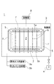
図1は本発明の実施形態による触媒化学気相成長装置の概略構成図である。触媒化学気相成長装置1は、反応室2が内部に形成された真空チャンバ3を備えている。真空チャンバ3には真空ポンプ4が接続されており、反応室2を所定の真空度に真空排気可能とされている。反応室2は、真空チャンバ3の内部に設置された防着板5の内方に形成されている。
FIG. 1 is a schematic configuration diagram of a catalytic chemical vapor deposition apparatus according to an embodiment of the present invention. The catalytic chemical
防着板5で区画された反応室2の内部には、複数本の触媒線6が設置されている。触媒線6は、タンタル(Ta)線で構成されている。本実施形態では、複数本の触媒線6が反応室2の内部を上下方向に横切るように平行に設置されている。なお、触媒線6の設置形態は上述の縦方向だけに限らず、反応室2を横方向に横切る形態で設置されていても構わない。
A plurality of
各々の触媒線6は、防着板5の天面および底面に形成された通し穴5a,5bを貫通して設置され、両端部が真空チャンバ3の外部に設置されている制御部8に接続されている。制御部8は、本発明の「制御手段」に対応し、触媒線6の通電加熱を連続通電により行うもので、電流供給源と供給電流を調整するコンピュータ等によって構成されている。
Each
反応室2の内部には、被成膜基材としての基板Sが設置されている。基板Sは、例えば矩形状のガラス基板が用いられている。本実施形態においては、図2に示すように、2枚の基板Sが触媒線6を挟むように互いに対向配置されている。ここでは、基板Sの長辺方向が触媒線6の延在方向と直交するように、基板Sが反応室2の内部に設置されている。なお、基板Sは、図示しない基板支持手段によって支持されている。この基板支持手段は、基板Sを所定温度に加熱する加熱源を内蔵した構成を有している。
Inside the
防着板5はほぼ直方形状を有しており、その4辺部にそれぞれガス導入配管7が設置されている。ガス導入配管7は、反応室2へ原料ガス又はジボラン(B2H6)ガスを導入するためのもので、ガス供給ラインを介して真空チャンバ3の外部に設置された原料ガス供給部9a及びジボランガス供給部9bに接続されている。ガス導入配管7から噴出した原料ガス又はジボランガスは、主として、2枚の基板Sの間に導入される。
The
触媒化学気相成長装置1は以上のように構成される。次に、この触媒化学気相成長装置1を用いた本実施形態の触媒化学気相成長方法について説明する。
The catalytic chemical
(第1の実施形態)
まず、真空ポンプ4を作動させて真空チャンバ3の内部を真空排気し、反応室2を所定の真空度(例えば1Pa)に減圧する。次に、ジボランガス供給部9bから反応室2へジボランガスを導入するとともに、制御部8により各触媒線6を通電し、所定温度(例えば1700℃)以上に加熱する。このとき、触媒線6の表面におけるジボランガスの接触により触媒線6の表面に反応生成物であるホウ化タンタル層が形成される。
(First embodiment)
First, the vacuum pump 4 is operated to evacuate the inside of the vacuum chamber 3, and the
上述のようにして、表面にホウ化物層が形成されたタンタル線は、金属タンタル線よりも硬質であるため、このホウ化物層が表面に形成されたタンタル線を触媒線として用いることで、触媒線6の熱伸びを低減し、機械的強度を向上させて、長寿命化を図ることができる。なお、ホウ化物層の膜厚は特に限定されず、タンタル線の加熱温度、ジボランガスのガス濃度、反応時間などにより適宜調整することができる。
Since the tantalum wire having the boride layer formed on the surface as described above is harder than the metal tantalum wire, the tantalum wire having the boride layer formed on the surface is used as a catalyst wire. The thermal elongation of the
なお、このタンタル線表面へのホウ化物層形成工程においては、真空チャンバ3の内部に基板Sを設置した後で行ってもよいし、基板Sを設置する前に行ってもよい。また、ジボランガス供給ラインを設けることができないチャンバでは、他で予めホウ化物層を形成したホウ化物タンタル触媒線を移設してきてもよい。 The boride layer forming step on the tantalum wire surface may be performed after the substrate S is installed in the vacuum chamber 3 or may be performed before the substrate S is installed. Further, in a chamber in which a diborane gas supply line cannot be provided, a boride tantalum catalyst line in which a boride layer is previously formed may be transferred.
次に、ジボランガスの導入を停止した後、原料ガス供給部9aから反応室2へ原料ガスを導入する。本実施形態では、原料ガスとしてシラン(SiH4)ガスと水素(H2)の混合ガスを用いて、基板Sの表面にシリコン(Si)膜を成膜する。なお、基板Sの表面に形成する膜は、シラン、水素、アンモニア(NH3)を用いて成膜した窒化シリコン膜(SiN)、トリシリルアミン((SiH3)3N)、アンモニア、水素を用いて成膜した窒化シリコン膜、ヘキサメチルジシラザン((CH3)3SiNHSi(CH3)3、略してHMDS)を用いて成膜した窒化シリコン膜、シラン、水素と酸素(O2)又は一酸化二窒素(N2O)を用いて成膜した酸化シリコン膜(SiO)、シランと正珪酸四エチル(Si(OC2H5)4、略してTEOS)を用いて成膜した酸化シリコン膜、シラン、水素とホスフィン(PH3)又はジボランを用いて成膜したリンドープシリコン膜(n+Si膜)やボロンドープシリコン(p+Si膜)、シラン、水素とアセチレン又はメタンを用いて成膜した炭化シリコン膜、シラン、水素、ゲルマンを用いて成膜したシリコンゲルマン膜、シラン、ヘキサフルオロプロピレンオキサイド(略してHFPO)を用いて成膜したポリテトラフルオロエチレン(登録商標「テフロン」)膜等であってもよい。なお、水素ガスを使用した水素処理を行った場合には、シリコン膜の膜中欠陥の終端や自然酸化膜除去という目的を達成できる。また、アンモニアガスを使用した窒化処理を行った場合には、シリコンの窒化を図ることができる。
Next, after the introduction of diborane gas is stopped, the source gas is introduced into the
具体的に、基板Sの成膜工程においては、制御部8により触媒線6に直流電圧を印加し、触媒線6を例えば1700℃以上の高温に加熱する。また、このとき基板Sを所定温度(例えば300℃程度)に加熱する。原料ガスは、ガス導入配管7から、互いに対向配置された2枚の基板Sの間に導入される。そして、高温に加熱された触媒線6に接触し、触媒反応もしくは熱分解反応により生成された反応ガスの分解種が基板S上に堆積して成膜される。
Specifically, in the film forming process of the substrate S, the
ここで、触媒線6の通電加熱を印加電流のオン/オフ操作で行うと、触媒線6に与えるヒートショック(加熱による伸び又は加熱解除による収縮)が大きくなるため、触媒線6の表面のクラック発生が起こり易くなり、機械的強度が低下する。そこで、本実施形態においては、基板Sの成膜時、制御部8により、触媒線6の通電加熱を継続的に行いながら触媒線6の加熱温度を制御することで、触媒線6に与えるヒートショックを低減するようにしている。
Here, if current heating of the
制御部8による触媒線の通電制御方法としては、電流量を連続的に制御して触媒線6を所定温度に加熱維持する方法のほか、触媒線6の昇降温を複数ステップで行う(ランプアップ・ダウン)方法が挙げられる。これらの方法により、触媒線6の表面に形成されているホウ化物層のクラック発生を抑制でき、機械的強度の向上を図ることができる。
As a method for controlling the energization of the catalyst wire by the
以上のように、本実施形態によれば、ホウ化物層が表面に形成されたタンタル線を触媒線6に用いることで、触媒線6の熱伸びを低減し、機械的強度の向上および長寿命化を図れるとともに、生産性の向上を図ることができる。また、触媒線がタンタルを主体とした材料で構成されているために、原料ガスとの合金化反応(シリサイド化)を抑制でき、安定した成膜を実現することができる。
As described above, according to the present embodiment, by using the tantalum wire having the boride layer formed on the surface thereof for the
また、本実施形態によれば、成膜中は触媒線6の通電加熱を継続して行うことで、触媒線に対するヒートショックを和らげ、表面ホウ化物層のクラック発生を抑制し、触媒線の長寿命化を図ることができる。図3A,Bは、表面にホウ化物層が形成された触媒線の側面SEM写真である。図3Aは、通電加熱を間欠的に(オン/オフ操作で)行ったときの例であり、表面クラックの発生が明確に現れている。また、図3Bは、通電加熱を継続的に行ったときの例であり、表面クラックの発生は認められない。
Further, according to the present embodiment, by continuously conducting the heating of the
(第2の実施形態)
次に、本発明の第2の実施形態による触媒線化学気相成長方法について説明する。
(Second Embodiment)
Next, a catalytic wire chemical vapor deposition method according to a second embodiment of the present invention will be described.
反応室2の内部に、基板Sと、触媒線6としてタンタル線を設置する。そして、真空ポンプ4を作動させて真空チャンバ3の内部を真空排気し、反応室2を所定の真空度(例えば1Pa)に減圧する。次に、原料ガス供給部9a及びジボランガス供給部9bからガス導入配管7を介して反応室2へ原料ガス及びジボランガスを導入するとともに、制御部8により各触媒線6を通電し、所定温度(例えば1700℃)以上に加熱する。
Inside the
反応室2へ導入されたジボランガスは、触媒線6と接触、分解することで、触媒線6の表面にホウ化物(ホウ化タンタル)層が形成される。これにより、触媒線6の表面が硬化することで、熱伸びが低減され、機械的強度が向上し、長寿命化が図られる。
The diborane gas introduced into the
一方、反応室2へ導入された原料ガスは、触媒線6と接触、分解することで、その反応生成物(分解種)が基板Sの表面に堆積する。これにより、基板Sの表面にシリコン膜が成膜される。なお、原料ガスの分解種であるシリコンは、ホウ素(B)よりも蒸気圧が低く、1Paの減圧雰囲気および1700℃以上の高温状態では、触媒線6に付着しない、あるいは付着してもすぐに蒸発する。従って、触媒線6の表面にはシリコン膜は堆積せず、触媒線6の表面に形成されたホウ化物層に何ら影響を及ぼさない。
On the other hand, the source gas introduced into the
なお、本実施形態においても、制御部8による触媒線6の通電加熱が継続的に行われる。これにより、触媒線6のホウ化物層形成工程および成膜工程の際における触媒線6の表層クラックの発生を抑制でき、触媒線6の機械的強度、耐久性を向上させて生産性の向上を図ることができる。
In the present embodiment, the heating of the
本実施形態によれば、上述の第1の実施形態と同様な効果を得ることができる。特に、本実施形態によれば、触媒線表面へのホウ化物層形成工程と同時に、基板Sのシリコン膜の成膜工程を実施することができるので、生産性の更なる向上を図ることができる。 According to the present embodiment, it is possible to obtain the same effect as that of the first embodiment described above. In particular, according to this embodiment, since the boride layer forming process on the surface of the catalyst wire can be performed simultaneously with the silicon film forming process of the substrate S, the productivity can be further improved. .
構成が異なる3種類の触媒線を用いてSiの成膜テストを行い、各々の触媒線の耐久性を評価した。その結果を図4に示す。図中、縦軸はモニター出力(電圧値)、横軸は積算膜厚である。すなわち、図4は、触媒線の伸びと時間との関係を示している。 A Si film formation test was performed using three types of catalyst wires having different configurations, and the durability of each catalyst wire was evaluated. The result is shown in FIG. In the figure, the vertical axis is the monitor output (voltage value), and the horizontal axis is the integrated film thickness. That is, FIG. 4 shows the relationship between the elongation of the catalyst wire and time.
実験に用いた触媒線は、コの字型に形状加工した直径1mm、長さ3000mmの金属タンタル線(純度99.5%)で構成したTa触媒線(サンプル1)、上記タンタル線表面をホウ化させたB−Ta触媒線(サンプル2)、上記タンタル線表面を窒化ボロンでコーティングしたBN−Ta触媒線(サンプル3)とした。触媒線の通電方法としては、サンプル1に関しては間欠通電(ON−OFF通電)、サンプル2に関しては連続通電および間欠通電、サンプル3に関しては連続通電とした。
The catalyst wire used in the experiment was a Ta catalyst wire (sample 1) composed of a metal tantalum wire (purity 99.5%) having a diameter of 1 mm and a length of 3000 mm processed into a U-shape. B-Ta catalyst wire (sample 2) and the above tantalum wire surface coated with boron nitride were used as the BN-Ta catalyst wire (sample 3). The energization method of the catalyst wire was intermittent energization (ON-OFF energization) for
サンプル2の初期ホウ化条件は、以下のとおりである。
[初期ホウ化条件]
ジボラン(B2H6)ガス流量:160sccm
印加電力:3kW(モニター電流値:約30A)
圧力:2Pa
The initial boriding conditions of
[Initial boriding conditions]
Diborane (B 2 H 6 ) gas flow rate: 160 sccm
Applied power: 3kW (monitor current value: about 30A)
Pressure: 2Pa
成膜テストの条件は、以下のとおりである。
[成膜テスト条件]
モノシラン(SiH4)ガス流量:32sccm
水素(H2)ガス流量:16sccm
印加電力:3kW(モニター電流値:約30A)
圧力:2Pa
The conditions for the film formation test are as follows.
[Film formation test conditions]
Monosilane (SiH 4 ) gas flow rate: 32 sccm
Hydrogen (H 2 ) gas flow rate: 16 sccm
Applied power: 3kW (monitor current value: about 30A)
Pressure: 2Pa
図4に示したように、サンプル1(Ta触媒線)は、成膜開始から急激に伸びが生じて破断に至った。伸び量は20%を超えていた。 As shown in FIG. 4, Sample 1 (Ta catalyst wire) suddenly grew from the start of film formation and reached fracture. The amount of elongation exceeded 20%.
これに対して、サンプル2(B−Ta触媒線)に関しては、サンプル1に比べて大幅に耐久性が向上した。特に、連続通電時は成膜開始から変形がほとんど認められなかった。一方、間欠通電時は、成膜開始から徐々に伸びが生じ、最終的に破断に至った。これは、電流ON−OFF時のヒートショックで表面にクラックが発生したことが原因であると考えられる。破断時の伸びは10%を越えていたが、耐久性はサンプル1に比べて5倍以上向上した。
On the other hand, the durability of Sample 2 (B-Ta catalyst wire) was significantly improved as compared to
次に、サンプル3(BN−Ta触媒線)に関しては、成膜開始から徐々に伸びが生じ、最終的に破断に至った。破断時の伸びは10%を越えていたが、耐久性はサンプル1に比べて3倍近く向上した。しかし、サンプル2の間欠通電時に比べて耐久性が劣っていた。サンプル2の間欠通電時に比べて伸びの変移が異なるのは、サンプル2に比べて表面硬度が低いからであると考えられる。
Next, with respect to Sample 3 (BN-Ta catalyst wire), elongation gradually occurred from the start of film formation, and finally, fracture occurred. Although the elongation at break exceeded 10%, the durability improved nearly three times as compared with
以上の結果から明らかなように、タンタル線の表面にホウ化物層を形成した触媒線(サンプル2)は、無垢のタンタル線(サンプル1)および窒化ボロンを表面に形成したタンタル線(サンプル3)に比べて、耐久性を大幅に向上させることができる。また、触媒線の通電加熱を連続通電とすることにより、表層クラックの発生が抑制され、触媒線の長寿命化を図れることが確認された。 As is clear from the above results, the catalyst wire (sample 2) having a boride layer formed on the surface of the tantalum wire is composed of a solid tantalum wire (sample 1) and a tantalum wire having boron nitride formed on the surface (sample 3). Compared to the above, the durability can be greatly improved. Moreover, it was confirmed that the generation of surface layer cracks was suppressed and the life of the catalyst wire could be extended by making the current heating of the catalyst wire continuous.
以上、本発明の実施形態について説明したが、本発明にこれに限定されることはなく、本発明の技術的思想に基づいて種々の変形が可能である。 The embodiment of the present invention has been described above, but the present invention is not limited to this, and various modifications can be made based on the technical idea of the present invention.
例えば以上の実施形態では、原料ガスにシランと水素の混合ガスを用いたが、原料ガスはこれに限定されず、成膜材料の種類に応じて適宜変更することが可能である。 For example, in the above embodiment, a mixed gas of silane and hydrogen is used as the source gas. However, the source gas is not limited to this, and can be appropriately changed according to the type of film forming material.
また、以上の実施形態では、反応室2の内部に2枚の基板Sを対向配置させ、これら2枚の基板の間に複数本の触媒線6を縦方向に設置した例を説明したが、反応室2の構成は上記の例に限定されない。
In the above embodiment, the example in which the two substrates S are arranged opposite to each other inside the
更に、本発明の触媒化学気相成長装置を用いて、太陽電池のP型層、N型層の成膜を行うことも可能である。
一例として、太陽電池は、まず、ガラス、アルミニウム等の基板上にMo膜などからなる金属電極をスパッタ法や熱CVD法で成膜した後、P型層(例えば、CuInSe2膜)、N型層(例えば、CdS膜)をそれぞれ成膜し、その上にZnOなどからなる透明電極を成膜することにより製造される。この例において、本装置を用いて、P型層のCuInSe2膜、N型層のCdS膜を成膜することができる。
Furthermore, it is also possible to form a P-type layer and an N-type layer of a solar cell using the catalytic chemical vapor deposition apparatus of the present invention.
As an example, in a solar cell, a metal electrode made of a Mo film or the like is first formed on a substrate such as glass or aluminum by sputtering or thermal CVD, and then a P-type layer (for example, CuInSe 2 film), N-type Each layer (for example, a CdS film) is formed, and a transparent electrode made of ZnO or the like is formed thereon. In this example, a P-type CuInSe 2 film and an N-type CdS film can be formed using this apparatus.
1 触媒化学気相成長装置
2 反応室
3 真空チャンバ
4 真空ポンプ
5 防着板
6 触媒線
7 ガス導入配管
8 制御部
9a 原料ガス供給部
9b ジボランガス供給部
DESCRIPTION OF
Claims (2)
前記触媒線は、タンタル線の表面にそのホウ化物層が形成されてなる
ことを特徴とする触媒化学気相成長装置。 A catalytic chemical vapor deposition apparatus for forming a film by supplying a source gas to a heated catalyst wire installed in a reaction chamber and depositing the generated decomposition species on a film-forming substrate in the reaction chamber,
The catalytic chemical vapor deposition apparatus, wherein the catalyst wire has a boride layer formed on a surface of a tantalum wire.
ことを特徴とする請求項1に記載の触媒化学気相成長装置。 2. The catalytic chemical vapor deposition apparatus according to claim 1, further comprising control means for performing energization heating of the catalyst wire by continuous energization.
Priority Applications (1)
| Application Number | Priority Date | Filing Date | Title |
|---|---|---|---|
| JP2007148306A JP4856010B2 (en) | 2007-06-04 | 2007-06-04 | Catalytic chemical vapor deposition system |
Applications Claiming Priority (1)
| Application Number | Priority Date | Filing Date | Title |
|---|---|---|---|
| JP2007148306A JP4856010B2 (en) | 2007-06-04 | 2007-06-04 | Catalytic chemical vapor deposition system |
Publications (2)
| Publication Number | Publication Date |
|---|---|
| JP2008300793A JP2008300793A (en) | 2008-12-11 |
| JP4856010B2 true JP4856010B2 (en) | 2012-01-18 |
Family
ID=40173980
Family Applications (1)
| Application Number | Title | Priority Date | Filing Date |
|---|---|---|---|
| JP2007148306A Active JP4856010B2 (en) | 2007-06-04 | 2007-06-04 | Catalytic chemical vapor deposition system |
Country Status (1)
| Country | Link |
|---|---|
| JP (1) | JP4856010B2 (en) |
Families Citing this family (6)
| Publication number | Priority date | Publication date | Assignee | Title |
|---|---|---|---|---|
| DE102009023471B4 (en) * | 2009-06-02 | 2012-08-30 | Fraunhofer-Gesellschaft zur Förderung der angewandten Forschung e.V. | Coating plant and process |
| JP5357689B2 (en) * | 2009-10-02 | 2013-12-04 | 三洋電機株式会社 | Catalytic CVD apparatus, film forming method, solar cell manufacturing method, and substrate holder |
| CN103415911B (en) * | 2011-03-03 | 2016-08-17 | 松下知识产权经营株式会社 | Catalytic chemical vapor film formation device, use the film build method of this device and the surface treatment method of caltalyst |
| JP5704757B2 (en) * | 2011-04-20 | 2015-04-22 | 株式会社アルバック | Electric heating wire, method for manufacturing electric heating wire, and vacuum processing apparatus |
| JP2020164932A (en) * | 2019-03-29 | 2020-10-08 | 株式会社アルバック | Electric heating wire, manufacturing method of electric heating wire, and vacuum treatment apparatus |
| JP7440346B2 (en) * | 2020-06-01 | 2024-02-28 | 株式会社アルバック | Manufacturing method and manufacturing device for energizing heating wire |
Family Cites Families (4)
| Publication number | Priority date | Publication date | Assignee | Title |
|---|---|---|---|---|
| JPS55136119A (en) * | 1979-04-09 | 1980-10-23 | Matsushita Electric Ind Co Ltd | Manufacture of boron structural material |
| JP2001358077A (en) * | 2000-06-13 | 2001-12-26 | Sharp Corp | Thin film forming device |
| JP4710187B2 (en) * | 2000-08-30 | 2011-06-29 | ソニー株式会社 | Method for growing polycrystalline silicon layer and method for epitaxial growth of single crystal silicon layer |
| JP3861178B2 (en) * | 2002-08-30 | 2006-12-20 | 広島県 | Hot filament CVD method |
-
2007
- 2007-06-04 JP JP2007148306A patent/JP4856010B2/en active Active
Also Published As
| Publication number | Publication date |
|---|---|
| JP2008300793A (en) | 2008-12-11 |
Similar Documents
| Publication | Publication Date | Title |
|---|---|---|
| US10000850B2 (en) | Deposition method and method of manufacturing a catalyst wire for a catalytic chemical vapor deposition apparatus | |
| JP4595702B2 (en) | Film forming method, film forming apparatus, and storage medium | |
| JP5919482B2 (en) | Catalytic chemical vapor deposition apparatus, film forming method using the same, and surface treatment method for catalyst body | |
| JP4856010B2 (en) | Catalytic chemical vapor deposition system | |
| WO2013141370A1 (en) | Method for manufacturing semiconductor device, method for processing substrate, substrate processing device and recording medium | |
| TW202011479A (en) | Substrate processing apparatus, plurality of electrodes and method of manufacturing semiconductor device | |
| WO2011037190A1 (en) | Deposited film formation device and deposited film formation method | |
| TW201704519A (en) | Heat generation element and method for producing same | |
| US20170211182A1 (en) | Protective layer for pecvd graphite boats | |
| KR20100037071A (en) | Heating element cvd apparatus | |
| JP2009503845A (en) | Method for passivating a substrate surface | |
| JP2020528493A (en) | Methods for depositing semiconductor films | |
| JP6667410B2 (en) | Hard mask and manufacturing method thereof | |
| TWI463030B (en) | Catalytic chemical vapor deposition device | |
| JP5635447B2 (en) | Treatment method for energized heating wire | |
| JP5704757B2 (en) | Electric heating wire, method for manufacturing electric heating wire, and vacuum processing apparatus | |
| JP5903666B2 (en) | Film forming apparatus and film forming method using the same | |
| JP2009135230A (en) | Vapor-phase-grown-film forming device and vapor-phase-grown-film forming method | |
| JP2004075493A (en) | CVD-SiC COVERED GRAPHITE MATERIAL AND ITS PRODUCTION METHOD | |
| JP5227003B2 (en) | Semiconductor device manufacturing method, substrate processing method, and substrate processing apparatus | |
| CN112921296B (en) | Method for growing graphene on special-shaped metal substrate | |
| JP2008091382A (en) | Method of forming silicon nitride film | |
| JP2013193931A (en) | Method of producing polycrystalline silicon rod | |
| CN116325179A (en) | Method for manufacturing solar cell | |
| JP2006176811A (en) | METHOD FOR PRODUCING CRYSTALLINE SiC FILM |
Legal Events
| Date | Code | Title | Description |
|---|---|---|---|
| A621 | Written request for application examination |
Free format text: JAPANESE INTERMEDIATE CODE: A621 Effective date: 20100510 |
|
| A977 | Report on retrieval |
Free format text: JAPANESE INTERMEDIATE CODE: A971007 Effective date: 20111006 |
|
| TRDD | Decision of grant or rejection written | ||
| A01 | Written decision to grant a patent or to grant a registration (utility model) |
Free format text: JAPANESE INTERMEDIATE CODE: A01 Effective date: 20111025 |
|
| A01 | Written decision to grant a patent or to grant a registration (utility model) |
Free format text: JAPANESE INTERMEDIATE CODE: A01 |
|
| A61 | First payment of annual fees (during grant procedure) |
Free format text: JAPANESE INTERMEDIATE CODE: A61 Effective date: 20111027 |
|
| FPAY | Renewal fee payment (event date is renewal date of database) |
Free format text: PAYMENT UNTIL: 20141104 Year of fee payment: 3 |
|
| R150 | Certificate of patent or registration of utility model |
Free format text: JAPANESE INTERMEDIATE CODE: R150 Ref document number: 4856010 Country of ref document: JP Free format text: JAPANESE INTERMEDIATE CODE: R150 |
|
| R250 | Receipt of annual fees |
Free format text: JAPANESE INTERMEDIATE CODE: R250 |
|
| R250 | Receipt of annual fees |
Free format text: JAPANESE INTERMEDIATE CODE: R250 |
|
| R250 | Receipt of annual fees |
Free format text: JAPANESE INTERMEDIATE CODE: R250 |
|
| R250 | Receipt of annual fees |
Free format text: JAPANESE INTERMEDIATE CODE: R250 |
|
| R250 | Receipt of annual fees |
Free format text: JAPANESE INTERMEDIATE CODE: R250 |
|
| R250 | Receipt of annual fees |
Free format text: JAPANESE INTERMEDIATE CODE: R250 |
|
| R250 | Receipt of annual fees |
Free format text: JAPANESE INTERMEDIATE CODE: R250 |
|
| R250 | Receipt of annual fees |
Free format text: JAPANESE INTERMEDIATE CODE: R250 |