JP4848876B2 - Solid-state imaging device cover and solid-state imaging device - Google Patents
Solid-state imaging device cover and solid-state imaging device Download PDFInfo
- Publication number
- JP4848876B2 JP4848876B2 JP2006204259A JP2006204259A JP4848876B2 JP 4848876 B2 JP4848876 B2 JP 4848876B2 JP 2006204259 A JP2006204259 A JP 2006204259A JP 2006204259 A JP2006204259 A JP 2006204259A JP 4848876 B2 JP4848876 B2 JP 4848876B2
- Authority
- JP
- Japan
- Prior art keywords
- solid
- layer
- imaging device
- state imaging
- image sensor
- Prior art date
- Legal status (The legal status is an assumption and is not a legal conclusion. Google has not performed a legal analysis and makes no representation as to the accuracy of the status listed.)
- Expired - Fee Related
Links
Images


Description
本発明は、固体撮像素子カバー及び固体撮像装置に関し、特に、固体撮像装置を構成するパッケージに収納された固体撮像素子を保護する固体撮像素子カバーに関する。 The present invention relates to a solid-state imaging device cover and a solid-state imaging device, and more particularly, to a solid-state imaging device cover that protects a solid-state imaging device housed in a package constituting the solid-state imaging device.
上記した固体撮像装置は、例えば、デジタルスチルカメラに用いられ、対象物の入射光を受光する固体撮像素子と、固体撮像素子を収納するパッケージと、パッケージに固定され固体撮像素子を外部(例えば、塵など)から保護する固体撮像素子カバーとを有する。固体撮像素子カバーは、例えば、特許文献1に記載のように、ガラスで構成されている。
The above-described solid-state imaging device is used in, for example, a digital still camera, and receives a solid-state imaging device that receives incident light of an object, a package that houses the solid-state imaging device, and a solid-state imaging device that is fixed to the package outside (for example, A solid-state image sensor cover that protects against dust and the like. The solid-state image sensor cover is made of glass as described in
また、固体撮像素子によって入射光を受光する際、表面反射による光量の低下を防ぐため、固体撮像素子カバーに、例えば、特許文献2に記載のような反射防止(AR:Anti-Reflection)膜が成膜される。反射防止膜は、例えば、チタン(Ti)とランタン(La)を主成分とする混合酸化物の層を有する5層構造の積層薄膜が用いられる。これらの積層薄膜は、例えば、真空加熱蒸着法を用いて成膜される。
In addition, when receiving incident light by the solid-state imaging device, an anti-reflection (AR) film as described in
詳しくは、図4に示すように、基板111側から順に、フッ化マグネシウム膜112(MgF2、屈折率n1=1.385、膜厚d1=25.8nm)、酸化アルミニウム膜113(Al2O3、屈折率n2=1.820、膜厚d2=98.0nm)、チタンとランタンの混合酸化膜114(屈折率n3=2.100、膜厚d3=121.4nm)、シリコン酸化膜115(SiO2、屈折率n4=1.480、膜厚d4=17.5nm)、フッ化マグネシウム膜116(MgF2、屈折率n5=1.385、膜厚d5=75.5nm)が成膜されている。これらの膜(反射防止膜101)の総膜厚は、338.2nmである。また、波長と反射率との関係を示す反射特性は、図5に示すグラフのようになっている。横軸は波長(nm)を示し、縦軸は反射率(%)を示す。
Specifically, as shown in FIG. 4, in order from the
しかしながら、近年、固体撮像素子カバーにガラスが用いられていることから、ガラスに含まれる重金属類からα線が発生し、このα線が固体撮像素子に悪影響を及ぼすことによって特性に劣化が生じるという問題があった。更に、反射防止膜101を構成するフッ化マグネシウム膜112,116を成膜する際、フッ化マグネシウム膜112,116の融点が低いことから(例えば、1260℃)加熱の制御が難しく、完全に気化されずに蒸発することがあり、固まった状態で基板111などに付着する場合がある。これにより、固まった状態で付着した部分に光が透過しないなどの点欠陥が発生し、外観不良が発生するという問題があった。加えて、反射防止膜101が5層構造になっており、成膜する工程数も比較的多いことから、成膜する際にゴミなどが含まれる可能性が高い。また、5層構造であり総膜厚も比較的厚いことから、膜の材料に含まれる不純物の量が多くなり、その結果、外観不良が発生するという問題があった。
However, in recent years, since glass is used for the solid-state image sensor cover, α-rays are generated from heavy metals contained in the glass, and the α-rays adversely affect the solid-state image sensor, resulting in deterioration of characteristics. There was a problem. Further, when the
本発明は、上述の如き問題を解決したものであって、固体撮像素子に与える悪影響を抑えることができ、且つ外観不良の発生を抑えることができる固体撮像素子カバー及び固体撮像装置を提供することを目的とする。 The present invention solves the problems as described above, and provides a solid-state image sensor cover and a solid-state image pickup device that can suppress the adverse effects on the solid-state image sensor and can suppress the appearance failure. With the goal.
上記課題を解決するために、本発明に係る固体撮像素子カバーは、パッケージの中に収納された固体撮像素子を保護するべく前記パッケージと固定される固体撮像素子カバーであって、前記固体撮像素子カバーは、水晶の光学軸に対して垂直にカットされてなるZカット水晶板であることを特徴とする。 In order to solve the above problems, the solid-state imaging device cover according to the present invention is a solid-state imaging device cover fixed to the package in order to protect the solid-state image pickup element housed in a package, wherein the solid-state imaging device The cover is a Z-cut quartz plate that is cut perpendicular to the optical axis of the quartz crystal .
この構成によれば、固体撮像素子カバーにZカット水晶板を用いるので、固体撮像素子カバーにガラスを用いた場合のように、ガラスに含まれる重金属類から発生するα線が固体撮像素子に悪影響を及ぼすことを防ぐことができる。これにより、固体撮像素子によって、固体撮像素子カバーを通過した入射光(光学像)を正規の状態で受光することができる。
また、更に、固体撮像素子カバーは、屈折率(ns)が1.53のZカット水晶板であるため、常光屈折率と異常光屈折率とによる複屈折は生じることがないので、入射する光を分離させることなく出射させることができる。
According to this configuration, since the Z-cut quartz plate is used for the solid-state image sensor cover, α rays generated from heavy metals contained in the glass have an adverse effect on the solid-state image sensor as in the case where glass is used for the solid-state image sensor cover. Can be prevented. Thereby, incident light (optical image) that has passed through the solid-state image sensor cover can be received in a normal state by the solid-state image sensor.
Furthermore, since the solid-state imaging device cover is a Z-cut quartz plate having a refractive index (ns) of 1.53, birefringence due to the ordinary light refractive index and the extraordinary light refractive index does not occur. Can be emitted without being separated.
本発明に係る固体撮像素子カバーでは、前記Zカット水晶板の主面上に、チタン(Ti)とランタン(La)の混合酸化膜を主成分とする層と、シリコン酸化膜(SiO 2 )を主成分とする層と、から構成された4層構造の反射防止膜が形成されていることを特徴とする。 In the solid-state imaging device cover according to the present invention, a layer mainly composed of a mixed oxide film of titanium (Ti) and lanthanum (La) and a silicon oxide film (SiO 2 ) are formed on the main surface of the Z-cut quartz plate. An antireflection film having a four-layer structure composed of a main component layer is formed .
この構成によれば、水晶板上に、チタンとランタンの混合酸化膜の層とシリコン酸化膜の層とから構成された4層構造の反射防止膜を形成するので、固体撮像素子カバーにガラスを用いた場合のように、ガラスに含まれる重金属類から発生するα線が固体撮像素子に悪影響を及ぼすことを防ぐことができるとともに、反射防止膜にフッ化マグネシウムを用いた場合のように、融点の低さに起因して点欠陥を含む外観不良になることを抑えることができる。更に、反射防止膜を4層構造にすることにより、比較的膜厚を薄くすることが可能となるとともに、成膜する工程数を少なくすることが可能となる。よって、成膜する際に反射防止膜にゴミや不純物が含まれることを抑えることが可能となり、外観不良を発生させることを抑えることができる。加えて、固体撮像素子によって、固体撮像素子カバーを通過した正規の状態に近い入射光を受光することができる。 According to this configuration, an antireflection film having a four-layer structure composed of a mixed oxide film of titanium and lanthanum and a silicon oxide film is formed on the quartz plate. As with the case where it is used, α-rays generated from heavy metals contained in the glass can be prevented from adversely affecting the solid-state imaging device, and the melting point as in the case where magnesium fluoride is used for the antireflection film. It is possible to suppress the appearance defect including point defects due to the low height. Furthermore, by making the antireflection film have a four-layer structure, the film thickness can be made relatively thin and the number of film forming steps can be reduced. Therefore, it is possible to prevent dust and impurities from being included in the antireflection film during film formation, and it is possible to suppress the appearance failure. In addition, the solid-state image sensor can receive incident light close to a normal state that has passed through the solid-state image sensor cover.
本発明に係る固体撮像素子カバーでは、前記反射防止膜は、前記Zカット水晶板側から第1層、第2層、第3層、第4層の薄膜が積層される4層構造で構成されており、前記第1層及び前記第3層は、チタン(Ti)とランタン(La)の混合酸化膜であり、前記第2層及び前記第4層は、シリコン酸化膜(SiO 2 )であることを特徴とする。
In the solid-state imaging device cover according to the present invention, the antireflection film has a four-layer structure in which thin films of a first layer, a second layer, a third layer, and a fourth layer are stacked from the Z-cut quartz plate side. The first layer and the third layer are a mixed oxide film of titanium (Ti) and lanthanum (La), and the second layer and the fourth layer are silicon oxide films (SiO 2 ). It is characterized by that .
この構成によれば、反射防止膜を構成する第1層及び第3層にチタンとランタンとの混合酸化膜を使用し、第2層及び第4層にシリコン酸化膜を使用するので、反射防止膜にフッ化マグネシウムを用いた場合のような融点の低さに起因して点欠陥を含む外観不良になることを抑えることができる。更に、4層構造にすることにより、比較的膜厚を薄くすることが可能となるとともに、成膜する工程数を少なくすることが可能となる。よって、成膜する際に反射防止膜にゴミや不純物が含まれることを抑えることが可能となり、外観不良を発生させることを抑えることができる。 According to this configuration, since the mixed oxide film of titanium and lanthanum is used for the first layer and the third layer constituting the antireflection film, and the silicon oxide film is used for the second layer and the fourth layer, the antireflection is performed. The appearance defect including point defects due to the low melting point as in the case of using magnesium fluoride for the film can be suppressed. Furthermore, by using a four-layer structure, the film thickness can be made relatively thin and the number of film forming steps can be reduced. Therefore, it is possible to prevent dust and impurities from being included in the antireflection film during film formation, and it is possible to suppress the appearance failure.
本発明に係る固体撮像素子カバーでは、前記第1層、前記第2層、前記第3層、前記第4層の屈折率及び膜厚をn1,n2,n3,n4及びd1,d2,d3,d4とするとともに、設計主波長をλ0としたときに、0.052λ0≦n1d1≦0.063λ0、0.070λ0≦n2d2≦0.085λ0、0.432λ0≦n3d3≦0.528λ0、0.200λ0≦n4d4≦0.245λ0、の関係にしたことを特徴とする。 In the solid-state imaging device cover according to the present invention, the refractive index and film thickness of the first layer, the second layer, the third layer, and the fourth layer are set to n1, n2, n3, n4 and d1, d2, d3, respectively. d4 and when the design dominant wavelength is λ0, 0.052λ0 ≦ n1d1 ≦ 0.063λ0, 0.070λ0 ≦ n2d2 ≦ 0.085λ0, 0.432λ0 ≦ n3d3 ≦ 0.528λ0, 0.200λ0 ≦ n4d4 ≦ 0.245λ0 is a characteristic.
この構成によれば、第1層〜第4層を上記のような屈折率及び膜厚にするので、可視光領域(例えば、390nm〜780nm)において低い反射率(例えば、1.0%以下)を得ることができる。その結果、固体撮像素子カバー(反射防止膜及び固体撮像素子)を介して通過した光量などの低下が抑えられた入射光を固体撮像素子によって受光することができる。 According to this configuration, since the first layer to the fourth layer have the above-described refractive index and film thickness, the reflectance is low (for example, 1.0% or less) in the visible light region (for example, 390 nm to 780 nm). Can be obtained. As a result, it is possible for the solid-state imaging device to receive incident light in which a decrease in the amount of light that has passed through the solid-state imaging device cover (antireflection film and solid-state imaging device) is suppressed.
本発明に係る固体撮像装置では、固体撮像素子カバーの主面と、前記パッケージの中に収納された前記固体撮像素子とが対向するように前記固体撮像素子カバーと前記パッケージとを固定したことを特徴とする。 In the solid-state imaging device according to the present invention, the solid-state imaging device cover and the package are fixed so that the main surface of the solid-state imaging device cover and the solid-state imaging device housed in the package face each other. Features.
この構成によれば、固体撮像素子カバーに水晶板を用いるので、固体撮像素子カバーにガラスを用いた場合のように、ガラスに含まれる重金属類から発生するα線が固体撮像素子に悪影響を及ぼすことを防ぐことができる。これにより、固体撮像素子によって、固体撮像素子カバーを通過した入射光(光学像)を正規の状態で受光することができる。 According to this configuration, since a crystal plate is used for the solid-state image sensor cover, α rays generated from heavy metals contained in the glass adversely affect the solid-state image sensor as in the case where glass is used for the solid-state image sensor cover. Can be prevented. Thereby, incident light (optical image) that has passed through the solid-state image sensor cover can be received in a normal state by the solid-state image sensor.
上記の固体撮像装置において、前記固体撮像素子カバーは、前記水晶板に成膜された、チタン(Ti)とランタン(La)の混合酸化膜を主成分とする層と、シリコン酸化膜(SiO2)を主成分とする層と、から構成された4層構造の反射防止膜を有することを特徴とする。 In the solid-state imaging device, the solid-state imaging device cover includes a layer formed mainly on a mixed oxide film of titanium (Ti) and lanthanum (La) formed on the quartz plate, and a silicon oxide film (SiO 2). And an antireflection film having a four-layer structure composed of a main component.
この構成によれば、水晶板上に、チタンとランタンの混合酸化膜の層とシリコン酸化膜の層とから構成された4層構造の反射防止膜を形成するので、固体撮像素子カバーにガラスを用いた場合のように、ガラスに含まれる重金属類から発生するα線が固体撮像素子に悪影響を及ぼすことを防ぐことができるとともに、反射防止膜にフッ化マグネシウムを用いた場合のように、融点の低さに起因して点欠陥を含む外観不良になることを抑えることができる。更に、反射防止膜を4層構造にすることにより、比較的膜厚を薄くすることが可能となるとともに、成膜する工程数を少なくすることが可能となる。よって、成膜する際に反射防止膜にゴミや不純物が含まれることを抑えることが可能となり、外観不良を発生させることを抑えることができる。加えて、固体撮像素子によって、固体撮像素子カバーを通過した正規の状態に近い入射光を受光することができる。 According to this configuration, an antireflection film having a four-layer structure composed of a mixed oxide film of titanium and lanthanum and a silicon oxide film is formed on the quartz plate. As with the case where it is used, α-rays generated from heavy metals contained in the glass can be prevented from adversely affecting the solid-state imaging device, and the melting point as in the case where magnesium fluoride is used for the antireflection film. It is possible to suppress the appearance defect including point defects due to the low height. Furthermore, by making the antireflection film have a four-layer structure, the film thickness can be made relatively thin and the number of film forming steps can be reduced. Therefore, it is possible to prevent dust and impurities from being included in the antireflection film during film formation, and it is possible to suppress the appearance failure. In addition, the solid-state image sensor can receive incident light close to a normal state that has passed through the solid-state image sensor cover.
更に、上記の固体撮像装置において、前記固体撮像素子カバーは、前記反射防止膜は、前記水晶板側から第1層、第2層、第3層、第4層の薄膜が積層される4層構造で構成されており、前記第1層及び前記第3層は、チタン(Ti)とランタン(La)の混合酸化膜であり、前記第2層及び前記第4層は、シリコン酸化膜(SiO2)であることを特徴とする。 Furthermore, in the above-described solid-state imaging device, the solid-state imaging element cover includes the anti-reflection film, the four layers in which the first layer, the second layer, the third layer, and the fourth layer are stacked from the quartz plate side. The first layer and the third layer are mixed oxide films of titanium (Ti) and lanthanum (La), and the second layer and the fourth layer are silicon oxide films (SiO 2). 2 ).
この構成によれば、反射防止膜を構成する第1層及び第3層にチタンとランタンとの混合酸化膜を使用し、第2層及び第4層にシリコン酸化膜を使用するので、反射防止膜にフッ化マグネシウムを用いた場合のような融点の低さに起因して点欠陥を含む外観不良になることを抑えることができる。更に、4層構造にすることにより、比較的膜厚を薄くすることが可能となるとともに、成膜する工程数を少なくすることが可能となる。よって、成膜する際に反射防止膜にゴミや不純物が含まれることを抑えることが可能となり、外観不良を発生させることを抑えることができる。 According to this configuration, since the mixed oxide film of titanium and lanthanum is used for the first layer and the third layer constituting the antireflection film, and the silicon oxide film is used for the second layer and the fourth layer, the antireflection is performed. The appearance defect including point defects due to the low melting point as in the case of using magnesium fluoride for the film can be suppressed. Furthermore, by using a four-layer structure, the film thickness can be made relatively thin and the number of film forming steps can be reduced. Therefore, it is possible to prevent dust and impurities from being included in the antireflection film during film formation, and it is possible to suppress the appearance failure.
また更に、上記の固体撮像装置において、前記固体撮像素子カバーでは、前記第1層、前記第2層、前記第3層、前記第4層の屈折率及び膜厚をn1,n2,n3,n4及びd1,d2,d3,d4とするとともに、設計主波長をλ0としたときに、0.052λ0≦n1d1≦0.063λ0、0.070λ0≦n2d2≦0.085λ0、0.432λ0≦n3d3≦0.528λ0、0.200λ0≦n4d4≦0.245λ0、の関係にしたことを特徴とする。 Still further, in the solid-state imaging device, in the solid-state imaging device cover, the refractive index and film thickness of the first layer, the second layer, the third layer, and the fourth layer are set to n1, n2, n3, n4. And d1, d2, d3, d4, and when the design dominant wavelength is λ0, 0.052λ0 ≦ n1d1 ≦ 0.063λ0, 0.070λ0 ≦ n2d2 ≦ 0.085λ0, 0.432λ0 ≦ n3d3 ≦ 0. 528λ0 and 0.200λ0 ≦ n4d4 ≦ 0.245λ0.
この構成によれば、第1層〜第4層を上記のような屈折率及び膜厚にするので、可視光領域(例えば、390nm〜780nm)において低い反射率(例えば、1.0%以下)を得ることができる。その結果、固体撮像素子カバー(反射防止膜及び固体撮像素子)を介して通過した光量などの低下が抑えられた入射光を固体撮像素子によって受光することができる。 According to this configuration, since the first layer to the fourth layer have the above-described refractive index and film thickness, the reflectance is low (for example, 1.0% or less) in the visible light region (for example, 390 nm to 780 nm). Can be obtained. As a result, it is possible for the solid-state imaging device to receive incident light in which a decrease in the amount of light that has passed through the solid-state imaging device cover (antireflection film and solid-state imaging device) is suppressed.
以下、本発明を具体化した実施形態について、図面を参照しながら説明する。 DESCRIPTION OF EXEMPLARY EMBODIMENTS Hereinafter, embodiments of the invention will be described with reference to the drawings.
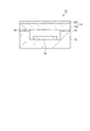
図1は、固体撮像素子カバーを有する固体撮像装置の構成を示す模式断面図である。以下、固体撮像装置の構成を、図1を参照しながら説明する。 FIG. 1 is a schematic cross-sectional view illustrating a configuration of a solid-state imaging device having a solid-state imaging element cover. Hereinafter, the configuration of the solid-state imaging device will be described with reference to FIG.
図1に示すように、固体撮像装置11は、例えばデジタルスチルカメラに用いられ、対象物の入射光を受光する固体撮像素子12と、固体撮像素子12を収納するパッケージ13と、パッケージ13に収納された固体撮像素子12を外部(例えば、塵など)から保護する固体撮像素子カバー14とを有する。
As shown in FIG. 1, the solid-
固体撮像素子12は、例えば、CCD(Charge Coupled Device)であり、入射光の光の強さに応じて蓄電容量が変化するフォトダイオードからなる光電素子(画素)をマトリクス状に配列して構成されている。この固体撮像素子12を用いて対象物を撮影すると、規則的に配列された画素上の蓄電容量が変化し、これを空間的にサンプリングすることにより、対象物に対応する電気信号を生成し、それを変換して像を構成する。このような固体撮像素子12によって、固体撮像素子カバー14を介して入射される入射光が電気信号に変換される。
The solid-
パッケージ13は、上記したように固体撮像素子12を収納し、収納された固体撮像素子12の上方が開口する凹状に形成されている。
The
固体撮像素子カバー14は、接着材料15を介して、パッケージ13の開口する領域を覆うように固定されている。また、この接着材料15によって、固体撮像素子カバー14とパッケージ13との間が密封されている。また、固体撮像素子カバー14は、カバー16と反射防止膜20とを有して構成されている。
The solid-state
図2は、固体撮像素子カバーの構成を示す模式断面図である。以下、固体撮像素子カバーの構成を、図2を参照しながら説明する。 FIG. 2 is a schematic cross-sectional view showing the configuration of the solid-state image sensor cover. Hereinafter, the configuration of the solid-state image sensor cover will be described with reference to FIG.
図2に示すように、固体撮像素子カバー14は、上記したようにカバー16と反射防止膜20とを有する。
As shown in FIG. 2, the solid-state
カバー16は、例えば、Zカット水晶板で構成されており、その主面16aが固体撮像素子12と向き合うように、パッケージ13(図1参照)に固定されている。Zカット水晶板とは、光軸に対して垂直にカットされた水晶板である。また、主面16aとは、光軸と接する面であり、一般に水晶板(カバー16)における広い面を指していう。カバー16の厚みは、例えば0.8mmである。なお、カバー16(Zカット水晶板)の屈折率(ns)は、1.53であり、複屈折(常光屈折率と異常光屈折率とによる)は生じない。
The
反射防止膜20は、4層構造で構成されており、カバー16側から順に、第1層21、第2層22、第3層23、第4層24の薄膜が積層されている。第1層21〜第4層24は、例えば、真空加熱蒸着法で成膜される。なお、設計主波長(λ0)は、580nmである。
The
第1層21は、主成分がTi(チタン)とLa(ランタン)との混合酸化物である。詳述すると、第1層21は、TiとLaとを混合したものの酸化物であり、屈折率(n1)が2.000±0.200である。また、膜厚(d1)が16.7nmであり、光学膜厚(nd1)が0.058λ0nmである。
The main component of the
第2層22は、主成分がSiO2(シリコン酸化膜)である。詳しくは、第2層22の屈折率(n2)が1.460±0.200であり、膜厚(d2)が30.8nmである。また、光学膜厚(nd2)は0.078λ0nmである。
The main component of the
第3層23は、主成分がTi(チタン)とLa(ランタン)との混合酸化膜である。詳述すると、第3層23は、第1層21と同様にTiとLaとを混合したものの酸化物であり、屈折率(n3)が2.000±0.200である。また、膜厚(d3)が139.2nmであり、光学膜厚(nd3)が0.480λ0nmである。
The
第4層24は、主成分がSiO2(シリコン酸化膜)である。詳述すると、第4層24の屈折率(n4)が1.460±0.200であり、膜厚(d4)が88.4nmである。また、光学膜厚(nd4)は0.222λ0nmである。ここで、設計主波長λ0における膜厚dと光学膜厚nd・λ0との関係は、屈折率nを用いて、n・d=nd・λ0で表すことができる。
The main component of the
以上のように、カバー16にZカット水晶板を用いることにより、従来のようなカバーにガラスを用いた場合のように、ガラスに含まれる重金属類から発生するα線によって、固体撮像素子12に悪影響を及ぼすことを防ぐことができる。
As described above, by using a Z-cut quartz plate for the
更に、第1層21(チタンとランタンの混合酸化膜)、第2層22(シリコン酸化膜)、第3層23(チタンとランタンの混合酸化膜)、第4層24(シリコン酸化膜)の4層構造で反射防止膜20を構成することにより、従来の反射防止膜にフッ化マグネシウム膜を用いた場合のように、点欠陥のような外観不良が発生することを防ぐことができる。更に、4層構造で反射防止膜20を構成することにより、総膜厚を275.1nmとすることが可能となる。よって、従来の総膜厚より薄くすることができるとともに、成膜する工程数を少なくすることができる。これにより、成膜する際に反射防止膜20の中にゴミや不純物などが含まれる量を抑えることが可能となり、外観不良が発生することを抑えることができる。
Furthermore, the first layer 21 (mixed oxide film of titanium and lanthanum), the second layer 22 (silicon oxide film), the third layer 23 (mixed oxide film of titanium and lanthanum), and the fourth layer 24 (silicon oxide film). By configuring the
図3は、反射防止膜の反射特性(波長−反射率)を示すグラフである。以下、図3を参照しながら、反射防止膜の反射特性について説明する。 FIG. 3 is a graph showing the reflection characteristics (wavelength-reflectance) of the antireflection film. Hereinafter, the reflection characteristics of the antireflection film will be described with reference to FIG.
図3に示すように、横軸は波長(nm)を示し、縦軸は反射率(%)を示す。図3に示す実線Aは本実施形態の反射防止膜20の反射特性であり、破線Bは従来の反射防止膜の反射特性である。第1層21、第2層22、第3層23、第4層24の屈折率及び膜厚をn1,n2,n3,n4及びd1,d2,d3,d4とするとともに、設計主波長をλ0としたときに、以下の式(1)〜(4)を満足していれば、可視光領域のほぼ全域(例えば、390nm〜780nm)において低い反射率(例えば、1.0%以下)を得ることができる。
(1)0.052λ0≦n1d1≦0.063λ0
(2)0.070λ0≦n2d2≦0.085λ0
(3)0.432λ0≦n3d3≦0.528λ0
(4)0.200λ0≦n4d4≦0.245λ0
As shown in FIG. 3, the horizontal axis indicates the wavelength (nm) and the vertical axis indicates the reflectance (%). The solid line A shown in FIG. 3 is the reflection characteristic of the
(1) 0.052λ0 ≦ n1d1 ≦ 0.063λ0
(2) 0.070λ0 ≦ n2d2 ≦ 0.085λ0
(3) 0.432λ0 ≦ n3d3 ≦ 0.528λ0
(4) 0.200λ0 ≦ n4d4 ≦ 0.245λ0
以上のように、従来の反射特性(破線B参照)を低下させることなく、ほぼ同様の反射特性(実線A参照)を得ることができる。また、このような構成及び特性の反射防止膜20をカバー16に形成するので、受光する入射光の品質(光量など)が固体撮像素子カバー14によって低下(劣化)することを抑えることができる。
As described above, substantially the same reflection characteristics (see the solid line A) can be obtained without degrading the conventional reflection characteristics (see the broken line B). In addition, since the
以上詳述したように、本実施形態によれば、以下に示す効果が得られる。 As described above in detail, according to the present embodiment, the following effects can be obtained.
(1)本実施形態によれば、Zカット水晶板からなるカバー16上に、チタンとランタンの混合酸化膜の層(第1層21及び第3層23)とシリコン酸化膜の層(第2層22及び第4層24)とから構成された4層構造の反射防止膜20を形成するので、カバーにガラスを用いた場合のように、ガラスに含まれる重金属類から発生するα線が固体撮像素子12に悪影響を及ぼすことを防ぐことができるとともに、反射防止膜20にフッ化マグネシウムを用いた場合のように、融点の低さに起因して点欠陥を含む外観不良になることを抑えることができる。更に、反射防止膜20を従来の5層構造から4層構造にすることにより、総膜厚を薄くすることが可能となるとともに、成膜する工程数を少なくすることが可能となる。よって、成膜する際に反射防止膜20にゴミや不純物が含まれることを抑えることが可能となり、外観不良を発生させることを抑えることができる。その結果、固体撮像素子カバー14によって、入射光の品質(例えば、光量など)が低下(劣化)することを抑えることができる。
(1) According to this embodiment, on the
(2)本実施形態によれば、反射防止膜20を構成する第1層21〜第4層24を上記のような屈折率及び膜厚にするので、従来の反射特性を低下させることなく、可視光領域(例えば、390nm〜780nm)において低い反射率(例えば、1.0%以下)を得ることができる。
(2) According to the present embodiment, since the
なお、本実施形態は上記に限定されず、以下のような形態で実施することもできる。 In addition, this embodiment is not limited above, It can also implement with the following forms.
(変形例1)上記したように、Zカット水晶板からなるカバー16に反射防止(AR)膜20を形成することに代えて、例えば、同様のカバー16に赤外線(IR)吸収膜、紫外線(UV)吸収膜、紫外線・赤外線(UVIR)吸収膜を形成するようにしてもよい。これによれば、それぞれの膜を用いた効果を得ることができるとともに、上記した効果と同様、カバーにガラスを用いた場合のようにα線によるフォトダイオードに悪影響を与えることを防ぐことができる。
(Modification 1) As described above, instead of forming the antireflection (AR)
(変形例2)上記したように、固体撮像素子12はCCDに限定されず、例えば、CMOS(Complementary Metal Oxide Semiconductor)、CPD(Charge Priming Device)などであってもよい。
(Modification 2) As described above, the solid-
(変形例3)上記したように、カバー16にZカット水晶板を用いることに限定されず、例えば、水晶板の主面の法線が水晶の光学軸であるZ軸に対して0°〜90°の範囲となるような角度でカットされた水晶板を使うようにしてもよい。水晶板のカットアングルを0°(Zカット)ではなく、例えば、45°(水晶板の主面の法線とZ軸とのなす角度)でカットしてなるカバー16を用いれば、2点分離タイプのローパスフィルターとして使用することができる。
(Modification 3) As described above, the
11…固体撮像装置、12…固体撮像装置を構成する固体撮像素子、13…固体撮像装置を構成するパッケージ、14…固体撮像装置を構成する固体撮像素子カバー、15…固体撮像装置を構成する接着材料、16…固体撮像素子カバーを構成するカバー、16a…主面、20…固体撮像素子カバーを構成する反射防止膜、21…反射防止膜を構成する第1層、22…反射防止膜を構成する第2層、23…反射防止膜を構成する第3層、24…反射防止膜を構成する第4層。
DESCRIPTION OF
Claims (5)
前記固体撮像素子カバーは、水晶の光学軸に対して垂直にカットされてなるZカット水晶板であることを特徴とする固体撮像素子カバー。 A solid-state image sensor cover fixed to the package to protect the solid-state image sensor housed in the package,
The solid-state image sensor cover is a Z-cut crystal plate cut perpendicularly to the optical axis of the crystal .
前記第1層及び前記第3層は、チタン(Ti)とランタン(La)の混合酸化膜であり、 The first layer and the third layer are a mixed oxide film of titanium (Ti) and lanthanum (La),
前記第2層及び前記第4層は、シリコン酸化膜(SiO The second layer and the fourth layer are formed of a silicon oxide film (SiO 22 )であることを特徴とする請求項2に記載の固体撮像素子カバー。The solid-state imaging device cover according to claim 2, wherein
前記第1層、前記第2層、前記第3層、前記第4層の屈折率及び膜厚をn1,n2,n3,n4及びd1,d2,d3,d4とするとともに、設計主波長をλ0としたときに、
0.052λ0≦n1d1≦0.063λ0、
0.070λ0≦n2d2≦0.085λ0、
0.432λ0≦n3d3≦0.528λ0、
0.200λ0≦n4d4≦0.245λ0、
の関係にしたことを特徴とする固体撮像素子カバー。 The solid-state image sensor cover according to claim 3,
The refractive index and film thickness of the first layer, the second layer, the third layer, and the fourth layer are n1, n2, n3, n4 and d1, d2, d3, d4, and the design dominant wavelength is λ0. And when
0.052λ0 ≦ n1d1 ≦ 0.063λ0,
0.070λ0 ≦ n2d2 ≦ 0.085λ0,
0.432λ0 ≦ n3d3 ≦ 0.528λ0,
0.200λ0 ≦ n4d4 ≦ 0.245λ0,
The solid-state image sensor cover characterized by having a relationship of
前記パッケージの中に収納された前記固体撮像素子とが対向するように前記固体撮像素子カバーと前記パッケージとを固定したことを特徴とする固体撮像装置。 The main surface of the solid-state image sensor cover according to any one of claims 1 to 4,
The solid-state imaging device, wherein the solid-state imaging device cover and the package are fixed so that the solid-state imaging device housed in the package faces each other.
Priority Applications (1)
| Application Number | Priority Date | Filing Date | Title |
|---|---|---|---|
| JP2006204259A JP4848876B2 (en) | 2006-07-27 | 2006-07-27 | Solid-state imaging device cover and solid-state imaging device |
Applications Claiming Priority (1)
| Application Number | Priority Date | Filing Date | Title |
|---|---|---|---|
| JP2006204259A JP4848876B2 (en) | 2006-07-27 | 2006-07-27 | Solid-state imaging device cover and solid-state imaging device |
Publications (3)
| Publication Number | Publication Date |
|---|---|
| JP2008034502A JP2008034502A (en) | 2008-02-14 |
| JP2008034502A5 JP2008034502A5 (en) | 2009-09-03 |
| JP4848876B2 true JP4848876B2 (en) | 2011-12-28 |
Family
ID=39123638
Family Applications (1)
| Application Number | Title | Priority Date | Filing Date |
|---|---|---|---|
| JP2006204259A Expired - Fee Related JP4848876B2 (en) | 2006-07-27 | 2006-07-27 | Solid-state imaging device cover and solid-state imaging device |
Country Status (1)
| Country | Link |
|---|---|
| JP (1) | JP4848876B2 (en) |
Families Citing this family (4)
| Publication number | Priority date | Publication date | Assignee | Title |
|---|---|---|---|---|
| JP4790874B2 (en) * | 2009-08-31 | 2011-10-12 | オリンパスメディカルシステムズ株式会社 | Imaging device |
| JP5721370B2 (en) | 2010-08-27 | 2015-05-20 | キヤノン株式会社 | Manufacturing method of optical sensor, optical sensor and camera |
| JP6056186B2 (en) * | 2012-05-08 | 2017-01-11 | 株式会社ニコン | Image sensor |
| JP2016195185A (en) * | 2015-03-31 | 2016-11-17 | キヤノン株式会社 | Manufacturing method of optical component, optical component, and optical device |
Family Cites Families (4)
| Publication number | Priority date | Publication date | Assignee | Title |
|---|---|---|---|---|
| JP2002353352A (en) * | 2001-05-30 | 2002-12-06 | Kyocera Corp | Package for storing image pickup device |
| JP2002365590A (en) * | 2001-06-06 | 2002-12-18 | Tochigi Nikon Corp | Optical element, method of manufacturing optical element and optical isolator |
| JP2004221634A (en) * | 2003-01-09 | 2004-08-05 | Seiko Epson Corp | Optical module, manufacturing method thereof, and electronic apparatus |
| JP2006084733A (en) * | 2004-09-15 | 2006-03-30 | Epson Toyocom Corp | Depolarization plate and electronic optical instrument |
-
2006
- 2006-07-27 JP JP2006204259A patent/JP4848876B2/en not_active Expired - Fee Related
Also Published As
| Publication number | Publication date |
|---|---|
| JP2008034502A (en) | 2008-02-14 |
Similar Documents
| Publication | Publication Date | Title |
|---|---|---|
| KR102061477B1 (en) | Near-infrared cut-off filter | |
| JP5013022B2 (en) | Infrared cut filter | |
| WO2014103921A1 (en) | Ir cut filter and image capture device including same | |
| KR102104081B1 (en) | Camera structure, information and communication equipment | |
| JP2007206172A (en) | Imaging system optical element | |
| CN103718070A (en) | Optical member | |
| US11101308B2 (en) | Image pickup device, image pickup apparatus, and production apparatus and method | |
| US9069126B2 (en) | Optical element, optical system and optical apparatus having antireflection coating | |
| JP2003029027A (en) | Near ir ray cut filter | |
| JP4848876B2 (en) | Solid-state imaging device cover and solid-state imaging device | |
| JP2008070828A (en) | Infrared ray shielding filter | |
| JP2006011408A (en) | Optical element and optical equipment | |
| JP4853157B2 (en) | Antireflection film, optical element, imaging device, and camera | |
| JP6174379B2 (en) | Visible light transmission filter | |
| JP2013083885A (en) | Nd filter | |
| JP2006195373A (en) | Visibility correcting near infrared cut filter, and optical low pass filter and visibility correcting element using the same | |
| JP2011081083A (en) | Neutral density (nd) filter | |
| JP5287362B2 (en) | Optical filter and imaging system | |
| JP2007304573A (en) | Near ultraviolet ray and infrared ray blocking filter, birefringent plate with near ultraviolet ray and infrared ray blocking filter, optical low pass filter and imaging apparatus | |
| US20120212809A1 (en) | Infrared Cut Filter | |
| JP2004258494A (en) | Nd filter | |
| JP2015184637A (en) | Optical element and imaging apparatus | |
| JP2003279726A (en) | Optical low pass filter with infrared blocking filter | |
| JP2012113045A (en) | Optical multilayer film, optical element, imaging assembly, digital camera and method for manufacturing optical multilayer film | |
| JP6011662B2 (en) | Imaging optical device having antireflection structure and imaging optical system having antireflection structure |
Legal Events
| Date | Code | Title | Description |
|---|---|---|---|
| A521 | Request for written amendment filed |
Free format text: JAPANESE INTERMEDIATE CODE: A523 Effective date: 20090715 |
|
| A621 | Written request for application examination |
Free format text: JAPANESE INTERMEDIATE CODE: A621 Effective date: 20090715 |
|
| A711 | Notification of change in applicant |
Free format text: JAPANESE INTERMEDIATE CODE: A712 Effective date: 20110729 |
|
| RD03 | Notification of appointment of power of attorney |
Free format text: JAPANESE INTERMEDIATE CODE: A7423 Effective date: 20110729 |
|
| A521 | Request for written amendment filed |
Free format text: JAPANESE INTERMEDIATE CODE: A523 Effective date: 20110819 |
|
| A977 | Report on retrieval |
Free format text: JAPANESE INTERMEDIATE CODE: A971007 Effective date: 20110826 |
|
| TRDD | Decision of grant or rejection written | ||
| A01 | Written decision to grant a patent or to grant a registration (utility model) |
Free format text: JAPANESE INTERMEDIATE CODE: A01 Effective date: 20110920 |
|
| A01 | Written decision to grant a patent or to grant a registration (utility model) |
Free format text: JAPANESE INTERMEDIATE CODE: A01 |
|
| A61 | First payment of annual fees (during grant procedure) |
Free format text: JAPANESE INTERMEDIATE CODE: A61 Effective date: 20111003 |
|
| R150 | Certificate of patent or registration of utility model |
Ref document number: 4848876 Country of ref document: JP Free format text: JAPANESE INTERMEDIATE CODE: R150 Free format text: JAPANESE INTERMEDIATE CODE: R150 |
|
| FPAY | Renewal fee payment (event date is renewal date of database) |
Free format text: PAYMENT UNTIL: 20141028 Year of fee payment: 3 |
|
| S531 | Written request for registration of change of domicile |
Free format text: JAPANESE INTERMEDIATE CODE: R313531 |
|
| R350 | Written notification of registration of transfer |
Free format text: JAPANESE INTERMEDIATE CODE: R350 |
|
| LAPS | Cancellation because of no payment of annual fees |