JP4837899B2 - Memory system and method - Google Patents
Memory system and method Download PDFInfo
- Publication number
- JP4837899B2 JP4837899B2 JP2004137797A JP2004137797A JP4837899B2 JP 4837899 B2 JP4837899 B2 JP 4837899B2 JP 2004137797 A JP2004137797 A JP 2004137797A JP 2004137797 A JP2004137797 A JP 2004137797A JP 4837899 B2 JP4837899 B2 JP 4837899B2
- Authority
- JP
- Japan
- Prior art keywords
- memory
- motherboard
- clock signal
- clock
- buffer
- Prior art date
- Legal status (The legal status is an assumption and is not a legal conclusion. Google has not performed a legal analysis and makes no representation as to the accuracy of the status listed.)
- Expired - Fee Related
Links
Images


Classifications
-
- G—PHYSICS
- G06—COMPUTING; CALCULATING OR COUNTING
- G06F—ELECTRIC DIGITAL DATA PROCESSING
- G06F13/00—Interconnection of, or transfer of information or other signals between, memories, input/output devices or central processing units
- G06F13/14—Handling requests for interconnection or transfer
- G06F13/16—Handling requests for interconnection or transfer for access to memory bus
- G06F13/1668—Details of memory controller
- G06F13/1673—Details of memory controller using buffers
-
- G—PHYSICS
- G06—COMPUTING; CALCULATING OR COUNTING
- G06F—ELECTRIC DIGITAL DATA PROCESSING
- G06F13/00—Interconnection of, or transfer of information or other signals between, memories, input/output devices or central processing units
- G06F13/14—Handling requests for interconnection or transfer
- G06F13/16—Handling requests for interconnection or transfer for access to memory bus
- G06F13/1668—Details of memory controller
- G06F13/1684—Details of memory controller using multiple buses
Description
本発明は、メモリシステムに係り、特にマザーボードに直接装着されるメモリシステム及び方法に関する。 The present invention relates to a memory system, and more particularly, to a memory system and method mounted directly on a motherboard.
最近、大容量のメモリを具備するメモリシステムに対する要求の増加にともなって複数のメモリチップを装着したメモリモジュールをマザーボードに連結するメモリ構造が多く使われている。例えば、SIMM(Single Inline Memory Module)またはDIMM(Dual Inline Memory Module)と呼ばれるメモリモジュールは、メイン回路やマザーボードに装着される拡張ソケットに容易に連結できるように考案された回路ボードである。 Recently, as a demand for a memory system having a large-capacity memory increases, a memory structure in which a memory module having a plurality of memory chips is connected to a mother board is often used. For example, a memory module called SIMM (Single Inline Memory Module) or DIMM (Dual Inline Memory Module) is a circuit board designed to be easily connected to an expansion socket mounted on a main circuit or a motherboard.
図1及び図2は、コンピュータシステムのメモリ構造を説明する図面である。図1及び図2を参照すれば、システム100は、メモリコントローラ104によって制御されるメモリモジュール106を具備する。メモリコントローラ104は、メモリモジュール106の読出し及び書込み動作を制御する。メモリコントローラ104は、マザーボード102に装着される。メモリコントローラ104の動作は当業者によく知られているので詳しい説明は省略する。
1 and 2 are diagrams illustrating a memory structure of a computer system. Referring to FIGS. 1 and 2, the
メモリモジュール106は、複数の連結パッド116を具備するエッジコネクタ114を含む。一般に、連結パッド116は、メモリモジュール106の両側面に配置される。複数のソケット112がマザーボード102に装着される。ソケット112は、電気的にメモリモジュール106とマザーボード102とを連結するためにエッジコネクタ114と連結される。
The
メモリモジュール106は、複数のメモリ装置108を具備する。メモリ装置108は、例えばDRAMまたはSDRAMでありうる。
The
バッファ110は、メモリコントローラ104から受信するコマンドとアドレス信号C/Aを制御する。複数のメモリ装置108とバッファ110とはメモリモジュール106に装着される。
The
図1に示した信号線は、マザーボード102とモジュール106の両方に連結される。信号線は、データバスDQ、システムクロック信号CLK、及びコマンドアドレスバスC/Aを含む。メモリ装置108は、マザーボード102に装着されている対応するソケット112を介してメモリコントローラ104から信号を受信する。
The signal line shown in FIG. 1 is connected to both the
メモリ構造において、アドレス、制御及びクロック信号線の集積度を維持することが重要である。信号反射を含む伝送ライン効果のために動作周波数が増加するほど信号線の集積度を維持し難くなる。 In the memory structure, it is important to maintain the integration of address, control and clock signal lines. As the operating frequency increases due to the transmission line effect including signal reflection, it becomes more difficult to maintain the degree of signal line integration.
伝送ライン理論によると、ソケット112を通じたマザーボード102とモジュール106との連結にはスタブ抵抗が発生する。スタブ抵抗は、信号反射及び信号集積度に悪影響を及ぼす伝送不連続現象(transmission discontinuity)を表す。
According to the transmission line theory, a stub resistance is generated in the connection between the
図1〜3において、データバスDQのような信号線302がマザーボード102上にある。信号線302は、ソケット312を介してマザーボード102上の信号線304と電気的に連結される。
1-3, a
ところが、ソケット312は、信号線302と信号線304との間に不連続部306をもたらす。不連続306は、タイミングマージンと電圧ウィンドウとを減少させ、発生したノイズを反送(reflect back)させるという問題がある。
However, the
図4において、メモリモジュール406上のスタブ抵抗416は、信号反射を減少させる。スタブ抵抗416は、メモリ読出し及び書込み動作を向上させる。しかし、スタブ抵抗416の値が増加するほど信号反射は減少するが、スタブ抵抗416による電圧降下が増加し信号電圧を減少させる。
In FIG. 4, a
信号電圧が減少すると電圧ウィンドウが減少する。そして、スタブ抵抗416は信号を遅延させるRC寄生抵抗を発生させる。
As the signal voltage decreases, the voltage window decreases. The
本発明の目的は、例えば、コマンド信号とアドレス信号とを高速で受信し高速動作が可能な構造のメモリシステムを提供することである。 An object of the present invention is to provide, for example, a memory system having a structure capable of receiving a command signal and an address signal at high speed and capable of operating at high speed.
前記技術的課題を達成するための本発明の第1実施の形態によるメモリシステムは、マザーボードに直接装着される第1バッファと、前記マザーボードに直接装着され、前記第1バッファに連結される少なくとも一つの第1メモリ装置と、前記マザーボード上において前記第1バッファ及び前記少なくとも一つの第1メモリ装置に配線される複数の信号線と、を備え、第1クロック信号線上のシステムクロック信号に応答して第2クロック信号線上の第1クロック信号を発生し、前記マザーボード上に直接装着されるクロック同期回路を備え、前記少なくとも一つの第1メモリ装置は前記第1クロック信号に同期して動作し、前記クロック同期回路は位相同期ループまたは遅延同期ループのうちいずれか一つである。
A memory system according to a first embodiment of the present invention for achieving the technical problem includes a first buffer directly attached to a motherboard, and at least one attached directly to the motherboard and coupled to the first buffer. Two first memory devices and a plurality of signal lines wired on the motherboard to the first buffer and the at least one first memory device, and in response to a system clock signal on the first clock signal line A clock synchronization circuit for generating a first clock signal on a second clock signal line and mounted directly on the motherboard; wherein the at least one first memory device operates in synchronization with the first clock signal; The clock synchronization circuit is one of a phase locked loop and a delay locked loop .
前記第1バッファは、例えば、アドレス及びコマンド信号を前記少なくとも一つの第1メモリ装置にドライビングするコマンド及びアドレスバッファである。前記コマンド及びアドレスバッファは、例えば、前記マザーボード上に配線されている第1コマンド及びアドレス信号線を介してコマンド及びアドレス信号を受信する。 The first buffer is, for example, a command and address buffer that drives address and command signals to the at least one first memory device. For example, the command and address buffer receives a command and an address signal via a first command and address signal line wired on the motherboard.
前記少なくとも一つの第1メモリ装置は、例えば、前記マザーボード上に配線されている第2コマンド及びアドレス信号線を介して前記コマンド及びアドレスバッファから前記コマンド及びアドレス信号を受信し、前記第1コマンド及びアドレス信号線は、例えば、前記第2コマンド及びアドレス信号線と垂直に配置される。 The at least one first memory device receives the command and address signal from the command and address buffer via, for example, a second command and address signal line wired on the motherboard, and receives the first command and For example, the address signal lines are arranged perpendicular to the second command and address signal lines.
前記少なくとも一つの第1メモリ装置は、例えば、DRAMまたはSDRAMである。前記少なくとも一つの第1メモリ装置は、例えば、マザーボード上に配線され、対応するデータ及びクロック信号線を介してデータ信号及びクロック信号を受信する。メモリシステムは、例えば、前記マザーボード上に装着されているソケットを通じてメモリコントローラと電気的に連結される少なくとも一つのメモリモジュールを備える。 The at least one first memory device is, for example, a DRAM or an SDRAM. The at least one first memory device is, for example, wired on a motherboard and receives a data signal and a clock signal via corresponding data and clock signal lines. For example, the memory system includes at least one memory module that is electrically connected to a memory controller through a socket mounted on the motherboard.
前記少なくとも一つのメモリモジュールは、例えば、前記少なくとも一つのメモリモジュールのモジュールボード上に装着される第2バッファと、前記少なくとも一つのメモリモジュールのモジュールボード上に装着され前記第2バッファに連結される少なくとも一つの第2メモリ装置と、を備える。 For example, the at least one memory module is connected to the second buffer mounted on the module board of the at least one memory module and a second buffer mounted on the module board of the at least one memory module. At least one second memory device.
前記少なくとも一つのメモリモジュールは、例えば、マザーボード上における前記メモリコントローラから前記少なくとも一つの第1メモリ装置までの距離よりも遠くに配置される。前記メモリシステムは、例えば、第1クロック信号線上のシステムクロック信号に応答して第2クロック信号線上の第1クロック信号を発生しマザーボード上に装着される位相同期ループを備えることができ、前記少なくとも一つの第1メモリ装置は、例えば前記第1クロック信号に同期して動作する。 The at least one memory module is disposed, for example, farther than a distance from the memory controller to the at least one first memory device on a motherboard. The memory system can include, for example, a phase locked loop that is mounted on a motherboard and generates a first clock signal on a second clock signal line in response to a system clock signal on a first clock signal line. One first memory device operates, for example, in synchronization with the first clock signal.
前記メモリシステムは、例えば、第1クロック信号線上のシステムクロック信号に応答して第2クロック信号線上の第1クロック信号を発生しマザーボード上に装着される遅延同期ループを備えることができ、前記少なくとも一つの第1メモリ装置は、例えば前記第1クロック信号に同期して動作する。 The memory system may include, for example, a delay locked loop that generates a first clock signal on a second clock signal line in response to a system clock signal on a first clock signal line and is mounted on a motherboard, One first memory device operates, for example, in synchronization with the first clock signal.
前記システムクロック信号のための前記第1クロック信号線は、例えば、前記第1クロック信号のための前記第2クロック信号線に垂直に配置されている。 For example, the first clock signal line for the system clock signal is arranged perpendicular to the second clock signal line for the first clock signal.
本発明によれば、例えば、信号減衰の原因である信号反射を発生させるスタブ抵抗を除去することができる。 According to the present invention, for example, it is possible to remove a stub resistor that generates signal reflection that causes signal attenuation.
本発明とその動作上の利点及び本発明の実施によって達成される目的を十分に理解するためには本発明の望ましい実施の形態を例示する添付図面及び添付図面に記載された内容を参照せねばならない。 For a full understanding of the invention and its operational advantages and objects achieved by the practice of the invention, reference should be made to the accompanying drawings that illustrate preferred embodiments of the invention and the contents described in the accompanying drawings. Don't be.
以下、添付した図面に基づき、本発明の望ましい実施の形態を説明することにより本発明を詳細に説明する。各図面に示された同じ参照符号は同じ構成要素を意味する。 Hereinafter, preferred embodiments of the present invention will be described in detail with reference to the accompanying drawings. The same reference numerals shown in the drawings mean the same components.
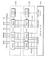
図5は、本発明の実施の形態によるメモリシステムを上から見た図面である。図6は、図5のメモリシステムのブロック図である。図5及び図6に示す構成例において、メモリシステム500は、複数のメモリランク516を制御するメモリコントローラ504を具備する。メモリコントローラ504は、マザーボード502上に装着される。
FIG. 5 is a top view of the memory system according to the embodiment of the present invention. FIG. 6 is a block diagram of the memory system of FIG. 5 and 6, the
メモリコントローラ504の構造及び動作は当業者によく知られているのでその詳しい説明を省略する。
Since the structure and operation of the
複数のメモリランク516は、マザーボード502上に直接装着される。すなわち、図1のメモリシステム100のような分離されたメモリモジュール106を備えていない。それぞれのメモリランクは、バッファ510に連結される複数のメモリ装置508を具備する。
The plurality of
複数のメモリ装置508は、マザーボード502上に直接装着される。それぞれのメモリ装置508は、例えばDRAMまたはSDRAMでありうる。メモリ装置508の構造及び動作は当業者によく知られているので詳しい説明を省略する。
The plurality of
バッファ510は、メモリコントローラ504から受信されるコマンド及びアドレスを制御し、バッファリングする。バッファ510は、コマンド及びアドレスバッファでありうる。バッファ510はマザーボード502上に装着される。バッファ510は、インバータ、ドライバ、及びメモリコントローラ504から受信されるコマンドとアドレス信号とを複数のメモリ装置508にドライブできる装置を備えてもよい。バッファ510の構造及び動作は当業者によく知られているので詳しい説明を省略する。
The
マザーボード502上に信号線が配線される。信号線は、図5及び6に示したようにデータバスDQ、システムクロック信号CLK、及びコマンド及びアドレスバスC/Aを含むことができる。
A signal line is wired on the
メモリシステム500の動作は次の通りである。メモリコントローラ504は、コマンド及びアドレス信号を発生させ、コマンド及びアドレス信号をマザーボード502上に配線されている信号線を介してコマンド及びアドレスバッファ510に伝送する。
The operation of the
メモリ装置508は、データ信号DQ及びシステムクロック信号CLKをコントローラ504から受信したり、またはマザーボード502上の他の回路(図示せず)から受信する。コマンド信号が読出し動作を指示すると、メモリ装置508は、システムクロックCLKに応答してアドレス信号によって指示されたメモリセルから読出されたデータを外部に出力する。
The
コマンド信号が書込み動作を指示すると、メモリ装置508は、システムクロックCLKに応答してアドレス信号によって指示されたメモリセルにデータを書込む。
When the command signal indicates a write operation, the
図5のメモリシステム500では、メモリモジュールを除去することによって信号反射を発生させるスタブ抵抗が除去される。メモリモジュールがなければ、伝送ラインの不連続部を発生させるソケットも必要がない。伝送ラインの不連続部がなければ、前述の問題点として提起されたような、信号反射によって信号線の集積度が減少する問題も除去できる。
In the
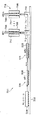
図7は、本発明の実施の形態によるメモリシステムの側面図である。図7に示すシステム700は、図5及び6を参照して説明した複数のメモリランク516及びコントローラ504を備えている。複数のメモリランク516及びコントローラ504はマザーボード502上に装着される。
FIG. 7 is a side view of a memory system according to an embodiment of the present invention. The
図5示すシステム500と異なり、図7に示すシステム700は、メモリモジュール716を具備する。メモリモジュール716は、複数の連結パッド(図示せず)を具備するエッジコネクタ714、複数のメモリ装置708、モジュールボード706、及びC/Aバッファ710を具備し得る。連結パッド(図示せず)は、一般にモジュールボード706の両面に装着される。
Unlike the
複数の受信部、例えばソケット712はマザーボード502に装着される。ソケット712は、エッジコネクタ714と連結されてマザーボード502とメモリモジュール716とを電気的に連結する。
A plurality of receiving units, for example,
特に、ソケット712は、マザーボード502上の信号線をモジュールボード706上の信号線に電気的に連結し、メモリモジュール716をマザーボード502及びコントローラ504に連結させる。
In particular, the
メモリモジュール716は、複数のメモリ装置708を備える。複数のメモリ装置708は、DRAMまたはSDRAMであり得る。バッファ710は、メモリコントローラ504から受信されるコマンドとアドレスを制御してバッファリングする。メモリ装置708及びバッファ710はモジュールボード706上に装着される。
The
メモリモジュール716は、コントローラ504からメモリランク508までの距離よりも遠くに配置される。これにより、マザーボード502上の信号線から分岐される分岐点を除去でき、信号反射を除去できる。
The
分岐点は、分岐点から分岐する方向の数だけ信号を分散させて伝送させる。分岐点においては特性インピーダンス(Z0)の不一致によって意図せぬ信号反射が発生するおそれがある。 At the branch points, signals are distributed and transmitted in the number of directions branching from the branch points. At the branch point, there is a possibility that unintended signal reflection may occur due to mismatch of characteristic impedance (Z0).
コントローラ504とメモリモジュール716との間の信号経路は、コントローラ504からメモリモジュール716のメモリ装置708にまで拡張される。メモリ装置708は、モジュールボード706上に直接ソルダボールにより連結されるので、コントローラ504からメモリ装置708への信号経路には分岐点がなく、その結果、信号反射もない。
The signal path between the
一方、メモリモジュール716がコントローラ504とメモリランク516との間に配置されれば、ソケットはスタブや分岐点を形成する信号線上に配置されなければならない。したがって、このような構造は信号反射を発生させる。
On the other hand, if the
図8は、本発明の実施の形態によるメモリシステム800の側面図である。図8のシステム800は、図7のシステム700が一つのメモリモジュール716だけを持つという点を除けば、図7のシステム700と類似している。
FIG. 8 is a side view of a
図8に示すシステム800は、2つ以上のメモリモジュールを具備することができる。図8に示すシステム800では、マザーボード502から分岐される分岐点が存在するために、図1に示したシステム100の問題点を有しうる。図8に示すシステム800に存在する分岐点は、信号反射を発生させて信号集積度に悪い影響を及ぼす可能性がある。それにもかかわらず、図8のシステム800は、複数のメモリランク516をマザーボード502上に直接装着することによって信号減衰を最小化させ得る。
The
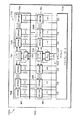
図9は、本発明の実施の形態によるメモリシステム900を上から見た図面である。図9に示すシステム900は、それぞれのメモリランク516内に位相同期ループ520をさらに具備するという点を除けば、図5のシステム500と類似している。
FIG. 9 is a top view of the
位相同期ループ520は、システムクロックCLKに応答して第1クロックを発生させる。位相同期ループ520は、第1クロックを対応するメモリ装置508に印加する。位相同期ループ520により、システム900は、システムクロックCLKをコントローラ504からそれぞれのメモリ装置508に分離させて伝送する必要がなくなる。
The phase locked
他の実施の形態として、位相同期ループ520は、位相同期ループ520と同様に動作する遅延同期ループ(図示せず)に置換えられうる。すなわち、遅延同期ループは、システムクロックCLKに応答して第1クロックを発生し、第1クロックを対応するメモリ装置508に印加する。
As another embodiment, the phase locked
図10は、本発明の実施の形態によるメモリシステム1000を上から見た図面である。図10に示すシステム1000は、メモリモジュール716をさらに具備する点を除けば図9のシステム900と類似している。メモリモジュール716は、図7において説明されたものと同様に動作する。
FIG. 10 is a top view of the
メモリモジュール716は、システムクロックCLKに応答して第1クロックを発生する位相同期ループ720とモジュールボード706とを備える。位相同期ループ720は、第1クロックをメモリモジュール716の対応するメモリ装置708に印加する。
The
位相同期ループ520、720により、システム1000は、システムクロックCLKをコントローラ504からそれぞれのメモリ装置508、708に分離させて伝送する必要がなくなる。
The phase-locked
他の実施の形態として、位相同期ループ520、720は、位相同期ループ520、720と同様に動作する遅延同期ループ(図示せず)に置換えられうる。すなわち、遅延同期ループは、システムクロックCLKに応答して第1クロックを発生し、第1クロックを対応するメモリ装置508、708に印加する。
As another embodiment, the phase locked
少なくとも一つの第1メモリ装置708は、マザーボード上に配線されている第2コマンド及びアドレス信号線を介してコマンド及びアドレスバッファからコマンド及びアドレス信号を受信する。第1コマンド及びアドレス信号線は、第2コマンド及びアドレス信号線と垂直に配置される。
At least one
以上のように、図面及び明細書において最適の実施の形態が開示された。ここで特定用語が使われたが、これは単に本発明を具体的に説明するための目的として使われたものであり、意味限定や特許請求の範囲に記載された本発明の範囲を制限するために使われたものではない。したがって、当業者ならば、これより多様な変形及び均等な他の実施の形態の採用が可能であるといる点を理解しうる。したがって、本発明の真の技術的保護範囲は特許請求の範囲によってのみ決まるべきである。 As described above, the optimum embodiment has been disclosed in the drawings and specification. Although specific terms are used herein, they are merely used for the purpose of specifically explaining the present invention, and limit the scope of the present invention described in the meaning limitation or claims. It was not used for that purpose. Therefore, those skilled in the art can understand that various modifications and equivalent other embodiments can be adopted. Therefore, the true technical protection scope of the present invention should be determined only by the claims.
本発明は、半導体メモリ装置分野に利用でき、特にメモリモジュールを用いた半導体メモリシステム構成に利用できる。 The present invention can be used in the field of semiconductor memory devices, and in particular, can be used in a semiconductor memory system configuration using a memory module.
500 メモリシステム
502 マザーボード
504 メモリコントローラ
508 メモリ装置
510 バッファ
516 メモリランク
500
Claims (37)
前記マザーボードに直接装着され、前記第1バッファに連結される少なくとも一つの第1メモリ装置と、
前記マザーボード上において前記第1バッファ及び前記少なくとも一つの第1メモリ装置に配線される複数の信号線と、を備え、
第1クロック信号線上のシステムクロック信号に応答して第2クロック信号線上の第1クロック信号を発生し、前記マザーボード上に直接装着されるクロック同期回路を備え、
前記少なくとも一つの第1メモリ装置は前記第1クロック信号に同期して動作し、前記クロック同期回路は位相同期ループまたは遅延同期ループのうちいずれか一つであることを特徴とするメモリシステム。 A first buffer mounted directly on the motherboard;
At least one first memory device mounted directly on the motherboard and coupled to the first buffer;
A plurality of signal lines wired to the first buffer and the at least one first memory device on the motherboard;
A clock synchronization circuit for generating a first clock signal on a second clock signal line in response to a system clock signal on the first clock signal line and mounted directly on the motherboard;
The memory system, wherein the at least one first memory device operates in synchronization with the first clock signal, and the clock synchronization circuit is one of a phase locked loop and a delay locked loop.
前記マザーボード上に配線されている第1コマンド及びアドレス信号線を介してコマンド及びアドレス信号を受信することを特徴とする請求項2に記載のメモリシステム。 The command and address buffer
3. The memory system according to claim 2, wherein a command and an address signal are received through a first command and an address signal line wired on the motherboard.
前記マザーボード上に配線されている第2コマンド及びアドレス信号線を介して前記コマンド及びアドレスバッファから前記コマンド及びアドレス信号を受信し、
前記第1コマンド及びアドレス信号線は、前記第2コマンド及びアドレス信号線と垂直に配置されることを特徴とする請求項3に記載のメモリシステム。 The at least one first memory device includes:
Receiving the command and address signal from the command and address buffer via a second command and address signal line wired on the motherboard;
4. The memory system according to claim 3, wherein the first command and address signal lines are disposed perpendicular to the second command and address signal lines.
前記少なくとも一つのメモリモジュールのモジュールボード上に装着される第2バッファと、
前記少なくとも一つのメモリモジュールのモジュールボード上に装着され前記第2バッファに連結される少なくとも一つの第2メモリ装置と、を備えることを特徴とする請求項7に記載のメモリシステム。 The at least one memory module includes:
A second buffer mounted on a module board of the at least one memory module;
The memory system of claim 7, further comprising: at least one second memory device mounted on a module board of the at least one memory module and coupled to the second buffer.
前記マザーボード上における前記メモリコントローラから前記少なくとも一つの第1メモリ装置までの距離よりも遠くに配置されることを特徴とする請求項7に記載のメモリシステム。 The at least one memory module includes:
The memory system according to claim 7, wherein the memory system is disposed farther than a distance from the memory controller to the at least one first memory device on the motherboard.
前記マザーボード上において前記少なくとも一つのメモリランクに配線される複数の信号線と、を備え、
前記少なくとも一つのメモリランクは、
少なくとも一つの第1メモリ装置と、
アドレス及びコマンド信号を前記少なくとも一つの第1メモリ装置に前記マザーボード上の対応する信号線を介してドライビングする第1バッファと、を備え
第1クロック信号線上のシステムクロック信号に応答して第2クロック信号線上の第1クロック信号を発生し、前記マザーボード上に直接装着されるクロック同期回路を備え、
前記少なくとも一つの第1メモリ装置は前記第1クロック信号に同期して動作し、前記クロック同期回路は位相同期ループまたは遅延同期ループのうちいずれか一つであることを特徴とするメモリシステム。 At least one memory rank mounted directly on the motherboard;
A plurality of signal lines wired to the at least one memory rank on the motherboard,
The at least one memory rank is
At least one first memory device;
A first buffer for driving an address and a command signal to the at least one first memory device via a corresponding signal line on the motherboard; and a second clock in response to a system clock signal on the first clock signal line. Generating a first clock signal on the signal line, and comprising a clock synchronization circuit mounted directly on the motherboard;
The memory system, wherein the at least one first memory device operates in synchronization with the first clock signal, and the clock synchronization circuit is one of a phase locked loop and a delay locked loop.
前記マザーボード上に配線されている第1コマンド及びアドレス信号線を介してコマンド及びアドレス信号を受信することを特徴とする請求項13に記載のメモリシステム。 At least one of the first buffers is
14. The memory system according to claim 13, wherein a command and an address signal are received through a first command and an address signal line wired on the motherboard.
前記マザーボード上に配線されている第2コマンド及びアドレス信号線を介して前記少なくとも一つの第1バッファから前記コマンド及びアドレス信号を受信し、
前記第1コマンド及びアドレス信号線は、前記第2コマンド及びアドレス信号線と垂直に配置されていることを特徴とする請求項14に記載のメモリシステム。 The at least one first memory device includes:
Receiving the command and address signal from the at least one first buffer via a second command and address signal line wired on the motherboard;
15. The memory system according to claim 14, wherein the first command and address signal lines are disposed perpendicular to the second command and address signal lines.
前記マザーボード上に装着され、前記メモリモジュールと連結される受信部を備えることを特徴とする請求項15に記載のメモリシステム。 A memory module;
16. The memory system according to claim 15, further comprising a receiving unit mounted on the motherboard and connected to the memory module.
前記メモリモジュールのモジュールボード上に装着されている複数の第2メモリ装置と、
前記メモリモジュールのモジュールボード上に装着され、前記複数の第2メモリ装置をドライビングできる第2バッファと、を備えることを特徴とする請求項20に記載のメモリシステム。 The memory module is
A plurality of second memory devices mounted on a module board of the memory module;
21. The memory system according to claim 20, further comprising: a second buffer mounted on a module board of the memory module and capable of driving the plurality of second memory devices.
マザーボード上においてメモリコントローラから前記少なくとも一つの第1メモリ装置までの距離よりも遠くに配置されることを特徴とする請求項20に記載のメモリシステム。 The receiver is
The memory system of claim 20, characterized in that it is disposed farther than the distance of the motherboard on odor Te from memory controller to the at least one first memory device.
対応するコマンド及びアドレス信号を前記マザーボード上の前記複数の第1メモリ装置にドライビングできる第1コマンド及びアドレスバッファを直接装着する段階と、を備え、
第1クロック信号線上のシステムクロック信号に応答して第2クロック信号線上の第1クロック信号を発生し、前記マザーボード上に直接装着されるクロック同期回路を備え、
前記少なくとも一つの第1メモリ装置は前記第1クロック信号に同期して動作し、前記クロック同期回路は位相同期ループまたは遅延同期ループのうちいずれか一つであることを特徴とするメモリシステムの構成方法。 Directly mounting a plurality of first memory devices on a motherboard;
Directly mounting a first command and address buffer capable of driving corresponding command and address signals to the plurality of first memory devices on the motherboard,
A clock synchronization circuit for generating a first clock signal on a second clock signal line in response to a system clock signal on the first clock signal line and mounted directly on the motherboard;
The memory system is characterized in that the at least one first memory device operates in synchronization with the first clock signal, and the clock synchronization circuit is one of a phase locked loop and a delay locked loop. Method.
前記モジュールボード上に第2コマンド及びアドレスバッファを装着する段階と、を具備えており、
前記モジュールボードは、前記マザーボード上に装着されているソケットを通じてメモリコントローラに連結されることを特徴とする請求項26に記載のメモリシステムの構成方法。 Mounting a second memory device on a module board of the memory module;
Mounting a second command and an address buffer on the module board,
27. The method according to claim 26, wherein the module board is connected to a memory controller through a socket mounted on the motherboard.
前記マザーボード上に直接装着され、前記コマンド及びアドレス信号を受信する第1バッファと、
前記マザーボード上に直接装着され、前記第1バッファに連結される少なくとも一つの第1メモリ装置と、
前記マザーボード上において前記第1バッファ及び前記少なくとも一つの第1メモリ装置に配線される複数の信号線と、を備え、
第1クロック信号線上のシステムクロック信号に応答して第2クロック信号線上の第1クロック信号を発生し、前記マザーボード上に直接装着されるクロック同期回路を備え、
前記少なくとも一つの第1メモリ装置は前記第1クロック信号に同期して動作し、前記クロック同期回路は位相同期ループまたは遅延同期ループのうちいずれか一つであることを特徴とするメモリシステム。 A memory controller that is directly attached to the motherboard and generates a plurality of command and address signals;
A first buffer mounted directly on the motherboard and receiving the command and address signals;
At least one first memory device mounted directly on the motherboard and coupled to the first buffer;
A plurality of signal lines wired to the first buffer and the at least one first memory device on the motherboard;
A clock synchronization circuit for generating a first clock signal on a second clock signal line in response to a system clock signal on the first clock signal line and mounted directly on the motherboard;
The memory system, wherein the at least one first memory device operates in synchronization with the first clock signal, and the clock synchronization circuit is one of a phase locked loop and a delay locked loop.
前記マザーボード上に直接装着され、前記コマンド及びアドレス信号を受信する第1バッファと、
前記マザーボード上に直接装着され、前記第1バッファに連結する少なくとも一つの第1メモリ装置と、
少なくとも一つのメモリモジュールは、モジュールボード上に装着され前記コマンド及びアドレス信号を受信する第2バッファと、前記第2バッファに連結され前記少なくとも一つの第1メモリ装置よりも前記メモリコントローラから遠い位置において前記モジュールボード上に装着される少なくとも一つの第2メモリ装置と、を具備する少なくとも一つのメモリモジュールと、
前記マザーボード上において前記第1バッファ及び前記少なくとも一つの第1メモリ装置に配線される複数の第1信号線と、
前記モジュールボード上における前記第2バッファ及び前記少なくとも一つの第2メモリ装置に配線される複数の第2信号線と、を備え、
第1クロック信号線上のシステムクロック信号に応答して第2クロック信号線上の第1クロック信号を発生し、前記マザーボード上に直接装着されるクロック同期回路を備え、
前記少なくとも一つの第1メモリ装置は前記第1クロック信号に同期して動作し、前記クロック同期回路は位相同期ループまたは遅延同期ループのうちいずれか一つであることを特徴とするメモリシステム。 A memory controller that is directly attached to the motherboard and generates a plurality of command and address signals;
A first buffer mounted directly on the motherboard and receiving the command and address signals;
At least one first memory device mounted directly on the motherboard and coupled to the first buffer ;
One memory module even without least includes a second buffer mounted on the module board to receive the command and address signals from the memory controller than the coupled to the second buffer at least one first memory device At least one second memory device mounted on the module board at a remote location, and at least one memory module comprising:
A plurality of first signal lines wired to the first buffer and the at least one first memory device on the motherboard;
A plurality of second signal lines wired to the second buffer and the at least one second memory device on the module board;
A clock synchronization circuit for generating a first clock signal on a second clock signal line in response to a system clock signal on the first clock signal line and mounted directly on the motherboard;
The memory system, wherein the at least one first memory device operates in synchronization with the first clock signal, and the clock synchronization circuit is one of a phase locked loop and a delay locked loop.
前記マザーボード上に直接装着され、前記コマンド及びアドレス信号を受信する第1バッファと、
前記マザーボード上に直接装着され、クロック信号を受信する位相同期ループと、
前記マザーボード上に直接装着され、前記第1バッファに連結される少なくとも一つの第1メモリ装置と、
前記マザーボード上において前記第1バッファ及び前記少なくとも一つの第1メモリ装置に配線される複数の信号線を備えており、
前記第1メモリ装置は、前記位相同期ループから出力される内部クロック信号に同期して動作することを特徴とするメモリシステム。 A memory controller that is directly attached to the motherboard and generates a plurality of command and address signals;
A first buffer mounted directly on the motherboard and receiving the command and address signals;
A phase-locked loop mounted directly on the motherboard and receiving a clock signal;
At least one first memory device mounted directly on the motherboard and coupled to the first buffer;
A plurality of signal lines wired to the first buffer and the at least one first memory device on the motherboard;
The memory system, wherein the first memory device operates in synchronization with an internal clock signal output from the phase locked loop.
前記マザーボード上に直接装着され、前記コマンド及びアドレス信号を受信する第1バッファと、
前記マザーボード上に直接装着され、クロック信号を受信する第1位相同期ループと、
前記マザーボード上に直接装着され、前記第1バッファに連結される少なくとも一つの第1メモリ装置と、
モジュールボード上に装着され、前記コマンド及びアドレス信号を受信する第2バッファと、前記第2バッファに連結され前記少なくとも一つの第1メモリ装置よりも前記メモリコントローラから遠い位置において前記モジュールボード上に装着される少なくとも一つの第2メモリ装置と、を具備する少なくとも一つのメモリモジュールと、
前記マザーボード上に直接装着され、前記クロック信号を受信する第2位相同期ループと、
前記マザーボード上において前記第1バッファ及び前記少なくとも一つの第1メモリ装置に配線される複数の第1信号線と、
前記モジュールボード上において前記第2バッファ及び前記少なくとも一つの第2メモリ装置に配線される複数の第2信号線と、を備えており、
前記第1メモリ装置は、前記第1位相同期ループから出力される第1内部クロック信号に同期して動作し、前記第2メモリ装置は、前記第2位相同期ループから出力される第2内部クロック信号に同期して動作することを特徴とするメモリシステム。 A memory controller that is directly attached to the motherboard and generates a plurality of command and address signals;
A first buffer mounted directly on the motherboard and receiving the command and address signals;
A first phase-locked loop mounted directly on the motherboard and receiving a clock signal;
At least one first memory device mounted directly on the motherboard and coupled to the first buffer;
A second buffer mounted on the module board for receiving the command and address signals; and a second buffer coupled to the second buffer and mounted on the module board at a position farther from the memory controller than the at least one first memory device. At least one second memory device, and at least one memory module comprising:
A second phase-locked loop mounted directly on the motherboard and receiving the clock signal;
A plurality of first signal lines wired to the first buffer and the at least one first memory device on the motherboard;
A plurality of second signal lines wired to the second buffer and the at least one second memory device on the module board;
The first memory device operates in synchronization with a first internal clock signal output from the first phase-locked loop, and the second memory device outputs a second internal clock output from the second phase-locked loop. A memory system which operates in synchronization with a signal.
Applications Claiming Priority (4)
| Application Number | Priority Date | Filing Date | Title |
|---|---|---|---|
| KR10-2003-0028175A KR100532432B1 (en) | 2003-05-02 | 2003-05-02 | Memory system capable of transporting command and address signals fast |
| KR2003-028175 | 2003-05-02 | ||
| US10/750,093 US7227796B2 (en) | 2003-05-02 | 2003-12-31 | Memory system mounted directly on board and associated method |
| US10/750093 | 2003-12-31 |
Publications (3)
| Publication Number | Publication Date |
|---|---|
| JP2004334879A JP2004334879A (en) | 2004-11-25 |
| JP2004334879A5 JP2004334879A5 (en) | 2007-06-14 |
| JP4837899B2 true JP4837899B2 (en) | 2011-12-14 |
Family
ID=33455675
Family Applications (1)
| Application Number | Title | Priority Date | Filing Date |
|---|---|---|---|
| JP2004137797A Expired - Fee Related JP4837899B2 (en) | 2003-05-02 | 2004-05-06 | Memory system and method |
Country Status (5)
| Country | Link |
|---|---|
| US (1) | US7692983B2 (en) |
| JP (1) | JP4837899B2 (en) |
| CN (1) | CN1542839B (en) |
| DE (1) | DE102004022347B4 (en) |
| TW (1) | TWI261269B (en) |
Families Citing this family (10)
| Publication number | Priority date | Publication date | Assignee | Title |
|---|---|---|---|---|
| KR100532432B1 (en) * | 2003-05-02 | 2005-11-30 | 삼성전자주식회사 | Memory system capable of transporting command and address signals fast |
| DE102004022347B4 (en) | 2003-05-02 | 2008-04-03 | Samsung Electronics Co., Ltd., Suwon | Memory system with motherboard and associated mounting procedure |
| US8143720B2 (en) * | 2007-02-06 | 2012-03-27 | Rambus Inc. | Semiconductor module with micro-buffers |
| TW200921595A (en) * | 2007-11-14 | 2009-05-16 | Darfon Electronics Corp | Multi-lamp backlight apparatus |
| US7915912B2 (en) | 2008-09-24 | 2011-03-29 | Rambus Inc. | Signal lines with internal and external termination |
| KR20140037443A (en) * | 2012-09-18 | 2014-03-27 | 삼성전자주식회사 | Memory device and tuning method for thererof |
| US8860479B2 (en) * | 2013-03-15 | 2014-10-14 | Intel Corporation | Integrated clock differential buffering |
| JP6424847B2 (en) * | 2016-02-16 | 2018-11-21 | 京セラドキュメントソリューションズ株式会社 | Transmission apparatus and image forming apparatus provided with the same |
| US11742277B2 (en) | 2018-08-14 | 2023-08-29 | Rambus Inc. | Packaged integrated device having memory buffer integrated circuit asymmetrically positioned on substrate |
| US11757436B2 (en) * | 2021-08-30 | 2023-09-12 | Taiwan Semiconductor Manufacturing Company Ltd. | System for signal propagation and method of operating the same |
Family Cites Families (20)
| Publication number | Priority date | Publication date | Assignee | Title |
|---|---|---|---|---|
| JP2891709B2 (en) * | 1989-01-16 | 1999-05-17 | 株式会社日立製作所 | Semiconductor integrated circuit device |
| JPH08305629A (en) * | 1995-04-25 | 1996-11-22 | Internatl Business Mach Corp <Ibm> | Apparatus and method for control of memory access as well ascomputer system |
| US5650757A (en) * | 1996-03-27 | 1997-07-22 | Hewlett-Packard Company | Impedance stepping for increasing the operating speed of computer backplane busses |
| JP3455040B2 (en) * | 1996-12-16 | 2003-10-06 | 株式会社日立製作所 | Source clock synchronous memory system and memory unit |
| KR100286369B1 (en) * | 1997-01-06 | 2001-04-16 | 윤종용 | Computer system |
| JPH10283256A (en) * | 1997-04-07 | 1998-10-23 | Nec Corp | Memory bus connection system |
| US5896346A (en) * | 1997-08-21 | 1999-04-20 | International Business Machines Corporation | High speed and low cost SDRAM memory subsystem |
| US6108228A (en) * | 1997-12-02 | 2000-08-22 | Micron Technology, Inc. | Quad in-line memory module |
| US6229727B1 (en) * | 1998-09-28 | 2001-05-08 | Cisco Technology, Inc. | Method and apparatus for support of multiple memory devices in a single memory socket architecture |
| US6324071B2 (en) * | 1999-01-14 | 2001-11-27 | Micron Technology, Inc. | Stacked printed circuit board memory module |
| US6414868B1 (en) * | 1999-06-07 | 2002-07-02 | Sun Microsystems, Inc. | Memory expansion module including multiple memory banks and a bank control circuit |
| JP2001022684A (en) * | 1999-07-13 | 2001-01-26 | Toshiba Corp | System substrate and computer system |
| WO2001042893A1 (en) * | 1999-12-10 | 2001-06-14 | Hitachi, Ltd | Semiconductor module |
| JP4569912B2 (en) * | 2000-03-10 | 2010-10-27 | エルピーダメモリ株式会社 | Memory system |
| KR100399594B1 (en) * | 2000-05-04 | 2003-09-26 | 삼성전자주식회사 | system board and impedance control method thereof |
| US7313715B2 (en) * | 2001-02-09 | 2007-12-25 | Samsung Electronics Co., Ltd. | Memory system having stub bus configuration |
| JP3799251B2 (en) * | 2001-08-24 | 2006-07-19 | エルピーダメモリ株式会社 | Memory device and memory system |
| DE10152916B4 (en) * | 2001-10-26 | 2006-11-30 | Infineon Technologies Ag | Information containment device for memory modules and memory chips |
| KR100532432B1 (en) * | 2003-05-02 | 2005-11-30 | 삼성전자주식회사 | Memory system capable of transporting command and address signals fast |
| DE102004022347B4 (en) | 2003-05-02 | 2008-04-03 | Samsung Electronics Co., Ltd., Suwon | Memory system with motherboard and associated mounting procedure |
-
2004
- 2004-04-29 DE DE102004022347A patent/DE102004022347B4/en not_active Expired - Fee Related
- 2004-04-30 TW TW093112332A patent/TWI261269B/en not_active IP Right Cessation
- 2004-05-02 CN CN2004100477286A patent/CN1542839B/en not_active Expired - Fee Related
- 2004-05-06 JP JP2004137797A patent/JP4837899B2/en not_active Expired - Fee Related
-
2007
- 2007-05-08 US US11/745,965 patent/US7692983B2/en active Active
Also Published As
| Publication number | Publication date |
|---|---|
| US20070250658A1 (en) | 2007-10-25 |
| US7692983B2 (en) | 2010-04-06 |
| CN1542839B (en) | 2010-08-25 |
| TWI261269B (en) | 2006-09-01 |
| CN1542839A (en) | 2004-11-03 |
| DE102004022347A1 (en) | 2004-12-09 |
| DE102004022347B4 (en) | 2008-04-03 |
| JP2004334879A (en) | 2004-11-25 |
| TW200519964A (en) | 2005-06-16 |
Similar Documents
| Publication | Publication Date | Title |
|---|---|---|
| US20210271593A1 (en) | Memory module with distributed data buffers | |
| JP4685486B2 (en) | Memory module system that effectively controls ODT | |
| US7692983B2 (en) | Memory system mounted directly on board and associated method | |
| KR100213965B1 (en) | High speed electrical signal interconnect structure | |
| JP4885623B2 (en) | Multilayer semiconductor device | |
| US7274583B2 (en) | Memory system having multi-terminated multi-drop bus | |
| US6937494B2 (en) | Memory module, memory chip, and memory system | |
| JP3821678B2 (en) | Memory device | |
| US6530033B1 (en) | Radial arm memory bus for a high availability computer system | |
| EP3208806B1 (en) | Termination topology of memory system and associated memory module and control method | |
| US7542305B2 (en) | Memory module having on-package or on-module termination | |
| WO1999046687A1 (en) | Data transmitter | |
| US8233304B2 (en) | High speed memory module | |
| US8053911B2 (en) | Semiconductor device and data processor | |
| US7227796B2 (en) | Memory system mounted directly on board and associated method | |
| JP2007164599A (en) | Memory module | |
| JP2005085267A (en) | Circuit for memory module address bus and system for addressing memory module | |
| JP2005310153A (en) | Memory device | |
| JP4695361B2 (en) | Stacked memory module and memory system | |
| JP2008071474A (en) | Boosted clock circuit for semiconductor memory | |
| US6272195B1 (en) | Method and apparatus for correcting signal skew differentials between two interconnected devices | |
| KR20230149691A (en) | Semiconductor die for controlling on-die-termination of another semiconductor die, and semiconductor devices having the same | |
| GB2388714A (en) | A method and apparatus for interconnecting multiple devices on a circuit board |
Legal Events
| Date | Code | Title | Description |
|---|---|---|---|
| A521 | Request for written amendment filed |
Free format text: JAPANESE INTERMEDIATE CODE: A523 Effective date: 20070424 |
|
| A621 | Written request for application examination |
Free format text: JAPANESE INTERMEDIATE CODE: A621 Effective date: 20070424 |
|
| RD03 | Notification of appointment of power of attorney |
Free format text: JAPANESE INTERMEDIATE CODE: A7423 Effective date: 20080201 |
|
| RD04 | Notification of resignation of power of attorney |
Free format text: JAPANESE INTERMEDIATE CODE: A7424 Effective date: 20080616 |
|
| A977 | Report on retrieval |
Free format text: JAPANESE INTERMEDIATE CODE: A971007 Effective date: 20100804 |
|
| A131 | Notification of reasons for refusal |
Free format text: JAPANESE INTERMEDIATE CODE: A131 Effective date: 20100810 |
|
| A521 | Request for written amendment filed |
Free format text: JAPANESE INTERMEDIATE CODE: A523 Effective date: 20101110 |
|
| A131 | Notification of reasons for refusal |
Free format text: JAPANESE INTERMEDIATE CODE: A131 Effective date: 20110510 |
|
| A521 | Request for written amendment filed |
Free format text: JAPANESE INTERMEDIATE CODE: A523 Effective date: 20110805 |
|
| TRDD | Decision of grant or rejection written | ||
| A01 | Written decision to grant a patent or to grant a registration (utility model) |
Free format text: JAPANESE INTERMEDIATE CODE: A01 Effective date: 20110830 |
|
| A01 | Written decision to grant a patent or to grant a registration (utility model) |
Free format text: JAPANESE INTERMEDIATE CODE: A01 |
|
| A61 | First payment of annual fees (during grant procedure) |
Free format text: JAPANESE INTERMEDIATE CODE: A61 Effective date: 20110929 |
|
| FPAY | Renewal fee payment (event date is renewal date of database) |
Free format text: PAYMENT UNTIL: 20141007 Year of fee payment: 3 |
|
| R150 | Certificate of patent or registration of utility model |
Free format text: JAPANESE INTERMEDIATE CODE: R150 |
|
| LAPS | Cancellation because of no payment of annual fees |