JP4836780B2 - Method of cleaning a processing chamber in a substrate processing apparatus and a method for detecting an end point of cleaning - Google Patents
Method of cleaning a processing chamber in a substrate processing apparatus and a method for detecting an end point of cleaning Download PDFInfo
- Publication number
- JP4836780B2 JP4836780B2 JP2006510214A JP2006510214A JP4836780B2 JP 4836780 B2 JP4836780 B2 JP 4836780B2 JP 2006510214 A JP2006510214 A JP 2006510214A JP 2006510214 A JP2006510214 A JP 2006510214A JP 4836780 B2 JP4836780 B2 JP 4836780B2
- Authority
- JP
- Japan
- Prior art keywords
- gas
- cleaning
- plasma
- processing
- substrate
- Prior art date
- Legal status (The legal status is an assumption and is not a legal conclusion. Google has not performed a legal analysis and makes no representation as to the accuracy of the status listed.)
- Active
Links
Images


Classifications
-
- H—ELECTRICITY
- H01—ELECTRIC ELEMENTS
- H01J—ELECTRIC DISCHARGE TUBES OR DISCHARGE LAMPS
- H01J37/00—Discharge tubes with provision for introducing objects or material to be exposed to the discharge, e.g. for the purpose of examination or processing thereof
- H01J37/32—Gas-filled discharge tubes
- H01J37/32917—Plasma diagnostics
- H01J37/32935—Monitoring and controlling tubes by information coming from the object and/or discharge
-
- H—ELECTRICITY
- H01—ELECTRIC ELEMENTS
- H01L—SEMICONDUCTOR DEVICES NOT COVERED BY CLASS H10
- H01L21/00—Processes or apparatus adapted for the manufacture or treatment of semiconductor or solid state devices or of parts thereof
- H01L21/02—Manufacture or treatment of semiconductor devices or of parts thereof
- H01L21/04—Manufacture or treatment of semiconductor devices or of parts thereof the devices having at least one potential-jump barrier or surface barrier, e.g. PN junction, depletion layer or carrier concentration layer
- H01L21/18—Manufacture or treatment of semiconductor devices or of parts thereof the devices having at least one potential-jump barrier or surface barrier, e.g. PN junction, depletion layer or carrier concentration layer the devices having semiconductor bodies comprising elements of Group IV of the Periodic System or AIIIBV compounds with or without impurities, e.g. doping materials
- H01L21/30—Treatment of semiconductor bodies using processes or apparatus not provided for in groups H01L21/20 - H01L21/26
- H01L21/302—Treatment of semiconductor bodies using processes or apparatus not provided for in groups H01L21/20 - H01L21/26 to change their surface-physical characteristics or shape, e.g. etching, polishing, cutting
- H01L21/304—Mechanical treatment, e.g. grinding, polishing, cutting
-
- B—PERFORMING OPERATIONS; TRANSPORTING
- B08—CLEANING
- B08B—CLEANING IN GENERAL; PREVENTION OF FOULING IN GENERAL
- B08B7/00—Cleaning by methods not provided for in a single other subclass or a single group in this subclass
- B08B7/0035—Cleaning by methods not provided for in a single other subclass or a single group in this subclass by radiant energy, e.g. UV, laser, light beam or the like
-
- H—ELECTRICITY
- H01—ELECTRIC ELEMENTS
- H01J—ELECTRIC DISCHARGE TUBES OR DISCHARGE LAMPS
- H01J37/00—Discharge tubes with provision for introducing objects or material to be exposed to the discharge, e.g. for the purpose of examination or processing thereof
- H01J37/32—Gas-filled discharge tubes
- H01J37/32009—Arrangements for generation of plasma specially adapted for examination or treatment of objects, e.g. plasma sources
- H01J37/32192—Microwave generated discharge
-
- H—ELECTRICITY
- H01—ELECTRIC ELEMENTS
- H01J—ELECTRIC DISCHARGE TUBES OR DISCHARGE LAMPS
- H01J37/00—Discharge tubes with provision for introducing objects or material to be exposed to the discharge, e.g. for the purpose of examination or processing thereof
- H01J37/32—Gas-filled discharge tubes
- H01J37/32431—Constructional details of the reactor
- H01J37/32798—Further details of plasma apparatus not provided for in groups H01J37/3244 - H01J37/32788; special provisions for cleaning or maintenance of the apparatus
- H01J37/32853—Hygiene
- H01J37/32862—In situ cleaning of vessels and/or internal parts
-
- H—ELECTRICITY
- H01—ELECTRIC ELEMENTS
- H01L—SEMICONDUCTOR DEVICES NOT COVERED BY CLASS H10
- H01L21/00—Processes or apparatus adapted for the manufacture or treatment of semiconductor or solid state devices or of parts thereof
- H01L21/02—Manufacture or treatment of semiconductor devices or of parts thereof
- H01L21/04—Manufacture or treatment of semiconductor devices or of parts thereof the devices having at least one potential-jump barrier or surface barrier, e.g. PN junction, depletion layer or carrier concentration layer
- H01L21/18—Manufacture or treatment of semiconductor devices or of parts thereof the devices having at least one potential-jump barrier or surface barrier, e.g. PN junction, depletion layer or carrier concentration layer the devices having semiconductor bodies comprising elements of Group IV of the Periodic System or AIIIBV compounds with or without impurities, e.g. doping materials
- H01L21/30—Treatment of semiconductor bodies using processes or apparatus not provided for in groups H01L21/20 - H01L21/26
- H01L21/302—Treatment of semiconductor bodies using processes or apparatus not provided for in groups H01L21/20 - H01L21/26 to change their surface-physical characteristics or shape, e.g. etching, polishing, cutting
- H01L21/306—Chemical or electrical treatment, e.g. electrolytic etching
- H01L21/3065—Plasma etching; Reactive-ion etching
Description
本発明は、基板処理装置における処理室のクリーニング方法およびクリーニングの終点検出方法に関し、より詳しくは、金属で汚染された処理室のクリーニング方法、およびクリーニングの終点検出方法、ならびにその方法を実行するためのコンピュータプログラムおよび記録媒体に関する。 The present invention relates to a processing chamber cleaning method and cleaning end point detection method in a substrate processing apparatus, and more particularly, to a processing chamber cleaning method contaminated with metal, a cleaning end point detection method, and a method for executing the method. The present invention relates to a computer program and a recording medium.
近時、LSIの高集積化、高速化の要請からLSIを構成する半導体素子のデザインルールが益々微細化されており、それにともなって、DRAM等に用いられるトランジスタのゲート電極の低抵抗化が求められている。そのため、より抵抗の低いW系膜がゲート電極として用いられつつあり、タングステンポリサイド(WSi/poly−Siの積層膜)や、より抵抗の低いタングステンポリメタルゲート(W/WN/poly−Siの積層構造)が注目されている。 In recent years, design rules for semiconductor elements constituting LSIs have become increasingly finer due to demands for higher integration and higher speeds of LSIs, and accordingly, resistance of gate electrodes of transistors used in DRAMs and the like has been reduced. It has been. Therefore, a W-based film having a lower resistance is being used as a gate electrode, and tungsten polycide (a laminated film of WSi / poly-Si) or a tungsten polymetal gate having a lower resistance (W / WN / poly-Si). (Laminated structure) is attracting attention.
一方、このようなタングステンポリメタルゲートやタングステンポリサイドを用いたゲート電極の製造プロセスにおいて、その側面のポリシリコンを選択酸化する工程が存在するが、その際に、タングステン酸化物を抑制しつつポリシリコンを選択酸化する観点から、プラズマ密度が高い低電子温度プラズマにより低温処理が可能な、RLSA(Radial Line Slot Antenna)マイクロ波プラズマ処理装置が用いられている(例えば特許文献1)。 On the other hand, in the process of manufacturing a gate electrode using such a tungsten polymetal gate or tungsten polycide, there is a step of selectively oxidizing the polysilicon on the side surface. From the viewpoint of selective oxidation of silicon, an RLSA (Radial Line Slot Antenna) microwave plasma processing apparatus capable of performing low temperature processing with low electron temperature plasma having a high plasma density is used (for example, Patent Document 1).
このような処理においては、タングステンを含むSiウエハを処理することとなり、処理後の処理チャンバーはタングステンで汚染された状態となる。このような処理チャンバーで次の選択酸化処理を行う場合には、タングステンが処理に悪影響を与え、タングステンがコンタミネーションとして素子に取り込まれるおそれがある他、タングステンによって酸化処理が妨げられ酸化レートが低下してしまう。したがって、処理後の処理チャンバーは、クリーニングにより汚染レベルを半導体素子を製造可能なレベルまで低下させる必要がある。 In such a process, a Si wafer containing tungsten is processed, and the process chamber after the process is contaminated with tungsten. When performing the next selective oxidation process in such a processing chamber, tungsten may adversely affect the process, and tungsten may be taken into the element as a contamination. In addition, the oxidation process is hindered by tungsten and the oxidation rate is lowered. Resulting in. Therefore, it is necessary to reduce the contamination level of the processing chamber after processing to a level at which a semiconductor element can be manufactured by cleaning.
従来、このようなタングステン(W)で汚染された処理チャンバーのクリーニングは、処理チャンバーを大気開放して、チャンバー内部部品を酸などでウェットクリーニングし、それに加えて真空チャンバー内壁を酸、水、または溶剤をしみこませたワイパーにより拭き取ることによって行っている。 Conventionally, the processing chamber contaminated with tungsten (W) is cleaned by opening the processing chamber to the atmosphere, wet-cleaning the chamber internal parts with acid or the like, and in addition, the inner wall of the vacuum chamber with acid, water, or This is done by wiping with a wiper soaked with solvent.
しかしながら、このようにクリーニングする場合には、処理チャンバーを大気開放する時間、ウェット洗浄する時間、再排気する時間、および排気後の処理チャンバーを再コンデショニングする時間等、数時間単位の時間を要し、スループットが低くなる原因となっている。 However, such cleaning requires several hours such as the time for opening the processing chamber to the atmosphere, the time for wet cleaning, the time for re-evacuation, and the time for re-conditioning the processing chamber after evacuation. However, this is a cause of low throughput.
一方、プラズマを用いたドライクリーニング方法も検討されている。プラズマによるドライクリーニングは、一般に、クリーニングガスをプラズマ化してチャンバー内に付着した堆積物を除去する方法である。 On the other hand, a dry cleaning method using plasma is also being studied. In general, dry cleaning using plasma is a method in which a cleaning gas is turned into plasma to remove deposits deposited in the chamber.
しかしながら、従来はドライクリーニングを用いても、タングステン(W)等の金属で汚染された処理室を高効率で清浄化することは未だ成功していない。 However, conventionally, even if dry cleaning is used, it has not been successful yet to clean a processing chamber contaminated with a metal such as tungsten (W) with high efficiency.
また、ドライクリーニングにおいては、終点の判断が困難であるため、クリーニングの終了を時間管理で判断している。しかし、時間管理による場合は、予め設定した時間を基準にクリーニングを終了させるため、クリーニングが不十分であったり、逆にクリーニング時間が長すぎる等の不都合が生じる。クリーニングが不十分な場合は、チャンバー内に残留した堆積物がコンタミネーションを引き起こすため、再度クリーニングをやり直さなければならず煩雑であり、逆にクリーニング時間が長すぎる場合は、その分の時間とエネルギーが無駄に浪費されてしまう。
本発明の目的は、基板処理装置におけるタングステン等の金属で汚染された処理室を、高効率で清浄化することができる、基板処理装置における処理室のクリーニング方法を提供することにある。 An object of the present invention is to provide a method for cleaning a processing chamber in a substrate processing apparatus, which can clean a processing chamber contaminated with a metal such as tungsten in the substrate processing apparatus with high efficiency.
本発明の他の目的は、基板処理装置におけるタングステン等の金属で汚染された処理室を清浄化する際に、簡易な方法で終点を把握できるクリーニングの終点検出方法およびクリーニング方法を提供することにある。 Another object of the present invention is to provide a cleaning end point detection method and cleaning method capable of grasping an end point by a simple method when cleaning a processing chamber contaminated with a metal such as tungsten in a substrate processing apparatus. is there.
本発明の第1の観点によれば、基板に対して減圧処理を施す基板処理装置における金属で汚染された処理室をクリーニングするクリーニング方法であって、前記処理後、大気開放することなく前記処理室内にO 2 ガス単独、またはO 2 ガスおよび不活性ガスを導入し、このガスのプラズマを形成して前記処理室をクリーニングする、基板処理装置における処理室のクリーニング方法が提供される。
本発明の第2の観点によれば、基板に対して減圧処理を施す基板処理装置における金属で汚染された処理室をクリーニングするクリーニング方法であって、前記処理後、大気開放することなく前記処理室内にO 2 ガスおよびH 2 ガスおよび不活性ガス、またはO 2 ガスおよびH 2 ガスを導入し、これらのガスのプラズマを形成して前記処理室をクリーニングする、基板処理装置における処理室のクリーニング方法が提供される。
According to a first aspect of the present invention, there is provided a cleaning method for cleaning a processing chamber contaminated with metal in a substrate processing apparatus that performs a decompression process on a substrate, and the processing is performed without opening to the atmosphere after the processing. There is provided a method for cleaning a processing chamber in a substrate processing apparatus, wherein O 2 gas alone or an O 2 gas and an inert gas are introduced into the chamber, and plasma of the gas is formed to clean the processing chamber.
According to a second aspect of the present invention, there is provided a cleaning method for cleaning a processing chamber contaminated with a metal in a substrate processing apparatus for performing a decompression process on a substrate, wherein the processing is performed without opening to the atmosphere after the processing. Cleaning of a processing chamber in a substrate processing apparatus, wherein O 2 gas and H 2 gas and inert gas, or O 2 gas and H 2 gas are introduced into the chamber, and plasma of these gases is formed to clean the processing chamber. A method is provided.
本発明の第3の観点によれば、金属を含む膜を有する基板にプラズマ処理を施す基板処理装置における処理室をクリーニングするクリーニング方法であって、前記処理後、大気開放することなく前記処理室内にO 2 ガス単独、またはO 2 ガスおよび不活性ガスを導入し、このガスのプラズマを形成して前記処理室をクリーニングする、基板処理装置における処理室のクリーニング方法が提供される。
本発明の第4の観点によれば、金属を含む膜を有する基板にプラズマ処理を施す基板処理装置における処理室をクリーニングするクリーニング方法であって、前記処理後、大気開放することなく前記処理室内にO 2 ガスおよびH 2 ガスおよび不活性ガス、またはO 2 ガスおよびH 2 ガスを導入し、これらのガスのプラズマを形成して前記処理室をクリーニングする、基板処理装置における処理室のクリーニング方法が提供される。
According to a third aspect of the present invention, there is provided a cleaning method for cleaning a processing chamber in a substrate processing apparatus for performing plasma processing on a substrate having a metal-containing film, wherein the processing chamber is not opened to the atmosphere after the processing. There is provided a method for cleaning a processing chamber in a substrate processing apparatus, wherein O 2 gas alone, or O 2 gas and an inert gas are introduced, and plasma of the gas is formed to clean the processing chamber.
According to a fourth aspect of the present invention, there is provided a cleaning method for cleaning a processing chamber in a substrate processing apparatus for performing plasma processing on a substrate having a metal-containing film, wherein the processing chamber is not opened to the atmosphere after the processing. A cleaning method for a processing chamber in a substrate processing apparatus, wherein O 2 gas and H 2 gas and inert gas, or O 2 gas and H 2 gas are introduced into the substrate, and plasma of these gases is formed to clean the processing chamber Is provided.
上記第1および第2の観点において、前記基板の処理としては、金属を含む基板の酸化処理を提供することができる。また、前記金属の典型例としてタングステンを挙げることができる。さらに、前記基板の処理としては、プラズマ処理を適用することができる。 In the first and second aspects, as the treatment of the substrate, an oxidation treatment of a substrate containing a metal can be provided. A typical example of the metal is tungsten. Further, plasma processing can be applied as the processing of the substrate.
上記第3および第4の観点において、前記金属を含む膜として、タングステン系膜を用いることができ、具体的なプラズマ処理としては、タングステン系膜とポリシリコン膜とを含むゲート電極の選択酸化処理を適用することができる。 In the third and fourth aspects, a tungsten-based film can be used as the film containing the metal. As a specific plasma process, a selective oxidation process of a gate electrode including a tungsten-based film and a polysilicon film is used. Can be applied.
上記第1および第2の観点においてプラズマ処理を適用する場合、ならびに上記第3および第4の観点において、前記基板のプラズマ処理およびクリーニングは、平面アンテナを用いたプラズマまたは誘導結合型プラズマを用いたプラズマにより実施することができる。また、前記基板のプラズマ処理および前記クリーニングは、複数のスロットを有する平面アンテナにて前記処理室内にマイクロ波を導入して形成されるプラズマにより実施されることが好ましい。 In the case where the plasma treatment is applied in the first and second aspects, and in the third and fourth aspects, the plasma treatment and cleaning of the substrate are performed using plasma using a planar antenna or inductively coupled plasma. It can be implemented by plasma. Moreover, it is preferable that the plasma treatment and the cleaning of the substrate be performed by plasma formed by introducing a microwave into the treatment chamber using a planar antenna having a plurality of slots.
上記第2および第4の観点において、前記クリーニングを実施するプラズマのO2ガスに対するH2ガスの比が4以上であることが好ましく、8であることが特に好ましい。また、上記第1〜第4の観点において、前記クリーニングは、処理室内の温度を400〜800℃にして行うことが好ましい。さらに、前記クリーニングは、処理室内の圧力を126Pa未満にして行うことが好ましい。 In the second and fourth aspects, the ratio of the H 2 gas to the O 2 gas of the plasma for performing the cleaning is preferably 4 or more, and particularly preferably 8. In the first to fourth aspects, the cleaning is preferably performed at a temperature in the processing chamber of 400 to 800 ° C. Furthermore, it is preferable that the cleaning is performed with the pressure in the processing chamber being less than 126 Pa .
また、前記クリーニングに先立って、前記処理室をプラズマにより加熱してもよい。前記基板処理装置としては、前記処理室のプラズマに曝される面の少なくとも一部が誘電体で構成されているものを好適に用いることができる。 Further, prior to the previous SL cleaning, the processing chamber may be heated by the plasma. As the substrate processing apparatus, an apparatus in which at least a part of a surface of the processing chamber exposed to plasma is made of a dielectric can be preferably used.
本発明の第5の観点によれば、コンピュータ上で動作し、実行時に、金属を含む膜を有する基板にプラズマ処理を施す基板処理装置における処理室を、前記処理後、大気開放することなく前記処理室内にO 2 ガス単独、またはO 2 ガスおよび不活性ガスを導入し、このガスのプラズマを形成してクリーニングするクリーニング方法が行なわれるように前記基板処理装置を制御する、コンピュータプログラムが提供される。
本発明の第6の観点によれば、コンピュータ上で動作し、実行時に、金属を含む膜を有する基板にプラズマ処理を施す基板処理装置における処理室を、前記処理後、大気開放することなく前記処理室内にO 2 ガスおよびH 2 ガスおよび不活性ガス、またはO 2 ガスおよびH 2 ガスを導入し、これらのガスのプラズマを形成してクリーニングするクリーニング方法が行なわれるように前記基板処理装置を制御する、コンピュータプログラムが提供される。
According to a fifth aspect of the present invention, a processing chamber in a substrate processing apparatus that operates on a computer and performs plasma processing on a substrate having a metal-containing film during execution of the processing chamber without opening to the atmosphere after the processing. Provided is a computer program for controlling the substrate processing apparatus so that a cleaning method for cleaning by introducing O 2 gas alone or an O 2 gas and an inert gas into the processing chamber and forming a plasma of the gas is performed. The
According to a sixth aspect of the present invention, a processing chamber in a substrate processing apparatus that operates on a computer and performs plasma processing on a substrate having a metal-containing film during execution of the processing chamber without opening to the atmosphere after the processing. The substrate processing apparatus is arranged so as to perform a cleaning method in which O 2 gas and H 2 gas and inert gas, or O 2 gas and H 2 gas are introduced into the processing chamber, and plasma of these gases is formed and cleaned. A computer program for controlling is provided.
本発明の第7の観点によれば、コンピュータ上で動作する制御プログラムが記憶された記憶媒体であって、前記制御プログラムは、実行時に、金属を含む膜を有する基板にプラズマ処理を施す基板処理装置における処理室を、前記処理後、大気開放することなく前記処理室内にO 2 ガス単独、またはO 2 ガスおよび不活性ガスを導入し、このガスのプラズマを形成してクリーニングするクリーニング方法が行なわれるように、前記基板処理装置を制御するものである、記憶媒体が提供される。
本発明の第8の観点によれば、コンピュータ上で動作する制御プログラムが記憶された記憶媒体であって、前記制御プログラムは、実行時に、金属を含む膜を有する基板にプラズマ処理を施す基板処理装置における処理室を、前記処理後、大気開放することなく前記処理室内にO 2 ガスおよびH 2 ガスおよび不活性ガス、またはO 2 ガスおよびH 2 ガスを導入し、これらのガスのプラズマを形成してクリーニングするクリーニング方法が行なわれるように、前記基板処理装置を制御するものである、記憶媒体が提供される。
According to a seventh aspect of the present invention, there is provided a storage medium storing a control program that operates on a computer, wherein the control program performs plasma processing on a substrate having a metal-containing film during execution. A cleaning method is performed in which the processing chamber in the apparatus is cleaned by introducing O 2 gas alone or O 2 gas and inert gas into the processing chamber without opening to the atmosphere after the processing, and forming plasma of the gas. As described above, a storage medium for controlling the substrate processing apparatus is provided.
According to an eighth aspect of the present invention, there is provided a storage medium storing a control program that operates on a computer, wherein the control program performs plasma processing on a substrate having a metal-containing film during execution. O 2 gas and H 2 gas and inert gas, or O 2 gas and H 2 gas are introduced into the processing chamber without opening the processing chamber in the apparatus to the atmosphere after the processing, and plasma of these gases is formed. Thus, a storage medium is provided which controls the substrate processing apparatus so that a cleaning method for cleaning is performed.
本発明の第9の観点によれば、プラズマを発生させるプラズマ供給源と、前記プラズマにより、基板の処理を行なうための処理室を区画する処理容器と、前記処理容器内で前記基板を載置する基板支持台と、前記処理容器内を減圧するための排気手段と、前記処理容器内にガスを供給するためのガス供給手段と、金属を含む膜を有する基板にプラズマ処理を施す基板処理装置における処理室を、前記処理後、大気開放することなく前記処理室内にO 2 ガス単独、またはO 2 ガスおよび不活性ガスを導入し、このガスのプラズマを形成してクリーニングするクリーニング方法が行なわれるように制御する制御部とを具備する、プラズマ処理装置が提供される。
本発明の第10の観点によれば、プラズマを発生させるプラズマ供給源と、前記プラズマにより、基板の処理を行なうための処理室を区画する処理容器と、前記処理容器内で前記基板を載置する基板支持台と、前記処理容器内を減圧するための排気手段と、前記処理容器内にガスを供給するためのガス供給手段と、金属を含む膜を有する基板にプラズマ処理を施す基板処理装置における処理室を、前記処理後、大気開放することなく前記処理室内にO 2 ガスおよびH 2 ガスおよび不活性ガス、またはO 2 ガスおよびH 2 ガスを導入し、これらのガスのプラズマを形成してクリーニングするクリーニング方法が行なわれるように制御する制御部とを具備する、プラズマ処理装置が提供される。
According to a ninth aspect of the present invention, a plasma supply source for generating plasma, a processing container for partitioning a processing chamber for processing a substrate by the plasma, and placing the substrate in the processing container A substrate processing apparatus for performing plasma processing on a substrate having a metal-containing film, a gas supply unit for supplying gas into the processing container, a gas supply unit for supplying gas into the processing container, After the treatment, a cleaning method is performed in which O 2 gas alone or O 2 gas and an inert gas is introduced into the treatment chamber without forming the atmosphere, and a plasma of the gas is formed to clean the treatment chamber. A plasma processing apparatus is provided, which includes a control unit for controlling as described above.
According to a tenth aspect of the present invention, a plasma supply source for generating plasma, a processing container for partitioning a processing chamber for processing a substrate by the plasma, and placing the substrate in the processing container A substrate processing apparatus for performing plasma processing on a substrate having a metal-containing film, a gas supply unit for supplying gas into the processing container, a gas supply unit for supplying gas into the processing container, After the treatment, the O 2 gas and the H 2 gas and the inert gas, or the O 2 gas and the H 2 gas are introduced into the treatment chamber without opening the atmosphere after the treatment to form plasma of these gases. And a control unit that controls the cleaning method to be performed.
本発明の第11の観点によれば、金属系膜が形成された基板の処理に用いるプラズマ処理装置の処理室を、前記処理後、大気開放することなく前記処理室内にO 2 ガスおよびH 2 ガスおよび不活性ガス、またはO 2 ガスおよびH 2 ガスをクリーニングガスとして導入し、そのクリーニングガスのプラズマによりクリーニングするにあたり、クリーニングの終点を検出するクリーニングの終点検出方法であって、前記処理室内でクリーニングの進行に伴い増加する水素ラジカルの発光強度を測定し、その値からクリーニングの終点検出を行なう、クリーニングの終点検出方法が提供される。 According to an eleventh aspect of the present invention, an O 2 gas and H 2 gas in a processing chamber of a plasma processing apparatus used for processing a substrate on which a metal-based film is formed are not opened to the atmosphere after the processing. A cleaning end point detection method for detecting a cleaning end point when introducing a gas and an inert gas, or O 2 gas and H 2 gas as a cleaning gas, and cleaning with plasma of the cleaning gas. A cleaning end point detection method is provided in which the emission intensity of hydrogen radicals that increase as cleaning progresses is measured, and the end point of cleaning is detected from the measured value.
上記第11の観点において、前記基板の処理は、前記金属系膜を含む基板の酸化処理であることが好ましい。また、前記金属系膜がタングステン系膜であることが好ましい。さらに、前記タングステン系膜を含む基板の酸化処理は、タングステン系膜とポリシリコン膜とを含む積層膜におけるポリシリコン膜の選択酸化処理であることが好ましい。また、前記選択酸化処理および前記クリーニングは、誘導結合方式によるプラズマ、平行平板方式によるプラズマまたは平面アンテナ方式によるプラズマにより実施されるか、あるいは、複数のスロットを有する平面アンテナにて前記処理室内にマイクロ波を導入して形成されるプラズマにより実施されることが好ましい。さらにまた、前記水素ラジカルの波長が656nmであることが好ましい。 The Te eleventh aspect odor, treatment before Symbol substrate is preferably an oxide treatment of the substrate including the metal film. The metal film is preferably a tungsten film. Further , the oxidation treatment of the substrate including the tungsten-based film is preferably a selective oxidation treatment of the polysilicon film in the laminated film including the tungsten-based film and the polysilicon film. The selective oxidation treatment and the cleaning may be performed by inductively coupled plasma, parallel plate plasma, or planar antenna plasma, or may be performed in the processing chamber by a planar antenna having a plurality of slots. It is preferably carried out by plasma formed by introducing waves. Furthermore, it is preferable that the wavelength of the hydrogen radical is 656 nm.
本発明の第12の観点によれば、プラズマを発生させるプラズマ供給源と、前記プラズマにより、基板の処理を行なうための処理室を区画する処理容器と、前記処理容器内で前記基板を載置する基板支持台と、前記処理容器内を減圧するための排気手段と、前記処理容器内にガスを供給するためのガス供給手段と、金属系膜が形成された基板の処理に用いるプラズマ処理装置の処理室を、前記処理後、大気開放することなく前記処理室内にO 2 ガスおよびH 2 ガスおよび不活性ガス、またはO 2 ガスおよびH 2 ガスを含むガスをクリーニングガスとして導入し、そのクリーニングガスのプラズマによりクリーニングする際に、前記処理室内でクリーニングの進行に伴い増加する水素ラジカルの発光強度を測定し、その値からクリーニングの終点を検出するクリーニング方法が行なわれるように制御する制御部とを備えた、プラズマ処理装置が提供される。 According to a twelfth aspect of the present invention, a plasma supply source for generating plasma, a processing container for partitioning a processing chamber for processing a substrate by the plasma, and placing the substrate in the processing container A substrate support, an exhaust means for depressurizing the inside of the processing container, a gas supply means for supplying a gas into the processing container, and a plasma processing apparatus used for processing a substrate on which a metal film is formed After the treatment, the O 2 gas and the H 2 gas and the inert gas or the gas containing the O 2 gas and the H 2 gas are introduced into the treatment chamber as a cleaning gas without opening to the atmosphere after the treatment. When cleaning with a plasma of gas, the emission intensity of hydrogen radicals that increase with the progress of cleaning is measured in the processing chamber, and the cleaning intensity is determined from the measured value. A plasma processing apparatus is provided that includes a control unit that controls a cleaning method for detecting an end point.
本発明によれば、金属を含む膜を有する基板のプラズマ処理等により金属で汚染された処理室を、大気開放することなくin−situでO2を含むガスのプラズマにより処理することにより、タングステン等の金属成分を酸化させて昇華させることができ、極めて有効にタングステン等の金属成分を除去することができる。したがって、処理室を大気開放する時間、ウェット洗浄する時間、再排気する時間、および排気後の処理チャンバーを再コンデショニングする時間等が必要であった従来のクリーニング処理に比較してクリーニング時間を著しく短縮することができる。According to the present invention, a processing chamber contaminated with a metal by plasma processing or the like of a substrate having a film containing a metal is treated with a plasma of a gas containing O 2 in-situ without opening to the atmosphere. The metal component such as tungsten can be oxidized and sublimated, and the metal component such as tungsten can be removed extremely effectively. Therefore, the cleaning time is significantly longer than the conventional cleaning process that required time for opening the processing chamber to the atmosphere, time for wet cleaning, time for re-evacuation, time for re-conditioning the processing chamber after evacuation, etc. It can be shortened.
また、本発明によれば、タングステンで汚染されたチャンバー内をプラズマによってドライクリーニングするにあたり、水素ラジカル(H*)の発光強度をモニターすることにより、タングステン汚染量を容易に把握することができる。これにより、プラズマによるドライクリーニングの終点を明確に判定することが可能となる。したがって、従来の時間管理によるドライクリーニング方法において課題であったクリーニング不足に起因するコンタミネーションやクリーニングのやり直し、過剰なクリーニングなどを回避することができる。According to the present invention, when the inside of the chamber contaminated with tungsten is dry-cleaned by plasma, the amount of tungsten contamination can be easily grasped by monitoring the emission intensity of hydrogen radicals (H * ). This makes it possible to clearly determine the end point of dry cleaning using plasma. Therefore, it is possible to avoid contamination, redoing of cleaning, excessive cleaning, and the like caused by insufficient cleaning, which are problems in the conventional dry cleaning method based on time management.
以下、添付図面を参照して本発明の実施の形態について具体的に説明する。
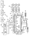
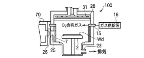
図1は、本発明の第1の実施形態に係る処理室のクリーニング方法が実施されるプラズマ処理装置の一例を模式的に示す断面図である。Embodiments of the present invention will be specifically described below with reference to the accompanying drawings.
FIG. 1 is a cross-sectional view schematically showing an example of a plasma processing apparatus in which the processing chamber cleaning method according to the first embodiment of the present invention is performed.
このマイクロ波プラズマ処理装置100は、所定のパターンで複数のスロットが形成された平面アンテナであるRLSA(Radial Line Slot Antenna)を利用してマイクロ波発生源から導かれたマイクロ波をチャンバー内に放射し、プラズマを形成するRLSAマイクロ波プラズマ処理装置として構成されており、例えば、ゲート電極のポリシリコンの側壁を選択酸化する処理に用いられる。
This microwave
このプラズマ処理装置100は、気密に構成され、接地された略円筒状のチャンバー1を有している。チャンバー1の底壁1aの略中央部には円形の開口部10が形成されており、底壁1aにはこの開口部10と連通し、下方に向けて突出する排気室11が設けられている。チャンバー1内には被処理基板であるウエハWやダミーウエハWdを水平に支持するためのAlN等のセラミックスからなるサセプタ2が設けられている。このサセプタ2は、排気室11の底部中央から上方に延びる円筒状のAlN等のセラミックスからなる支持部材3により支持されている。サセプタ2の外縁部にはウエハWをガイドするためのガイドリング4が設けられている。また、サセプタ2には抵抗加熱型のヒータ5が埋め込まれており、このヒータ5はヒータ電源6から給電されることによりサセプタ2を加熱して、その熱で被処理体であるウエハWを加熱する。このとき、例えば室温から800℃までの範囲で温度制御可能となっている。なお、チャンバー1の内周には、誘電体、例えば石英からなる円筒状のライナー7が設けられている。
The
サセプタ2には、ウエハWを支持して昇降させるためのウエハ支持ピン(図示せず)がサセプタ2の表面に対して突没可能に設けられている。
The
チャンバー1の側壁には環状をなすガス導入部材15が設けられており、このガス導入部材15にはガス供給系16が接続されている。ガス導入部材はシャワー状に配置してもよい。このガス供給系16は、Arガス供給源17、H2ガス供給源18、O2ガス供給源19を有しており、これらガスが、それぞれガスライン20を介してガス導入部材15に至り、ガス導入部材15からチャンバー1内に導入される。なお、ガスライン20の各々には、マスフローコントローラ21およびその前後の開閉バルブ22が設けられている。An annular
上記排気室11の側面には排気管23が接続されており、この排気管23には高速真空ポンプを含む排気装置24が接続されている。そしてこの排気装置24を作動させることによりチャンバー1内のガスが、排気室11の空間11a内へ均一に排出され、排気管23を介して排気される。これによりチャンバー1内は所定の真空度、例えば0.133Paまで高速に減圧することが可能となっている。
An
チャンバー1の側壁には、プラズマ処理装置100に隣接する搬送室(図示せず)との間でウエハWや、ダミーウエハWdの搬入出を行うための搬入出口25と、この搬入出口25を開閉するゲートバルブ26とが設けられている。
On the side wall of the
チャンバー1の上部は開口部となっており、この開口部の周縁部に沿って突出する環状の支持部27が設けられており、この支持部27に誘電体、例えば石英やAl2O3等のセラミックスからなり、マイクロ波を透過するマイクロ波透過板28がシール部材29を介して気密に設けられている。したがって、チャンバー1内は気密に保持される。The upper part of the
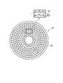
マイクロ波透過板28の上方には、サセプタ2と対向するように、円板状の平面アンテナ部材31が設けられている。この平面アンテナ部材31は支持部27の上端に係止されている。平面アンテナ部材31は、導体、例えば表面が金メッキされた銅板またはアルミニウム板からなり、複数のマイクロ波放射孔(スロット)32が所定のパターンで貫通して形成された構成となっている。このマイクロ波放射孔32は、例えば図2に示すように長溝状をなし、隣接するマイクロ波放射孔32同士が交差するように、典型的には図示のように直交するように(「T」字状に)配置され、これら複数のマイクロ波放射孔32が同心円状に配置されている。すなわち、平面アンテナ部材31はRLSAアンテナを構成している。マイクロ波放射孔32の長さや配列間隔は、マイクロ波の波長等に応じて決定される。また、マイクロ波放射孔32は、円形状、円弧状等の他の形状であってもよい。さらに、マイクロ波放射孔32の配置形態は特に限定されず同心円状の他、例えば、螺旋状、放射状に配置することもできる。
A disk-shaped
この平面アンテナ部材31の上面には、真空よりも大きい誘電率を有する誘電体からなる遅波材33が設けられている。
On the upper surface of the
チャンバー1の上面には、これら平面アンテナ部材31および遅波材33を覆うように、例えばアルミニウムやステンレス鋼等の金属材からなるシールド蓋体34が設けられている。チャンバー1の上面とシールド蓋体34とはシール部材35によりシールされている。シールド蓋体34には、冷却水流路34aが形成されている。なお、シールド蓋体34は接地されている。
A
シールド蓋体34の上壁の中央には開口部36が形成されており、この開口部には導波管37が接続されている。この導波管37の端部には、マッチング回路38を介してマイクロ波発生装置39が接続されている。これにより、マイクロ波発生装置39で発生した例えば周波数2.45GHzのマイクロ波が導波管37を介して上記平面アンテナ部材31へ伝搬されるようになっている。なお、マイクロ波の周波数としては、8.35GHz、1.98GHz等を用いることもできる。
An
導波管37は、上記シールド蓋体34の開口部36から上方へ延出する断面円形状の同軸導波管37aと、水平方向に延びる断面矩形状の矩形導波管37bとを有している。これらの間にはモード変換器40が設けられている。同軸導波管37aの中心には内導体41が延在しており、その下端部は、平面アンテナ部材31の中心に接続固定されている。
The
プラズマ処理装置100の各構成部は、プロセスコントローラ50に接続されて制御される構成となっている。プロセスコントローラ50には、工程管理者がプラズマ処理装置100を管理するためにコマンドの入力操作等を行うキーボードや、プラズマ処理装置100の稼働状況を可視化して表示するディスプレイ等からなるユーザーインターフェース51が接続されている。
Each component of the
また、プロセスコントローラ50には、プラズマ処理装置100で実行される各種処理をプロセスコントローラ50の制御にて実現するための制御プログラムや、処理条件に応じてプラズマエッチング装置の各構成部に処理を実行させるためのプログラムすなわちレシピが格納された記憶部52が接続されている。レシピはハードディスクや半導体メモリーに記憶されていてもよいし、CDROM、DVD等の可搬性の記憶媒体に収容された状態で記憶部52の所定位置にセットするようになっていてもよい。さらに、他の装置から、例えば専用回線を介してレシピを適宜伝送させるようにしてもよい
Further, the
そして、必要に応じて、ユーザーインターフェース51からの指示等にて任意のレシピを記憶部52から呼び出してプロセスコントローラ50に実行させることで、プロセスコントローラ50の制御下で、プラズマ処理装置100での所望の処理が行われる。
Then, if necessary, an arbitrary recipe is called from the
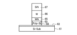
このように構成されたプラズマ処理装置100においては、上述したように、ゲート電極の選択酸化処理が行われる。ゲート電極は、従来、図3Aに示すように、Si基板61上にゲート絶縁膜62を介してポリシリコン膜63を形成したものが用いられてきたが、LSIの高集積化、高速化にともなうデザインルールの微細化の要請から、ゲート電極の低抵抗化が求められており、図3Bに示すような、Si基板61上にゲート絶縁膜62を介してポリシリコン膜63を形成し、さらにその上にタングステンシリサイド(WSi)64を形成したタングステンポリサイド構造や、図3Cに示すような、Si基板61上にゲート絶縁膜62を介してポリシリコン膜63を形成し、さらにタングステンナイトライド(WN)膜65、およびタングステン(W)膜66を形成した、より抵抗の低いタングステンポリメタルゲート構造等、タングステン(W)を用いたゲートが用いられている。したがって、ポリシリコンのみを酸化する選択酸化が必要となる。なお、図3A〜3Cにおいて、符号67はゲート電極をエッチングする際に用いられた、例えばSiN絶縁膜からなるハードマスク層、68は選択酸化により形成された酸化膜である。
In the
これらのうち、図3Cのタングステンポリメタルゲート電極を例にとってその製造工程を説明すると、まず、Si基板61上に例えば熱酸化等によりゲート絶縁膜62を形成し、その上にCVDによりポリシリコン膜63、タングステンナイトライド(WN)膜65、タングステン(W)膜66、ハードマスク層67を順次成膜し、その上にフォトレジスト膜(図示せず)を形成した後、フォトリソグラフィーによりフォトレジスト膜をマスクとしてハードマスク層67をエッチングし、さらにフォトレジスト膜+ハードマスク層67またはハードマスク層67をマスクとしてタングステン(W)膜66、タングステンナイトライド(WN)膜65、ポリシリコン膜63を順次エッチングしてゲート電極構造を形成し、その後、以下の条件で選択酸化処理を行ってポリシリコン膜63の側壁に酸化膜68を形成し、図3Cの構造を得る。
Of these, the manufacturing process will be described taking the tungsten polymetal gate electrode of FIG. 3C as an example. First, a
プラズマ処理装置100によりゲート電極の選択酸化処理を行う際には、まず、ゲートバルブ26を開にして搬入出口25からゲート電極が形成されたウエハWをチャンバー1内に搬入し、サセプタ2上に載置する。
When performing selective oxidation of the gate electrode by the
そして、ガス供給系16のArガス供給源17、H2ガス供給源18、およびO2ガス供給源19から、Arガス、H2ガス、およびO2ガスを所定の流量でガス導入部材15を介してチャンバー1内に導入し、所定の圧力に維持する。この際の条件としては、例えばガス流量を、Arガス:1000mL/min、H2ガス:200mL/min、O2ガス:100mL/minと高H2ガス濃度の条件とし、チャンバー内圧力を3〜700Pa、例えば6.7Pa(50mTorr)とする。Then, Ar
次いで、マイクロ波発生装置39からのマイクロ波をマッチング回路38を経て導波管37に導く。マイクロ波は、矩形導波管37b、モード変換器40、および同軸導波管37aを順次通って平面アンテナ部材31に供給され、平面アンテナ部材31からマイクロ波透過板28を経てチャンバー1内におけるウエハWの上方空間に放射される。
Next, the microwave from the
平面アンテナ部材31からマイクロ波透過板28を経てチャンバー1に放射されたマイクロ波によりチャンバー1内ではH2ガス、Arガス、およびO2ガスがプラズマ化し、このプラズマによりウエハWのゲート電極のポリシリコン側壁を選択酸化する。このマイクロ波プラズマは、略1011/cm3以上のプラズマ密度でかつ略0.5〜2eVの低電子温度プラズマであり、低温かつ短時間で選択酸化処理を行って薄い酸化膜を形成することができ、しかも下地膜へのイオン等のプラズマダメージが小さい等のメリットがある。また、図3B、図3Cに示すようなタングステン(W)を含むゲート電極の場合に、このように高密度プラズマにより低温、短時間で、かつ高H2/O2のガス配合でポリシリコンの選択酸化処理を行うので、タングステン(W)の酸化によるWOx(WO3、WO2、またはWO)の昇華を極力抑えて極めて高精度の処理を行うことができる。In the
しかしながら、WOxの昇華は完全には防止することができず、昇華したWOxによってチャンバー1内が汚染される。このような状態のチャンバー1で次のウエハに対して選択酸化処理を行う場合には、チャンバー1に付着したタングステン(W)が処理に悪影響を与えタングステン(W)がコンタミネーションとして素子に取り込まれるおそれがある他、タングステン(W)によって酸化処理が妨げられてしまう。したがって、選択酸化処理後のチャンバー1はクリーニングによりタングステン(W)の汚染レベルを例えば1011atoms/cm2オーダーまたはそれ以下、好ましくは1010atoms/cm2オーダー以下のレベルまで清浄化する必要がある。汚染レベルは低いほど良い。However, the sublimation of WO x cannot be completely prevented, and the inside of the
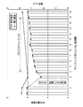
本実施形態においては、上述のようなWを含有するゲート電極のポリシリコン側壁の選択酸化処理を行った後、Wによって汚染されたチャンバー1を大気開放することなく、プラズマによるドライクリーニングを実施する。以下、このクリーニング処理について図4A〜4Dを参照しながら説明する。
In this embodiment, after performing the selective oxidation treatment of the polysilicon side wall of the gate electrode containing W as described above, dry cleaning by plasma is performed without opening the
選択酸化処理後、まず、図4Aに示すように、大気開放することなく、ゲートバルブ26を開にして減圧状態に保持された搬送室70から搬入出口25を介して搬送装置71により、清浄なダミーウエハWdをチャンバー1内に搬入し、サセプタ2上に載置する。これはダミーウエハWdにて、サセプタ2をプラズマから保護するため、およびチャンバー1のクリーニング後にダミーウエハWdの表面を観察して汚染状態の改善度合いを評価するために行われる。なお、この工程は必須のものではなく、サセプタ2のダメージを考慮する必要がない場合にはダミーウエハWdは載置しなくてもよい。
After the selective oxidation treatment, first, as shown in FIG. 4A, the cleaning is performed by the
次に、図4Bに示すように、チャンバー1内を排気しつつガス供給系16からO2を含むガスをチャンバー1内に導入する。そして、図4Cに示すように、上記ポリシリコン側壁の選択酸化処理の際と同様、マイクロ波発生装置39からのマイクロ波をチャンバー1内に導き、O2を含むガスをプラズマ化する。すなわち、マイクロ波発生装置39からのマイクロ波は、マッチング回路38を経て導波管37に導かれ、矩形導波管37b、モード変換器40、および同軸導波管37a、遅波材33を順次通って平面アンテナ部材31に供給され、平面アンテナ部材31のスロットからマイクロ波透過板28を経てチャンバー1内に放射され、このマイクロ波によりチャンバー1内に導入されたO2を含むガスがプラズマ化する。その際に、図4Dに示すように、このプラズマにより、基本的にチャンバー1に付着したWOxは昇華し、排気管23を介して排気され、これにより、チャンバー1内が清浄化される。この際に、処理ガス中にH2が含まれていると、WOxが還元されて、イオンなどのより不安定な状態となっていっそう昇華しやすくなるものと推測される。このようなクリーニング処理は、1枚のデバイスウエハの選択酸化処理が終了する毎に行うことが好ましい。また、選択酸化処理に先立って、クリーニング処理と同様の条件でシーズニング処理を行うことが好ましい。もちろん、デバイスウエハを複数枚処理した後にクリーニングするようにしてもよい。Next, as shown in FIG. 4B, a gas containing O 2 is introduced into the
このようなクリーニング処理において、チャンバー1内の圧力は、例えば3〜1333Paに設定される。この中では3〜67Paが好ましく、例えば6.7Paが例示される。また、チャンバー1内の温度(例えばサセプタ2の温度)は、45℃以上が好ましい。この際にサセプタ2の温度は高い方がよく、200〜800℃が好ましく、400〜800℃が特に好ましい。さらに、マイクロ波発生装置39のパワーは1.0〜5.0kWが好ましい。
In such a cleaning process, the pressure in the
導入するO2を含むガスは、O2ガス単独でもよいが、好ましくはO2ガス+Arガスであり、さらに好ましくはO2ガス+H2ガス+Arガスである。O2ガス単独の場合には、その流量は50〜1000mL/minが好ましく、特に、100〜500mL/min程度が好ましい。O2ガスの流量が多くなりすぎるとプラズマ密度が低下するため、クリーニング効果が低下してしまう。また、O2ガスとArガスのプラズマの場合には、これらの流量を適切に調整することにより、O2ガス単独の場合よりもクリーニング効果を高めることができる。これは、Arガスが入ることにより、プラズマ密度が高くなるためであると思われる。この場合の流量は、O2ガス:10〜500mL/min、Arガス:200〜2000mL/minが好ましい。そして、さらにH2ガスを適量加えたプラズマの場合は、クリーニング効果を一層高めることができる。O2ガス+H2ガス+Arガスの場合の流量は、O2ガス:10〜500mL/min、Arガス:200〜2000mL/min、H2ガス10〜500mL/minが好ましい。O2ガスに対するH2ガスの流量比が2以上でクリーニング効果を高めることができ、4以上がより好ましく、さらには6以上である。The gas containing O 2 to be introduced may be O 2 gas alone, but is preferably O 2 gas + Ar gas, and more preferably O 2 gas + H 2 gas + Ar gas. In the case of O 2 gas alone, the flow rate is preferably 50 to 1000 mL / min, particularly preferably about 100 to 500 mL / min. If the flow rate of the O 2 gas is excessively increased, the plasma density is lowered, so that the cleaning effect is lowered. Further, in the case of plasma of O 2 gas and Ar gas, the cleaning effect can be enhanced as compared with the case of O 2 gas alone by appropriately adjusting these flow rates. This is presumably because the plasma density increases when Ar gas enters. The flow rates in this case are preferably O 2 gas: 10 to 500 mL / min, Ar gas: 200 to 2000 mL / min. Further, in the case of plasma in which an appropriate amount of H 2 gas is added, the cleaning effect can be further enhanced. The flow rates in the case of O 2 gas + H 2 gas + Ar gas are preferably O 2 gas: 10 to 500 mL / min, Ar gas: 200 to 2000 mL / min, and H 2 gas 10 to 500 mL / min. O 2 flow rate ratio of the H 2 gas to the gas it is possible to enhance the cleaning effect at 2 or more, more preferably 4 or more, or even 6 or more.
また、O2ガス+Arガスと、O2ガス+H2ガス+Arガスとを交互に繰り返す、例えばO2ガス+ArガスにH2ガスを間欠的に添加することにより、クリーニング効果をさらに高めることができる。また、クリーニングガスの供給と、真空引きあるいはパージガスを導入しながらの真空引きとを交互に繰り返すことでさらに効果を高めることができる。Further, the cleaning effect can be further enhanced by alternately repeating O 2 gas + Ar gas and O 2 gas + H 2 gas + Ar gas, for example, by intermittently adding H 2 gas to O 2 gas + Ar gas. . Further, the effect can be further enhanced by alternately repeating the supply of the cleaning gas and the evacuation while evacuating or introducing the purge gas.
さらに、図1の装置にHeガスまたはNeガスをチャンバー1内に導入するラインを設け、クリーニング条件のプラズマを生成する直前に、チャンバー内にHeガスまたはNeガスのプラズマを生成させることが好ましい。これにより、チャンバー1壁の表面温度をプラズマ加熱で上昇させておくことができ、WOxを一層昇華させやすくなるため、クリーニング効率が上昇する。Further, it is preferable that a line for introducing He gas or Ne gas into the
このように、本実施形態によれば、チャンバー1を大気開放することなく、プラズマによりクリーニングしてチャンバー壁のW成分を除去することができるので、チャンバーを大気開放する時間、ウェット洗浄する時間、再排気する時間、および排気後の処理チャンバーを再コンデショニングする時間等が必要であった従来のウェットクリーニング処理に比較してクリーニング時間を著しく短縮することができる。一例を挙げれば、従来少なくとも2時間必要であったものを、2〜30分にすることができる。
As described above, according to the present embodiment, the
このようにしてクリーニング処理した後、上述した選択酸化処理のようなプラズマ処理が実施される。これにより、W汚染レベルが極めて低い清浄な状態でプラズマ処理を行うことができ、Wコンタミネーションによる選択酸化処理の阻害等の不都合が生じない。 After the cleaning process is performed in this manner, a plasma process such as the selective oxidation process described above is performed. As a result, the plasma treatment can be performed in a clean state with a very low W contamination level, and there is no inconvenience such as inhibition of the selective oxidation treatment due to W contamination.
次に、本実施形態の効果を確認した実験について説明する。
まず、クリーニングのガス種および流量を変化させてクリーニング効果を確認した。この実験では、図1の装置を用い、最初にW汚染のないチャンバーに全面にW膜が形成されたSiウエハ(200mm)1枚をチャンバーに搬入し、クリーニング処理を模擬して、O2ガス単独、O2ガス+Arガス、O2ガス+H2ガス+Arガスを用い、流量を種々変化させてチャンバーに導入するとともに、マイクロ波発生装置のパワーを3.4kWとしてマイクロ波をチャンバーに導入し、ウエハ温度400℃でプラズマを180秒間生成した。チャンバー壁温度は45℃であった。Next, an experiment for confirming the effect of the present embodiment will be described.
First, the cleaning effect was confirmed by changing the cleaning gas type and flow rate. In this experiment, using the apparatus shown in FIG. 1, first, an Si wafer (200 mm) having a W film formed on the entire surface is carried into a chamber free of W contamination, and a cleaning process is simulated to simulate O 2 gas. Alone, using O 2 gas + Ar gas, O 2 gas + H 2 gas + Ar gas, and introducing into the chamber at various flow rates, introducing the microwave into the chamber with a microwave generator power of 3.4 kW, Plasma was generated at a wafer temperature of 400 ° C. for 180 seconds. The chamber wall temperature was 45 ° C.
次いで、W膜が形成されたSiウエハを搬出し、清浄なベアSiウエハを搬入し、ポリシリコンの選択酸化条件と同様の条件にてプラズマ処理を行った。すなわち、ガス流量:Ar/H2/O2=1000/200/100mL/minとし、チャンバー内圧力:6.7Pa、マイクロ波発生装置のパワー:3.4kW、サセプタ温度:400℃、処理時間:110秒とした。Next, the Si wafer on which the W film was formed was unloaded, a clean bare Si wafer was loaded, and plasma treatment was performed under the same conditions as the selective oxidation conditions for polysilicon. That is, the gas flow rate: Ar / H 2 / O 2 = 1000/200/100 mL / min, the pressure in the chamber: 6.7 Pa, the power of the microwave generator: 3.4 kW, the susceptor temperature: 400 ° C., the processing time: 110 seconds.
この処理の後、ベアSiウエハを搬出し、その表面のW汚染量をTXRF(Total
Reflection X-Ray Fluorescence:全反射蛍光X線分析)により計測した。このW汚染量は上述のクリーニング条件によってW付きウエハから取り去られたW量と強い相関があると考えられ、取り去られたW量が多いほどクリーニング効果が大きいと判断できるため、このW汚染量によってクリーニング効果の大小を判断した。結果を図5に示す。After this treatment, the bare Si wafer is unloaded, and the amount of W contamination on the surface is measured by TXRF (Total
Reflection X-Ray Fluorescence (total reflection fluorescent X-ray analysis). The amount of W contamination is considered to have a strong correlation with the amount of W removed from the wafer with W due to the cleaning conditions described above, and it can be determined that the larger the amount of W removed, the greater the cleaning effect. The magnitude of the cleaning effect was judged by the amount. The results are shown in FIG.
図5に示すように、O2ガス単独の場合、流量を100、300、500mL/minで変化させたが、これらの中で、300mL/minが最もクリーニング効果が高かった。これは、O2ガスが多すぎるとプラズマ密度が低下しWOxの生成率が低くなるためであると考えられる。O2ガスとArガスの両方を供給した場合(Ar/O2=1000/100mL/min)には、ベアSiウエハのW濃度が増加し、O2ガス単独の場合に比較してクリーニング効果が上昇することが確認された。As shown in FIG. 5, in the case of O 2 gas alone, the flow rate was changed at 100, 300, and 500 mL / min, but among these, 300 mL / min had the highest cleaning effect. This is considered to be because if the O 2 gas is too much, the plasma density is lowered and the production rate of WO x is lowered. When both O 2 gas and Ar gas are supplied (Ar / O 2 = 1000/100 mL / min), the W concentration of the bare Si wafer increases, and the cleaning effect is improved as compared with the case of O 2 gas alone. It was confirmed to rise.
次に、実際のクリーニングテストを行った。
ここでは、図1の構造の装置を用い、まず、チャンバーをクリーニングし、Wフリーの状態とした。次いで、次の酸化処理と同じ条件でチャンバー内のシーズニングを行った。シーズニングは、チャンバー内において酸素プラズマ形成と真空引きとを少なくとも1サイクル実施することにより行った。Next, an actual cleaning test was performed.
Here, the apparatus having the structure of FIG. 1 was used, and the chamber was first cleaned to be in a W-free state. Next, seasoning in the chamber was performed under the same conditions as in the next oxidation treatment. Seasoning was performed by performing at least one cycle of oxygen plasma formation and evacuation in the chamber.
その後、1枚目のサンプリング用のベアSiウエハをサセプタ上に載せ、ポリシリコンの選択酸化処理と同様の条件で酸化処理を行った。その際の条件は、ガス流量:Ar/H2/O2=1000/200/100mL/minとし、チャンバー内圧力:6.7Pa、マイクロ波発生装置のパワー:3.4kW、ウエハ温度:400℃、チャンバー壁温度:45℃、処理時間:110秒として酸化膜の膜厚が8nmとなるように実施した。処理後、この1枚目のサンプリング用ウエハを取り出して表面のW濃度を測定した。その結果W濃度は検出限界の3×108atoms/cm2以下とWフリー(清浄)と確認された。なお、W濃度測定は、上述したTXRFを用いて行った(以下、同じ)。この値をチャンバーのリファレンスのW濃度とした。After that, the first bare Si wafer for sampling was placed on the susceptor, and oxidation treatment was performed under the same conditions as the selective oxidation treatment of polysilicon. The conditions at that time were as follows: gas flow rate: Ar / H 2 / O 2 = 1000/200/100 mL / min, pressure in the chamber: 6.7 Pa, power of the microwave generator: 3.4 kW, wafer temperature: 400 ° C. The chamber wall temperature was 45 ° C., the processing time was 110 seconds, and the film thickness of the oxide film was 8 nm. After the processing, the first sampling wafer was taken out and the surface W concentration was measured. As a result, the W concentration was 3 × 10 8 atoms / cm 2 or less, which was the detection limit, and was confirmed to be W-free (clean). Note that the W concentration measurement was performed using the above-described TXRF (hereinafter the same). This value was used as the W concentration of the reference of the chamber.
引き続き、表面にW膜を有するSiウエハをサセプタ上に載置し、処理時間を2分間にした以外は同様の条件で酸化処理を行いチャンバー内を汚染させた。なお、この時間はデバイスウエハ約5枚の処理時間に相当する。処理後、このW膜付きウエハを搬出し、2枚目のサンプリング用のベアSiウエハをサセプタ上に載置し、1枚目のウエハと同様の条件で酸化処理を行った。処理後、この2枚目のサンプリング用ウエハを取り出して表面のW濃度を測定した。その結果、ウエハ表面のW濃度は約4×10¹⁰atoms/cm2と高くなった。Subsequently, a Si wafer having a W film on the surface was placed on the susceptor, and the chamber was contaminated by oxidation treatment under the same conditions except that the treatment time was 2 minutes. This time corresponds to the processing time of about 5 device wafers. After the processing, this W film-coated wafer was unloaded, a second bare Si wafer for sampling was placed on the susceptor, and an oxidation process was performed under the same conditions as the first wafer. After the processing, the second sampling wafer was taken out and the surface W concentration was measured. As a result, the W concentration on the wafer surface was as high as about 4 × 10 10 atoms / cm 2 .
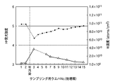
次いで、Ar/O2ガスによるプラズマクリーニングを行った。すなわち、ガス流量:Ar/O2=1000/300mL/min、チャンバー内圧力:6.7Pa、マイクロ波発生装置のパワー:3.4kW、サセプタ温度:400℃、処理時間:180秒の条件でクリーニング処理を行い、処理後、3枚目のサンプリング用のベアSiウエハをサセプタ上に載置し、1枚目のサンプリング用ウエハと同様の条件で酸化処理を行った。処理後、この3枚目のサンプリングウエハを取り出して表面のW濃度を測定した。その結果、ウエハ表面のW濃度は約1.3×1011atoms/cm2であった。以降、同様のクリーニング処理を行い、次いで1枚目のサンプリングウエハと同様の条件での酸化処理を行った後、W濃度測定する一連の操作を13枚目のサンプリング用ウエハまで合計11枚繰り返した。Next, plasma cleaning with Ar / O 2 gas was performed. That is, cleaning was performed under the conditions of gas flow rate: Ar / O 2 = 1000/300 mL / min, chamber pressure: 6.7 Pa, microwave generator power: 3.4 kW, susceptor temperature: 400 ° C., and processing time: 180 seconds. After the processing, a third sampling bare Si wafer was placed on the susceptor, and an oxidation process was performed under the same conditions as the first sampling wafer. After the treatment, the third sampling wafer was taken out and the surface W concentration was measured. As a result, the W concentration on the wafer surface was about 1.3 × 10 11 atoms / cm 2 . Thereafter, the same cleaning process was performed, and then the oxidation process was performed under the same conditions as the first sampling wafer. Then, a series of operations for measuring the W concentration were repeated for a total of 11 sheets up to the 13th sampling wafer. .
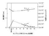
最後に、14枚目のサンプリング用のベアSiウエハをサセプタに載置し、1枚目のサンプリング用ウエハと同じ条件で酸化処理を行った後、この14枚目のサンプリング用ウエハを取り出して表面のW濃度を測定した。これら一連の実験の結果を図6に示す。 Finally, after the 14th sampling bare Si wafer is placed on the susceptor and oxidized under the same conditions as the 1st sampling wafer, this 14th sampling wafer is taken out and the surface is removed. The W concentration of was measured. The results of these series of experiments are shown in FIG.
図6は、横軸にウエハ番号(処理順番)をとり、縦軸にウエハ表面のW濃度をとって、本発明のクリーニングによる効果を示す図である。この図に示すように、本発明の範囲内の3分間のクリーニング処理がウエハ10枚分以内、すなわち30分間以内でW濃度が1×10¹⁰atoms/cm2以下となることが確認された。具体的には、21分以上、好ましくは27分以上でW濃度が1×1010atoms/cm2以下を達成可能であることが確認された。FIG. 6 is a diagram showing the effect of cleaning according to the present invention, with the wafer number (processing order) on the horizontal axis and the W concentration on the wafer surface on the vertical axis. As shown in this figure, it was confirmed that the cleaning process for 3 minutes within the range of the present invention is within 10 wafers, that is, within 30 minutes, the W concentration becomes 1 × 10 10 atoms / cm 2 or less. Specifically, it has been confirmed that the W concentration can be 1 × 10 10 atoms / cm 2 or less in 21 minutes or longer, preferably 27 minutes or longer.
また、各サンプリング用ウエハの選択酸化処理の際の酸化膜の厚さを測定した。この際の各サンプリングウエハにおける酸化膜厚を図7に示す。なお、図7には酸化膜厚の他、W濃度もプロットした。この図に示すように、1枚目のサンプリング用ウエハでは酸化膜の厚さが110秒の処理で7.99nmであったのに対し、2枚目ではWの汚染によりポリシリコンの酸化が妨げられて酸化膜の厚さが110秒で7.75nmと薄くなったが、チャンバー内がクリーニングされてW濃度が減少するにつれて酸化膜厚さが徐々に回復し、最後の14枚目のウエハにおける酸化膜の厚さは8.03nmであり、W汚染による酸化阻害が解消されていることが確認された。このことから理解されるように、W汚染量(W濃度)と酸化膜厚とは強い相関関係があり、酸化膜厚によってクリーニングの終点を把握することが可能である。 Further, the thickness of the oxide film during the selective oxidation treatment of each sampling wafer was measured. The oxide film thickness in each sampling wafer at this time is shown in FIG. FIG. 7 also plots the W concentration in addition to the oxide film thickness. As shown in this figure, the thickness of the oxide film in the first sampling wafer was 7.99 nm after 110 seconds of processing, whereas in the second wafer, the oxidation of polysilicon was hindered by W contamination. As a result, the thickness of the oxide film decreased to 7.75 nm in 110 seconds, but the oxide film thickness gradually recovered as the W concentration decreased as the inside of the chamber was cleaned. The thickness of the oxide film was 8.03 nm, and it was confirmed that the oxidation inhibition due to W contamination was eliminated. As understood from this, the amount of W contamination (W concentration) and the oxide film thickness have a strong correlation, and the end point of cleaning can be grasped by the oxide film thickness.
次に、条件を種々変化させて、実際のクリーニングテストを行った。
ここでは、図1の構造の装置を用い、上のテストと同様、まず、チャンバーをクリーニングし、Wフリーの状態とし、次いで、チャンバー内のシーズニングを行い、その後、1枚目のサンプリング用のベアSiウエハをサセプタ上に載せ、上記テストと同様に酸化処理を行った。処理後、この1枚目のウエハを取り出して表面のW濃度を測定し、W濃度は検出限界以下であることを確認した。Next, actual cleaning tests were performed under various conditions.
Here, as in the above test, using the apparatus having the structure shown in FIG. 1, the chamber is first cleaned to be in a W-free state, then seasoned in the chamber, and then the first sampling bare A Si wafer was placed on the susceptor and oxidation treatment was performed in the same manner as in the above test. After the processing, this first wafer was taken out and the W concentration on the surface was measured, and it was confirmed that the W concentration was below the detection limit.
引き続き、表面にW膜を有するSiウエハをサセプタ上に載せ、上のテストと同様の条件でデバイスウエハ約1ロット(25枚相当)に対応する10分間酸化処理を行いチャンバー内をWで汚染させた。W膜付きウエハを搬出し、2枚目のサンプリング用ベアSiウエハをサセプタ上に載置し、1枚目と同様の条件で酸化処理を行った。処理後、この2枚目のサンプリングウエハを取り出して表面のW濃度を測定した。その結果、ウエハ表面のW濃度は1012atoms/cm2オーダーと高い値となった。Subsequently, a Si wafer having a W film on the surface is placed on the susceptor, and oxidation is performed for 10 minutes corresponding to about one lot of device wafers (corresponding to 25 wafers) under the same conditions as in the above test to contaminate the chamber with W. It was. The wafer with the W film was carried out, a second sampling bare Si wafer was placed on the susceptor, and an oxidation treatment was performed under the same conditions as in the first sheet. After the processing, the second sampling wafer was taken out and the surface W concentration was measured. As a result, the W concentration on the wafer surface was as high as 10 12 atoms / cm 2 .
次いで、Ar/O2/H2ガスによるプラズマクリーニングを行った。すなわち、ガス流量の比率、チャンバー内圧力、チャンバー温度(サセプタ温度)を変化させ、処理時間180秒でクリーニング処理を行い、処理後、3枚目のサンプリング用のベアSiウエハをサセプタ状に載置し、1枚目のサンプリング用ウエハと同様の条件で酸化処理を行った。処理後、この3枚目のサンプリングウエハを取り出して表面のW濃度を測定した。同様のクリーニング処理を行い、次いで1枚目のサンプリングウエハと同様の条件での酸化処理を行った後、W濃度測定する一連の操作を13枚目のサンプリングウエハまで合計11枚繰り返した。Next, plasma cleaning with Ar / O 2 / H 2 gas was performed. That is, the ratio of gas flow rate, chamber pressure, and chamber temperature (susceptor temperature) are changed, cleaning processing is performed in a processing time of 180 seconds, and a third bare silicon wafer for sampling is placed in a susceptor shape after processing. Then, oxidation treatment was performed under the same conditions as those for the first sampling wafer. After the treatment, the third sampling wafer was taken out and the surface W concentration was measured. A similar cleaning process was performed, followed by an oxidation process under the same conditions as the first sampling wafer, and then a series of operations for measuring the W concentration were repeated for a total of 11 sheets up to the 13th sampling wafer.
最後に、14枚目のサンプリング用のベアSiウエハをサセプタに載置し、1枚目のウエハと同じ条件で酸化処理を行った後、この14枚目のウエハを取り出して表面のW濃度を測定した。 Finally, the 14th bare silicon wafer for sampling is placed on the susceptor, and the oxidation process is performed under the same conditions as the first wafer. Then, the 14th wafer is taken out and the W concentration on the surface is reduced. It was measured.
この際に、クリーニング処理の条件として、サセプタ温度を400℃、チャンバー内圧力を6.7Paとし、H2/O2比を0(Ar/O2/H2=1000:300:0mL/min),8(Ar/O2/H2=1000:50:400mL/min),10(Ar/O2/H2=700:50:500mL/min)と変化させて、上記クリーニング処理を行い、その後酸化処理を行ってサンプリング用ウエハ表面のW濃度を測定した。その結果を図8に示す。At this time, the cleaning process conditions were a susceptor temperature of 400 ° C., a chamber pressure of 6.7 Pa, and an H 2 / O 2 ratio of 0 (Ar / O 2 / H 2 = 1000: 300: 0 mL / min). , 8 (Ar / O 2 / H 2 = 1000: 50: 400 mL / min), 10 (Ar / O 2 / H 2 = 700: 50: 500 mL / min) Oxidation treatment was performed to measure the W concentration on the sampling wafer surface. The result is shown in FIG.
図8に示すように、W濃度の測定値は、O2ガスに対するH2ガスの流量比(H2/O2比)が10までは、流量比の増加にともなって低下する傾向があり、その値が2以上で比較的良好なクリーニング効果が得られる。そして、H2/O2比が8で最もW濃度が低くなり、それを超えてもクリーニング効果が飽和する。このことからH2/O2比が4以上がより好ましく、6以上がさらに好ましいことが確認された。As shown in FIG. 8, the measured value of the W concentration tends to decrease as the flow rate ratio increases until the flow rate ratio of the H 2 gas to the O 2 gas (H 2 / O 2 ratio) is up to 10. When the value is 2 or more, a relatively good cleaning effect can be obtained. The W concentration is lowest when the H 2 / O 2 ratio is 8, and the cleaning effect is saturated even when the H concentration exceeds 8. From this, it was confirmed that the H 2 / O 2 ratio is more preferably 4 or more, and more preferably 6 or more.
次に、サセプタ温度を400℃、ガス組成をAr/O2/H2=1000:50:400mL/minとし、チャンバー内圧力を6.7Paにした場合と126Paにした場合とで上記クリーニング処理を行い、その後酸化処理を行ってサンプリング用ウエハ表面のW濃度を測定した。その結果を図9に示す。Next, the above susceptor temperature is 400 ° C., the gas composition is Ar / O 2 / H 2 = 1000: 50: 400 mL / min, and the above-described cleaning treatment is performed when the chamber internal pressure is 6.7 Pa and 126 Pa. After that, oxidation treatment was performed to measure the W concentration on the surface of the sampling wafer. The result is shown in FIG.
図9に示すように、チャンバー内圧力が低い6.7Paのほうが126PaよりもW濃度の測定値が低い結果となった。このことから、チャンバー内圧力が低いほどクリーニング効果が高いことが確認された。これは、W化合物の蒸気圧が高くなっているからと考えられる。 As shown in FIG. 9, the measured value of W concentration was lower at 6.7 Pa where the pressure in the chamber was lower than at 126 Pa. From this, it was confirmed that the lower the pressure in the chamber, the higher the cleaning effect. This is presumably because the vapor pressure of the W compound is high.
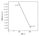
次に、ガス組成をAr/O2/H2=1000:50:400mL/min、チャンバー内圧力を6.7Paとし、サセプタ温度を400℃にした場合と600℃にした場合とで上記クリーニング処理を行い、表面のW濃度を測定した。その結果を図10に示す。Next, the above cleaning treatment is performed when the gas composition is Ar / O 2 / H 2 = 1000: 50: 400 mL / min, the pressure in the chamber is 6.7 Pa, and the susceptor temperature is 400 ° C. and 600 ° C. The W concentration on the surface was measured. The result is shown in FIG.
図10に示すように、サセプタ温度が高いほうがW濃度の測定値が低く、600℃の場合に、W濃度が3.6×10¹⁰atoms/cm2と採用した条件の中では最も低くなった。これも、上記圧力を変化させた場合と同様、W化合物の蒸気圧が上昇したためであると考えられる。As shown in FIG. 10, the measured value of the W concentration is lower when the susceptor temperature is higher, and when the temperature is 600 ° C., the W concentration is the lowest among the conditions adopted as 3.6 × 10 10 atoms / cm 2 . . This is also considered to be due to an increase in the vapor pressure of the W compound as in the case where the pressure was changed.
また、この際の14枚目のウエハにおける酸化膜の厚さは、ほぼ初期値と同等の8.1nmであり、W汚染による酸化阻害が生じていないことが確認された。 In addition, the thickness of the oxide film on the 14th wafer at this time was 8.1 nm, which is substantially equal to the initial value, and it was confirmed that no oxidation inhibition due to W contamination occurred.
次に、本発明の第2の実施形態について説明する。
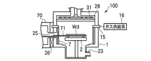
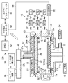
図11は、本発明の第2の実施形態に係る処理室のクリーニング方法が実施されるプラズマ処理装置の一例を模式的に示す断面図である。Next, a second embodiment of the present invention will be described.
FIG. 11 is a cross-sectional view schematically showing an example of a plasma processing apparatus in which the processing chamber cleaning method according to the second embodiment of the present invention is performed.
このプラズマ処理装置200は、前記図1のプラズマ処理装置に終点検出機能が付加されたものであり、図11において図1と同一のものには同一の符号を付して説明を省略する。
The
このプラズマ処理装置200においては、チャンバー1の側壁の下部に、クリーニングの終点検出の際に利用される透光性の窓80が設けられている。この窓80に隣接して受光部81が配備され、受光部81はプラズマの発光強度を測定するためのモノクロメータなどの分光制御計82と電気的に接続されている。窓80を設けた位置は、平面アンテナ部材31から離れているためプラズマの影響を受けにくく、また排気経路にもなっていないため、窓80への付着物が少なく、安定して測定を行なうことができる。なお、分光制御計82の設置位置は特に限定されず、安定して測定可能な位置であればどの位置でもよい。また、チャンバー1内には、石英からなる円筒状のライナー7が設けられているので、窓80とライナー7を通してプラズマ中のラジカルの発光強度を測定可能である。ライナー7に開口を設けることは可能であるが、窓80への付着物防止の観点からはむしろ開口を設けないことが好ましい。
In this
プロセスコントローラ50は、接続配線53によって分光制御計82と電気的に接続されており、上記機能の他、分光制御計82で検出されたH*ラジカル等の発光強度の情報を解析し、クリーニングの終点判断を行なう。そして、プロセスコントローラ50の指示により、例えばクリーニングを自動停止したり、クリーニングが終了した旨をユーザーインターフェース51のディスプレイに表示したりする。The
このように構成されたプラズマ処理装置200においては、第1の実施形態と同様に、ゲート電極の選択酸化処理が行われ、その後、WOxの昇華により汚染されたチャンバー1を大気開放することなく、プラズマによるドライクリーニングを実施する。なお、本実施形態の場合には、クリーニングガスとして水素含有ガスが必須である。In the
具体的には、上述の図4A〜4Dに従ってクリーニング処理を実施する。選択酸化処理後、まず、図4Aに示すように、大気開放することなく、ゲートバルブ26を開にして減圧状態に保持された搬送室70から搬入出口25を介して搬送装置71により、必要に応じて清浄なダミーウエハWdをチャンバー1内に搬入し、サセプタ2上に載置する。その後、図4Bに示すように、チャンバー1内を排気しつつガス供給系16からAr/H2/O2からなるクリーニングガスをチャンバー1内に導入する。そして、図4Cに示すように、上記ポリシリコン側壁の選択酸化処理の際と同様、マイクロ波発生装置39からのマイクロ波をチャンバー1内に導き、クリーニングガスをプラズマ化する。その際に、図4Dに示すように、このプラズマにより、第1の実施形態と同様にして、チャンバー1内が清浄化される。Specifically, the cleaning process is performed according to the above-described FIGS. After the selective oxidation treatment, first, as shown in FIG. 4A, it is necessary to open the
このようなクリーニング処理において、チャンバー1内の圧力は、例えば3〜1333Paに設定される。また、チャンバー1内の温度(例えば、チャンバー壁やサセプタ2の温度)は、45℃以上が好ましい。この際、サセプタ2の温度は高い方がよく、略400〜800℃がより好ましい。また、クリーニング中は、連続的にチャンバー1の排気を行なってもよいが、間欠的に排気を行なうようにすることが好ましい。また、排気の際にパージガスを流しても効果がある。
In such a cleaning process, the pressure in the
導入するクリーニングガスは、例えば、H2ガス+Arガスでもよいが、O2ガス+H2ガス+Arガスが好ましい。H2ガスを適量加えることにより、クリーニング効果を高めることができる。O2ガス+H2ガス+Arガスの場合の流量は、O2ガス:10〜500mL/min、Arガス:200〜2000mL/min、H2ガス:40〜2000mL/minが好ましい。O2ガスに対するH2ガスの流量比が2以上でクリーニング効果を高めることができ、4以上がより好ましく、さらには6以上である。また、O2ガス+Arガスと、O2ガス+H2ガス+Arガスとを交互に繰り返す、すなわちO2ガス+ArガスにH2ガスを間欠的に添加することにより、クリーニング効果をさらに高めることができる。また、クリーニングガスの供給と、真空引きあるいはパージガスを導入しながらの真空引きとを交互に繰り返すことでさらに効果を高めることができる。さらに、図11の装置にHeガスまたはNeガスをチャンバー1内に導入するラインを設け、クリーニング条件のプラズマを生成する直前に、チャンバー内にHeガスまたはNeガスのプラズマを生成させることが好ましい。これにより、チャンバー1壁の表面温度をプラズマ加熱で上昇させておくことができ、WOxを一層昇華させやすくなるため、クリーニング効率が上昇する。さらに、マイクロ波発生装置39のパワーは1.0〜5.0kWが好ましい。The introduced cleaning gas may be, for example, H 2 gas + Ar gas, but O 2 gas + H 2 gas + Ar gas is preferable. The cleaning effect can be enhanced by adding an appropriate amount of H 2 gas. The flow rates in the case of O 2 gas + H 2 gas + Ar gas are preferably O 2 gas: 10 to 500 mL / min, Ar gas: 200 to 2000 mL / min, and H 2 gas: 40 to 2000 mL / min. O 2 flow rate ratio of the H 2 gas to the gas it is possible to enhance the cleaning effect at 2 or more, more preferably 4 or more, or even 6 or more. Further, the cleaning effect can be further enhanced by alternately repeating O 2 gas + Ar gas and O 2 gas + H 2 gas + Ar gas, that is, intermittently adding H 2 gas to O 2 gas + Ar gas. . Further, the effect can be further enhanced by alternately repeating the supply of the cleaning gas and the evacuation while evacuating or introducing the purge gas. Furthermore, it is preferable to provide a line for introducing He gas or Ne gas into the
クリーニング中は、チャンバー1内のプラズマ中のラジカルの発光強度を分光制御計82によって測定する。分光制御計82では、受光部81で検知したプラズマの発光がスペクトルに分けられる。分光制御計82により測定されるラジカルの発光スペクトルの中から、クリーニングの進行に伴って増加するラジカル、例えば水素ラジカルH*の波長656nmの発光強度を測定し、モニターする。本実施形態では、H*の発光強度が、ほぼ初期状態(Wによる汚染前の状態)まで回復した時点を以てクリーニングの終点を知ることができる。また、クリーニングの終点は、H*の発光強度を経時的にグラフ化し、その変化率(例えば発光強度のグラフの接線の傾き)から判定することもできる。During cleaning, the emission intensity of radicals in the plasma in the
水素ラジカルの発光強度によりクリーニングの終点検出が可能となるメカニズムは未だ明らかではないが、以下のように考えれば合理的な説明が可能となる。 The mechanism that makes it possible to detect the end point of cleaning based on the emission intensity of hydrogen radicals is not yet clear, but a rational explanation is possible by considering the following.
チャンバー内を汚染しているタングステンは、多くの場合、酸化物(WOx)としてチャンバー壁等に付着しているものと考えられる。クリーニングガスプラズマ中のH*は、このWOxを還元する際に消費されることから、クリーニングが進行し、残存WOxが低減するに従いH*消費量も少なくなるため、H*の発光強度が回復していき、WOxの残存がなくなった時点で、H*の発光強度はほぼ初期状態(汚染前の状態)まで回復するものと推察される。In many cases, tungsten contaminating the inside of the chamber is considered to be attached to the chamber wall or the like as an oxide (WO x ). In the cleaning gas plasma H *, since it is consumed in reducing the WO x, cleaning progresses, because the residual WO x is less H * consumption in accordance reduced, H * of emission intensity It is presumed that the H * emission intensity recovers to almost the initial state (pre-contamination state) when the WO x is recovered and the WO x remains.
このように、本実施形態によれば、チャンバー1を大気開放することなくプラズマによりクリーニングする際に、H*の発光強度をモニターすることにより、クリーニングの終点の検出を精度よく、確実に行えるので、クリーニング不足や過剰なクリーニングによる問題が生じることがなく、時間管理によってクリーニングを終了していた従来のクリーニング方法に比べて有利である。また、例えば、ICP−MS(誘導結合プラズマ質量分析装置)やTXRF(全反射蛍光X線分析)などにより時間と費用をかけてクリーニングの終点を確認する必要がない。また、H*の発光強度をモニターすることにより、チャンバー内の異常によって汚染が生じたことも把握することができる。As described above, according to this embodiment, when the
次に、本実施形態の効果を確認した試験について説明する。
チャンバ内のW汚染に対し、図11と同様のプラズマ処理装置200を用い、RLSAプラズマによる in-situ クリーニングを実施し、H*の発光をモニターした。なお、この試験では、クリーニングガスとして、Ar/H2/O2の混合ガスを用い、流量比はAr/H2/O2=1000/400/50mL/min、チャンバー内圧力は、6.7Pa(50mT)、マイクロ波発生装置のパワー3.4kW、サセプタ2の温度400℃、チャンバー壁温度45℃でクリーニングを実施した。Next, a test for confirming the effect of this embodiment will be described.
For W contamination in the chamber, in-situ cleaning with RLSA plasma was performed using the same
まず、W汚染の無いチャンバー内に清浄なサンプリング用のベアSiウエハ(サンプリング用ウエハNo.1)を搬入し、選択酸化プロセス条件にてプラズマ処理し、イニシャルサンプルを作成した。選択酸化プロセス条件は、処理ガスとしてAr/H2/O2の混合ガスを用い、流量比はAr/H2/O2=1000/200/100mL/min、チャンバー内圧力は、6.7Pa(50mT)、マイクロ波発生装置のパワー3.4kW、サセプタ2の温度400℃、チャンバー壁温度45℃で酸化膜の膜厚が8nmとなるように実施した。First, a clean bare Si wafer for sampling (sampling wafer No. 1) was loaded into a chamber free of W contamination, and plasma treatment was performed under selective oxidation process conditions to prepare an initial sample. Selective oxidation process conditions, a mixed gas of Ar / H 2 / O 2 as a process gas, the flow ratio Ar / H 2 / O 2 = 1000/200 / 100mL / min, chamber pressure, 6.7 Pa ( 50 mT), the power of the microwave generator was 3.4 kW, the temperature of the
サンプリング用ウエハNo.1をチャンバー1から搬出した後、清浄なサンプリング用のベアSiウエハ(サンプリング用ウエハNo.2)を搬入し、同様の選択酸化プロセス条件にてプラズマ処理を施した。選択酸化処理後のサンプリング用ウエハNo.2をチャンバーから搬出した後、60nm程度の厚みで全面にタングステン(W)が蒸着されたWブランケットウエハを搬入、酸化処理し、チャンバー内をタングステン(W)で強制的に汚染させた。
Sampling wafer no. After unloading 1 from the
次に、W汚染ウエハをチャンバー1から搬出し、清浄なサンプリング用のベアSiウエハ(サンプリング用ウエハNo.3)を搬入し、前記選択酸化プロセス条件でプラズマ処理を実施し、モニターサンプルを作成した。
Next, the W-contaminated wafer was unloaded from the
サンプリング用ウエハNo.3をチャンバー内から搬出した後、前記クリーニング条件でプラズマクリーニングを実施し、処理後、清浄なサンプリング用のベアSiウエハ(サンプリング用ウエハNo.4)を搬入し、サンプリング用ウエハNo.1と同様の条件で選択酸化処理を実施した。以降、同様のクリーニング処理を行い、次いでサンプリング用ウエハNo.1のサンプリングウエハと同様の条件での選択酸化処理を行う操作を11枚のサンプリング用のベアSiウエハ(サンプリング用ウエハNo.5〜15)について繰り返した。 Sampling wafer no. 3 is unloaded from the chamber, plasma cleaning is performed under the above-described cleaning conditions, and after processing, a clean bare Si wafer for sampling (sampling wafer No. 4) is loaded. The selective oxidation treatment was performed under the same conditions as in 1. Thereafter, the same cleaning process is performed, and then the sampling wafer No. The operation of performing the selective oxidation process under the same conditions as those for the one sampling wafer was repeated for 11 sampling bare Si wafers (sampling wafer Nos. 5 to 15).
以上の各サンプリング用ウエハ処理の選択酸化処理において、モノクロメータによりH*の波長をモニターし、W汚染ウエハを処理する前のH*の発光強度と、ドライクリーニング後のH*(波長:656nm)の発光強度を比較した。その結果を図12に示す。図12には、チャンバー1内に上記サンプリング用ウエハNo.1〜15のウエハを入れて選択酸化処理を行なった時の各発光強度と、クリーニング処理前後に行なったベアSiの選択酸化処理の膜厚を示している。この図12から、ベアSiウエハの処理枚数が増え、クリーニングが進むに従い、H*の発光強度が回復していくことがわかる。また、この処理の後、サンプリング用のベアSiウエハ(サンプリング用ウエハNo.16)を搬出し、その表面のW汚染量をTXRF(全反射蛍光X線分析)により計測したところ、タングステン(W)は検出されず、クリーニングが完了していることが確認された。In the selective oxidation process of each of the sampling wafer processes described above, the wavelength of H * is monitored by a monochromator, the H * emission intensity before processing the W-contaminated wafer, and the H * (wavelength: 656 nm) after dry cleaning. The luminescence intensity was compared. The result is shown in FIG. In FIG. 12, the sampling wafer No. Each light emission intensity when the selective oxidation process is performed with 1 to 15 wafers inserted, and the thickness of the bare Si selective oxidation process performed before and after the cleaning process are shown. From FIG. 12, it can be seen that the emission intensity of H * recovers as the number of bare Si wafers processed increases and cleaning progresses. Further, after this treatment, the sampling bare Si wafer (sampling wafer No. 16) was unloaded, and the amount of W contamination on the surface thereof was measured by TXRF (total reflection X-ray fluorescence analysis). Was not detected, and it was confirmed that cleaning was completed.
また、各サンプリング用ウエハの選択酸化処理の際の酸化膜の厚さを測定した。その結果サンプリング用ウエハNo.1では酸化膜の厚さが210秒の処理で7.85nmであったのに対し、サンプリング用ウエハNo.3ではW汚染によりポリシリコンの酸化が妨げられて酸化膜の厚さが210秒で7.3nmと薄くなった。これに対し、サンプリング用ウエハNo.15における酸化膜の厚さは7.7nmであり、チャンバー内のクリーニングが完了し、W汚染が解消されるに従い、W汚染による酸化阻害が生じなくなったことが確認された。 Further, the thickness of the oxide film during the selective oxidation treatment of each sampling wafer was measured. As a result, the sampling wafer No. In FIG. 1, the thickness of the oxide film was 7.85 nm after 210 seconds of processing, whereas the sampling wafer No. In No. 3, the oxidation of polysilicon was prevented by W contamination, and the thickness of the oxide film was reduced to 7.3 nm in 210 seconds. On the other hand, the sampling wafer No. The thickness of the oxide film in No. 15 was 7.7 nm, and it was confirmed that the oxidation inhibition by the W contamination did not occur as the cleaning in the chamber was completed and the W contamination was eliminated.
上述した図7に示すように、選択酸化処理の際の酸化膜厚とW汚染度(W濃度)とは強い相関があり、結局、H*の発光強度をモニターすることにより、W汚染度(W濃度)を把握することができる。この場合におけるH*の発光強度とW汚染度(W濃度)との関係は、例えば図13に示すようになる。As shown in FIG. 7 described above, there is a strong correlation between the oxide film thickness and the W contamination degree (W concentration) in the selective oxidation treatment. Eventually, by monitoring the emission intensity of H * , the W contamination degree ( W concentration) can be grasped. In this case, the relationship between the H * emission intensity and the W contamination degree (W concentration) is as shown in FIG. 13, for example.
なお、本発明は上記実施形態に限定されることなく種々変形可能である。たとえば、上記実施の形態では、処理装置としてマイクロ波を複数のスロットを有する平面アンテナでチャンバー内に伝播して低電子温度で高密度のプラズマを形成するプラズマ処理装置を用いたが、このような装置構成以外の平面アンテナを適用した装置、反射波プラズマ装置を用いることができる。また、アンテナに高周波電力を印加し、これによって誘電体を介して生じる誘導電界を利用する誘導結合型プラズマ処理装置によりプラズマを形成するようにすることもできる。これによっても高密度のプラズマを生成することができる。さらに、これら限らず、容量結合型プラズマやマグネトロンを用いたプラズマ等の他のプラズマ処理装置処理でも、プラズマ処理以外の処理装置でも、容器(チャンバー)内に金属汚染が生じる処理装置であれば適用可能である。また、クリーニング処理をこのようなマイクロ波を複数のスロットを有する平面アンテナでチャンバー内に伝播してプラズマを生成することにより行ったが、これに限らず、上述したような、これ以外の平面アンテナを適用したプラズマや誘導結合型プラズマも好適に用いることができるし、容量結合型等、他のプラズマであってもよい。また、上記実施形態では金属がWの場合について示したが、W以外の他の金属、例えばCo、Ni、Ba、Sr、Ti、Hf、Zr、Ru、Cu等にも適用することができる。また、水素ラジカルの発光を測定する例について示したが、ラジカルの発光が測定可能なガスであれば適用可能である。 The present invention can be variously modified without being limited to the above embodiment. For example, in the above-described embodiment, a plasma processing apparatus that forms a high-density plasma at a low electron temperature by propagating microwaves into a chamber with a planar antenna having a plurality of slots is used as the processing apparatus. A device to which a planar antenna other than the device configuration is applied and a reflected wave plasma device can be used. In addition, plasma can be formed by an inductively coupled plasma processing apparatus that applies high-frequency power to the antenna and thereby uses an induction electric field generated through the dielectric. This can also generate high-density plasma. Furthermore, the present invention is not limited to these, and any other plasma processing apparatus such as capacitively coupled plasma or plasma using a magnetron, or a processing apparatus other than plasma processing may be used as long as it is a processing apparatus in which metal contamination occurs in a container (chamber). Is possible. In addition, the cleaning process was performed by generating plasma by propagating such microwaves into the chamber with a planar antenna having a plurality of slots. However, the present invention is not limited to this, and other planar antennas as described above. A plasma to which is applied or an inductively coupled plasma can also be suitably used, and other plasmas such as a capacitively coupled plasma may be used. Moreover, although the case where the metal was W was shown in the said embodiment, it can apply also to metals other than W, for example, Co, Ni, Ba, Sr, Ti, Hf, Zr, Ru, Cu etc. Further, although an example of measuring the emission of hydrogen radicals has been shown, any gas that can measure the emission of radicals is applicable.
さらに、第1の実施形態において、クリーニングガスとして、O2ガス単独、O2ガス+Arガス、O2ガス+H2ガス+Arガスを例示したが、O2ガスを含むものであればよく、これら組み合わせに限定されない。また、上記組み合わせにおけるArガスを他の不活性ガス(He、Ne、Kr、Xe)に置き換えることも可能である。Further, in the first embodiment, as the cleaning gas, O 2 gas alone, O 2 gas + Ar gas, O 2 gas + H 2 gas + Ar gas is exemplified, but any combination including O 2 gas may be used. It is not limited to. Further, the Ar gas in the above combination can be replaced with other inert gases (He, Ne, Kr, Xe).
また、第2の実施形態において、クリーニングガスとして、H2ガス+Arガス、O2ガス+H2ガス+Arガスを例示し、クリーニングの終点をクリーニングの進行にともない増加する水素ラジカルH*の発光強度を測定することにより検出する例について示したが、これに限るものではない。また、上記組み合わせにおけるArガスを他の不活性ガス(He、Ne、Kr、Xe)に置き換えることも可能である。In the second embodiment, the cleaning gas is exemplified by H 2 gas + Ar gas, O 2 gas + H 2 gas + Ar gas, and the emission intensity of the hydrogen radical H * which increases as the cleaning progresses as the cleaning end point is increased. Although an example of detection by measurement has been shown, the present invention is not limited to this. Further, the Ar gas in the above combination can be replaced with other inert gases (He, Ne, Kr, Xe).
Claims (37)
前記処理後、大気開放することなく前記処理室内にO 2 ガス単独、またはO 2 ガスおよび不活性ガスを導入し、このガスのプラズマを形成して前記処理室をクリーニングする、基板処理装置における処理室のクリーニング方法。A cleaning method for cleaning a processing chamber contaminated with metal in a substrate processing apparatus that performs a decompression process on a substrate,
After the processing, the processing in the substrate processing apparatus cleans the processing chamber by introducing O 2 gas alone or O 2 gas and inert gas into the processing chamber without opening to the atmosphere, and forming plasma of this gas. How to clean the room.
前記処理後、大気開放することなく前記処理室内にO After the treatment, O in the treatment chamber without opening to the atmosphere. 22 ガスおよびHGas and H 22 ガスおよび不活性ガス、またはOGas and inert gas, or O 22 ガスおよびHGas and H 22 ガスを導入し、これらのガスのプラズマを形成して前記処理室をクリーニングする、基板処理装置における処理室のクリーニング方法。A method for cleaning a processing chamber in a substrate processing apparatus, wherein gases are introduced and plasma of these gases is formed to clean the processing chamber.
前記処理後、大気開放することなく前記処理室内にO 2 ガス単独、またはO 2 ガスおよび不活性ガスを導入し、このガスのプラズマを形成して前記処理室をクリーニングする、基板処理装置における処理室のクリーニング方法。A cleaning method for cleaning a processing chamber in a substrate processing apparatus for performing plasma processing on a substrate having a film containing metal,
After the processing, the processing in the substrate processing apparatus cleans the processing chamber by introducing O 2 gas alone or O 2 gas and inert gas into the processing chamber without opening to the atmosphere, and forming plasma of this gas. How to clean the room.
前記処理後、大気開放することなく前記処理室内にO After the treatment, O in the treatment chamber without opening to the atmosphere. 22 ガスおよびHGas and H 22 ガスおよび不活性ガス、またはOGas and inert gas, or O 22 ガスおよびHGas and H 22 ガスを導入し、これらのガスのプラズマを形成して前記処理室をクリーニングする、基板処理装置における処理室のクリーニング方法。A method for cleaning a processing chamber in a substrate processing apparatus, wherein gases are introduced and plasma of these gases is formed to clean the processing chamber.
前記制御プログラムは、実行時に、金属を含む膜を有する基板にプラズマ処理を施す基板処理装置における処理室を、前記処理後、大気開放することなく前記処理室内にO 2 ガス単独、またはO 2 ガスおよび不活性ガスを導入し、このガスのプラズマを形成してクリーニングするクリーニング方法が行なわれるように、前記基板処理装置を制御するものである、記憶媒体。A storage medium storing a control program that runs on a computer,
When the control program is executed, a processing chamber in a substrate processing apparatus that performs plasma processing on a substrate having a metal-containing film is not exposed to the atmosphere after the processing, and O 2 gas alone or O 2 gas is not released into the processing chamber. And a storage medium for controlling the substrate processing apparatus so as to perform a cleaning method of introducing an inert gas and forming a plasma of the gas for cleaning.
前記制御プログラムは、実行時に、金属を含む膜を有する基板にプラズマ処理を施す基板処理装置における処理室を、前記処理後、大気開放することなく前記処理室内にO The control program executes a processing chamber in a substrate processing apparatus that performs plasma processing on a substrate having a metal-containing film during execution without opening the processing chamber to the atmosphere after the processing. 22 ガスおよびHGas and H 22 ガスおよび不活性ガス、またはOGas and inert gas, or O 22 ガスおよびHGas and H 22 ガスを導入し、これらのガスのプラズマを形成してクリーニングするクリーニング方法が行なわれるように、前記基板処理装置を制御するものである、記憶媒体。A storage medium for controlling the substrate processing apparatus so as to perform a cleaning method of introducing gases and forming plasma of these gases to perform cleaning.
前記プラズマにより、基板の処理を行なうための処理室を区画する処理容器と、
前記処理容器内で前記基板を載置する基板支持台と、
前記処理容器内を減圧するための排気手段と、
前記処理容器内にガスを供給するためのガス供給手段と、
金属を含む膜を有する基板にプラズマ処理を施す基板処理装置における処理室を、前記処理後、大気開放することなく前記処理室内にO 2 ガス単独、またはO 2 ガスおよび不活性ガスを導入し、このガスのプラズマを形成してクリーニングするクリーニング方法が行なわれるように制御する制御部とを具備する、プラズマ処理装置。A plasma source for generating plasma;
A processing container for partitioning a processing chamber for processing a substrate by the plasma;
A substrate support for placing the substrate in the processing container;
An exhaust means for decompressing the inside of the processing vessel;
Gas supply means for supplying gas into the processing vessel;
A processing chamber in a substrate processing apparatus that performs plasma processing on a substrate having a film containing a metal, after the processing, without introducing the O 2 gas alone or O 2 gas and an inert gas into the processing chamber without opening to the atmosphere, A plasma processing apparatus comprising: a control unit that controls the cleaning method for forming and cleaning the plasma of the gas.
前記プラズマにより、基板の処理を行なうための処理室を区画する処理容器と、 A processing container for partitioning a processing chamber for processing a substrate by the plasma;
前記処理容器内で前記基板を載置する基板支持台と、 A substrate support for placing the substrate in the processing container;
前記処理容器内を減圧するための排気手段と、 An exhaust means for decompressing the inside of the processing vessel;
前記処理容器内にガスを供給するためのガス供給手段と、 Gas supply means for supplying gas into the processing vessel;
金属を含む膜を有する基板にプラズマ処理を施す基板処理装置における処理室を、前記処理後、大気開放することなく前記処理室内にO A processing chamber in a substrate processing apparatus for performing plasma processing on a substrate having a film containing metal is placed in the processing chamber without opening to the atmosphere after the processing. 22 ガスおよびHGas and H 22 ガスおよび不活性ガス、またはOGas and inert gas, or O 22 ガスおよびHGas and H 22 ガスを導入し、これらのガスのプラズマを形成してクリーニングするクリーニング方法が行なわれるように制御する制御部とを具備する、プラズマ処理装置。A plasma processing apparatus comprising: a control unit that controls to perform a cleaning method that introduces gas and forms and cleans plasma of these gases.
前記処理室内でクリーニングの進行に伴い増加する水素ラジカルの発光強度を測定し、その値からクリーニングの終点検出を行なう、クリーニングの終点検出方法。After the processing, the processing chamber of the plasma processing apparatus used for processing the substrate on which the metal-based film is formed is not opened to the atmosphere, and O 2 gas and H 2 gas and inert gas, or O 2 gas and A cleaning end point detection method for detecting an end point of cleaning when introducing H 2 gas as a cleaning gas and cleaning with plasma of the cleaning gas,
A cleaning end point detection method in which the emission intensity of hydrogen radicals that increase as cleaning progresses in the processing chamber is measured, and the end point of cleaning is detected from the measured value.
前記プラズマにより、基板の処理を行なうための処理室を区画する処理容器と、
前記処理容器内で前記基板を載置する基板支持台と、
前記処理容器内を減圧するための排気手段と、
前記処理容器内にガスを供給するためのガス供給手段と、
金属系膜が形成された基板の処理に用いるプラズマ処理装置の処理室を、前記処理後、大気開放することなく前記処理室内にO 2 ガスおよびH 2 ガスおよび不活性ガス、またはO 2 ガスおよびH 2 ガスをクリーニングガスとして導入し、そのクリーニングガスのプラズマによりクリーニングする際に、前記処理室内でクリーニングの進行に伴い増加する水素ラジカルの発光強度を測定し、その値からクリーニングの終点を検出するクリーニング方法が行なわれるように制御する制御部と
を備えた、プラズマ処理装置。A plasma source for generating plasma;
A processing container for partitioning a processing chamber for processing a substrate by the plasma;
A substrate support for placing the substrate in the processing container;
An exhaust means for decompressing the inside of the processing vessel;
Gas supply means for supplying gas into the processing vessel;
After the processing, the processing chamber of the plasma processing apparatus used for processing the substrate on which the metal-based film is formed is not opened to the atmosphere, and O 2 gas and H 2 gas and inert gas, or O 2 gas and When H 2 gas is introduced as a cleaning gas and cleaning is performed using plasma of the cleaning gas, the emission intensity of hydrogen radicals that increase with the progress of cleaning is measured in the processing chamber, and the end point of cleaning is detected from the measured value. A plasma processing apparatus, comprising: a control unit that controls the cleaning method to be performed.
Priority Applications (1)
| Application Number | Priority Date | Filing Date | Title |
|---|---|---|---|
| JP2006510214A JP4836780B2 (en) | 2004-02-19 | 2005-02-17 | Method of cleaning a processing chamber in a substrate processing apparatus and a method for detecting an end point of cleaning |
Applications Claiming Priority (8)
| Application Number | Priority Date | Filing Date | Title |
|---|---|---|---|
| JP2004043449 | 2004-02-19 | ||
| JP2004043449 | 2004-02-19 | ||
| JP2004326316 | 2004-11-10 | ||
| JP2004326316 | 2004-11-10 | ||
| JP2004334552 | 2004-11-18 | ||
| JP2004334552 | 2004-11-18 | ||
| PCT/JP2005/002394 WO2005081302A1 (en) | 2004-02-19 | 2005-02-17 | Method for cleaning treatment chamber in substrate treating apparatus and method for detecting endpoint of cleaning |
| JP2006510214A JP4836780B2 (en) | 2004-02-19 | 2005-02-17 | Method of cleaning a processing chamber in a substrate processing apparatus and a method for detecting an end point of cleaning |
Publications (2)
| Publication Number | Publication Date |
|---|---|
| JPWO2005081302A1 JPWO2005081302A1 (en) | 2007-10-25 |
| JP4836780B2 true JP4836780B2 (en) | 2011-12-14 |
Family
ID=34890886
Family Applications (1)
| Application Number | Title | Priority Date | Filing Date |
|---|---|---|---|
| JP2006510214A Active JP4836780B2 (en) | 2004-02-19 | 2005-02-17 | Method of cleaning a processing chamber in a substrate processing apparatus and a method for detecting an end point of cleaning |
Country Status (4)
| Country | Link |
|---|---|
| US (1) | US7887637B2 (en) |
| JP (1) | JP4836780B2 (en) |
| KR (2) | KR100830749B1 (en) |
| WO (1) | WO2005081302A1 (en) |
Families Citing this family (39)
| Publication number | Priority date | Publication date | Assignee | Title |
|---|---|---|---|---|
| JP2007073395A (en) * | 2005-09-08 | 2007-03-22 | Tokyo Electron Ltd | Control method for magnetron, service life determination method for magnetron, microwave generator, service life determining device for magnetron, processor and storage medium |
| KR100735523B1 (en) * | 2005-11-10 | 2007-07-04 | 삼성전자주식회사 | Method for fabricating semiconductor device |
| KR101000934B1 (en) | 2006-01-06 | 2010-12-13 | 가부시키가이샤 히다치 고쿠사이 덴키 | Substrate treatment method and substrate treatment apparatus |
| JP5057816B2 (en) * | 2006-03-27 | 2012-10-24 | 東京エレクトロン株式会社 | Plasma processing equipment |
| JP5425361B2 (en) * | 2006-07-28 | 2014-02-26 | 東京エレクトロン株式会社 | Plasma surface treatment method, plasma treatment method, and plasma treatment apparatus |
| JP4438850B2 (en) * | 2006-10-19 | 2010-03-24 | 東京エレクトロン株式会社 | Processing apparatus, cleaning method and storage medium |
| JP2008244059A (en) * | 2007-03-27 | 2008-10-09 | Renesas Technology Corp | Manufacturing method of semiconductor device |
| US7989353B2 (en) * | 2008-01-02 | 2011-08-02 | Tokyo Electron Limited | Method for in-situ refurbishing a ceramic substrate holder |
| KR101613982B1 (en) * | 2008-05-30 | 2016-04-20 | 어플라이드 머티어리얼스, 인코포레이티드 | Arrangement and method for removing alkali- or alkaline earth-metals from a vacuum coating chamber |
| US8083859B2 (en) * | 2008-05-30 | 2011-12-27 | Applied Materials, Inc. | Arrangement and method for removing alkali- or alkaline earth-metals from a vacuum coating chamber |
| EP2130940B1 (en) | 2008-05-30 | 2017-04-05 | Applied Materials, Inc. | Arrangement and method for removing alkali- or alkaline earth-metals from a vacuum coating chamber |
| WO2010026624A1 (en) * | 2008-09-02 | 2010-03-11 | 株式会社 東芝 | Method for fabricating nonvolatile semiconductor memory device |
| US8234012B1 (en) * | 2008-09-26 | 2012-07-31 | Intermolecular, Inc. | Preparing a chemical delivery line of a chemical dispense system for delivery |
| JP2010080850A (en) | 2008-09-29 | 2010-04-08 | Toshiba Corp | Semiconductor manufacturing device and cleaning method thereof |
| US8236706B2 (en) * | 2008-12-12 | 2012-08-07 | Mattson Technology, Inc. | Method and apparatus for growing thin oxide films on silicon while minimizing impact on existing structures |
| JP2010153508A (en) * | 2008-12-24 | 2010-07-08 | Hitachi High-Technologies Corp | Method for etching sample |
| CN102224610A (en) * | 2009-01-21 | 2011-10-19 | 佳能安内华股份有限公司 | Method for cleaning magnetic film processing chamber, method for manufacturing magnetic element, and substrate processing apparatus |
| KR101108573B1 (en) * | 2010-01-26 | 2012-01-30 | 국제엘렉트릭코리아 주식회사 | Apparatus and method for heat treating substrate |
| US9202822B2 (en) * | 2010-12-17 | 2015-12-01 | Semiconductor Energy Laboratory Co., Ltd. | Semiconductor device and manufacturing method thereof |
| US20120237693A1 (en) * | 2011-03-17 | 2012-09-20 | Applied Materials, Inc. | In-situ clean process for metal deposition chambers |
| JP5449259B2 (en) * | 2011-06-13 | 2014-03-19 | 株式会社東芝 | Semiconductor manufacturing device cleaning method and semiconductor device manufacturing method |
| JP5525504B2 (en) * | 2011-11-08 | 2014-06-18 | 東京エレクトロン株式会社 | Plasma processing method and plasma processing apparatus |
| JP6108560B2 (en) * | 2012-09-26 | 2017-04-05 | 株式会社日立国際電気 | Semiconductor device manufacturing method, substrate processing apparatus, and program |
| JP6154677B2 (en) * | 2013-06-28 | 2017-06-28 | 東京エレクトロン株式会社 | Cleaning method and processing apparatus |
| JP6565658B2 (en) * | 2015-12-16 | 2019-08-28 | 信越半導体株式会社 | Epitaxial wafer manufacturing method and epitaxial growth apparatus |
| US10773282B2 (en) * | 2016-03-31 | 2020-09-15 | Tokyo Electron Limited | Controlling dry etch process characteristics using waferless dry clean optical emission spectroscopy |
| US10002745B2 (en) * | 2016-05-03 | 2018-06-19 | Applied Materials, Inc. | Plasma treatment process for in-situ chamber cleaning efficiency enhancement in plasma processing chamber |
| JP6530356B2 (en) * | 2016-09-01 | 2019-06-12 | 大陽日酸株式会社 | Method of cleaning nitride semiconductor manufacturing apparatus |
| WO2019120358A1 (en) * | 2017-12-21 | 2019-06-27 | centrotherm international AG | Method for operating a depositing system |
| JP7023188B2 (en) * | 2018-06-11 | 2022-02-21 | 東京エレクトロン株式会社 | Cleaning method |
| JP7190938B2 (en) * | 2019-02-27 | 2022-12-16 | 東京エレクトロン株式会社 | Plasma processing method and plasma processing apparatus |
| CN109976469B (en) * | 2019-03-31 | 2020-11-27 | 浙江环艺电子科技有限公司 | Easy-to-clean anti-static computer host based on vibration weak magnetic and convenient-to-detach |
| JP7285761B2 (en) * | 2019-11-06 | 2023-06-02 | 東京エレクトロン株式会社 | Processing method |
| KR102225657B1 (en) * | 2019-11-14 | 2021-03-10 | 피에스케이 주식회사 | Baffle unit, substrate processing apparatus including the same |
| JP2021144832A (en) * | 2020-03-11 | 2021-09-24 | 東京エレクトロン株式会社 | Plasma measuring device and plasma measuring method |
| US20210319989A1 (en) * | 2020-04-13 | 2021-10-14 | Applied Materials, Inc. | Methods and apparatus for processing a substrate |
| CN111477539A (en) * | 2020-05-14 | 2020-07-31 | 西安奕斯伟硅片技术有限公司 | Silicon wafer processing method and device |
| JP2023529454A (en) * | 2020-06-15 | 2023-07-10 | ラム リサーチ コーポレーション | Chamber cleaning method |
| CN112058798A (en) * | 2020-08-27 | 2020-12-11 | 义乌工商职业技术学院 | Device installed in computer host for automatically cleaning dust |
Citations (10)
| Publication number | Priority date | Publication date | Assignee | Title |
|---|---|---|---|---|
| JPS61136230A (en) * | 1984-12-07 | 1986-06-24 | Hitachi Ltd | Dry etching method |
| JPH05102089A (en) * | 1991-10-09 | 1993-04-23 | Tokyo Electron Ltd | Dry etching method |
| JPH05144802A (en) * | 1991-11-19 | 1993-06-11 | Fujitsu Ltd | Cleaning method for semiconductor manufacturing device |
| JPH09249975A (en) * | 1996-03-15 | 1997-09-22 | Central Glass Co Ltd | Gas cleaning method of tungsten or tungsten compound film forming device |
| JPH1140502A (en) * | 1997-07-15 | 1999-02-12 | Hitachi Ltd | Method for dry-cleaning semiconductor manufacturing apparatus |
| JPH11330054A (en) * | 1998-05-20 | 1999-11-30 | Hitachi Ltd | Plasma processing method, plasma processor, plasma processing monitoring device and controller thereof |
| JP2000294550A (en) * | 1999-04-05 | 2000-10-20 | Tokyo Electron Ltd | Manufacture of semiconductor and manufacturing apparatus of semiconductor |
| JP2001015398A (en) * | 1999-06-30 | 2001-01-19 | Toshiba Corp | Method and system for controlling semiconductor processing process, medium recording processing process |
| JP2001127280A (en) * | 1999-10-25 | 2001-05-11 | Sony Corp | Method for manufacturing semiconductor device and p- channel type semiconductor device |
| JP2001250818A (en) * | 1999-12-28 | 2001-09-14 | Tokyo Electron Ltd | Oxidization system and its cleaning method |
Family Cites Families (9)
| Publication number | Priority date | Publication date | Assignee | Title |
|---|---|---|---|---|
| JPH07142444A (en) * | 1993-11-12 | 1995-06-02 | Hitachi Ltd | Microwave plasma processing system and method |
| JP3260044B2 (en) * | 1994-09-29 | 2002-02-25 | 株式会社東芝 | Dry etching method |
| JP3490154B2 (en) * | 1994-09-30 | 2004-01-26 | 財団法人微生物化学研究会 | New antibiotic rubimycin, its production method and its use |
| JPH1027781A (en) * | 1996-07-10 | 1998-01-27 | Daikin Ind Ltd | Etching gas and cleaning gas |
| US6613682B1 (en) * | 1999-10-21 | 2003-09-02 | Applied Materials Inc. | Method for in situ removal of a dielectric antireflective coating during a gate etch process |
| US6644324B1 (en) * | 2000-03-06 | 2003-11-11 | Cymer, Inc. | Laser discharge chamber passivation by plasma |
| JP2002319571A (en) * | 2001-04-20 | 2002-10-31 | Kawasaki Microelectronics Kk | Preprocessing method for etching tank and manufacturing method for semiconductor device |
| US6872323B1 (en) * | 2001-11-01 | 2005-03-29 | Novellus Systems, Inc. | In situ plasma process to remove fluorine residues from the interior surfaces of a CVD reactor |
| US6767836B2 (en) * | 2002-09-04 | 2004-07-27 | Asm Japan K.K. | Method of cleaning a CVD reaction chamber using an active oxygen species |
-
2005
- 2005-02-17 KR KR1020067003433A patent/KR100830749B1/en active IP Right Grant
- 2005-02-17 WO PCT/JP2005/002394 patent/WO2005081302A1/en active Application Filing
- 2005-02-17 JP JP2006510214A patent/JP4836780B2/en active Active
- 2005-02-17 KR KR1020077026024A patent/KR100893955B1/en not_active IP Right Cessation
- 2005-02-17 US US10/589,511 patent/US7887637B2/en not_active Expired - Fee Related
Patent Citations (10)
| Publication number | Priority date | Publication date | Assignee | Title |
|---|---|---|---|---|
| JPS61136230A (en) * | 1984-12-07 | 1986-06-24 | Hitachi Ltd | Dry etching method |
| JPH05102089A (en) * | 1991-10-09 | 1993-04-23 | Tokyo Electron Ltd | Dry etching method |
| JPH05144802A (en) * | 1991-11-19 | 1993-06-11 | Fujitsu Ltd | Cleaning method for semiconductor manufacturing device |
| JPH09249975A (en) * | 1996-03-15 | 1997-09-22 | Central Glass Co Ltd | Gas cleaning method of tungsten or tungsten compound film forming device |
| JPH1140502A (en) * | 1997-07-15 | 1999-02-12 | Hitachi Ltd | Method for dry-cleaning semiconductor manufacturing apparatus |
| JPH11330054A (en) * | 1998-05-20 | 1999-11-30 | Hitachi Ltd | Plasma processing method, plasma processor, plasma processing monitoring device and controller thereof |
| JP2000294550A (en) * | 1999-04-05 | 2000-10-20 | Tokyo Electron Ltd | Manufacture of semiconductor and manufacturing apparatus of semiconductor |
| JP2001015398A (en) * | 1999-06-30 | 2001-01-19 | Toshiba Corp | Method and system for controlling semiconductor processing process, medium recording processing process |
| JP2001127280A (en) * | 1999-10-25 | 2001-05-11 | Sony Corp | Method for manufacturing semiconductor device and p- channel type semiconductor device |
| JP2001250818A (en) * | 1999-12-28 | 2001-09-14 | Tokyo Electron Ltd | Oxidization system and its cleaning method |
Also Published As
| Publication number | Publication date |
|---|---|
| KR20070112307A (en) | 2007-11-22 |
| KR100893955B1 (en) | 2009-04-20 |
| WO2005081302A1 (en) | 2005-09-01 |
| KR20060061843A (en) | 2006-06-08 |
| US7887637B2 (en) | 2011-02-15 |
| KR100830749B1 (en) | 2008-05-20 |
| JPWO2005081302A1 (en) | 2007-10-25 |
| US20070163617A1 (en) | 2007-07-19 |
Similar Documents
| Publication | Publication Date | Title |
|---|---|---|
| JP4836780B2 (en) | Method of cleaning a processing chamber in a substrate processing apparatus and a method for detecting an end point of cleaning | |
| KR101057877B1 (en) | Plasma cleaning method and plasma CD method | |
| JP4633729B2 (en) | Semiconductor device manufacturing method and plasma oxidation processing method | |
| JP5025458B2 (en) | Cleaning method, control program, computer-readable storage medium, and plasma processing apparatus | |
| US7875322B2 (en) | Plasma processing method | |
| JP4801045B2 (en) | Method for removing chamber residue from a plasma processing system in a dry cleaning process | |
| US7906440B2 (en) | Semiconductor device manufacturing method and plasma oxidation method | |
| TWI442467B (en) | Etching methods and etching devices, as well as computer-readable memory media | |
| JP4979575B2 (en) | Method for nitriding substrate and method for forming insulating film | |
| JP5390379B2 (en) | Pretreatment method in chamber, plasma treatment method, and storage medium in plasma nitriding treatment | |
| JP5271702B2 (en) | Silicon oxide film forming method and silicon oxide film forming apparatus | |
| KR101432415B1 (en) | Plasma nitriding treatment method and plasma nitriding treatment device | |
| JP5425361B2 (en) | Plasma surface treatment method, plasma treatment method, and plasma treatment apparatus | |
| JP2010118489A (en) | Method for manufacturing semiconductor device | |
| JP2011029250A (en) | Microwave plasma processing apparatus, and microwave plasma processing method | |
| JP2006237627A (en) | Plasma processing method |
Legal Events
| Date | Code | Title | Description |
|---|---|---|---|
| A621 | Written request for application examination |
Free format text: JAPANESE INTERMEDIATE CODE: A621 Effective date: 20080122 |
|
| A131 | Notification of reasons for refusal |
Free format text: JAPANESE INTERMEDIATE CODE: A131 Effective date: 20110329 |
|
| A521 | Request for written amendment filed |
Free format text: JAPANESE INTERMEDIATE CODE: A523 Effective date: 20110524 |
|
| A131 | Notification of reasons for refusal |
Free format text: JAPANESE INTERMEDIATE CODE: A131 Effective date: 20110705 |
|
| A521 | Request for written amendment filed |
Free format text: JAPANESE INTERMEDIATE CODE: A523 Effective date: 20110825 |
|
| TRDD | Decision of grant or rejection written | ||
| A01 | Written decision to grant a patent or to grant a registration (utility model) |
Free format text: JAPANESE INTERMEDIATE CODE: A01 Effective date: 20110927 |
|
| A01 | Written decision to grant a patent or to grant a registration (utility model) |
Free format text: JAPANESE INTERMEDIATE CODE: A01 |
|
| A61 | First payment of annual fees (during grant procedure) |
Free format text: JAPANESE INTERMEDIATE CODE: A61 Effective date: 20110927 |
|
| FPAY | Renewal fee payment (event date is renewal date of database) |
Free format text: PAYMENT UNTIL: 20141007 Year of fee payment: 3 |
|
| R150 | Certificate of patent or registration of utility model |
Ref document number: 4836780 Country of ref document: JP Free format text: JAPANESE INTERMEDIATE CODE: R150 Free format text: JAPANESE INTERMEDIATE CODE: R150 |
|
| R250 | Receipt of annual fees |
Free format text: JAPANESE INTERMEDIATE CODE: R250 |
|
| R250 | Receipt of annual fees |
Free format text: JAPANESE INTERMEDIATE CODE: R250 |
|
| R250 | Receipt of annual fees |
Free format text: JAPANESE INTERMEDIATE CODE: R250 |
|
| R250 | Receipt of annual fees |
Free format text: JAPANESE INTERMEDIATE CODE: R250 |
|
| R250 | Receipt of annual fees |
Free format text: JAPANESE INTERMEDIATE CODE: R250 |
|
| R250 | Receipt of annual fees |
Free format text: JAPANESE INTERMEDIATE CODE: R250 |