JP4831492B2 - Manufacturing method of ceramic substrate - Google Patents
Manufacturing method of ceramic substrate Download PDFInfo
- Publication number
- JP4831492B2 JP4831492B2 JP2008046729A JP2008046729A JP4831492B2 JP 4831492 B2 JP4831492 B2 JP 4831492B2 JP 2008046729 A JP2008046729 A JP 2008046729A JP 2008046729 A JP2008046729 A JP 2008046729A JP 4831492 B2 JP4831492 B2 JP 4831492B2
- Authority
- JP
- Japan
- Prior art keywords
- layer
- ceramic substrate
- green sheet
- metal
- mask
- Prior art date
- Legal status (The legal status is an assumption and is not a legal conclusion. Google has not performed a legal analysis and makes no representation as to the accuracy of the status listed.)
- Expired - Fee Related
Links
Images


Description
本発明は、セラミック基板の製造方法に関する。 The present invention relates to a method for manufacturing a ceramic substrate.
近年、半導体装置等の能動部品、フィルター、抵抗、キャパシタ等の受動部品といった電子デバイス、及び、それらのチップ部品等は、小型化及び軽量化がますます進んでおり、これらが実装される配線基板、モジュール、パーケージ部品等も、高密度実装による更なる小型化及び軽量化が切望されている。かかる要求に対し、高密度配線を実現でき、かつ、薄型化及び低背化が可能な多層セラミック基板が注目されている。 In recent years, electronic devices such as active components such as semiconductor devices, passive components such as filters, resistors and capacitors, and chip components thereof have been increasingly reduced in size and weight, and a wiring board on which these are mounted. Modules, package parts, and the like are also desired to be further reduced in size and weight by high-density mounting. In response to such demands, a multilayer ceramic substrate that can realize high-density wiring and can be reduced in thickness and height has attracted attention.
多層セラミック基板に使用される電極や配線材料としては、一般に、電気抵抗が低い等の導電特性に優れ、かつ、汎用性が高い金、銀、銅、パラジウム、白金等が使用されており、これらの金属と同時焼成できるセラミック材料として、低温同時焼成セラミックス(LTCC:Low Temperature Co-fired Ceramics)材料の開発研究が活発に行われている。 As electrodes and wiring materials used for multilayer ceramic substrates, gold, silver, copper, palladium, platinum, etc., which are generally excellent in conductive properties such as low electrical resistance and high versatility, are used. Research and development of low temperature co-fired ceramics (LTCC) materials are being actively conducted as ceramic materials that can be co-fired with other metals.
しかし、かかるセラミック基板は、焼成過程における焼結に伴い、基板材料、グリーンシート組成、粉体ロット、配線パターン、電極材料、誘電体材料等に応じて縮率や収縮方向が互いに異なる収縮を生じ、それに起因する収縮誤差のため、配線の高密度化が制限されたり、基板表面の平坦性が悪化してしまい高精度での部品実装が困難となったり、生産管理が煩雑化したりといった種々の問題が生じていた。 However, this ceramic substrate undergoes shrinkage with different shrinkage ratios and shrinking directions depending on the substrate material, green sheet composition, powder lot, wiring pattern, electrode material, dielectric material, etc., during sintering in the firing process. Due to the shrinkage error caused by this, there is a variety of problems such as high density of wiring is limited, flatness of the substrate surface is deteriorated, high-precision component mounting becomes difficult, and production management becomes complicated. There was a problem.
そこで、このような不都合を解決すべく、例えば、特許文献1及び2には、低温焼成ガラスセラミックスからなるグリーンシートに電極パターンを形成したものを複数積層し、この積層体の両面又は片面に、低温同時焼成セラミック材料の焼成温度では焼結しない無機組成物からなる難焼結性の拘束層を更に積層し、その積層体を焼成した後に、未焼結状態で残った無機組成物を除去することにより、基板の平面方向の収縮を抑制し、厚さ方向のみ収縮が生じるようなセラミック基板を製造する無収縮プロセス(いわゆる無収縮LTCC)を用いたセラミック基板の製造方法が提案されている。
ところで、LTCC材料は、その材質・組成に応じて、一般に、(1)ガラス複合系材料(ガラスコンポジット系材料)、(2)結晶化ガラス系材料、及び、(3)非ガラス系材料(セラミックス系低温焼成材料)の3種に大別することができる。「ガラス複合系材料」は、通常、50〜70質量%の非晶質ガラス粉末と50〜30質量%のセラミックス粉末(例えば、アルミナ粉末)の混合材料であり、「結晶化ガラス系材料」は、加熱焼成時に多数の微細な結晶がガラス成分中に析出した材料であり、ガラスセラミックスとも呼ばれている。また、「非ガラス系材料」は、主成分であるセラミック粉末(例えば、BaO−希土類酸化物−TiO2系材料粉末)に、ZnO、CuO、B2O3等の焼成時に液相を形成する成分(焼結助剤)が少量(通常10%以下)添加されて低温焼成が可能となった材料である。 By the way, LTCC materials are generally (1) glass composite materials (glass composite materials), (2) crystallized glass materials, and (3) non-glass materials (ceramics), depending on the material and composition. It can be roughly divided into three types of system low-temperature firing materials. “Glass composite material” is usually a mixed material of 50 to 70% by mass of amorphous glass powder and 50 to 30% by mass of ceramic powder (for example, alumina powder). A material in which a large number of fine crystals are precipitated in a glass component during heating and firing, and is also called glass ceramics. In addition, the “non-glass-based material” forms a liquid phase during firing of ZnO, CuO, B 2 O 3 or the like on ceramic powder (for example, BaO-rare earth oxide-TiO 2 -based material powder) as a main component. It is a material in which a small amount (usually 10% or less) of a component (sintering aid) is added and low temperature firing is possible.
これらのなかでも、非ガラス系材料は、共振器等の高周波デバイス用の誘電体材料としての特性に優れており、例えば、BaO−4TiO2系や上記のBaO−希土類酸化物−TiO2系の材料、殊に、BaO−Nd2O3−TiO2系材料は、特に誘電率及びQ値(誘電損失の評価ファクター:Q=1/tanδで定義される)が高いことから広範な研究がなされており、その低温焼成化に関する技術も多く提案されている(例えば、本出願人を権利者とする特許第3103803号参照)。 Among these, the non-glass-based material is excellent in characteristics as a dielectric material for a high-frequency device such as a resonator. For example, the BaO-4TiO 2 system and the BaO-rare earth oxide-TiO 2 system are used. Materials, particularly BaO—Nd 2 O 3 —TiO 2 materials, have been extensively studied because of their particularly high dielectric constant and Q value (dielectric loss evaluation factor: defined by Q = 1 / tan δ). Many techniques relating to low-temperature firing have also been proposed (see, for example, Japanese Patent No. 3103803, whose right is the present applicant).
しかし、このような非ガラス系材料においても、上述した焼成過程における焼結に伴う収縮によるデバイス製造上の問題が生じ得るため、これを防止すべく、特許文献1及び2等に記載された従来の無収縮プロセスを適用しようとすると、セラミック基板の素地を形成する非ガラス系材料の焼結密度を十分に高めることができず、実用に供することができるセラミック基板を製造できないという問題があった。 However, even in such a non-glass-based material, there may be a problem in device manufacturing due to shrinkage associated with sintering in the above-described firing process. However, if the non-shrinkage process is applied, the sintered density of the non-glass-based material that forms the substrate of the ceramic substrate cannot be sufficiently increased, and there is a problem that a ceramic substrate that can be used for practical use cannot be manufactured. .
そこで、本発明はかかる事情に鑑みてなされたものであり、LTCC材料の種類を問わず、すなわち、セラミック基板材料として非ガラス系材料を用いても、無収縮プロセスを利用することができ、これにより製作精度を高めて更なる小型化及び高密度化を実現できるとともに、実用性に優れた高性能の電子デバイスを製造可能なセラミック基板の製造方法を提供することを目的とする。 Therefore, the present invention has been made in view of such circumstances, and regardless of the type of LTCC material, that is, even if a non-glass-based material is used as a ceramic substrate material, a non-shrinkage process can be used. It is an object of the present invention to provide a method for manufacturing a ceramic substrate capable of manufacturing a high-performance electronic device excellent in practicality while improving manufacturing accuracy to achieve further miniaturization and higher density.
上記課題を解決するために、本発明者は、非ガラス系材料の焼結助剤成分の焼結時の物性挙動に着目し鋭意研究を重ねた結果、本発明を完成するに到った。すなわち、本発明によるセラミック基板の製造方法は、セラミック基板の素地材料からなるグリーンシートを形成し、グリーンシートの少なくとも片面に金属を含む第1の層を形成し、第1の層上に、前記第1の層上に所定のマスクパターンを形成した後、さらに素地材料の焼成温度では焼結しない難焼結性の第2の層(拘束層)を形成し、第2の層が形成された積層体を、グリーンシートの焼結温度で焼成し、焼成された積層体から第2の層を除去し、前記第2の層が除去された後の前記第1の層を、前記マスクパターンを用いてパターニングすることにより配線層を形成する方法である。 In order to solve the above-mentioned problems, the present inventor has intensively studied paying attention to the physical property behavior during sintering of the sintering aid component of the non-glass-based material, and as a result has completed the present invention. That is, method for producing a ceramic substrate according to the present invention, to form a green sheet made of matrix material of the ceramic substrate, forming a first layer containing a metal on at least one surface of the green sheet, on the first layer, the After a predetermined mask pattern was formed on the first layer, a second layer (restraint layer) that was not easily sintered at the firing temperature of the base material was formed, and the second layer was formed. The laminate is fired at the sintering temperature of the green sheet, the second layer is removed from the fired laminate, the first layer after the second layer is removed, the mask pattern In this method, a wiring layer is formed by patterning .
前述の如く、セラミック基板のベースを形成するための素地に用いられるLTCC材料には、一般に、焼結助剤が含まれており、非ガラス系材料に添加される焼結助剤としては、通常、B2O3、ZnO、CuO等が知られている。これらの焼結助剤成分は、セラミック基板の素地を焼成する際に液相を形成するが、本発明者の知見によれば、この液相化したときの焼結助剤の粘度が過度に小さく、そのため、液相化した焼結助剤が、素地のグリーンシート上に積層された難焼結性の拘束層側へ拡散し易くなり、これにより、素地のグリーンシートの焼結が阻害されてしまい、実用に耐え得る程度の十分な焼結密度を得ることができないことが判明した。ただし、作用機序はこれに限定されない。 As described above, the LTCC material used for the substrate for forming the base of the ceramic substrate generally contains a sintering aid, and as a sintering aid added to the non-glass-based material, , B 2 O 3 , ZnO, CuO and the like are known. These sintering aid components form a liquid phase when the substrate of the ceramic substrate is fired, but according to the knowledge of the present inventors, the viscosity of the sintering aid when this liquid phase is formed is excessive. Therefore, the liquid phase sintering aid is likely to diffuse toward the hard-to-sinter constraining layer laminated on the green sheet, thereby inhibiting the green sheet from being sintered. As a result, it has been found that it is not possible to obtain a sintering density sufficient to withstand practical use. However, the mechanism of action is not limited to this.
これに対し、本発明によるセラミック基板の製造方法では、セラミック基板の素地材料からなるグリーンシート上に、難焼結性の拘束層である第2の層を直接積層するのではなく、それらの間に、金属を含む第1の層を形成することにより、素地のグリーンシートにB2O3、ZnO、CuO等の液相化したときの粘度が小さい焼結助剤が含まれていた場合でも、液相化した焼結助剤が第2の層(拘束層)側へ拡散することが防止されることが判明した。これは、グリーンシート、第1の層、及び第2の層を備える積層体の焼結時に、金属を含む第1の層が焼結されて金属を含む緻密な層が形成され、これが、液相化した焼結助剤に対してバリア層(障壁層)として機能するものと推定される。ただし、作用はこれに限定されない。また、この際、第2の層が難焼結層であるので、グリーンシート層が平面方向に収縮することが抑止され、無収縮プロセスによる焼結が実現される。 On the other hand, in the method for producing a ceramic substrate according to the present invention, the second layer, which is a hard-to-sinter constraining layer, is not directly laminated on the green sheet made of the base material of the ceramic substrate, but between them. In addition, by forming the first layer containing a metal, even if the green sheet of the base contains a sintering aid having a low viscosity when liquid phase such as B 2 O 3 , ZnO, CuO is included. It was found that the liquid phase sintering aid is prevented from diffusing toward the second layer (constraint layer). This is because when the laminate including the green sheet, the first layer, and the second layer is sintered, the first layer containing the metal is sintered to form a dense layer containing the metal. It is presumed to function as a barrier layer (barrier layer) for the phased sintering aid. However, the action is not limited to this. At this time, since the second layer is a hard-to-sinter layer, the green sheet layer is prevented from shrinking in the plane direction, and sintering by a non-shrinking process is realized.
なお、セラミック基板の素地材料として非ガラス系材料以外のLTCC材料を用いた場合に上記第1の層を設けても、第2の層を拘束層としてして十分に機能させることができるので、LTCC材料の種類を問わず、寸法精度の高いセラミック基板を製造することができる。また、材料組成によっては、ガラス複合系材料(ガラスコンポジット系材料)や結晶化ガラス系材料においても、焼結助剤の拡散や同種のメカニズムに起因するような焼結阻害の問題が生じるおそれも皆無とは言い切れず、そのような場合には、第1の層が同様にバリア層として機能し得るものと推定される。そればかりか、後述するとおり、焼成処理後の第1の層を配線層としても用いることができるので、本発明によるセラミック基板の製造方法は、この点においても、種々のLTCC材料を用いる際に有用であり、上述の如く、セラミック基板の素地材料として非ガラス系材料を用いるときに、特に有効な方法と言える。 In addition, even if the first layer is provided when an LTCC material other than a non-glass material is used as the base material of the ceramic substrate, the second layer can be used as a constraining layer so that it can function sufficiently. Regardless of the type of LTCC material, a ceramic substrate with high dimensional accuracy can be manufactured. In addition, depending on the material composition, there may be a problem of sintering inhibition caused by diffusion of a sintering aid or the same type of mechanism even in a glass composite material (glass composite material) or a crystallized glass material. In such a case, it is presumed that the first layer can similarly function as a barrier layer. In addition, as will be described later, since the first layer after the firing treatment can be used as a wiring layer, the method for manufacturing a ceramic substrate according to the present invention also uses various LTCC materials in this respect. It is useful and can be said to be a particularly effective method when a non-glass-based material is used as the base material of the ceramic substrate as described above.
ここで、「非ガラス系材料」とは、前記の如く、セラミック粉末を主成分として含み、焼成時に液相を形成する成分を焼結助剤として含むものであり、一般に一義的に定義されるものではないが、本発明においては、ガラス成分が全体の10質量%以下のものを示す。 Here, as described above, the “non-glass-based material” includes ceramic powder as a main component and includes a component that forms a liquid phase during firing as a sintering aid, and is generally uniquely defined. Although it is not a thing, in this invention, a glass component shows the thing of 10 mass% or less of the whole.
また、第1の層として、焼結助剤を含むものを用いると好適である。こうすれば、グリーンシート、第1の層、及び第2の層の積層体を焼結するときに、第1の層の焼結性がより高められ、グリーンシートに含まれる液相化した焼結助剤に対するバリア性が向上される。また、第1の層に含まれる焼結助剤と素地グリーンシートに含まれる焼結助剤双方の溶融による相互作用によって素地と第1の層との融着が促進されるとともに、第1の層と素地グリーンシートとの焼結挙動を合致させ易くなるので、焼結後の素地と第1の層との固着強度が高められる。 In addition, it is preferable to use a layer containing a sintering aid as the first layer. In this way, when the laminate of the green sheet, the first layer, and the second layer is sintered, the sinterability of the first layer is further enhanced, and the liquid phase-like firing contained in the green sheet is achieved. The barrier property against the auxiliary agent is improved. In addition, the fusion between the sintering aid contained in the first layer and the sintering aid contained in the substrate green sheet promotes the fusion between the substrate and the first layer, and the first Since it becomes easy to match | combine the sintering behavior of a layer and a base green sheet, the adhesion strength of the base after sintering and the 1st layer is raised.
そして、本発明によるセラミック基板の製造方法では、第2の層が除去された後の第1の層をパターニングして配線層を形成する。こうすれば、焼成後に第2の層と第1の層の両方を除去した後に、新たな配線層を形成する工程を実施することなく、第1の層を配線層として機能させることができるので、工程の簡略化による生産性の向上が図られる。 In the method for manufacturing a ceramic substrate according to the present invention , the wiring layer is formed by patterning the first layer after the second layer is removed . That way this, after removing both the second layer and the first layer after firing, without the step of forming a new wiring layer, it is possible to function the first layer as a wiring layer The productivity can be improved by simplifying the process.
具体的には、第2の層が除去された第1の層上に、所定のパターンを有するマスクを形成し、そのマスクを用いて第1の層をパターニングすることにより配線層を形成する方法が挙げられる。この場合のマスクとしては、第1の層を除去するプロセスに対して耐性を有するものであればよい。例えば、エッチングを用いる場合には、そのエッチ耐性を有するものを使用できる。その後、マスクを除去することにより、マスクパターンど同パターンの配線層が形成される。 Specifically, a method of forming a wiring layer by forming a mask having a predetermined pattern on the first layer from which the second layer has been removed, and patterning the first layer using the mask. Is mentioned. In this case, any mask having resistance to the process of removing the first layer may be used. For example, when etching is used, one having the etching resistance can be used. Thereafter, by removing the mask, a wiring layer having the same pattern as the mask pattern is formed.
ここで、本発明によるセラミック基板の製造方法では、第1の層を形成した後でかつ第2の層を形成する前に、第1の層上に所定のマスクパターンを形成し、第2の層が除去された後の第1の層を、そのマスクパターンを用いてパターニングすることにより配線層を形成している。 Here, in the method of manufacturing a ceramic substrate according to the present invention , after forming the first layer and before forming the second layer, a predetermined mask pattern is formed on the first layer, and the second layer is formed. The wiring layer is formed by patterning the first layer after the layer is removed using the mask pattern .
通常、拘束層としての第2の層が積層されていても、平面方向の収縮を完全になくすことはできないので、若干の収縮は避けられない。一般に、セラミック基板の素地のグリーンシートは、内部電極やビアホール導体等が形成された多層シートで形成されることが多々あり(例えば、本出願人による特許第3471571号公報、特開2002−198647号公報等参照)、かかる多層シートを焼成した場合、グリーンシートの平面方向の若干の収縮により、ビアホール導体の位置も初期位置から若干ずれてしまう。その後で、焼成体に配線層を形成する場合、ビアホール導体との接続位置のずれを考慮して、両者の接続を確保すべく、設計上の寸法裕度を大きくする等の対策が必要となり得る。こうなると、配線の微細化が妨げられてしまう。 Usually, even if the second layer as the constraining layer is laminated, the shrinkage in the plane direction cannot be completely eliminated, and therefore some shrinkage is inevitable. In general, a green sheet as a base material of a ceramic substrate is often formed of a multilayer sheet in which internal electrodes, via-hole conductors, and the like are formed (for example, Japanese Patent No. 3471571, JP-A-2002-198647 by the present applicant). When the multilayer sheet is fired, the position of the via-hole conductor is also slightly deviated from the initial position due to slight contraction in the planar direction of the green sheet. After that, when forming a wiring layer on the fired body, it may be necessary to take measures such as increasing the dimensional tolerance in design in order to ensure the connection between the two in consideration of the displacement of the connection position with the via-hole conductor. . When this happens, miniaturization of the wiring is hindered.
これに対し、焼成に先立って、第1の層上の例えば、ビアホール導体上にマスクパターンを先に形成しておき、焼成後に、第2の層が除去された後の第1の層を、そのマスクパターンを用いてパターニングして配線層を形成すれば、焼成時に、マスクパターンも素地のグリーンシートと同じ縮率で収縮するので、ビアホール導体等と配線層との位置ずれがなく両者を確実に接続することができる。これにより、配線の微細化による更なる高密度実装に寄与することができる。 On the other hand, prior to firing, for example, a mask pattern is first formed on the first layer, for example, on the via-hole conductor, and after firing, the first layer after the second layer is removed, If a wiring layer is formed by patterning using the mask pattern, the mask pattern shrinks at the same shrinkage ratio as the green sheet when firing, so there is no misalignment between the via-hole conductor and the wiring layer. Can be connected to. Thereby, it can contribute to the further high-density mounting by refinement | miniaturization of wiring.
或いは、第1の層を形成した後でかつ第2の層を形成する前に、第1の層上に、第1の層に含まれる金属と同じ金属を含む所定のマスクパターンを形成し、第2の層が除去された後の第1の層を、そのマスクパターンを用いてパターニングすることにより配線層を形成してもよい。このようにしても、焼成時に、マスクパターンと素地のグリーンシートが同じ縮率で収縮するので、上記のようなビアホール導体等と配線層とを確実に接続することができ、その結果、更なる高密度配線を実現できる。また、この場合、マスクは第1の層と同組成の材料で形成されるので、マスクの層は、マスクの厚さ分、他の部分よりも厚くなり、そのマスクパターンが形成された第1の層全体を一様に、例えばエッチング処理すれば、マスクパターン以外の部分の金属を含む層が除去されたときに、マスクパターンの部分の金属を含む層が配線パターンとして残留する。よって、マスクを除去する工程を省略することができ、更なる生産性の向上が図られる。 Alternatively, after forming the first layer and before forming the second layer, a predetermined mask pattern containing the same metal as the metal contained in the first layer is formed on the first layer, The wiring layer may be formed by patterning the first layer after the second layer is removed using the mask pattern. Even in this case, since the mask pattern and the green sheet of the base contract at the same contraction rate during firing, the via-hole conductor and the like as described above can be reliably connected to the wiring layer. High-density wiring can be realized. In this case, since the mask is formed of a material having the same composition as the first layer, the mask layer is thicker than the other portions by the thickness of the mask, and the first mask pattern is formed. If the entire layer is uniformly etched, for example, when the layer including the metal other than the mask pattern is removed, the layer including the metal corresponding to the mask pattern remains as a wiring pattern. Therefore, the step of removing the mask can be omitted, and the productivity can be further improved.
本発明のセラミック基板の製造方法によれば、セラミック基板の素地材料からなるグリーンシート上に、難焼結性の拘束層である第2の層を直接積層するのではなく、それらの間に、金属を含む第1の層を介在させることにより、素地のグリーンシート中の焼結助剤が液相化しても、その液相化した焼結助剤が第2の層(拘束層)側へ拡散することが防止されるので、素地に用いるLTCC材料の種類を問わず、無収縮プロセスを利用することができ、これにより製作精度を向上させることができ、電子デバイスの更なる小型化及び高密度化を実現することができる。 According to the method for producing a ceramic substrate of the present invention, the second layer, which is a hard-to-sinter constraining layer, is not directly laminated on the green sheet made of the base material of the ceramic substrate, but between them, By interposing the first layer containing the metal, even if the sintering aid in the green sheet of the base material becomes a liquid phase, the liquid phase sintering aid goes to the second layer (constraint layer) side. Since diffusion is prevented, regardless of the type of LTCC material used for the substrate, a non-shrinking process can be used, which can improve manufacturing accuracy, and further reduce the size and height of electronic devices. Densification can be realized.
以下、本発明の実施の形態について、図面を参照して説明する。なお、図面中、同一の要素には同一の符号を付し、重複する説明を省略する。また、上下左右等の位置関係は、特に断らない限り、図面に示す位置関係に基づくものとする。さらに、図面の寸法比率は、図示の比率に限定されるものではない。また、以下の実施の形態は、本発明を説明するための例示であり、本発明をその実施の形態のみに限定する趣旨ではない。さらに、本発明は、その要旨を逸脱しない限り、さまざまな変形が可能である。 Embodiments of the present invention will be described below with reference to the drawings. In the drawings, the same elements are denoted by the same reference numerals, and redundant description is omitted. Further, the positional relationship such as up, down, left and right is based on the positional relationship shown in the drawings unless otherwise specified. Furthermore, the dimensional ratios in the drawings are not limited to the illustrated ratios. Further, the following embodiments are exemplifications for explaining the present invention, and are not intended to limit the present invention only to the embodiments. Furthermore, the present invention can be variously modified without departing from the gist thereof.
(第1実施形態)
図1乃至図7は、本発明によるセラミック基板の製造方法の好適な第1実施形態によってセラミック基板を製造する手順を示す工程図(フロー図)であり、各工程におけるセラミック基板の要部を示す概略断面図である。
(First embodiment)
FIG. 1 to FIG. 7 are process diagrams (flow diagrams) showing a procedure for manufacturing a ceramic substrate according to the preferred first embodiment of the method for manufacturing a ceramic substrate according to the present invention, and show the main part of the ceramic substrate in each step. It is a schematic sectional drawing.
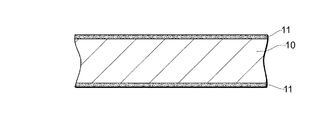
まず、セラミック基板の素地材料を調製し、グリーンシート10を形成する(図1)。具体的には、最初に、非ガラス系材料の素地材料を調製するために、例えば主成分としてバリウム(Ba)、ネオジム(Nd)等の希土類、及びチタン(Ti)の各酸化物を用意し、それらが所定の組成比となるように所定量を秤量し、例えば水等を用いた湿式混合等により混合する。それから、BaO−Nd2O3等の希土類酸化物−TiO2系化合物の合成を行うため、その混合物を、例えば1100℃以上、好ましくは1100℃〜1400℃程度で所定時間、仮焼を行った後、所定の粒径となるように粉砕する。なお、主成分原料としては、酸化物である必要はなく、バリウム、希土類元素、及びチタンの例えば炭酸塩、水酸化物、硫化物等のように熱処理により酸化物となるものを使用してもよい。 First, a base material for a ceramic substrate is prepared to form a green sheet 10 (FIG. 1). Specifically, first, in order to prepare a base material of a non-glass material, for example, rare earth elements such as barium (Ba) and neodymium (Nd) as main components and titanium (Ti) oxides are prepared. A predetermined amount is weighed so that they have a predetermined composition ratio, and mixed by, for example, wet mixing using water or the like. Then, in order to synthesize rare earth oxide-TiO 2 compounds such as BaO—Nd 2 O 3 , the mixture was calcined at a temperature of, for example, 1100 ° C. or higher, preferably about 1100 ° C. to 1400 ° C. for a predetermined time. Then, it grind | pulverizes so that it may become a predetermined particle size. The main component material does not need to be an oxide, and barium, rare earth elements, and titanium such as carbonates, hydroxides, sulfides, and the like that can be converted into oxides by heat treatment may be used. Good.
次に、焼結助剤成分である銅(Cu)、亜鉛(Zn)、及びホウ素(B)の各酸化物の所定量を秤量し、先に仮焼して得た主成分(母材粉末)であるBaO−希土類酸化物−TiO2化合物と、例えば水等を用いた湿式混合等により混合する。このときの主成分と焼結助剤との混合比は特に制限されず、例えば、主成分粉末に対して焼結助剤が0.1〜10質量%程度となるように適宜調整できる。なお、焼結助剤に関しても、主成分原料と同様に、酸化物である必要はなく、例えば、炭酸塩、水酸化物、硫化物等のように熱処理により酸化物となるものを使用してもよい。 Next, a main component (base material powder) obtained by weighing a predetermined amount of each of the oxides of copper (Cu), zinc (Zn), and boron (B), which are sintering aid components, and calcining first. And the BaO-rare earth oxide-TiO 2 compound, for example, by wet mixing using water or the like. The mixing ratio of the main component and the sintering aid at this time is not particularly limited, and can be appropriately adjusted, for example, so that the sintering aid is about 0.1 to 10% by mass with respect to the main component powder. Note that the sintering aid need not be an oxide as in the case of the main component material. For example, a sintering aid that becomes an oxide by heat treatment, such as carbonate, hydroxide, sulfide, etc., is used. Also good.
次いで、主成分と焼結助剤成分との均一分散性を高め、かつ、後工程での成型等の作業性を向上させるべく粒度分布の狭い粉体を得るために、上記の混合粉砕物を、その焼結温度以下の温度で所定時間で再仮焼した後、その仮焼粉末を所定の粒径まで粉砕する。 Next, in order to obtain a powder having a narrow particle size distribution in order to improve the uniform dispersibility of the main component and the sintering aid component and to improve the workability such as molding in a subsequent process, The calcined powder is pulverized to a predetermined particle size after being re-calcined at a temperature equal to or lower than the sintering temperature for a predetermined time.
それから、得られた粉末に、例えば、アクリル系(アクリル酸、メタクリル酸又はそれらのエステルの単独重合体または共重合体、より具体的には、アクリル酸エステル共重合体、メタクリル酸エステル共重合体、アクリル酸エステル−メタクリル酸エステル共重合体等)、ポリビニルブチラール系、ポリビニルアルコール系、アクリル−スチレン系、ポリプロピレンカーボネート系、セルロール系、エチルセルロース系等の単独重合体又は共重合体を適宜の溶剤で溶解したビヒクル等の有機バインダー、或いは、無機バインダー、必要に応じてエステル等の可塑剤やターピネオール等の有機溶剤を混合してスラリーを得る。次に、このスラリーを、例えばドクターブレード法、スラリーキャスト法、スクリーン印刷法、圧延法、プレス法等の適宜の方法によってシート化し、この誘電体のスラリーシートを所望により複数層積層してグリーンシート10を得る。 Then, the obtained powder is made into, for example, acrylic (acrylic acid, methacrylic acid or a homopolymer or copolymer thereof, more specifically, an acrylic ester copolymer, a methacrylic ester copolymer. , Acrylic acid ester-methacrylic acid ester copolymer, etc.), polyvinyl butyral, polyvinyl alcohol, acrylic-styrene, polypropylene carbonate, cellulose, ethyl cellulose, and other homopolymers or copolymers with an appropriate solvent. A dissolved organic binder such as a vehicle, or an inorganic binder, and a plasticizer such as ester and an organic solvent such as terpineol as necessary are mixed to obtain a slurry. Next, the slurry is formed into a sheet by an appropriate method such as a doctor blade method, a slurry casting method, a screen printing method, a rolling method, a pressing method, etc., and a plurality of the slurry sheets of this dielectric are laminated as desired to obtain a green sheet. Get 10.
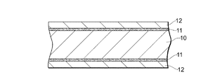
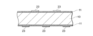
次に、金属ペーストを調製し、この金属ペーストを、グリーンシート10の両面に、例えばスクリーン印刷法、ドクターブレード法、スラリーキャスト法、圧延法、プレス法等によりシート状に塗布し、乾燥させて金属ペースト層(第1の層)を形成する(図2)。この金属ペーストとしては、銀(Ag)、銅(Cu)、銀−パラジウム(Ag−Pd)、金(Au)、白金(Pt)等の粉末(例えば平均粒径が数μmオーダーのもの)に、ポリビニルアルコール系、アクリル系、エチルセルロース系のような有機バインダーを加え、塗布に適した粘度となるように適宜混合したものを用いることができる。また、金属ペーストに含まれる金属についても、当初から金属である必要はなく、例えば、硝酸塩、酸化物、塩化物等のように熱処理により金属となるものを使用することができる。
Next, a metal paste is prepared, and this metal paste is applied to both sides of the
さらに、金属ペーストには適宜の焼結助剤を添加することが好ましい。この焼結助剤としては、非晶質のSiO2、B2O3、Al2O3、ZnO、PbO、Bi2O3、ZrO2、TiO2、アルカリ金属酸化物、アルカリ土類金属酸化物、希土類酸化物等のガラス粉末や、結晶性のSiO2、Al2O3、ZrO2、TiO2、ZnO、MgO、MnO2、MgAl2O4、ZnAl2O4、MgSiO3、Mg2SiO4、Zn2SiO4、Zn2TiO4、SrTiO3、CaTiO3、MgTiO3、BaTiO3、CaMgSi2O6、SrAl2Si2O8、BaAl2Si2O8、CaAl2Si2O8、Mg2Al4Si5O18、Zn2Al4Si5O18、AlN、Si3N4、SiC等のセラミック粉末を、単独で又は複数組み合わせ、適宜選択して用いることができる。
Furthermore, it is preferable to add an appropriate sintering aid to the metal paste. As the sintering aid, amorphous SiO 2 , B 2 O 3 , Al 2 O 3 , ZnO, PbO, Bi 2 O 3 , ZrO 2 , TiO 2 , alkali metal oxide, alkaline earth metal oxidation , Glass powders such as rare earth oxides, crystalline SiO 2 , Al 2 O 3 , ZrO 2 , TiO 2 , ZnO, MgO, MnO 2 , MgAl 2 O 4 , ZnAl 2 O 4 , MgSiO 3 , Mg 2 SiO 4, Zn 2 SiO 4, Zn 2
このとき、金属ペーストに含まれる焼結助剤の化合物又は組成物は、素地材料のグリーンシート10に含まれる焼結助剤と同じ種類のものであると一層好適である。
At this time, the compound or composition of the sintering aid contained in the metal paste is more preferably the same type as the sintering aid contained in the
また、金属ペースト中の金属成分と焼結助剤成分との混合割合は、後述する如く金属ペースト層11の焼成によって形成される配線層導体に要求される電気的性質や機能に応じて適宜設定することができ、例えば、配線層の抵抗やデバイスによっては寄生容量をより小さくするためには、通常、金属100質量部に対して焼結助剤を10質量部程度以下の割合で用いることを例示できる。なお、金属ペーストに用いる金属粉末の性状や形状(例えば、粒状である場合と鱗片状である場合等)によっても、配線層として導通を確保できる金属成分の含有割合は影響を受けるものと想定されるので、金属ペースト中の金属成分と焼結助剤成分との混合割合は、種々の要因に応じて適宜調整され得る。
Further, the mixing ratio of the metal component and the sintering aid component in the metal paste is appropriately set according to the electrical properties and functions required for the wiring layer conductor formed by firing the
次いで、グリーンシート10の焼成温度(グリーンシート10の母剤粉末の焼結温度)では焼結しない難焼結性のセラミック材料粉末に、グリーンシート10用のペースト調製と同様にして有機バインダーを添加、混合してスラリーを調製し、このスラリーを、金属ペースト層11上に、例えば、ドクターブレード法、スラリーキャスト法、スクリーン印刷法、圧延法、プレス法等によりシート状に塗布し、拘束層12(第2の層)を形成し、この状態のものを、例えば熱圧着して図3に示す積層体を得る。
Next, an organic binder is added to the hardly sinterable ceramic material powder that does not sinter at the firing temperature of the green sheet 10 (sintering temperature of the base material powder of the green sheet 10) in the same manner as the paste preparation for the
この拘束層12を形成する難焼結性のセラミック材料としては、例えば、ジルコニア、アルミナ、トリジマイト、トリジマイト、α石英、トリジマイト−α石英、クリストバライト、β石英等が挙げられる。また、焼成時に、拘束層12によるグリーンシート10及び金属ペースト層11の拘束力を高めつつ、有機バインダーを効率よく確実に除去(脱バイ処理)するために、難焼結性のセラミック材料粉末に、グリーンシート10の焼結温度以下でありかつグリーンシート10に含まれる有機成分の分解温度よりも高い軟化点を有するガラス粉末を所定量加えてもよい。
Examples of the hardly sinterable ceramic material for forming the constraining
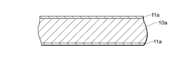
次に、図3に示す積層体を、例えばアルミナセッター等の支持具に載置し、適宜の温度にて脱バイ処理を行った後、例えば850℃〜1050℃程度で所定時間焼成する。このとき、積層体の厚さ方向の焼結収縮を補助・促進するため、積層体上にセラミック板を載せる等の適宜の方法を用いて厚さ方向に加圧するようにしてもよい。そして、焼成後、積層体の両面に未焼結体として残存する拘束層12を、例えば、サンドブラスト、ビーズブラスト、ドライアイスブラスト等の乾式ブラスト処理、水ジェット等やアイスブラスト、スラリーブラスといった湿式ブラスト処理のほか、デスミア処理、プラズマ(アッシング)処理、ジェットスクラブ処理、超音波処理、レーザー処理といった適宜の方法を用いて除去し、グリーンシート10の焼結により形成された誘電体層10a、及び、金属ペースト層11の焼成処理により形成された導体層11aからなる図4に示す焼結積層体を得る。
Next, after placing the laminated body shown in FIG. 3 on a support such as an alumina setter and performing a de-bye treatment at an appropriate temperature, it is fired at a temperature of, for example, about 850 ° C. to 1050 ° C. for a predetermined time. At this time, in order to assist / promote sintering shrinkage in the thickness direction of the laminated body, pressurization in the thickness direction may be performed using an appropriate method such as placing a ceramic plate on the laminated body. Then, after firing, the constraining
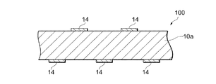
それから、金属ペーストの焼結助剤として用い得る上述したセラミック粉末と、前記の有機バインダーを適宜の割合で混合したセラミック材料ペーストを調製し、このペーストを、導体層11a上にスクリーン印刷等を用いて所望のパターンに塗布し、これを乾燥させることにより、所定のパターンを有するマスク13を形成する(図5)。さらに、このマスク13が積層された部分以外の導体層11aを除去し、誘電体層10a上のマスク13の下部に配線層14を形成する(図6)。このマスク13の積層部分以外の導体層11aを除去する方法としては、図5に示す積層体を、導体層11aの構成金属を溶解する薬液(例えば、導体層11aの金属成分がAgの場合、アンモニア水と過酸化水素水の混合溶液等)に浸漬したり、その積層体上に薬液を流通させたりする湿式化学処理、金属成分を選択的に除去できる条件でのイオンミリングやアッシングといった物理処理を例示できる。
Then, a ceramic material paste is prepared by mixing the above-mentioned ceramic powder that can be used as a sintering aid for the metal paste and the organic binder in an appropriate ratio, and this paste is used on the
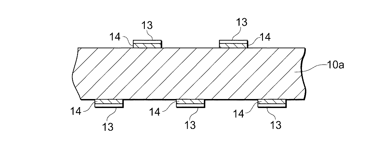
そして、マスク13を上述したブラスト処理等によって除去し、誘電体層10a上に所定のパターンを有する配線層14が形成されたセラミック基板100を得る(図7)。
Then, the
このような本発明によるセラミック基板の製造方法の第1実施形態によれば、セラミック基板の素地材料からなるグリーンシート10上に、金属ペースト層11を介して、難焼結性の拘束層12を積層するので、グリーンシート10中に液相化し得るBa2O3、ZnO、CuO等の焼結助剤が含まれており、その液相化した粘性の低い焼結助剤が拘束層12側へ流動・拡散しようとしても、焼成時に金属ペースト層11から形成される導体層11a(形成途中の状態も含む)が、その液相化焼結助剤の移動を妨げるバリア層として機能する。その結果、液相化した焼結助剤が拘束層12側へ拡散することを抑止することができるので、グリーンシート10の焼結が阻害されることなく、十分な焼結密度ひいては抗折強度を有する誘電体層10aを形成させることができる。よって、セラミック基板材料として、非ガラス系材料を用いても、無収縮プロセスを利用することができるので、製作精度が格段に高められて更なる小型化及び高密度化を実現でき、しかも、実用性に優れた高性能の電子デバイスを得ることができるセラミック基板100を実現できる。
According to the first embodiment of the method for manufacturing a ceramic substrate according to the present invention, the hard-to-
また、金属ペースト層11が焼結助剤を含む場合には、図3に示すグリーンシート10、金属ペースト層11、及び拘束層12の積層体を焼結するときに、金属ペースト層11の焼結性をより高めることができるので、グリーンシート10に含まれる液相化した焼結助剤に対するバリア性を更に向上されることが可能となる。また、金属ペースト層11に含まれる焼結助剤とグリーンシート10に含まれる焼結助剤双方の溶融による相互作用によってグリーンシート10と金属ペースト層11の融着が促進されるとともに、金属ペースト層11とグリーンシート10のそれぞれの焼結挙動を互いに合致させ易くなるので、焼結によって形成される誘電体層10aと導体層11aとの固着強度を格段に高めることができる。
When the
またさらに、金属ペースト層11の構成金属としてCuを用いると、例えばAg等の金属を用いたときに湿分の影響によって生じ得るような金属原子のマイグレーションを防止することができる利点がある。
Further, when Cu is used as the constituent metal of the
また、グリーンシート10に含まれる液相化し得る焼結助剤の拡散防止層として機能する金属ペースト層11から形成される導体層11aを用いて、所望のパターンを有する配線層14を形成するので、金属ペースト層11を有効に利用するして経済性を向上させることができる。さらに、金属ペースト層11から形成される導体層11aを一旦除去してから新たに配線層を形成する手間が省けるので、生産性を高めることもできる。
In addition, the
(第2実施形態)
図8乃至図12は、本発明によるセラミック基板の製造方法の好適な第2実施形態によってセラミック基板を製造する手順を示す工程図(フロー図)であり、各工程におけるセラミック基板の要部を示す概略断面図である。
(Second Embodiment)
FIG. 8 to FIG. 12 are process diagrams (flow diagrams) showing a procedure for manufacturing a ceramic substrate according to a second preferred embodiment of the method for manufacturing a ceramic substrate according to the present invention, and show the main part of the ceramic substrate in each process. It is a schematic sectional drawing.
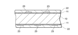
本実施形態においては、まず、第1実施形態と同様にして、グリーンシート10の両面に金属ペースト層11が形成された図2に示す積層体を得る。次に、第1実施形態におけるマスク13の形成と同様にして、金属ペースト層11上に、所定のパターンを有するマスク23を形成する(図8)。さらに、第1実施形態における拘束層12の形成と同様にして、マスク23が設けられた金属ペースト層11上に、拘束層22を形成する(図9)。
In the present embodiment, first, as in the first embodiment, the laminate shown in FIG. 2 in which the metal paste layers 11 are formed on both surfaces of the
次に、この図9に示す積層体を、図3に示す積層体の焼成処理と同様にして焼成した後、積層体の両面に未焼結体として残存する拘束層22を、拘束層12の除去と同様にして除去し、グリーンシート10が焼結して形成された誘電体層10a、金属ペースト層11の焼成処理により形成された導体層11a、その上に所定のパターンを有して形成された焼結マスク23aからなる図10に示す焼結積層体を得る。
Next, after firing the laminate shown in FIG. 9 in the same manner as the firing treatment of the laminate shown in FIG. 3, the constraining
それから、上述したマスク13が積層された部分以外の導体層11aの除去と同様にして、この焼結マスク23aが積層された部分以外の導体層11aを除去し、誘電体層10a上の焼結マスク23aの下部に配線層24を形成する(図11)。
Then, in the same manner as the removal of the
そして、焼結マスク23aを上述したブラスト処理等によって除去し、誘電体層10a上に所定のパターンを有する配線層24が形成されたセラミック基板200を得る(図12)。
Then, the
このような本発明によるセラミック基板の製造方法の第2実施形態によれば、前述した本発明による第1実施形態と同様の作用効果を奏することができる(重複を避けるため、ここでの説明は省略する)。加えて、焼成時に、マスク23のパターンも素地のグリーンシート10と同じ縮率で収縮するので、グリーンシート10に内部電極やビアホール導体等が予め設けられていても、これらと配線層24との位置ずれを防止でき、両者が確実に接続される。その結果、ビアホール導体等が形成されたグリーンシート10から形成される誘電体層10a上に後から配線層を形成する場合のような両者の接続位置のずれを考慮して設計上の寸法裕度を大きくするといった対策が不要となるので、配線構造の微細化による更なる高密度実装が可能となる。
According to the second embodiment of the method for manufacturing a ceramic substrate according to the present invention, the same operational effects as those of the first embodiment according to the present invention described above can be obtained. (Omitted). In addition, since the pattern of the
(第3実施形態)
図13乃至図16は、本発明によるセラミック基板の製造方法の好適な第3実施形態によってセラミック基板を製造する手順を示す工程図(フロー図)であり、各工程におけるセラミック基板の要部を示す概略断面図である。
(Third embodiment)
FIGS. 13 to 16 are process diagrams (flow charts) showing a procedure for manufacturing a ceramic substrate according to a third preferred embodiment of the method for manufacturing a ceramic substrate according to the present invention, and show the main part of the ceramic substrate in each process. It is a schematic sectional drawing.
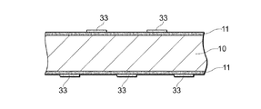
本実施形態においても、まず、第1実施形態と同様にして、グリーンシート10の両面に金属ペースト層11が形成された図2に示す積層体を得る。次に、第1実施形態におけるマスク13の形成と同様にして、金属ペースト層11上に、所定のパターンを有するマスク33を形成する(図13)。このマスク33は、金属ペースト層11と同じ材料からなる組成物からなる。さらに、第1実施形態における拘束層12の形成と同様にして、マスク33が設けられた金属ペースト層11上に、拘束層32を形成する(図14)。
Also in the present embodiment, first, similarly to the first embodiment, the laminate shown in FIG. 2 in which the metal paste layers 11 are formed on both surfaces of the
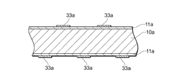
次いで、この図14に示す積層体を、図3に示す積層体の焼成処理と同様にして焼成した後、積層体の両面に未焼結体として残存する拘束層32を、拘束層12の除去と同様にして除去し、グリーンシート10が焼結して形成された誘電体層10a、金属ペースト層11の焼成処理により形成された導体層11a、その上に所定のパターンを有して形成された導体層11aと同組成の金属マスク33aからなる図15に示す焼結積層体を得る。
Next, after firing the laminate shown in FIG. 14 in the same manner as the firing treatment of the laminate shown in FIG. 3, the
その後、上述したマスク13が積層された部分以外の導体層11aの除去と同様のプロセスを図15に示す焼結積層体に適用する。こうすると、導体層11aと金属マスク33aが同組成を有するので、金属マスク33aが積層された部分以外の導体層11aと金属マスク33aとが、同じレートで除去され、金属マスク33aが積層された部分以外の導体層11aが誘電体層10a上に露呈し、所定のパターンを有する配線層34が形成される(図16)。
Thereafter, the same process as the removal of the
このような本発明によるセラミック基板の製造方法の第3実施形態によれば、前述した本発明による第1実施形態及び第2実施形態と同様の作用効果を奏することができる(重複を避けるため、ここでの説明は省略する)。しかも、金属マスク33aが導体層11aと同時に除去されるので、配線層を形成した後にマスクを除去する工程を省略することができ、これにより、生産性を更に一層向上させることができる。
According to the third embodiment of the method for manufacturing a ceramic substrate according to the present invention, the same operational effects as those of the first embodiment and the second embodiment of the present invention described above can be obtained (in order to avoid duplication, The explanation here is omitted). Moreover, since the
なお、上述したとおり、本発明は、上記各実施形態に限定されるものではなく、その要旨を逸脱しない範囲内において適宜変更を加えることが可能である。例えば、非ガラス系材料としては、BaO−Nd2O3等の希土類酸化物−TiO2系化合物以外にも、BaO−Nd2O3等の希土類酸化物−TiO2/MgO−SiO2系化合物、MgO−SiO2系化合物等が挙げられる。また、本発明で用いる素地のグリーンシート10に含まれる母剤のLTCC材料としては、「非ガラス系材料」に制限されず、従来から用いられている「ガラス複合系材料(ガラスコンポジット系材料)」や、例えばSiO2−Al2O3−CaO−BaO−MgOガラス粉末とアルミナ粉末が適宜の割合で混合された「結晶化ガラス系材料」を用いてもよい。
In addition, as above-mentioned, this invention is not limited to said each embodiment, In the range which does not deviate from the summary, it can add suitably. For example, non-glass-based material, BaO-Nd 2 O 3 in addition to rare earth oxide -TiO 2 based compounds such as, rare earth oxides such as BaO-Nd 2 O 3 -TiO 2 / MgO-SiO 2 compound MgO—SiO 2 compounds and the like. Further, the base material LTCC material contained in the
さらに、グリーンシート10の片面側にのみ、金属ペースト層11と拘束層12,22,32を設けて焼成を行ってもよい。またさらに、第1の層である金属ペースト層11は、図17Aに示すように素地のグリーンシート10の全面に一様に形成してもよく、或いは、図17Bに示すように、少なくともグリーンシート10における配線や素子デバイスが形成される領域Rを覆うように形成されていれば、グリーンシート10の全面を覆うように設けなくても構わない。
Furthermore, the
また、金属粉末を含む金属ペースト層11に代えて、金属フィルム又は金属フォイルをグリーンシート10上に貼付又は被着させてもよい。この場合、適宜の方法で金属フィルムや金属フォイルを適宜の基材シート上に形成した後、その金属フィルムや金属フォイルを、基材シートからグリーンシート10上へ転着又は転写することができる。金属ペーストをグリーンシート10上へ塗布するとき、場合によっては、シートの周縁部において厚さが不均一となるおそれがあるのに対し、金属フィルムや金属フォイルは、厚さの均一性を十分に確保し易いので、焼結後の導体層の表面平坦性を向上させ得る利点がある。なお、金属フィルムや金属フォイルを用いる場合、その上に、適宜の焼結助剤を塗布してもよい。
Further, instead of the
以下、本発明の実施例について説明するが、本発明はこれら実施例に限定されるものではない。 Examples of the present invention will be described below, but the present invention is not limited to these examples.
(セラミック基板の素地材料)
表1に示す組成系のLTCC材料、及び、液相形成用の焼結助剤を含有するセラミック基板の素地材料(グリーンシート母剤)を調製した。
(Ceramic substrate material)
The base material (green sheet base material) of the ceramic substrate containing the LTCC material of the composition system shown in Table 1 and the sintering aid for liquid phase formation was prepared.
(実施例1〜4)
上記A材、B材、C材、及びD材をセラミック基板の素地材料として用い、上述した第1実施形態と同様の方法を用いて図4に示す状態のセラミック基板(実施例1〜4)を得た。
(Examples 1-4)
Using the A material, B material, C material, and D material as the base material of the ceramic substrate, the ceramic substrate in the state shown in FIG. 4 using the same method as in the first embodiment described above (Examples 1 to 4) Got.
具体的な条件としては、まず、グリーンシート10として、各素地材料を用いたシート8枚を積層したもの(厚さ約100μm)を形成した。次に、そのグリーンシート10の両面上に、金属としてAg粉末、焼結助剤としてZnO−SiO2系粉末、及び有機バインダーとしてエチルセルロースを含む金属ペーストをスクリーン印刷し、金属ペースト層11(乾燥後の厚さ約15μm)を形成した。さらに、その上に、難焼結性材料としてジルコニア、及び、有機バインダーとしてアクリル系樹脂を含む拘束層12(厚さ約100μm)を形成した。こうして得た図3に示すものと同様の構造を有する積層体を、熱圧着した後、約900℃で所定時間焼成し、さらに、未焼結体として残存した拘束層12をブラスト処理によって除去して図4に示すものと同様の構造を有する焼結積層体を形成した。
As specific conditions, first, a
(参考例1〜4)
評価用の参考例1〜4として、実施例1〜4で形成したグリーンシート10に金属ペースト層及び拘束層を設けることなく、そのままの状態で、約900℃で所定時間焼成し、誘電体層のみからなる焼結体を得た。この焼結体は、無収縮プロセスではなく自由収縮プロセスを適用したものであり、セラミック基板の各素地材料の焼結体に対して望まれる焼結密度及び抗折強度の指標となるものである。
(Reference Examples 1-4)
As reference examples 1 to 4 for evaluation, the
(比較例1)
金属ペースト層11を形成しなかったこと以外は、実施例4(D材)と同様にして焼結体を得た。すなわち、比較例1の焼結体は、グリーンシート10の両面に金属ペースト層11を形成することなく、拘束層12を直接形成して焼結した後、未焼結体として残存する拘束層12をブラスト処理で除去したものである。
(Comparative Example 1)
A sintered body was obtained in the same manner as in Example 4 (D material) except that the
(評価)
実施例1〜4で得たセラミック基板を、アンモニア水と過酸化水素水を同量(50vol%/50vol%)混合した溶液に浸漬し、金属ペースト層11の焼成によって形成された導体層11aを除去した。実施例1〜4から得られたこれらの誘電体層10aのみの焼結体、参考例1〜4で得られた誘電体層10aのみの焼結体、及び、比較例1で得られた誘電体層10aのみの焼結体について、それらの焼結密度及び抗折強度を測定した。なお、焼結密度は、水を用いたアルキメデス法による焼結体の嵩密度と重量の測定結果から算出し、抗折強度の測定は、JIS SR 1601に規定する抗折強度の測定に準拠して行った。得られた結果を表2にまとめて示す。
(Evaluation)
The ceramic substrate obtained in Examples 1 to 4 was immersed in a solution in which ammonia water and hydrogen peroxide water were mixed in the same amount (50 vol% / 50 vol%), and the
これらの結果より、実施例1〜4のセラミック基板の焼結体は、同じ素地材料を用いて自由収縮プロセスで形成された焼結体と同等の焼結密度及び抗折強度を有することが確認された。これに対し、比較例1の焼結体は、同じ素地材料を用いて形成された実施例4のセラミック基板の焼結体及び自由収縮プロセスで形成された参考例4の焼結体に比して、焼結密度及び抗折強度が優位に劣ることが確認された。 From these results, it is confirmed that the sintered bodies of the ceramic substrates of Examples 1 to 4 have the same sintered density and bending strength as the sintered bodies formed by the free shrink process using the same base material. It was done. On the other hand, the sintered body of Comparative Example 1 is compared with the sintered body of the ceramic substrate of Example 4 formed using the same base material and the sintered body of Reference Example 4 formed by the free shrinkage process. Thus, it was confirmed that the sintered density and the bending strength were inferior.
本発明によるセラミック基板の製造方法によれば、セラミック基板の素地材料からなるグリーンシート上に、金属を含む第1の層を介して、難焼結性の拘束層である第2の層を積層形成することにより、素地のグリーンシート中の焼結助剤が液相化しても、その液相化した焼結助剤が第2の層側へ拡散することを防止することができ、これにより、素地に用いるLTCC材料の種類を問わず、無収縮プロセスを利用することができるので、製作精度が格段に高められて更なる小型化及び高密度化を実現でき、かつ、実用性に優れた高性能の電子デバイスを得ることができる。以上のことから、本発明によるセラミック基板の製造方法は、LTCC材料を用いた電子デバイス、及び、それらを備える機器、装置、システム、設備等、並びに、それらの製造に、広くかつ有効に利用することができる。 According to the method for manufacturing a ceramic substrate according to the present invention, the second layer which is a hard-to-sinter constraining layer is laminated on the green sheet made of the base material of the ceramic substrate via the first layer containing metal. By forming, even if the sintering aid in the green sheet of the substrate becomes a liquid phase, it is possible to prevent the liquid phase sintering aid from diffusing to the second layer side. Regardless of the type of LTCC material used for the substrate, a non-shrinking process can be used, so that the manufacturing accuracy can be remarkably increased, further miniaturization and higher density can be realized, and excellent practicality A high-performance electronic device can be obtained. From the above, the method for manufacturing a ceramic substrate according to the present invention is widely and effectively used for electronic devices using LTCC materials, and devices, apparatuses, systems, facilities, and the like including them, and their manufacture. be able to.
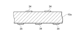
10…グリーンシート、10a…誘電体層、11…金属ペースト層(第1の層)、11a…導体層、12,22,32…拘束層(第2の層)、13,23,33…マスク、14,24,34…配線層、23…焼結マスク、23a…焼結マスク、33a…金属マスク、100,200…セラミック基板、R…領域。
DESCRIPTION OF
Claims (5)
前記グリーンシートの少なくとも片面に金属を含む第1の層を形成し、
前記第1の層上に、前記第1の層上に所定のマスクパターンを形成した後、さらに前記素地材料の焼成温度では焼結しない第2の層を形成し、
前記第2の層が形成された積層体を焼成し、
前記焼成された積層体から前記第2の層を除去し、
前記第2の層が除去された後の前記第1の層を、前記マスクパターンを用いてパターニングすることにより配線層を形成する、
セラミック基板の製造方法。 Form a green sheet made of ceramic substrate material,
Forming a first layer containing metal on at least one side of the green sheet;
On the first layer, after forming a predetermined mask pattern on the first layer, further forming a second layer that does not sinter at the firing temperature of the base material,
Firing the laminate on which the second layer is formed;
The calcined said second layer is removed from the stack,
Forming a wiring layer by patterning the first layer after the second layer is removed using the mask pattern ;
A method for manufacturing a ceramic substrate.
請求項1記載のセラミック基板の製造方法。 A non-glass material is used as the base material.
The method for producing a ceramic substrate according to claim 1.
請求項1又は2記載のセラミック基板の製造方法。 The first layer includes a sintering aid;
A method for producing a ceramic substrate according to claim 1 or 2.
前記マスクを用いて前記第1の層をパターニングすることにより前記配線層を形成する、
請求項1記載のセラミック基板の製造方法。 Forming a mask having a predetermined pattern on the first layer from which the second layer has been removed;
Forming the wiring layer by patterning the first layer using the mask;
The method for producing a ceramic substrate according to claim 1 .
前記第2の層が除去された後の前記第1の層を、前記マスクパターンを用いてパターニングすることにより前記配線層を形成する、 Forming the wiring layer by patterning the first layer after the second layer is removed using the mask pattern;
請求項1記載のセラミック基板の製造方法。The method for producing a ceramic substrate according to claim 1.
Priority Applications (1)
| Application Number | Priority Date | Filing Date | Title |
|---|---|---|---|
| JP2008046729A JP4831492B2 (en) | 2008-02-27 | 2008-02-27 | Manufacturing method of ceramic substrate |
Applications Claiming Priority (1)
| Application Number | Priority Date | Filing Date | Title |
|---|---|---|---|
| JP2008046729A JP4831492B2 (en) | 2008-02-27 | 2008-02-27 | Manufacturing method of ceramic substrate |
Publications (2)
| Publication Number | Publication Date |
|---|---|
| JP2009206282A JP2009206282A (en) | 2009-09-10 |
| JP4831492B2 true JP4831492B2 (en) | 2011-12-07 |
Family
ID=41148264
Family Applications (1)
| Application Number | Title | Priority Date | Filing Date |
|---|---|---|---|
| JP2008046729A Expired - Fee Related JP4831492B2 (en) | 2008-02-27 | 2008-02-27 | Manufacturing method of ceramic substrate |
Country Status (1)
| Country | Link |
|---|---|
| JP (1) | JP4831492B2 (en) |
Family Cites Families (6)
| Publication number | Priority date | Publication date | Assignee | Title |
|---|---|---|---|---|
| JPH0590734A (en) * | 1991-09-27 | 1993-04-09 | Nikko Co | Method for forming conductor on ceramic board and method for forming conductor circuit pattern |
| JP3197147B2 (en) * | 1993-10-15 | 2001-08-13 | 松下電器産業株式会社 | Method for manufacturing multilayer ceramic substrate |
| JP3663670B2 (en) * | 1995-05-31 | 2005-06-22 | 株式会社デンソー | Semiconductor wafer splitting device |
| JP2000151067A (en) * | 1998-11-06 | 2000-05-30 | Mitsui Mining & Smelting Co Ltd | Novel printed wiring board and manufacturing multilayer printed wiring board |
| JP3646587B2 (en) * | 1999-10-27 | 2005-05-11 | 株式会社村田製作所 | Multilayer ceramic substrate and manufacturing method thereof |
| JP2006093567A (en) * | 2004-09-27 | 2006-04-06 | Kyocera Corp | Method for manufacturing electronic component |
-
2008
- 2008-02-27 JP JP2008046729A patent/JP4831492B2/en not_active Expired - Fee Related
Also Published As
| Publication number | Publication date |
|---|---|
| JP2009206282A (en) | 2009-09-10 |
Similar Documents
| Publication | Publication Date | Title |
|---|---|---|
| JP4557417B2 (en) | Manufacturing method of low-temperature fired ceramic wiring board | |
| JP3897472B2 (en) | Passive component built-in multilayer wiring board and manufacturing method thereof | |
| JP3652196B2 (en) | Manufacturing method of ceramic wiring board | |
| US20200135400A1 (en) | Multilayer ceramic electronic component and method of manufacturing the same | |
| JP3955389B2 (en) | Capacitor-embedded substrate and manufacturing method thereof | |
| JP2010080866A (en) | Multilayer wiring board and method for manufacturing the same | |
| JP4831492B2 (en) | Manufacturing method of ceramic substrate | |
| JP2002290043A (en) | Manufacturing method of ceramic wiring circuit board | |
| JP4578134B2 (en) | Glass ceramic multilayer wiring board with built-in capacitor | |
| JP4688460B2 (en) | Glass ceramic multilayer wiring board with built-in capacitor | |
| JP2004228410A (en) | Wiring board | |
| JP4496529B2 (en) | Multilayer ceramic substrate manufacturing method and multilayer ceramic substrate | |
| JP2010153554A (en) | Ceramic substrate, and method of manufacturing the same | |
| JP4817855B2 (en) | Capacitor built-in wiring board and manufacturing method thereof | |
| JP2006179844A (en) | Wiring board with built-in capacitor | |
| JP2007201276A (en) | Wiring board | |
| JP5110419B2 (en) | Ag powder, conductor paste, multilayer ceramic substrate and manufacturing method thereof | |
| JP4658465B2 (en) | Glass ceramic multilayer wiring board with built-in capacitor | |
| JPH11157945A (en) | Production of ceramic electronic part and green sheet for dummy used therefor | |
| JP2002353626A (en) | Multilayer wiring board and method of manufacturing the same | |
| JP4530864B2 (en) | Wiring board with built-in capacitor | |
| JP2007201272A (en) | Manufacturing method of wiring board | |
| JP2006089352A (en) | Dielectric paste and glass ceramic multilayer wiring board with built-in capacitor | |
| JP2010034270A (en) | Method of manufacturing multilayered wiring board | |
| JP2006278759A (en) | Wiring board |
Legal Events
| Date | Code | Title | Description |
|---|---|---|---|
| A977 | Report on retrieval |
Free format text: JAPANESE INTERMEDIATE CODE: A971007 Effective date: 20110316 |
|
| A131 | Notification of reasons for refusal |
Free format text: JAPANESE INTERMEDIATE CODE: A131 Effective date: 20110325 |
|
| A521 | Written amendment |
Free format text: JAPANESE INTERMEDIATE CODE: A523 Effective date: 20110513 |
|
| TRDD | Decision of grant or rejection written | ||
| A01 | Written decision to grant a patent or to grant a registration (utility model) |
Free format text: JAPANESE INTERMEDIATE CODE: A01 Effective date: 20110826 |
|
| A01 | Written decision to grant a patent or to grant a registration (utility model) |
Free format text: JAPANESE INTERMEDIATE CODE: A01 |
|
| A61 | First payment of annual fees (during grant procedure) |
Free format text: JAPANESE INTERMEDIATE CODE: A61 Effective date: 20110908 |
|
| R150 | Certificate of patent (=grant) or registration of utility model |
Free format text: JAPANESE INTERMEDIATE CODE: R150 |
|
| FPAY | Renewal fee payment (prs date is renewal date of database) |
Free format text: PAYMENT UNTIL: 20140930 Year of fee payment: 3 |
|
| LAPS | Cancellation because of no payment of annual fees |