JP4826213B2 - Level shift circuit, shift register and display device - Google Patents
Level shift circuit, shift register and display device Download PDFInfo
- Publication number
- JP4826213B2 JP4826213B2 JP2005320938A JP2005320938A JP4826213B2 JP 4826213 B2 JP4826213 B2 JP 4826213B2 JP 2005320938 A JP2005320938 A JP 2005320938A JP 2005320938 A JP2005320938 A JP 2005320938A JP 4826213 B2 JP4826213 B2 JP 4826213B2
- Authority
- JP
- Japan
- Prior art keywords
- voltage
- period
- node
- circuit
- signal
- Prior art date
- Legal status (The legal status is an assumption and is not a legal conclusion. Google has not performed a legal analysis and makes no representation as to the accuracy of the status listed.)
- Expired - Fee Related
Links
Images


Classifications
-
- B—PERFORMING OPERATIONS; TRANSPORTING
- B60—VEHICLES IN GENERAL
- B60J—WINDOWS, WINDSCREENS, NON-FIXED ROOFS, DOORS, OR SIMILAR DEVICES FOR VEHICLES; REMOVABLE EXTERNAL PROTECTIVE COVERINGS SPECIALLY ADAPTED FOR VEHICLES
- B60J11/00—Removable external protective coverings specially adapted for vehicles or parts of vehicles, e.g. parking covers
- B60J11/02—Covers wound on rollers
-
- G—PHYSICS
- G11—INFORMATION STORAGE
- G11C—STATIC STORES
- G11C19/00—Digital stores in which the information is moved stepwise, e.g. shift registers
- G11C19/18—Digital stores in which the information is moved stepwise, e.g. shift registers using capacitors as main elements of the stages
- G11C19/182—Digital stores in which the information is moved stepwise, e.g. shift registers using capacitors as main elements of the stages in combination with semiconductor elements, e.g. bipolar transistors, diodes
- G11C19/184—Digital stores in which the information is moved stepwise, e.g. shift registers using capacitors as main elements of the stages in combination with semiconductor elements, e.g. bipolar transistors, diodes with field-effect transistors, e.g. MOS-FET
-
- H—ELECTRICITY
- H03—ELECTRONIC CIRCUITRY
- H03K—PULSE TECHNIQUE
- H03K19/00—Logic circuits, i.e. having at least two inputs acting on one output; Inverting circuits
- H03K19/0175—Coupling arrangements; Interface arrangements
- H03K19/0185—Coupling arrangements; Interface arrangements using field effect transistors only
- H03K19/018507—Interface arrangements
- H03K19/01855—Interface arrangements synchronous, i.e. using clock signals
-
- G—PHYSICS
- G09—EDUCATION; CRYPTOGRAPHY; DISPLAY; ADVERTISING; SEALS
- G09G—ARRANGEMENTS OR CIRCUITS FOR CONTROL OF INDICATING DEVICES USING STATIC MEANS TO PRESENT VARIABLE INFORMATION
- G09G2310/00—Command of the display device
- G09G2310/02—Addressing, scanning or driving the display screen or processing steps related thereto
- G09G2310/0264—Details of driving circuits
- G09G2310/0286—Details of a shift registers arranged for use in a driving circuit
-
- G—PHYSICS
- G09—EDUCATION; CRYPTOGRAPHY; DISPLAY; ADVERTISING; SEALS
- G09G—ARRANGEMENTS OR CIRCUITS FOR CONTROL OF INDICATING DEVICES USING STATIC MEANS TO PRESENT VARIABLE INFORMATION
- G09G2310/00—Command of the display device
- G09G2310/02—Addressing, scanning or driving the display screen or processing steps related thereto
- G09G2310/0264—Details of driving circuits
- G09G2310/0289—Details of voltage level shifters arranged for use in a driving circuit
Landscapes
- Engineering & Computer Science (AREA)
- Computer Hardware Design (AREA)
- Microelectronics & Electronic Packaging (AREA)
- General Engineering & Computer Science (AREA)
- Physics & Mathematics (AREA)
- Computing Systems (AREA)
- Power Engineering (AREA)
- Mathematical Physics (AREA)
- Mechanical Engineering (AREA)
- Control Of Indicators Other Than Cathode Ray Tubes (AREA)
- Logic Circuits (AREA)
- Shift Register Type Memory (AREA)
- Liquid Crystal Display Device Control (AREA)
- Electronic Switches (AREA)
- Control Of El Displays (AREA)
Description
本発明は、入力信号の振幅を変換するレベルシフト回路とこのレベルシフト回路を搭載する表示装置に係り、特に、液晶表示装置や有機EL(OLED)表示装置などの表示装置に用いられるレベルシフト回路に関するものである。 The present invention relates to a level shift circuit for converting the amplitude of an input signal and a display device equipped with the level shift circuit, and in particular, a level shift circuit used for a display device such as a liquid crystal display device or an organic EL (OLED) display device. It is about.
レベルシフト回路には従来から種々の方式があり、例えば、カレントミラー回路を用いて構成されたレベルシフト回路が知られている(例えば、特許文献1参照)。 Conventionally, there are various types of level shift circuits. For example, a level shift circuit configured using a current mirror circuit is known (for example, see Patent Document 1).
図41は、従来のカレントミラー型レベルシフト回路の構成の一例を示す図である。
図41に示すカレントミラー型レベルシフト回路200は、回路動作制御部201と、2つのバイアスシフト部202および203と、レベルシフト部204と、出力部205とを有する。
FIG. 41 is a diagram showing an example of the configuration of a conventional current mirror type level shift circuit.
A current mirror type
回路動作制御部201は、p型MOSトランジスタQp201,Qp202と、n型MOSトランジスタQn201とを有する。
p型MOSトランジスタQp201およびn型MOSトランジスタQn201は、正側の電源電圧VDDが供給される電源ライン(以下、「電源ラインVDD」と表記する)と、負側の電源電圧VSSが供給される電源ライン(以下、「電源ラインVSS」と表記する)との間に直列に接続され、ゲート同士およびドレイン同士がそれぞれ共通に接続されている。
p型MOSトランジスタQp202は、そのソースが電源ラインVDDに接続され、そのゲートがp型MOSトランジスタQp201およびn型MOSトランジスタQn201の各ゲートに接続される。
The circuit
The p-type MOS transistor Qp201 and the n-type MOS transistor Qn201 include a power supply line to which a positive power supply voltage VDD is supplied (hereinafter referred to as “power supply line VDD”) and a power supply to which a negative power supply voltage VSS is supplied. Lines (hereinafter referred to as “power supply line VSS”) are connected in series, and gates and drains are connected in common.
The p-type MOS transistor Qp202 has a source connected to the power supply line VDD and a gate connected to each gate of the p-type MOS transistor Qp201 and the n-type MOS transistor Qn201.
p型MOSトランジスタQp201およびn型MOSトランジスタQn201の共通接続されたゲートには、回路動作制御信号XSTBが入力される。この回路動作制御信号XSTBは、回路のスタンバイ時(非駆動時)においてローレベルに設定され、回路の駆動時においてハイレベルに設定される。 A circuit operation control signal XSTB is input to the commonly connected gates of the p-type MOS transistor Qp201 and the n-type MOS transistor Qn201. The circuit operation control signal XSTB is set to a low level when the circuit is on standby (not driven), and is set to a high level when the circuit is driven.
バイアスシフト部202は、p型MOSトランジスタQp203,Qp204と、n型MOSトランジスタQn202とを有する。
p型MOSトランジスタp203およびn型MOSトランジスタQn202は、電源ラインVDDと電源ラインVSSとの間に直列に接続され、互いのゲートがp型MOSトランジスタQp201およびn型MOSトランジスタQn201のドレインに共通に接続される。p型MOSトランジスタQp204は、n型MOSトランジスタQn202と並列に接続され、そのゲートにクロック信号CKが入力される。
このバイアスシフト部202においては、クロック信号CKの直流バイアスをシフトする動作が行われる。
The
The p-type MOS transistor p203 and the n-type MOS transistor Qn202 are connected in series between the power supply line VDD and the power supply line VSS, and their gates are commonly connected to the drains of the p-type MOS transistor Qp201 and the n-type MOS transistor Qn201. Is done. The p-type MOS transistor Qp204 is connected in parallel with the n-type MOS transistor Qn202, and the clock signal CK is input to its gate.
In the
バイアスシフト部203は、p型MOSトランジスタQp205,Qp206と、n型MOSトランジスタQn203とを有する。
p型MOSトランジスタQp205およびn型MOSトランジスタQn203は、電源ラインVDDと電源ラインVSSとの間に直列に接続され、互いのゲートが共通に接続される。p型MOSトランジスタQp206は、n型MOSトランジスタQn203と並列に接続され、そのゲートにクロック信号xCKが入力される。クロック信号xCKは、クロック信号CKに対して逆相の信号である。
このバイアスシフト部203においては、逆相のクロック信号xCKの直流バイアスをシフトする動作が行われる。
The
The p-type MOS transistor Qp205 and the n-type MOS transistor Qn203 are connected in series between the power supply line VDD and the power supply line VSS, and their gates are connected in common. The p-type MOS transistor Qp206 is connected in parallel with the n-type MOS transistor Qn203, and the clock signal xCK is input to the gate thereof. The clock signal xCK is a signal having a phase opposite to that of the clock signal CK.
In the
レベルシフト部204は、p型MOSトランジスタQp207,p208と、n型MOSトランジスタQn204,Qn205とを有する。
p型MOSトランジスタQp207およびQp208は、カレントミラー回路を構成する。p型MOSトランジスタQp207およびQp208のソースは電源ラインVDDに共通接続され、そのゲートはp型MOSトランジスタQp207のドレインに共通接続される。p型MOSトランジスタQp207のドレインは、p型MOSトランジスタQp202のドレインに接続される。
n型MOSトランジスタQn204は、そのドレインがp型MOSトランジスタQp207のドレインに接続され、そのゲートがp型MOSトランジスタQp203およびn型MOSトランジスタQn202のドレインに接続され、そのソースにクロック信号xCKが入力される。n型MOSトランジスタQn205は、そのドレインがp型MOSトランジスタQp208のドレインに接続され、そのゲートがp型MOSトランジスタQp205およびn型MOSトランジスタQn203のドレインに接続され、そのソースにクロック信号CKが入力される。
このレベルシフト部204は、互いに逆位相のクロック信号xCKおよびCKをn型MOSトランジスタQn204およびn205のソースに入力するカレントミラーアンプを構成する。
The
The p-type MOS transistors Qp207 and Qp208 constitute a current mirror circuit. The sources of p-type MOS transistors Qp207 and Qp208 are commonly connected to power supply line VDD, and their gates are commonly connected to the drain of p-type MOS transistor Qp207. The drain of p-type MOS transistor Qp207 is connected to the drain of p-type MOS transistor Qp202.
N-type MOS transistor Qn204 has its drain connected to the drain of p-type MOS transistor Qp207, its gate connected to the drains of p-type MOS transistor Qp203 and n-type MOS transistor Qn202, and clock signal xCK input to its source. The N-type MOS transistor Qn205 has its drain connected to the drain of p-type MOS transistor Qp208, its gate connected to the drains of p-type MOS transistor Qp205 and n-type MOS transistor Qn203, and a clock signal CK input to its source. The
The
出力部205は、n型MOSトランジスタQ206を有する。n型MOSトランジスタQ206は、そのドレインがp型MOSトランジスタQp208およびn型MOSトランジスタQn205のドレインに接続され、そのソースが電源ラインVSSに接続され、そのゲートがp型MOSトランジスタQp205およびn型MOSトランジスタQn203のゲートに接続される。
図41に示すレベルシフト回路200では、カレントミラー回路を構成する対のp型MOSトランジスタQp207,Qp208の特性が良く揃っている必要があるため、トランジスタの特性のばらつきに回路の動作が影響を受け易い。
In the
また、このレベルシフト回路200では、カレントミラー回路の動作に伴ってトランジスタにリーク電流が流れる。すなわち、クロック信号CK,xCKの直流バイアスをシフトするバイアスシフト部202および203と、このクロック信号CK,xCKの振幅を電源電圧VSS−VDDの振幅に変換するレベルシフト部204とにおいて、図中の点線で示した経路にリーク電流が流れる。そのため、レベルシフト回路200は、リーク電流による消費電力が大きくなる。
In the
本発明はかかる事情に鑑みてなされたものであり、その目的は、トランジスタ等の素子の特性ばらつきに回路動作が影響を受け難いレベルシフト回路およびシフトレジスタと、そのようなレベルシフト回路やシフトレジスタを搭載する表示装置を提供することにある。 The present invention has been made in view of such circumstances, and an object of the present invention is to provide a level shift circuit and a shift register in which circuit operation is hardly affected by variations in characteristics of elements such as transistors, and such a level shift circuit and a shift register. It is to provide a display device equipped with.
本発明の第1の観点に係るレベルシフト回路は、入力信号をレベルシフトして出力する。このレベルシフト回路は、第1のノードの電圧に応じてオンまたはオフし、当該電圧が第1のしきい値のときにオンとオフとを切り換え、当該オンのとき、レベルシフト信号の出力端子へ第1の電圧を出力する第1のスイッチと、第2のノードの電圧に応じてオンまたはオフし、当該電圧が第2のしきい値のときにオンとオフとを切り換え、当該オンのとき、上記出力端子へ第2の電圧を出力する第2のスイッチと、一方の端子に第1の入力信号を入力し、他方の端子が上記第1のノードに接続される第1のキャパシタと、一方の端子に第2の入力信号を入力し、他方の端子が上記第2のノードに接続される第2のキャパシタと、所定の期間において、上記第1のノードを上記第2の電圧で充電した状態から当該第1のノードの電圧を上記第1のしきい値に設定し、上記第2のノードを上記第1の電圧で充電した状態から当該第2のノードの電圧を上記第2のしきい値に設定する電圧設定回路とを有する。 The level shift circuit according to the first aspect of the present invention level-shifts an input signal and outputs it. The level shift circuit is turned on or off according to the voltage of the first node, and is switched on and off when the voltage is the first threshold value. When the voltage is on, the level shift signal output terminal The first switch that outputs the first voltage to the first node and the second switch is turned on or off according to the voltage of the second node, and is switched on and off when the voltage is the second threshold value. A second switch that outputs a second voltage to the output terminal; a first capacitor that inputs a first input signal to one terminal and the other terminal is connected to the first node; The second input signal is input to one terminal, the other terminal is connected to the second node, and the first node is applied with the second voltage in a predetermined period. the first voltage of the first node from the charging state The set threshold, and a said second node of the voltage the second voltage setting Ru set Teisu the threshold of the second node from the state of being charged by the first voltage circuit .
本発明の第2の観点に係るシフトレジスタは、初段に入力されたパルス信号を後段へ順次に伝送する、縦続接続された複数のシフト段を具備する。
上記シフト段は、前段からパルス信号が入力される期間、並びに、次段へパルス信号が出力される期間を検出する検出回路と、上記検出回路が検出したパルス信号の入力期間および出力期間において、入力されるクロック信号の1サイクル内に含まれるパルス信号をレベルシフトして出力するレベルシフト回路と、上記検出回路が検出したパルス信号の入力期間および出力期間において、上記レベルシフト回路から出力される信号をパルス信号として次段に出力し、上記レベルシフト回路を初期化する所定の期間において、一定のレベルの信号を次段に出力する出力回路とを有する。
上記レベルシフト回路は、第1のノードの電圧が、第1の電圧から第2の電圧までの範囲に含まれる第1のしきい値に対して上記第2の電圧側にある場合にオンし、上記第1のノードの電圧が、上記第1のしきい値に対して上記第1の電圧側にある場合にオフし、当該オンのとき、レベルシフト信号の出力端子へ上記第1の電圧を出力する第1のスイッチと、第2のノードの電圧が、上記第1の電圧から上記第2の電圧までの範囲に含まれる第2のしきい値に対して上記第1の電圧側にある場合にオンし、上記第2のノードの電圧が、上記第2のしきい値に対して上記第2の電圧側にある場合にオフし、当該オンのとき、上記出力端子へ上記第2の電圧を出力する第2のスイッチと、一方の端子に上記クロック信号を入力し、他方の端子が上記第1のノードに接続される第1のキャパシタと、一方の端子に上記クロック信号を入力し、他方の端子が上記第2のノードに接続される第2のキャパシタと、上記所定の期間において、上記第1のノードを上記第2の電圧で充電した状態から当該第1のノードの電圧を上記第1のしきい値に設定し、上記第2のノードを上記第1の電圧で充電した状態から当該第2のノードの電圧を上記第2のしきい値に設定する電圧設定回路と、上記検出回路が検出したパルス信号の入力期間および出力期間において、上記クロック信号を上記第1のキャパシタおよび上記第2のキャパシタに入力する第1の入力回路と、上記電圧設定回路が上記第1のノードおよび上記第2のノードの電圧設定を行う期間において、第3の電圧から第4の電圧までの範囲に含まれる所定の電圧を上記クロック信号の代わりに上記第1のキャパシタおよび上記第2のキャパシタに入力する第2の入力回路とを有する。
上記クロック信号は、上記第3の電圧と上記第4の電圧を交互に繰り返す信号であり、縦続接続される2つのシフト段は、互いの周期が等しく位相が異なるクロック信号を入力する。
A shift register according to a second aspect of the present invention includes a plurality of cascade-connected shift stages that sequentially transmit a pulse signal input to the first stage to the subsequent stage.
The shift stage includes a detection circuit that detects a period in which a pulse signal is input from the previous stage, a period in which the pulse signal is output to the next stage, and an input period and an output period of the pulse signal detected by the detection circuit. A level shift circuit for level-shifting and outputting a pulse signal included in one cycle of an input clock signal, and an output period from the level shift circuit in the input period and output period of the pulse signal detected by the detection circuit The output circuit outputs a signal to the next stage as a pulse signal, and outputs a signal of a certain level to the next stage in a predetermined period for initializing the level shift circuit.
The level shift circuit is turned on when the voltage of the first node is on the second voltage side with respect to the first threshold included in the range from the first voltage to the second voltage. When the voltage at the first node is on the first voltage side with respect to the first threshold, the first voltage is applied to the output terminal of the level shift signal when the voltage is on. And a voltage at a second node on the first voltage side with respect to a second threshold included in a range from the first voltage to the second voltage. Turns on in some cases, turns off when the voltage of the second node is on the second voltage side with respect to the second threshold value, and turns on the second terminal to the output terminal when turned on. The second switch that outputs the voltage of the above and the clock signal is input to one terminal and the other terminal is A first capacitor connected to the first node, and receives one of the clock signals to the terminal, a second capacitor and the other terminal connected to the second node, in the predetermined time period, A state in which the voltage of the first node is set to the first threshold value from the state in which the first node is charged with the second voltage, and the second node is charged with the first voltage. from a voltage setting circuit Ru set Teisu the voltage of the second node to the second threshold value, the input period and an output period of the pulse signal the detection circuit detects, said clock signal said first A first input circuit that inputs to the capacitor and the second capacitor; and a period from when the voltage setting circuit sets the voltage of the first node and the second node to the fourth voltage. Range up to A predetermined voltage contained and a second input circuit for inputting to said first capacitor and said second capacitor in place of the clock signal.
The clock signal is a signal that alternately repeats the third voltage and the fourth voltage, and the two shift stages connected in cascade input clock signals having the same period and different phases.
本発明の第3の観点に係る表示装置は、入力信号をレベルシフトして出力するレベルシフト回路と、複数の画素を含む画素アレイ部と、上記レベルシフト回路から出力されるレベルシフト信号に応じて上記画素アレイ部の各画素を駆動する駆動回路とを有する。第3の観点に係る表示装置は、このレベルシフト回路として、上記第1の観点に係るレベルシフト回路を有する。 According to a third aspect of the present invention, there is provided a display device according to a level shift circuit for level-shifting and outputting an input signal, a pixel array unit including a plurality of pixels, and a level shift signal output from the level shift circuit. And a driving circuit for driving each pixel of the pixel array portion. The display device according to the third aspect includes the level shift circuit according to the first aspect as the level shift circuit.
本発明の第4の観点に係る表示装置は、行列状に配列された複数の画素を含む画素アレイ部と駆動回路とを具備する。上記駆動回路は、上記画素アレイ部の各行を順番に選択するパルス信号を発生する第1のシフトレジスタと、当該選択した行に属する各画素を順番に選択するパルス信号を発生する第2のシフトレジスタとを有しており、選択した画素を駆動する。第4の観点に係る表示装置は、この第1のシフトレジスタおよび第2のシフトレジスタとして、上記第2の観点に係るシフトレジスタを有する。 A display device according to a fourth aspect of the present invention includes a pixel array unit including a plurality of pixels arranged in a matrix and a drive circuit. The driving circuit includes a first shift register that generates a pulse signal that sequentially selects each row of the pixel array unit, and a second shift that generates a pulse signal that sequentially selects each pixel belonging to the selected row. And a register to drive the selected pixel. The display device according to the fourth aspect includes the shift register according to the second aspect as the first shift register and the second shift register.
上記本発明によると、上記所定の期間において、上記第1のノードの電圧は上記第1のしきい値に設定され、上記第2のノードの電圧は上記第2のしきい値に設定される。そして、この所定の期間の後、上記第1のノードおよび上記第2のノードは、フローティング状態に設定される。
この状態で、上記第1の入力信号の電圧が僅かに変化すると、上記第1のノードはフローティング状態にあるため、上記第1の入力信号の電圧変化に応じて上記第1のノードの電圧が上記第1のしきい値から変化し、上記第1のスイッチのオンとオフが切り換わる。
また、この状態で、上記第2の入力信号の電圧が僅かに変化すると、上記第2のノードはフローティング状態にあるため、上記第2の入力信号の電圧変化に応じて上記第2のノードの電圧が上記第2のしきい値から変化し、上記第2のスイッチのオンとオフが切り換わる。
例えば、上記第1のスイッチがオフからオン、上記第2のスイッチがオンからオフへ変化するように上記第1の入力信号および上記第2の入力信号の電圧が僅かに変化すると、上記出力端子の電圧は、上記第2の電圧から上記第1の電圧へ変化する。逆に、上記第2のスイッチがオンからオフ、上記第2のスイッチがオフからオンへ変化するように上記第1の入力信号および上記第2の入力信号の電圧が僅かに変化すると、上記出力端子の電圧は、上記第1の電圧から上記第2の電圧へ変化する。
このように、上記第1の入力信号および上記第2の入力信号の僅かな電圧変化によって、上記出力端子からは、上記第1の電圧と上記第2の電圧との間で変化するレベルシフト信号が出力される。
According to the present invention, in the predetermined period, the voltage of the first node is set to the first threshold value, and the voltage of the second node is set to the second threshold value. . Then, after the predetermined period, the first node and the second node are set in a floating state.
In this state, when the voltage of the first input signal slightly changes, the first node is in a floating state, so that the voltage of the first node changes according to the voltage change of the first input signal. The first threshold value is changed, and the first switch is switched on and off.
Further, in this state, if the voltage of the second input signal slightly changes, the second node is in a floating state, and therefore, the second node in response to the voltage change of the second input signal. The voltage changes from the second threshold value, and the second switch is turned on and off.
For example, when the voltages of the first input signal and the second input signal change slightly so that the first switch changes from off to on and the second switch changes from on to off, the output terminal The voltage changes from the second voltage to the first voltage. Conversely, when the voltages of the first input signal and the second input signal change slightly so that the second switch changes from on to off and the second switch changes from off to on, the output The voltage at the terminal changes from the first voltage to the second voltage.
As described above, the level shift signal that changes between the first voltage and the second voltage from the output terminal due to a slight voltage change of the first input signal and the second input signal. Is output.
上記第1のしきい値および上記第2のしきい値は、好適には、上記第1の電圧から上記第2の電圧までの範囲に含まれる。
また、好適には、上記第1のスイッチは、上記第1のノードの電圧が上記第1のしきい値に対して上記第2の電圧側にある場合にオンし、上記第1の電圧側にある場合にオフし、上記第2のスイッチは、上記第2のノードの電圧が上記第2のしきい値に対して上記第1の電圧側にある場合にオンし、上記第2の電圧側にある場合にオフする。
この場合、上記電圧設定回路は、第1の期間において、上記第1のノードの電圧が上記第1のしきい値に対して上記第2の電圧側にあるように上記第1のキャパシタを充電し、当該充電後の第2の期間において、オン状態の上記第1のスイッチから出力される電圧を上記第1のノードに供給し、第3の期間において、上記第2のノードの電圧が上記第2のしきい値に対して上記第1の電圧側にあるように上記第2のキャパシタを充電し、当該充電後の第4の期間において、オン状態の上記第2のスイッチから出力される電圧を上記第2のノードに供給しても良い。
The first threshold value and the second threshold value are preferably included in a range from the first voltage to the second voltage.
Preferably, the first switch is turned on when the voltage of the first node is on the second voltage side with respect to the first threshold value, and the first voltage side is turned on. The second switch is turned on when the voltage of the second node is on the first voltage side with respect to the second threshold value, and the second voltage is turned off. Turn off when on the side.
In this case, the voltage setting circuit charges the first capacitor so that the voltage of the first node is on the second voltage side with respect to the first threshold value in the first period. In the second period after the charging, the voltage output from the first switch in the on state is supplied to the first node, and in the third period, the voltage of the second node is The second capacitor is charged so as to be on the first voltage side with respect to the second threshold value, and is output from the second switch in the on state in the fourth period after the charging. A voltage may be supplied to the second node.
また、上記電圧設定回路は、上記第2の期間において上記第1のスイッチがオフした後、上記第3の期間における上記第2のキャパシタの充電を行っても良い。
この場合、好適には、上記電圧設定回路は、上記第1の期間において、上記第2のノードの電圧が上記第2のしきい値に対して上記第2の電圧側にあるように上記第2のキャパシタを充電する。
また、この場合、上記電圧設定回路は、上記第1の期間、上記第2の期間、上記第3の期間および上記第4の期間において、上記第1のスイッチと上記出力端子とを遮断しても良いし、上記第2のスイッチと上記出力端子とを遮断しても良い。
あるいは、上記電圧設定回路は、上記第1の期間および上記第2の期間において、上記第1のスイッチと上記出力端子とを遮断し、上記第2のスイッチと上記出力端子とを接続し、上記第3の期間および上記第4の期間において、上記第1のスイッチと上記出力端子とを接続し、上記第2のスイッチと上記出力端子とを遮断しても良い。
The voltage setting circuit may charge the second capacitor in the third period after the first switch is turned off in the second period.
In this case, preferably, in the first period, the voltage setting circuit is configured such that the voltage of the second node is on the second voltage side with respect to the second threshold value. 2 capacitors are charged.
In this case, the voltage setting circuit shuts off the first switch and the output terminal in the first period, the second period, the third period, and the fourth period. Alternatively, the second switch and the output terminal may be shut off.
Alternatively, in the first period and the second period, the voltage setting circuit cuts off the first switch and the output terminal, connects the second switch and the output terminal, and In the third period and the fourth period, the first switch and the output terminal may be connected and the second switch and the output terminal may be disconnected.
また、上記電圧設定回路は、上記第1の期間および上記第2の期間の少なくとも一部と上記第3の期間および上記第4の期間の少なくとも一部とが重なる第5の期間において、上記第1のスイッチと上記出力端子とを遮断しても良いし、上記第2のスイッチと上記出力端子とを遮断しても良い。 The voltage setting circuit may include the first period and the second period, and the fifth period in which the third period and the fourth period overlap with at least a part of the first period and the second period. The first switch and the output terminal may be shut off, or the second switch and the output terminal may be shut off .
本発明によれば、トランジスタ等の素子の特性ばらつきに回路の動作が影響を受け難くすることができる。 According to the present invention, it is possible to make the operation of a circuit less susceptible to variations in characteristics of elements such as transistors.
以下、本発明の実施形態について、図面を参照して説明する。 Hereinafter, embodiments of the present invention will be described with reference to the drawings.
<第1の実施形態>
図1は、本発明の第1の実施形態に係るレベルシフト回路の構成の一例を示す図である。
図1に示すレベルシフト回路は、p型MOSトランジスタQp1と、n型MOSトランジスタQn1と、キャパシタCAと、キャパシタCBと、電圧設定回路1とを有する。
<First Embodiment>
FIG. 1 is a diagram illustrating an example of a configuration of a level shift circuit according to the first embodiment of the present invention.
The level shift circuit shown in FIG. 1 includes a p-type MOS transistor Qp1, an n-type MOS transistor Qn1, a capacitor CA, a capacitor CB, and a
p型MOSトランジスタQp1を含む回路は、本発明の第1のスイッチの一実施形態である。
n型MOSトランジスタQn1を含む回路は、本発明の第2のスイッチの一実施形態である。
キャパシタCAは、本発明の第1のキャパシタの一実施形態である。
キャパシタCBは、本発明の第2のキャパシタの一実施形態である。
The circuit including the p-type MOS transistor Qp1 is an embodiment of the first switch of the present invention.
The circuit including the n-type MOS transistor Qn1 is an embodiment of the second switch of the present invention.
Capacitor CA is an embodiment of the first capacitor of the present invention.
Capacitor CB is an embodiment of the second capacitor of the present invention.
p型MOSトランジスタQp1は、ノードNAの電圧に応じてオンまたはオフするスイッチとして動作する。p型MOSトランジスタQp1は、ノードNAの電圧が‘VDD−Vthp’のときにオンとオフとを切り換え、そのオンのとき、レベルシフト信号Oの出力端子に正側の電圧‘VDD’を出力する。なお、‘Vthp’は、p型MOSトランジスタQp1のしきい電圧を示す。
p型MOSトランジスタQp1は、ノードNAの電圧が‘VDD−Vthp’より高い場合にオフし、‘VDD−Vthp’より低い場合にオンする。
図1の例に示すように、p型MOSトランジスタQp1のソースは電源ラインVDDに接続され、そのドレインはレベルシフト信号Oの出力端子に接続され、そのゲートはノードNAに接続される。
The p-type MOS transistor Qp1 operates as a switch that is turned on or off according to the voltage of the node NA. The p-type MOS transistor Qp1 switches between ON and OFF when the voltage at the node NA is “VDD−Vthp”, and outputs the positive voltage “VDD” to the output terminal of the level shift signal O when ON. . 'Vthp' represents the threshold voltage of the p-type MOS transistor Qp1.
The p-type MOS transistor Qp1 is turned off when the voltage at the node NA is higher than “VDD−Vthp”, and is turned on when lower than “VDD−Vthp”.
As shown in the example of FIG. 1, the source of the p-type MOS transistor Qp1 is connected to the power supply line VDD, its drain is connected to the output terminal of the level shift signal O, and its gate is connected to the node NA.
n型MOSトランジスタQn1は、ノードNBの電圧に応じてオンまたはオフするスイッチとして動作する。n型MOSトランジスタQn1は、ノードNBの電圧が‘VSS+Vthn’のときにオンとオフとを切り換え、そのオンのとき、レベルシフト信号Oの出力端子に負側の電圧‘VSS’を出力する。なお、‘Vthn’は、n型MOSトランジスタQn1のしきい電圧を示す。
n型MOSトランジスタQn1は、ノードNBの電圧が‘VSS+Vthn’より高い場合にオンし、‘VSS+Vthn’より低い場合にオフする。
図1の例に示すように、n型MOSトランジスタQn1のソースは電源ラインVSSに接続され、そのドレインはレベルシフト信号Oの出力端子に接続され、そのゲートはノードNBに接続される。
The n-type MOS transistor Qn1 operates as a switch that is turned on or off according to the voltage of the node NB. The n-type MOS transistor Qn1 switches between on and off when the voltage of the node NB is 'VSS + Vthn', and outputs the negative voltage 'VSS' to the output terminal of the level shift signal O when it is on. Note that “Vthn” represents the threshold voltage of the n-type MOS transistor Qn1.
The n-type MOS transistor Qn1 is turned on when the voltage of the node NB is higher than 'VSS + Vthn', and turned off when lower than 'VSS + Vthn'.
As shown in the example of FIG. 1, the source of the n-type MOS transistor Qn1 is connected to the power supply line VSS, its drain is connected to the output terminal of the level shift signal O, and its gate is connected to the node NB.
キャパシタCAは、その一方の端子に第1の入力信号IN1を入力し、他方の端子がノードNAに接続される。 Capacitor CA receives first input signal IN1 at one terminal, and the other terminal is connected to node NA.
キャパシタCBは、その一方の端子に第2の入力信号IN2を入力し、他方の端子がノードNBに接続される。 Capacitor CB receives second input signal IN2 at one terminal, and the other terminal is connected to node NB.
電圧設定回路1は、例えばレベルシフト動作を開始する前や、レベルシフト動作中の所定の期間において、ノードNAの電圧を‘VDD−Vthp’に設定し、ノードNBの電圧を‘VSS+Vthn’に設定する。そして、当該所定の期間の後、ノードNAおよびNBをフローティング状態にする。
The
電圧設定回路1は、例えば次のようにして、ノードNAおよびNBを上記の電圧に設定する。
すなわち、電圧設定回路1は、まず第1の期間において、ノードNAの電圧が‘VDD−Vthp’より低い電圧になるようにキャパシタCAを充電し、この充電後の第2の期間において、オン状態にあるp型MOSトランジスタQp1から出力される電圧をノードNAに供給する。これにより、ノードNAの電圧は電圧‘VDD’に向かって上昇し、その電圧が‘VDD−Vthp’に達したところで、p型MOSトランジスタQp1が自らオフする。その結果、ノードNAの電圧は‘VDD−Vthp’に設定される。
また、電圧設定回路1は、第3の期間において、ノードNBの電圧が‘VSS+Vthn’より高い電圧になるようにキャパシタCBを充電し、この充電後の第4の期間において、オン状態にあるn型MOSトランジスタQn1から出力される電圧をノードNBに供給する。これにより、ノードNBの電圧は電圧‘VSS’に向かって低下し、その電圧が‘VSS+Vthn’に達したところで、n型MOSトランジスタQn1が自らオフする。その結果、ノードNBの電圧は‘VSS+Vthn’に設定される。
The
That is, the
Further, the
ここで、上述した構成を有する図1に示すレベルシフト回路の動作を説明する。
所定の期間において、ノードNAおよびNBの電圧は、p型MOSトランジスタQp1およびn型MOSトランジスタQn1のオン/オフの切り換わり点の電圧(‘VDD−Vthp’,‘VSS+Vthn’)にそれぞれ設定される。そして、上記所定の期間の後、ノードNAおよびNBは、フローティング状態に設定される。
この状態で、第1の入力信号IN1の電圧が低下する方向に変化すると、ノードNAはフローティング状態にあるため、ノードNAの電圧も第1の入力信号IN1に応じて‘VDD−Vthp’より低下する方向に変化する。これにより、p型MOSトランジスタQp1はオンする。また、第2の入力信号の電圧が低下する方向に変化すると、ノードNBはフローティング状態にあるため、ノードNBの電圧も第2の入力信号IN2に応じて‘VSS+Vthn’より低下する方向に変化する。これにより、n型MOSトランジスタQn1はオフする。したがって、この場合、p型MOSトランジスタQp1がオン、n型MOSトランジスタQn1がオフするため、レベルシフト信号Oの電圧は‘VDD’になる。
逆に、第1の入力信号IN1および第2の入力信号IN2の電圧が共に上昇する方向に変化すると、ノードNAおよびNBの電圧もこれに応じて共に上昇する方向に変化するため、p型MOSトランジスタQp1はオフし、n型MOSトランジスタQn1はオンする。その結果、レベルシフト信号Oの電圧は‘VSS’になる。
このように、図1に示すレベルシフト回路によれば、比較的小さい振幅を持つ第1の入力信号IN1および第2の入力信号IN2を、電源電圧VDD〜VSSの範囲で変化する振幅の大きいレベルシフト信号Oに変換することができる。
Here, the operation of the level shift circuit shown in FIG. 1 having the above-described configuration will be described.
In a predetermined period, the voltages at the nodes NA and NB are set to voltages at the on / off switching points of the p-type MOS transistor Qp1 and the n-type MOS transistor Qn1 ('VDD-Vthp', 'VSS + Vthn'), respectively. . Then, after the predetermined period, the nodes NA and NB are set in a floating state.
In this state, when the voltage of the first input signal IN1 changes in a decreasing direction, since the node NA is in a floating state, the voltage of the node NA also decreases from “VDD−Vthp” according to the first input signal IN1. It changes in the direction to do. As a result, the p-type MOS transistor Qp1 is turned on. Further, when the voltage of the second input signal is changed in a decreasing direction, since the node NB is in a floating state, the voltage of the node NB is also changed in a direction of decreasing from 'VSS + Vthn' according to the second input signal IN2. . As a result, the n-type MOS transistor Qn1 is turned off. Accordingly, in this case, since the p-type MOS transistor Qp1 is turned on and the n-type MOS transistor Qn1 is turned off, the voltage of the level shift signal O becomes “VDD”.
On the contrary, when both the voltages of the first input signal IN1 and the second input signal IN2 change in the increasing direction, the voltages at the nodes NA and NB also change in the corresponding increasing direction. The transistor Qp1 is turned off and the n-type MOS transistor Qn1 is turned on. As a result, the voltage of the level shift signal O becomes “VSS”.
As described above, according to the level shift circuit shown in FIG. 1, the first input signal IN1 and the second input signal IN2 having a relatively small amplitude are changed to a level having a large amplitude that varies in the range of the power supply voltages VDD to VSS. It can be converted to a shift signal O.
また、図1に示すレベルシフト回路では、電圧設定回路1によってノードNAの電圧が‘VDD−Vthp’に設定され、ノードNBの電圧が‘VSS+Vthn’に設定される。これにより、例えば製造上のばらつきによってトランジスタのしきい電圧‘Vthp’,‘Vthn’がばらついても、ノードNAおよびNBの電圧は、電圧設定回路1によって、このばらつきを加味した適切な電圧に設定される。
したがって、図1に示すレベルシフト回路によれば、トランジスタ(Qp1,Qn1)のしきい電圧のばらつきに影響されることなく、安定したレベルシフト動作を行うことができる。
Further, in the level shift circuit shown in FIG. 1, the
Therefore, according to the level shift circuit shown in FIG. 1, a stable level shift operation can be performed without being affected by variations in threshold voltages of the transistors (Qp1, Qn1).
更に、図1に示すレベルシフト回路では、第1の入力信号IN1および第2の入力信号IN2を同相の信号とすることにより、p型MOSトランジスタQp1またはn型MOSトランジスタQn1の何れか一方をオン、他方をオフに設定することができるため、p型MOSトランジスタQp1およびn型MOSトランジスタQn1を貫通するリーク電流はほとんど流れない。ノードNAおよびNBについても、レベルシフト動作時にはフローティング状態になるため、リーク電流は流れない。
したがって、図1に示すレベルシフト回路によれば、レベルシフト動作に伴うリーク電流を抑制し、消費電力を小さくすることができる。
Further, in the level shift circuit shown in FIG. 1, by setting the first input signal IN1 and the second input signal IN2 to signals in phase, either the p-type MOS transistor Qp1 or the n-type MOS transistor Qn1 is turned on. Since the other can be set off, almost no leakage current passes through the p-type MOS transistor Qp1 and the n-type MOS transistor Qn1. Since the nodes NA and NB are also in the floating state during the level shift operation, no leakage current flows.
Therefore, according to the level shift circuit shown in FIG. 1, it is possible to suppress the leakage current accompanying the level shift operation and reduce the power consumption.
しかも図1に示すレベルシフト回路において、ノードNAおよびNBの電圧は、p型MOSトランジスタQp1およびn型MOSトランジスタQn1のオン/オフの切り換わり点の電圧にそれぞれ設定されている。これにより、第1の入力信号IN1および第2の入力信号IN2の信号振幅が、しきい電圧‘Vthp’,‘Vthn’より小さい振幅であっても、レベルシフト動作が可能である。
したがって、図1に示すレベルシフト回路によれば、トランジスタのしきい電圧より小さい振幅の信号であっても、電源電圧VDD〜VSSの範囲で変化する振幅の大きい信号に変換することが可能であり、信号の変換範囲を広くすることができる。
Moreover, in the level shift circuit shown in FIG. 1, the voltages at the nodes NA and NB are set to the voltages at the on / off switching points of the p-type MOS transistor Qp1 and the n-type MOS transistor Qn1, respectively. Thus, the level shift operation is possible even when the signal amplitudes of the first input signal IN1 and the second input signal IN2 are smaller than the threshold voltages 'Vthp' and 'Vthn'.
Therefore, according to the level shift circuit shown in FIG. 1, even a signal having an amplitude smaller than the threshold voltage of the transistor can be converted into a signal having a large amplitude that varies in the range of the power supply voltage VDD to VSS. The signal conversion range can be widened.
<第2の実施形態>
次に、本発明の第2の実施形態について説明する。
本実施形態に係るレベルシフト回路は、上述した第1の実施形態に係るレベルシフト回路における電圧設定回路の構成をより具体化したものである。
<Second Embodiment>
Next, a second embodiment of the present invention will be described.
The level shift circuit according to the present embodiment is a more specific configuration of the voltage setting circuit in the level shift circuit according to the first embodiment described above.
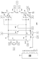
図2は、本発明の第2の実施形態に係るレベルシフト回路の構成の一例を示す図であり、図1と図2の同一符号は同一の構成を有する。
図2に示すレベルシフト回路は、図1に示すレベルシフト回路における電圧設定回路1として、p型MOSトランジスタQp2,Qp3と、n型MOSトランジスタQn2,Qn3,Qn4と、制御回路10とを有しており、他の構成については図1に示すレベルシフト回路と同じである。
FIG. 2 is a diagram showing an example of the configuration of the level shift circuit according to the second embodiment of the present invention, and the same reference numerals in FIGS. 1 and 2 have the same configuration.
The level shift circuit shown in FIG. 2 has p-type MOS transistors Qp2, Qp3, n-type MOS transistors Qn2, Qn3, Qn4, and a
図2に示すレベルシフト回路において、p型MOSトランジスタQp1を含む回路は、本発明の第1のスイッチの一実施形態である。
n型MOSトランジスタQn1を含む回路は、本発明の第2のスイッチの一実施形態である。
キャパシタCAは、本発明の第1のキャパシタの一実施形態である。
キャパシタCBは、本発明の第2のキャパシタの一実施形態である。
n型MOSトランジスタQn3およびQn4を含む回路は、本発明の第1の電圧供給回路の一実施形態である。
p型MOSトランジスタQp3を含む回路は、本発明の第2の電圧供給回路の一実施形態である。
p型MOSトランジスタQp2を含む回路は、本発明の第3のスイッチの一実施形態である。
n型MOSトランジスタQn2を含む回路は、本発明の第4のスイッチの一実施形態である。
In the level shift circuit shown in FIG. 2, the circuit including the p-type MOS transistor Qp1 is an embodiment of the first switch of the present invention.
The circuit including the n-type MOS transistor Qn1 is an embodiment of the second switch of the present invention.
Capacitor CA is an embodiment of the first capacitor of the present invention.
Capacitor CB is an embodiment of the second capacitor of the present invention.
A circuit including n-type MOS transistors Qn3 and Qn4 is an embodiment of the first voltage supply circuit of the present invention.
The circuit including the p-type MOS transistor Qp3 is an embodiment of the second voltage supply circuit of the present invention.
The circuit including the p-type MOS transistor Qp2 is an embodiment of the third switch of the present invention.
The circuit including the n-type MOS transistor Qn2 is an embodiment of the fourth switch of the present invention.
n型MOSトランジスタQn3は、ゲートに入力される制御信号S1に応じて、ノードNAに電圧‘VSS’を供給する。n型MOSトランジスタQn3は、ノードNAと電源ラインVSSとの間に接続されており、第1の期間(図3の時刻t1〜t2)においてオン状態に設定される。 The n-type MOS transistor Qn3 supplies the voltage 'VSS' to the node NA in response to the control signal S1 input to the gate. The n-type MOS transistor Qn3 is connected between the node NA and the power supply line VSS, and is set to an on state in the first period (time t1 to t2 in FIG. 3).
n型MOSトランジスタQn4は、ゲートに入力される制御信号S1に応じて、ノードNBに電圧‘VSS’を供給する。n型MOSトランジスタQn4は、ノードNBと電源ラインVSSとの間に接続されており、第1の期間(図3の時刻t1〜t2)においてオン状態になる。 The n-type MOS transistor Qn4 supplies the voltage 'VSS' to the node NB in response to the control signal S1 input to the gate. The n-type MOS transistor Qn4 is connected between the node NB and the power supply line VSS and is turned on in the first period (time t1 to t2 in FIG. 3).
p型MOSトランジスタQp2は、ゲートに入力される制御信号S2に応じて、p型MOSトランジスタQp1のドレインとノードNAとを接続または遮断するスイッチとして動作する。p型MOSトランジスタQp2は、第2の期間(図3の時刻t2〜t3)においてp型MOSトランジスタQp1のドレインとノードNAとを接続する。 The p-type MOS transistor Qp2 operates as a switch for connecting or disconnecting the drain of the p-type MOS transistor Qp1 and the node NA according to the control signal S2 input to the gate. The p-type MOS transistor Qp2 connects the drain of the p-type MOS transistor Qp1 and the node NA in the second period (time t2 to t3 in FIG. 3).
p型MOSトランジスタQp3は、ゲートに入力される制御信号S3に応じて、ノードNBに電圧‘VDD’を供給する。p型MOSトランジスタQp3は、ノードNBと電源ラインVDDとの間に接続されており、第3の期間(図3の時刻t3〜t4)においてオン状態に設定される。 The p-type MOS transistor Qp3 supplies the voltage “VDD” to the node NB in accordance with the control signal S3 input to the gate. The p-type MOS transistor Qp3 is connected between the node NB and the power supply line VDD, and is set to an on state in the third period (time t3 to t4 in FIG. 3).
n型MOSトランジスタQn2は、ゲートに入力される制御信号S4に応じてn型MOSトランジスタQn1のドレインとノードNBとを接続または遮断するスイッチとして動作する。n型MOSトランジスタQn2は、第4の期間(図3の時刻t4〜t5)において、n型MOSトランジスタQn1のドレインとノードNBとを接続する。 The n-type MOS transistor Qn2 operates as a switch that connects or disconnects the drain of the n-type MOS transistor Qn1 and the node NB according to the control signal S4 input to the gate. The n-type MOS transistor Qn2 connects the drain of the n-type MOS transistor Qn1 and the node NB in the fourth period (time t4 to t5 in FIG. 3).
制御回路10は、ノードNAおよびNBに適切な電圧が設定されるように、上述した制御信号S1〜S4を生成する。
すなわち、第1の期間(t1〜t2)において、制御信号S1を電圧‘VDD’に設定し、他の期間において、制御信号S1を電圧‘VSS’に設定する。
第1の期間に続く第2の期間(t2〜t3)において、制御信号S2を電圧‘VSS’に設定し、他の期間において、制御信号S2を電圧‘VDD’に設定する。
第2の期間に続く第3の期間(t3〜t4)において、制御信号S3を電圧‘VSS’に設定し、他の期間において、制御信号S3を電圧‘VDD’に設定する。
第3の期間に続く第4の期間(t4〜t5)において、制御信号S4を電圧‘VDD’に設定し、他の期間において、制御信号S4を電圧‘VSS’に設定する。
The
That is, the control signal S1 is set to the voltage 'VDD' in the first period (t1 to t2), and the control signal S1 is set to the voltage 'VSS' in the other periods.
In the second period (t2 to t3) following the first period, the control signal S2 is set to the voltage 'VSS', and in the other period, the control signal S2 is set to the voltage 'VDD'.
In the third period (t3 to t4) following the second period, the control signal S3 is set to the voltage 'VSS', and in the other period, the control signal S3 is set to the voltage 'VDD'.
In the fourth period (t4 to t5) following the third period, the control signal S4 is set to the voltage 'VDD', and in the other period, the control signal S4 is set to the voltage 'VSS'.
次に、上述した構成を有する図2に示すレベルシフト回路の動作について、図3を参照して説明する。 Next, the operation of the level shift circuit shown in FIG. 2 having the above-described configuration will be described with reference to FIG.
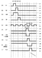
図3は、図2に示すレベルシフト回路における各部の信号波形の一例を示す図である。
図3(A)は、制御信号S1の電圧波形を示す。
図3(B)は、制御信号S2の電圧波形を示す。
図3(C)は、制御信号S3の電圧波形を示す。
図3(D)は、制御信号S4の電圧波形を示す。
図3(E)は、第1の入力信号IN1の電圧波形を示す。
図3(F)は、第2の入力信号IN2の電圧波形を示す。
図3(G)は、ノードNAの電圧V_NAの電圧波形を示す。
図3(H)は、ノードNBの電圧V_NBの電圧波形を示す。
図3(I)は、レベルシフト信号Oの電圧波形を示す。
FIG. 3 is a diagram showing an example of signal waveforms at various parts in the level shift circuit shown in FIG.
FIG. 3A shows a voltage waveform of the control signal S1.
FIG. 3B shows a voltage waveform of the control signal S2.
FIG. 3C shows a voltage waveform of the control signal S3.
FIG. 3D shows a voltage waveform of the control signal S4.
FIG. 3E shows a voltage waveform of the first input signal IN1.
FIG. 3F shows a voltage waveform of the second input signal IN2.
FIG. 3G shows a voltage waveform of the voltage V_NA at the node NA.
FIG. 3H illustrates a voltage waveform of the voltage V_NB of the node NB.
FIG. 3I shows the voltage waveform of the level shift signal O.
ノードNAおよびNBの電圧設定を行う前の初期の状態において、制御回路10は、制御信号S1およびS4を電圧‘VSS’、制御信号S2およびS3を電圧‘VDD’に設定する。この場合、電圧設定回路の各トランジスタ(Qp2,Qp3,Qn2,Qn3,Qn4)は全てオフする。
In an initial state before setting the voltages of the nodes NA and NB, the
また、この初期の状態において、第1の入力信号IN1は電圧‘Vin’に設定され、第2の入力信号IN2は電圧‘VSS’に設定される。なお、第1の入力信号IN1および第2の入力信号IN2は、電圧‘Vin’をハイレベル、電圧‘VSS’をローレベルとする2値の信号である。 In this initial state, the first input signal IN1 is set to the voltage 'Vin', and the second input signal IN2 is set to the voltage 'VSS'. The first input signal IN1 and the second input signal IN2 are binary signals in which the voltage ‘Vin’ is at a high level and the voltage ‘VSS’ is at a low level.
第1の期間(t1〜t2)において、制御回路10は制御信号S1を電圧‘VDD’に設定する。これにより、n型MOSトランジスタQn3がオンし、ノードNAは電圧‘VSS’に設定され、p型MOSトランジスタQp1はオンする。
In the first period (t1 to t2), the
このとき、n型MOSトランジスタQn4がオンし、ノードNBも電圧‘VSS’に設定されるため、n型MOSトランジスタQn1はオフする。
第1の期間(t1〜t2)においてn型MOSトランジスタQn1をオフすることにより、p型MOSトランジスタQp1およびn型MOSトランジスタQn1が同時にオンすることによる貫通電流の発生を防止することができる。
At this time, the n-type MOS transistor Qn4 is turned on and the node NB is also set to the voltage 'VSS', so that the n-type MOS transistor Qn1 is turned off.
By turning off the n-type MOS transistor Qn1 in the first period (t1 to t2), it is possible to prevent the occurrence of a through current due to the p-type MOS transistor Qp1 and the n-type MOS transistor Qn1 being turned on simultaneously.
ノードNAが電圧‘VSS’に設定された後の第2の期間(t2〜t3)において、制御回路10は制御信号S1を電圧‘VSS’に戻し、制御信号S2を電圧‘VSS’に立ち下げる。これにより、p型MOSトランジスタQp2がオンし、ノードNAとp型MOSトランジスタQp1のドレインとが接続される。
このとき、p型MOSトランジスタQp1はオン状態にあり、電源ラインVDDからp型MOSトランジスタQp1を介してノードNAに電流が流れるため、ノードNAの電圧V_NAは電圧‘VDD’に向かって上昇する。
電圧V_NAが‘VDD−Vthp’に達すると、p型MOSトランジスタQp1が自らオフするため、電圧V_NAの上昇は停止する。その結果、ノードNAの電圧V_NAは‘VDD−Vthp’に設定される。
In the second period (t2 to t3) after the node NA is set to the voltage 'VSS', the
At this time, the p-type MOS transistor Qp1 is in an on state, and a current flows from the power supply line VDD to the node NA via the p-type MOS transistor Qp1, so that the voltage V_NA of the node NA rises toward the voltage 'VDD'.
When the voltage V_NA reaches “VDD−Vthp”, the p-type MOS transistor Qp1 is turned off by itself, and the increase in the voltage V_NA is stopped. As a result, the voltage V_NA of the node NA is set to “VDD−Vthp”.
p型MOSトランジスタQp1がオフした後の第3の期間(t3〜t4)において、制御回路10は制御信号S2を電圧‘VDD’に戻し、制御信号S3を電圧‘VSS’に立ち下げる。これにより、p型MOSトランジスタQp3がオンし、ノードNBは電圧‘VDD’に設定され、n型MOSトランジスタQn1はオンする。
In the third period (t3 to t4) after the p-type MOS transistor Qp1 is turned off, the
なお、このときp型MOSトランジスタQp1はオフ状態にあるため、n型MOSトランジスタQn1がオンに変化しても、両者を貫通する電流は流れない。 At this time, since the p-type MOS transistor Qp1 is in an off state, even if the n-type MOS transistor Qn1 is turned on, a current passing through both does not flow.
ノードNBが電圧‘VDD’に設定された後の第4の期間(t4〜t5)において、制御回路10は制御信号S3を電圧‘VDD’に戻し、制御信号S4を電圧‘VDD’に立ち上げる。これにより、n型MOSトランジスタQn2がオンし、ノードNBとn型MOSトランジスタQn1のドレインとが接続される。
このとき、n型MOSトランジスタQn1はオン状態にあり、ノードNBからn型MOSトランジスタQn1を介して電源ラインVSSに電流が流れるため、ノードNBの電圧V_NBは電圧‘VSS’に向かって低下する。
電圧V_NBが‘VSS+Vthn’に達すると、n型MOSトランジスタQn1が自らオフするため、電圧V_NBの低下は停止する。その結果、ノードNBの電圧V_NBは‘VSS+Vthn’に設定される。
In the fourth period (t4 to t5) after the node NB is set to the voltage 'VDD', the
At this time, the n-type MOS transistor Qn1 is in an on state, and a current flows from the node NB to the power supply line VSS via the n-type MOS transistor Qn1, so that the voltage V_NB of the node NB decreases toward the voltage 'VSS'.
When the voltage V_NB reaches 'VSS + Vthn', the n-type MOS transistor Qn1 is turned off by itself, so that the decrease of the voltage V_NB stops. As a result, the voltage V_NB of the node NB is set to “VSS + Vthn”.
ノードNAの電圧V_NAが‘VDD−Vthp’、ノードNBの電圧V_NBが‘VSS+Vthn’に設定された後、第1の入力信号IN1および第2の入力信号IN2は同相に変化する(時刻t6以降)。
例えば時刻t6〜t7において、第1の入力信号IN1および第2の入力信号IN2がローレベル(VSS)になり、電圧V_NAは‘VDD−Vthp−Vin’、電圧V_NBは‘VSS+Vthn’になる。これにより、p型MOSトランジスタQp1がオン、n型MOSトランジスタQn1がオフするため、レベルシフト信号Oは電圧‘VDD’になる。
また、例えば時刻t7〜t8において、第1の入力信号IN1および第2の入力信号IN2がハイレベル(Vin)になり、電圧V_NAは‘VDD−Vthp’、電圧V_NBは‘VSS+Vthn+Vin’になる。これにより、n型MOSトランジスタQn1がオン、p型MOSトランジスタQp1がオフするため、レベルシフト信号Oは電圧‘VSS’になる。
After the voltage V_NA of the node NA is set to “VDD−Vthp” and the voltage V_NB of the node NB is set to “VSS + Vthn”, the first input signal IN1 and the second input signal IN2 change in phase (after time t6). .
For example, from time t6 to t7, the first input signal IN1 and the second input signal IN2 are at a low level (VSS), the voltage V_NA is 'VDD-Vthp-Vin', and the voltage V_NB is 'VSS + Vthn'. As a result, the p-type MOS transistor Qp1 is turned on and the n-type MOS transistor Qn1 is turned off, so that the level shift signal O becomes the voltage 'VDD'.
Further, for example, from time t7 to t8, the first input signal IN1 and the second input signal IN2 are at a high level (Vin), the voltage V_NA is 'VDD-Vthp', and the voltage V_NB is 'VSS + Vthn + Vin'. As a result, the n-type MOS transistor Qn1 is turned on and the p-type MOS transistor Qp1 is turned off, so that the level shift signal O becomes the voltage 'VSS'.
以上説明したように、本実施形態に係るレベルシフト回路によれば、ノードNAの電圧が‘VDD−Vthp’に設定され、ノードNBの電圧が‘VSS+Vthn’に設定されるため、トランジスタ(Qp1,Qn1)のしきい電圧のばらつきに影響されることなく、安定したレベルシフト動作を行うことができる。
また、ノードNAおよびNBの電圧設定期間(t1〜t5)やレベルシフト動作の期間において、p型MOSトランジスタQp1およびn型MOSトランジスタQn1が同時にオンすることを防止できるため、レベルシフト動作に伴うリーク電流を抑制し、消費電力を小さくすることができる。
更に、ノードNAおよびNBの電圧が、p型MOSトランジスタQp1およびn型MOSトランジスタQn1のオン/オフの切り換わり点の電圧にそれぞれ設定されるため、トランジスタのしきい電圧より小さい振幅の信号であってもレベルシフト動作が可能であり、信号の変換範囲を広くすることができる。
As described above, according to the level shift circuit of this embodiment, the voltage at the node NA is set to “VDD−Vthp” and the voltage at the node NB is set to “VSS + Vthn”. A stable level shift operation can be performed without being affected by variations in the threshold voltage of Qn1).
Further, since it is possible to prevent the p-type MOS transistor Qp1 and the n-type MOS transistor Qn1 from being turned on at the same time during the voltage setting period (t1 to t5) of the nodes NA and NB and the period of the level shift operation, there is a leakage caused by the level shift operation. Current can be suppressed and power consumption can be reduced.
Furthermore, since the voltages at the nodes NA and NB are set to the voltages at the on / off switching points of the p-type MOS transistor Qp1 and the n-type MOS transistor Qn1, respectively, the signal has an amplitude smaller than the threshold voltage of the transistor. However, the level shift operation is possible, and the signal conversion range can be widened.
<第3の実施形態>
次に、本発明の第3の実施形態について説明する。
第2の実施形態に係るレベルシフト回路(図2)では、高電位側のノードNAの電圧設定を行った後に低電位側のノードNBの電圧設定を行うが、本実施形態に係るレベルシフト回路(図4)では、低電位側のノードNBの電圧設定を行った後に高電位側のノードNAの電圧設定を行う。
<Third Embodiment>
Next, a third embodiment of the present invention will be described.
In the level shift circuit according to the second embodiment (FIG. 2), the voltage of the node NB on the low potential side is set after the voltage of the node NA on the high potential side is set. The level shift circuit according to the present embodiment In FIG. 4, after setting the voltage of the node NB on the low potential side, the voltage of the node NA on the high potential side is set.
図4は、本発明の第3の実施形態に係るレベルシフト回路の構成の一例を示す図であり、図1と図3の同一符号は同一の構成を有する。
図4に示すレベルシフト回路は、図1に示すレベルシフト回路における電圧設定回路1として、p型MOSトランジスタQp2,Qp3,Qp4と、n型MOSトランジスタQn2,Qn3と、制御回路10Aとを有しており、他の構成については図1に示すレベルシフト回路と同じである。
FIG. 4 is a diagram showing an example of the configuration of the level shift circuit according to the third embodiment of the present invention. The same reference numerals in FIGS. 1 and 3 have the same configuration.
The level shift circuit shown in FIG. 4 has p-type MOS transistors Qp2, Qp3, Qp4, n-type MOS transistors Qn2, Qn3, and a
図4に示すレベルシフト回路において、n型MOSトランジスタQn1を含む回路は、本発明の第1のスイッチの一実施形態である。
p型MOSトランジスタQp1を含む回路は、本発明の第2のスイッチの一実施形態である。
キャパシタCBは、本発明の第1のキャパシタの一実施形態である。
キャパシタCAは、本発明の第2のキャパシタの一実施形態である。
p型MOSトランジスタQp3およびQp4を含む回路は、本発明の第1の電圧供給回路の一実施形態である。
n型MOSトランジスタQn3を含む回路は、本発明の第2の電圧供給回路の一実施形態である。
n型MOSトランジスタQn2を含む回路は、本発明の第3のスイッチの一実施形態である。
p型MOSトランジスタQp2を含む回路は、本発明の第4のスイッチの一実施形態である。
In the level shift circuit shown in FIG. 4, the circuit including the n-type MOS transistor Qn1 is an embodiment of the first switch of the present invention.
The circuit including the p-type MOS transistor Qp1 is an embodiment of the second switch of the present invention.
Capacitor CB is an embodiment of the first capacitor of the present invention.
Capacitor CA is an embodiment of the second capacitor of the present invention.
A circuit including p-type MOS transistors Qp3 and Qp4 is an embodiment of the first voltage supply circuit of the present invention.
The circuit including the n-type MOS transistor Qn3 is an embodiment of the second voltage supply circuit of the present invention.
The circuit including the n-type MOS transistor Qn2 is an embodiment of the third switch of the present invention.
The circuit including the p-type MOS transistor Qp2 is an embodiment of the fourth switch of the present invention.
p型MOSトランジスタQp3は、ゲートに入力される制御信号S3に応じて、ノードNBに電圧‘VDD’を供給する。p型MOSトランジスタQp3は、ノードNBと電源ラインVDDとの間に接続されており、第1の期間(図5の時刻t11〜t12)においてオン状態に設定される。 The p-type MOS transistor Qp3 supplies the voltage “VDD” to the node NB in accordance with the control signal S3 input to the gate. The p-type MOS transistor Qp3 is connected between the node NB and the power supply line VDD, and is set to an on state in the first period (time t11 to t12 in FIG. 5).
p型MOSトランジスタQp4は、ゲートに入力される制御信号S3に応じて、ノードNAに電圧‘VDD’を供給する。p型MOSトランジスタQp4は、ノードNAと電源ラインVDDとの間に接続されており、第1の期間(図5の時刻t11〜t12)においてオン状態に設定される。 The p-type MOS transistor Qp4 supplies the voltage “VDD” to the node NA in accordance with the control signal S3 input to the gate. The p-type MOS transistor Qp4 is connected between the node NA and the power supply line VDD, and is set to an on state in the first period (time t11 to t12 in FIG. 5).
n型MOSトランジスタQn2は、ゲートに入力される制御信号S4に応じて、n型MOSトランジスタQn1のドレインとノードNBとを接続または遮断するスイッチとして動作する。n型MOSトランジスタQn2は、第2の期間(図5の時刻t12〜t13)において、n型MOSトランジスタQn1のドレインとノードNBとを接続する。 The n-type MOS transistor Qn2 operates as a switch for connecting or disconnecting the drain of the n-type MOS transistor Qn1 and the node NB according to the control signal S4 input to the gate. The n-type MOS transistor Qn2 connects the drain of the n-type MOS transistor Qn1 and the node NB in the second period (time t12 to t13 in FIG. 5).
n型MOSトランジスタQn3は、ゲートに入力される制御信号S1に応じて、ノードNAに電圧‘VSS’を供給する。n型MOSトランジスタQn3は、ノードNAと電源ラインVSSとの間に接続されており、第3の期間(図5の時刻t13〜t14)においてオン状態に設定される。 The n-type MOS transistor Qn3 supplies the voltage 'VSS' to the node NA in response to the control signal S1 input to the gate. The n-type MOS transistor Qn3 is connected between the node NA and the power supply line VSS, and is set to an on state in the third period (time t13 to t14 in FIG. 5).
p型MOSトランジスタQp2は、ゲートに入力される制御信号S2に応じて、p型MOSトランジスタQp1のドレインとノードNAとを接続または遮断するスイッチとして動作する。p型MOSトランジスタQp2は、第4の期間(図5の時刻t14〜t15)において、p型MOSトランジスタQp1のドレインとノードNAを接続する。 The p-type MOS transistor Qp2 operates as a switch for connecting or disconnecting the drain of the p-type MOS transistor Qp1 and the node NA according to the control signal S2 input to the gate. The p-type MOS transistor Qp2 connects the drain of the p-type MOS transistor Qp1 and the node NA in the fourth period (time t14 to t15 in FIG. 5).
制御回路10Aは、ノードNAおよびNBに適切な電圧が設定されるように、上述した制御信号S1〜S4を生成する。
すなわち、第1の期間(t11〜t12)において、制御信号S3を電圧‘VSS’に設定し、他の期間において、制御信号S3を電圧‘VDD’に設定する。
第1の期間に続く第2の期間(t12〜t13)において、制御信号S4を電圧‘VDD’に設定し、他の期間において、制御信号S4を電圧‘VSS’に設定する。
第2の期間に続く第3の期間(t13〜t14)において、制御信号S1を電圧‘VDD’に設定し、他の期間において、制御信号S1を電圧‘VSS’に設定する。
第3の期間に続く第4の期間(t14〜t15)において、制御信号S2を電圧‘VSS’に設定し、他の期間において、制御信号S2を電圧‘VDD’に設定する。
The
That is, the control signal S3 is set to the voltage 'VSS' in the first period (t11 to t12), and the control signal S3 is set to the voltage 'VDD' in the other periods.
In the second period (t12 to t13) following the first period, the control signal S4 is set to the voltage 'VDD', and in the other period, the control signal S4 is set to the voltage 'VSS'.
In the third period (t13 to t14) following the second period, the control signal S1 is set to the voltage 'VDD', and in the other period, the control signal S1 is set to the voltage 'VSS'.
In the fourth period (t14 to t15) following the third period, the control signal S2 is set to the voltage 'VSS', and in the other period, the control signal S2 is set to the voltage 'VDD'.
次に、上述した構成を有する図4に示すレベルシフト回路の動作について、図5を参照して説明する。 Next, the operation of the level shift circuit shown in FIG. 4 having the above-described configuration will be described with reference to FIG.
図5は、図4に示すレベルシフト回路における各部の信号波形の一例を示す図である。
図5(A)〜(I)の信号波形は、図3(A)〜(I)の信号波形に対応する。
FIG. 5 is a diagram showing an example of signal waveforms at various parts in the level shift circuit shown in FIG.
The signal waveforms in FIGS. 5A to 5I correspond to the signal waveforms in FIGS.
ノードNAおよびNBの電圧設定を行う前の初期の状態において、制御回路10Aは制御信号S1およびS4を電圧‘VSS’、制御信号S2およびS3を電圧‘VDD’に設定し、電圧設定回路の各トランジスタ(Qp2,Qp3,Qp4,Qn2,Qn3)を全てオフさせる。
また、この初期の状態において、第1の入力信号IN1はハイレベルの電圧‘Vin’に設定され、第2の入力信号IN2はローレベルの電圧‘VSS’に設定される。
In the initial state before setting the voltages of the nodes NA and NB, the
In this initial state, the first input signal IN1 is set to the high level voltage 'Vin', and the second input signal IN2 is set to the low level voltage 'VSS'.
第1の期間(t1〜t2)において、制御回路10Aは制御信号S3を電圧‘VSS’に設定する。これにより、p型MOSトランジスタQp3がオンし、ノードNBは電圧‘VDD’に設定され、n型MOSトランジスタQn1はオンする。
In the first period (t1 to t2), the
このとき、p型MOSトランジスタQp4がオンし、ノードNAも電圧‘VDD’に設定されるため、p型MOSトランジスタQp1はオフする。
第1の期間(t11〜t12)においてp型MOSトランジスタQp1をオフすることにより、p型MOSトランジスタQp1およびn型MOSトランジスタQn1が同時にオンすることによる貫通電流の発生を防止することができる。
At this time, the p-type MOS transistor Qp4 is turned on and the node NA is also set to the voltage 'VDD', so that the p-type MOS transistor Qp1 is turned off.
By turning off the p-type MOS transistor Qp1 in the first period (t11 to t12), it is possible to prevent the occurrence of a through current due to the p-type MOS transistor Qp1 and the n-type MOS transistor Qn1 being simultaneously turned on.
ノードNBが電圧‘VDD’に設定された後の第2の期間(t12〜t13)において、制御回路10Aは制御信号S3を電圧‘VDD’に戻し、制御信号S4を電圧‘VDD’に立ち上げる。これにより、n型MOSトランジスタQn2がオンし、n型MOSトランジスタQn1のドレインとノードNBとが接続される。
このとき、n型MOSトランジスタQn1はオン状態にあり、ノードNBからn型MOSトランジスタQn1を介して電源ラインVSSに電流が流れるため、ノードNBの電圧V_NBは電圧‘VSS’に向かって低下する。
電圧V_NBが‘VSS+Vthn’に達すると、n型MOSトランジスタQn1が自らオフするため、電圧V_NBの低下は停止する。その結果、ノードNBの電圧V_NBは‘VSS+Vthn’に設定される。
In the second period (t12 to t13) after the node NB is set to the voltage 'VDD', the
At this time, the n-type MOS transistor Qn1 is in an on state, and a current flows from the node NB to the power supply line VSS via the n-type MOS transistor Qn1, so that the voltage V_NB of the node NB decreases toward the voltage 'VSS'.
When the voltage V_NB reaches 'VSS + Vthn', the n-type MOS transistor Qn1 is turned off by itself, so that the decrease of the voltage V_NB stops. As a result, the voltage V_NB of the node NB is set to “VSS + Vthn”.
n型MOSトランジスタQn1がオフした後の第3の期間(t13〜t14)において、制御回路10Aは制御信号S4を電圧‘VSS’に戻し、制御信号S1を電圧‘VDD’に立ち上げる。これにより、n型MOSトランジスタQn3がオンし、ノードNAは電圧‘VSS’に設定され、p型MOSトランジスタQp1はオンする。
In the third period (t13 to t14) after the n-type MOS transistor Qn1 is turned off, the
なお、このときn型MOSトランジスタQn1はオフ状態にあるため、p型MOSトランジスタQp1がオンに変化しても、両者を貫通する電流は流れない。 At this time, since the n-type MOS transistor Qn1 is in an off state, even if the p-type MOS transistor Qp1 is turned on, a current passing through both does not flow.
ノードNAが電圧‘VSS’に設定された後の第4の期間(t14〜t15)において、制御回路10Aは制御信号S1を電圧‘VSS’に戻し、制御信号S2を電圧‘VSS’に立ち下げる。これにより、p型MOSトランジスタQp2がオンし、p型MOSトランジスタQp1のドレインとノードNAとが接続される。
このとき、p型MOSトランジスタQp1はオン状態にあり、電源ラインVDDからp型MOSトランジスタQp1を介してノードNAに電流が流れるため、ノードNAの電圧V_NAは電圧‘VDD’に向かって上昇する。
電圧V_NAが‘VDD−Vthp’に達すると、p型MOSトランジスタQp1が自らオフするため、電圧V_NAの上昇は停止する。その結果、ノードNAの電圧V_NAは‘VDD−Vthp’に設定される。
In the fourth period (t14 to t15) after the node NA is set to the voltage 'VSS', the
At this time, the p-type MOS transistor Qp1 is in an on state, and a current flows from the power supply line VDD to the node NA via the p-type MOS transistor Qp1, so that the voltage V_NA of the node NA rises toward the voltage 'VDD'.
When the voltage V_NA reaches “VDD−Vthp”, the p-type MOS transistor Qp1 is turned off by itself, and the increase in the voltage V_NA is stopped. As a result, the voltage V_NA of the node NA is set to “VDD−Vthp”.
ノードNAの電圧V_NAが‘VDD−Vthp’、ノードNBの電圧V_NBが‘VSS+Vthn’に設定された後の動作については、図2に示すレベルシフト回路と同様である。
例えば時刻t16〜t17において、第1の入力信号IN1および第2の入力信号IN2がローレベル(VSS)になると、p型MOSトランジスタQp1がオン、n型MOSトランジスタQn1がオフし、レベルシフト信号Oは電圧‘VDD’になる。
また、例えば時刻t17〜t18において、第1の入力信号IN1および第2の入力信号IN2がハイレベル(Vin)になると、n型MOSトランジスタQn1がオン、p型MOSトランジスタQp1がオフし、レベルシフト信号Oは電圧‘VSS’になる。
The operation after the voltage V_NA of the node NA is set to “VDD−Vthp” and the voltage V_NB of the node NB is set to “VSS + Vthn” is the same as that of the level shift circuit shown in FIG.
For example, at time t16 to t17, when the first input signal IN1 and the second input signal IN2 become low level (VSS), the p-type MOS transistor Qp1 is turned on, the n-type MOS transistor Qn1 is turned off, and the level shift signal O Becomes the voltage 'VDD'.
Also, for example, at time t17 to t18, when the first input signal IN1 and the second input signal IN2 become high level (Vin), the n-type MOS transistor Qn1 is turned on, the p-type MOS transistor Qp1 is turned off, and the level shift is performed. The signal O becomes the voltage 'VSS'.
以上説明したように、本実施形態に係るレベルシフト回路においても、図2に示すレベルシフト回路と同様な動作が実現されるため、これと同様な効果を奏することができる。
すなわち、ノードNAの電圧が‘VDD−Vthp’、ノードNBの電圧が‘VSS+Vthn’に設定されるため、トランジスタ(Qp1,Qn1)のしきい電圧のばらつきに影響されることなく、安定したレベルシフト動作を行うことができる。
また、p型MOSトランジスタQp1およびn型MOSトランジスタQn1が同時にオンすることを防止できるため、レベルシフト動作に伴うリーク電流を抑制できる。
また、ノードNAおよびNBの電圧が、p型MOSトランジスタQp1およびn型MOSトランジスタQn1のオン/オフの切り換わり点の電圧にそれぞれ設定されるため、トランジスタのしきい電圧より小さい振幅の信号であってもレベルシフト動作が可能である。
As described above, in the level shift circuit according to this embodiment, the same operation as that of the level shift circuit shown in FIG. 2 is realized, so that the same effect can be obtained.
That is, since the voltage at the node NA is set to “VDD−Vthp” and the voltage at the node NB is set to “VSS + Vthn”, the level shift is stable without being affected by variations in the threshold voltages of the transistors (Qp1, Qn1). The action can be performed.
Further, since it is possible to prevent the p-type MOS transistor Qp1 and the n-type MOS transistor Qn1 from being turned on at the same time, it is possible to suppress the leakage current accompanying the level shift operation.
Further, since the voltages at nodes NA and NB are set to the voltages at the on / off switching points of p-type MOS transistor Qp1 and n-type MOS transistor Qn1, respectively, the signals have amplitudes smaller than the threshold voltage of the transistor. Even level shift operation is possible.
<第4の実施形態>
次に、本発明の第4の実施形態について説明する。
第2および第3の実施形態に係るレベルシフト回路では、p型MOSトランジスタQp1およびn型MOSトランジスタQn1が同時にオンすることによる貫通電流の発生を防ぐため、ノードNAおよびNBの電圧設定が別々に行われているが、本実施形態に係るレベルシフト回路では、両者の電圧設定を並行に行う。
<Fourth Embodiment>
Next, a fourth embodiment of the present invention will be described.
In the level shift circuits according to the second and third embodiments, the voltage settings of the nodes NA and NB are separately set in order to prevent the occurrence of a through current due to the p-type MOS transistor Qp1 and the n-type MOS transistor Qn1 being simultaneously turned on. However, in the level shift circuit according to the present embodiment, both voltage settings are performed in parallel.
図6は、本発明の第4の実施形態に係るレベルシフト回路の構成の一例を示す図であり、図1と図6の同一符号は同一の構成を有する。
図6に示すレベルシフト回路は、図1に示すレベルシフト回路における電圧設定回路1として、p型MOSトランジスタQp2,Qp3,Qp5と、n型MOSトランジスタQn2,Qn3,Qn5と、制御回路10Bとを有しており、他の構成については図1に示すレベルシフト回路と同じである。
FIG. 6 is a diagram showing an example of the configuration of the level shift circuit according to the fourth embodiment of the present invention. The same reference numerals in FIGS. 1 and 6 have the same configuration.
The level shift circuit shown in FIG. 6 includes, as
図6に示すレベルシフト回路において、p型MOSトランジスタQp1を含む回路は、本発明の第1のスイッチの一実施形態である。
n型MOSトランジスタQn1を含む回路は、本発明の第2のスイッチの一実施形態である。
キャパシタCAは、本発明の第1のキャパシタの一実施形態である。
キャパシタCBは、本発明の第2のキャパシタの一実施形態である。
n型MOSトランジスタQn3を含む回路は、本発明の第1の電圧供給回路の一実施形態である。
p型MOSトランジスタQp3を含む回路は、本発明の第2の電圧供給回路の一実施形態である。
p型MOSトランジスタQp2を含む回路は、本発明の第3のスイッチの一実施形態である。
n型MOSトランジスタQn2を含む回路は、本発明の第4のスイッチの一実施形態である。
p型MOSトランジスタQp5およびn型MOSトランジスタQn5を含む回路は、本発明の第5のスイッチの一実施形態である。
In the level shift circuit shown in FIG. 6, the circuit including the p-type MOS transistor Qp1 is an embodiment of the first switch of the present invention.
The circuit including the n-type MOS transistor Qn1 is an embodiment of the second switch of the present invention.
Capacitor CA is an embodiment of the first capacitor of the present invention.
Capacitor CB is an embodiment of the second capacitor of the present invention.
The circuit including the n-type MOS transistor Qn3 is an embodiment of the first voltage supply circuit of the present invention.
The circuit including the p-type MOS transistor Qp3 is an embodiment of the second voltage supply circuit of the present invention.
The circuit including the p-type MOS transistor Qp2 is an embodiment of the third switch of the present invention.
The circuit including the n-type MOS transistor Qn2 is an embodiment of the fourth switch of the present invention.
A circuit including the p-type MOS transistor Qp5 and the n-type MOS transistor Qn5 is an embodiment of the fifth switch of the present invention.
n型MOSトランジスタQn3は、ゲートに入力される制御信号S1に応じて、ノードNAに電圧‘VSS’を供給する。n型MOSトランジスタQn3は、ノードNAと電源ラインVSSとの間に接続されており、第1の期間(図7の時刻t21〜t22)においてオン状態に設定される。 The n-type MOS transistor Qn3 supplies the voltage 'VSS' to the node NA in response to the control signal S1 input to the gate. The n-type MOS transistor Qn3 is connected between the node NA and the power supply line VSS, and is set to an on state in the first period (time t21 to t22 in FIG. 7).
p型MOSトランジスタQp2は、ゲートに入力される制御信号S2に応じて、p型MOSトランジスタQp1のドレインとノードNAとを接続または遮断するスイッチとして動作する。p型MOSトランジスタQp2は、第2の期間(図7の時刻t22〜t23)において、p型MOSトランジスタQp1のドレインとノードNAとを接続する。 The p-type MOS transistor Qp2 operates as a switch for connecting or disconnecting the drain of the p-type MOS transistor Qp1 and the node NA according to the control signal S2 input to the gate. The p-type MOS transistor Qp2 connects the drain of the p-type MOS transistor Qp1 and the node NA in the second period (time t22 to t23 in FIG. 7).
p型MOSトランジスタQp3は、ゲートに入力される制御信号S3に応じて、ノードNBに電圧‘VDD’を供給する。p型MOSトランジスタQp3は、ノードNBと電源ラインVDDとの間に接続されており、第1の期間(図7の時刻t21〜t22)においてオン状態に設定される。 The p-type MOS transistor Qp3 supplies the voltage “VDD” to the node NB in accordance with the control signal S3 input to the gate. The p-type MOS transistor Qp3 is connected between the node NB and the power supply line VDD, and is set to an on state in the first period (time t21 to t22 in FIG. 7).
n型MOSトランジスタQn2は、ゲートに入力される制御信号S4に応じて、n型MOSトランジスタQn1のドレインとノードNBとを接続または遮断するスイッチとして動作する。n型MOSトランジスタQn2は、第2の期間(図7の時刻t22〜t23)において、n型MOSトランジスタQn1のドレインとノードNBとを接続する。 The n-type MOS transistor Qn2 operates as a switch for connecting or disconnecting the drain of the n-type MOS transistor Qn1 and the node NB according to the control signal S4 input to the gate. The n-type MOS transistor Qn2 connects the drain of the n-type MOS transistor Qn1 and the node NB in the second period (time t22 to t23 in FIG. 7).
p型MOSトランジスタQp5は、ゲートに入力される制御信号S5に応じて、p型MOSトランジスタQp1のドレインとレベルシフト信号Oの出力端子とを接続または遮断するスイッチとして動作する。p型MOSトランジスタQp5は、第1の期間および第2の期間(図7のt21〜t23)において、オフ状態に設定される。 The p-type MOS transistor Qp5 operates as a switch that connects or disconnects the drain of the p-type MOS transistor Qp1 and the output terminal of the level shift signal O in accordance with the control signal S5 input to the gate. The p-type MOS transistor Qp5 is set to an off state in the first period and the second period (t21 to t23 in FIG. 7).
n型MOSトランジスタQn5は、ゲートに入力される制御信号S6に応じて、n型MOSトランジスタQn1のドレインとレベルシフト信号Oの出力端子とを接続または遮断するスイッチとして動作する。n型MOSトランジスタQn5は、第1の期間および第2の期間(図7のt21〜t23)において、オフ状態に設定される。 The n-type MOS transistor Qn5 operates as a switch that connects or disconnects the drain of the n-type MOS transistor Qn1 and the output terminal of the level shift signal O in accordance with the control signal S6 input to the gate. The n-type MOS transistor Qn5 is set to an off state in the first period and the second period (t21 to t23 in FIG. 7).
制御回路10Bは、ノードNAおよびNBに適切な電圧が設定されるように、上述した制御信号S1〜S6を生成する。
すなわち、第1の期間(t21〜t22)において、制御信号S1を電圧‘VDD’、制御信号S3を電圧‘VSS’に設定し、他の期間において、制御信号S1を電圧‘VSS’、制御信号S3を電圧‘VDD’に設定する。制御信号S1およびS3は逆相の信号となる。
また、第1の期間に続く第2の期間(t22〜t23)において、制御信号S2を電圧‘VSS’、制御信号S4を電圧‘VDD’に設定し、他の期間において、制御信号S2を電圧‘VDD’、制御信号S4を電圧‘VSS’に設定する。制御信号S2およびS4は逆相の信号となる。
更に、第1の期間および第2の期間(t21〜t23)において、制御信号S5を電圧‘VDD’、制御信号S6を電圧‘VSS’に設定し、他の期間において、制御信号S5を電圧‘VSS’、制御信号S6を電圧‘VDD’に設定する。制御信号S5およびS6は逆相の信号となる。
The control circuit 10B generates the control signals S1 to S6 described above so that appropriate voltages are set to the nodes NA and NB.
That is, in the first period (t21 to t22), the control signal S1 is set to the voltage 'VDD' and the control signal S3 is set to the voltage 'VSS', and in the other period, the control signal S1 is set to the voltage 'VSS' and the control signal. S3 is set to voltage 'VDD'. The control signals S1 and S3 are reverse phase signals.
Further, in the second period (t22 to t23) following the first period, the control signal S2 is set to the voltage 'VSS', the control signal S4 is set to the voltage 'VDD', and the control signal S2 is set to the voltage in the other period. 'VDD' and control signal S4 are set to voltage 'VSS'. The control signals S2 and S4 are opposite phase signals.
Further, in the first period and the second period (t21 to t23), the control signal S5 is set to the voltage 'VDD', the control signal S6 is set to the voltage 'VSS', and in the other periods, the control signal S5 is set to the voltage ' VSS 'and control signal S6 are set to voltage' VDD '. The control signals S5 and S6 are opposite phase signals.
次に、上述した構成を有する図6に示すレベルシフト回路の動作について、図7を参照して説明する。 Next, the operation of the level shift circuit shown in FIG. 6 having the above-described configuration will be described with reference to FIG.
図7は、図6に示すレベルシフト回路における各部の信号波形の一例を示す図である。
図7(A)は、制御信号S3の電圧波形を示す。
図7(B)は、制御信号S2の電圧波形を示す。
図7(C)は、制御信号S5の電圧波形を示す。
図7(D)〜(H)の信号波形は、図3(E)〜(I)の信号波形に対応する。
FIG. 7 is a diagram showing an example of signal waveforms at various parts in the level shift circuit shown in FIG.
FIG. 7A shows a voltage waveform of the control signal S3.
FIG. 7B shows a voltage waveform of the control signal S2.
FIG. 7C shows the voltage waveform of the control signal S5.
The signal waveforms in FIGS. 7D to 7H correspond to the signal waveforms in FIGS.
なお、制御信号S1の電圧波形は、図7(A)に示す制御信号S3に対して逆相になる。
制御信号S4の電圧波形は、図7(B)に示す制御信号S2に対して逆相になる。
制御信号S6の電圧波形は、図7(C)に示す制御信号S5に対して逆相になる。
Note that the voltage waveform of the control signal S1 is opposite in phase to the control signal S3 shown in FIG.
The voltage waveform of the control signal S4 is opposite in phase to the control signal S2 shown in FIG.
The voltage waveform of the control signal S6 has a phase opposite to that of the control signal S5 shown in FIG.
ノードNAおよびNBの電圧設定を行う前の初期の状態において、制御回路10Bは制御信号S1およびS4を電圧‘VSS’、制御信号S2およびS3を電圧‘VDD’に設定し、トランジスタQp2,Qp3,Qn2,Qn3をオフさせる。
また、この初期の状態において、第1の入力信号IN1はハイレベルの電圧‘Vin’に設定され、第2の入力信号IN2はローレベルの電圧‘VSS’に設定される。
In an initial state before setting the voltages of the nodes NA and NB, the control circuit 10B sets the control signals S1 and S4 to the voltage 'VSS', the control signals S2 and S3 to the voltage 'VDD', and the transistors Qp2, Qp3 Qn2 and Qn3 are turned off.
In this initial state, the first input signal IN1 is set to the high level voltage 'Vin', and the second input signal IN2 is set to the low level voltage 'VSS'.
第1の期間(t21〜t22)において、制御回路10Bは制御信号S1を電圧‘VDD’に設定し、制御信号S3を電圧‘VSS’に設定する。これにより、n型MOSトランジスタQn3およびp型MOSトランジスタQp3が共にオンし、ノードNAが電圧‘VSS’、ノードNBが電圧‘VDD’に設定される。これにより、p型MOSトランジスタQp1およびn型MOSトランジスタQn1が共にオンする。
一方、このとき制御回路10Bは制御信号S5を電圧‘VDD’、制御信号S6を電圧‘VSS’に設定するため、p型MOSトランジスタQp5およびn型MOSトランジスタQn5が共にオフする。そのため、p型MOSトランジスタQp1およびn型MOSトランジスタQn1が同時にオンしても、貫通電流は流れない。
In the first period (t21 to t22), the control circuit 10B sets the control signal S1 to the voltage 'VDD', and sets the control signal S3 to the voltage 'VSS'. As a result, both n-type MOS transistor Qn3 and p-type MOS transistor Qp3 are turned on, node NA is set to voltage 'VSS', and node NB is set to voltage 'VDD'. Thereby, both p-type MOS transistor Qp1 and n-type MOS transistor Qn1 are turned on.
On the other hand, since the control circuit 10B sets the control signal S5 to the voltage 'VDD' and the control signal S6 to the voltage 'VSS' at this time, both the p-type MOS transistor Qp5 and the n-type MOS transistor Qn5 are turned off. Therefore, even if the p-type MOS transistor Qp1 and the n-type MOS transistor Qn1 are simultaneously turned on, no through current flows.
ノードNAが電圧‘VSS’、ノードNBが電圧‘VDD’に設定された後の第2の期間(t22〜t23)において、制御回路10Bは制御信号S1を電圧‘VSS’、制御信号S3を電圧‘VDD’に戻し、代わりに制御信号S2を電圧‘VSS’、制御信号S4を電圧‘VDD’に設定する。これにより、p型MOSトランジスタQp2がオンし、p型MOSトランジスタQp1のドレインとノードNAとが接続されるとともに、n型MOSトランジスタQn2がオンし、n型MOSトランジスタQn1のドレインとノードNBとが接続される。
このとき、p型MOSトランジスタQp1はオン状態にあるため、ノードNAの電圧V_NAは電圧‘VDD’に向かって上昇し、この電圧V_NAが‘VDD−Vthp’に達したところで、p型MOSトランジスタQp1が自らオフする。また、n型MOSトランジスタQn1はオン状態にあるため、ノードNBの電圧V_NBは電圧‘VSS’に向かって低下し、この電圧V_NBが‘VSS+Vthn’に達したところで、n型MOSトランジスタQn1が自らオフする。
その結果、ノードNAの電圧V_NAは‘VDD−Vthp’に設定され、ノードNBの電圧V_NBは‘VSS+Vthn’に設定される。
In the second period (t22 to t23) after the node NA is set to the voltage 'VSS' and the node NB is set to the voltage 'VDD', the control circuit 10B sets the control signal S1 to the voltage 'VSS' and the control signal S3 to the voltage. Returning to “VDD”, the control signal S2 is set to the voltage “VSS” and the control signal S4 is set to the voltage “VDD” instead. Thereby, p-type MOS transistor Qp2 is turned on, the drain of p-type MOS transistor Qp1 is connected to node NA, n-type MOS transistor Qn2 is turned on, and the drain of n-type MOS transistor Qn1 and node NB are connected. Connected.
At this time, since the p-type MOS transistor Qp1 is in the on state, the voltage V_NA of the node NA rises toward the voltage 'VDD'. When the voltage V_NA reaches 'VDD-Vthp', the p-type MOS transistor Qp1 Turn off by themselves. Further, since the n-type MOS transistor Qn1 is in the ON state, the voltage V_NB of the node NB decreases toward the voltage 'VSS'. When the voltage V_NB reaches 'VSS + Vthn', the n-type MOS transistor Qn1 turns off itself To do.
As a result, the voltage V_NA of the node NA is set to “VDD−Vthp”, and the voltage V_NB of the node NB is set to “VSS + Vthn”.
なお、この第2の期間(t22〜t23)において、制御回路10Bは制御信号S5を電圧‘VDD’、制御信号S6を電圧‘VSS’に引き続き設定するため、p型MOSトランジスタQp1およびn型MOSトランジスタQn1が同時にオンする状態になっても、貫通電流は流れない。 In this second period (t22 to t23), the control circuit 10B continues to set the control signal S5 to the voltage 'VDD' and the control signal S6 to the voltage 'VSS', so that the p-type MOS transistor Qp1 and the n-type MOS are set. Even if the transistor Qn1 is turned on at the same time, no through current flows.
ノードNAの電圧V_NAが‘VDD−Vthp’、ノードNBの電圧V_NBが‘VSS+Vthn’に設定された後の動作については、図2に示すレベルシフト回路と同様である。 The operation after the voltage V_NA of the node NA is set to “VDD−Vthp” and the voltage V_NB of the node NB is set to “VSS + Vthn” is the same as that of the level shift circuit shown in FIG.
以上説明したように、本実施形態に係るレベルシフト回路においても、図2に示すレベルシフト回路と同様な動作が実現されるため、これと同様な効果を奏することができる。
すなわち、ノードNAの電圧が‘VDD−Vthp’、ノードNBの電圧が‘VSS+Vthn’に設定されるため、トランジスタ(Qp1,Qn1)のしきい電圧のばらつきに影響されることなく、安定したレベルシフト動作を行うことができる。
また、ノードNAおよびNBの電圧が、p型MOSトランジスタQp1およびn型MOSトランジスタQn1のオン/オフの切り換わり点の電圧にそれぞれ設定されるため、トランジスタのしきい電圧より小さい振幅の信号であってもレベルシフト動作が可能である。
As described above, in the level shift circuit according to this embodiment, the same operation as that of the level shift circuit shown in FIG. 2 is realized, so that the same effect can be obtained.
That is, since the voltage at the node NA is set to “VDD−Vthp” and the voltage at the node NB is set to “VSS + Vthn”, the level shift is stable without being affected by variations in the threshold voltages of the transistors (Qp1, Qn1). The action can be performed.
Further, since the voltages at nodes NA and NB are set to the voltages at the on / off switching points of p-type MOS transistor Qp1 and n-type MOS transistor Qn1, respectively, the signals have amplitudes smaller than the threshold voltage of the transistor. Even level shift operation is possible.
また、本実施形態に係るレベルシフト回路によれば、p型MOSトランジスタQp1およびn型MOSトランジスタQn1が同時にオンする期間において、p型MOSトランジスタQp5およびn型MOSトランジスタQn5をオフさせることにより、貫通電流の発生を確実に防止することができる。 In addition, according to the level shift circuit of the present embodiment, the p-type MOS transistor Qp5 and the n-type MOS transistor Qn5 are turned off during the period in which the p-type MOS transistor Qp1 and the n-type MOS transistor Qn1 are simultaneously turned on. Generation of current can be reliably prevented.
更に、本実施形態に係るレベルシフト回路によれば、ノードNAおよびNBの電圧設定を並行に行うことができるため、この電圧設定に伴ってレベルシフト信号Oの出力が無効になる期間を短縮することができる。 Furthermore, according to the level shift circuit of the present embodiment, the voltage settings of the nodes NA and NB can be performed in parallel, so the period during which the output of the level shift signal O is invalidated with this voltage setting is shortened. be able to.
<第5の実施形態>
次に、本発明の第5の実施形態について説明する。
<Fifth Embodiment>
Next, a fifth embodiment of the present invention will be described.
図8は、本発明の第5の実施形態に係るレベルシフト回路の構成の一例を示す図であり、図6と図8の同一符号は同一の構成要素を示す。
図8に示すレベルシフト回路は、図6に示すレベルシフト回路における制御回路10Bを制御回路10Cに置き換え、更に、キャパシタCAおよびCBに対して共通の入力信号INを印加したものであり、他の構成については図6に示すレベルシフト回路と同じである。
FIG. 8 is a diagram showing an example of the configuration of a level shift circuit according to the fifth embodiment of the present invention, where the same reference numerals in FIGS. 6 and 8 indicate the same components.
The level shift circuit shown in FIG. 8 is obtained by replacing the control circuit 10B in the level shift circuit shown in FIG. 6 with a control circuit 10C, and further applying a common input signal IN to the capacitors CA and CB. The configuration is the same as that of the level shift circuit shown in FIG.
制御回路10Cは、次のようなタイミングの制御信号S1〜S6を生成する。
すなわち、第1の期間(図9の時刻t31〜t32)において、制御信号S1を電圧‘VDD’に設定し、他の期間において、制御信号S1を電圧‘VSS’に設定する。
第1の期間に続く第2の期間(図9の時刻t32〜t33)において、制御信号S2を電圧‘VSS’に設定し、他の期間において、制御信号S2を電圧‘VDD’に設定する。
第2の期間に続く第3の期間(図9の時刻t33〜t34)において、制御信号S3を電圧‘VSS’に設定し、他の期間において、制御信号S3を電圧‘VDD’に設定する。
第3の期間に続く第4の期間(図9の時刻t34〜t35)において、制御信号S4を電圧‘VDD’に設定し、他の期間において、制御信号S4を電圧‘VSS’に設定する。
制御信号S5は、第1の期間〜第4の期間(図9の時刻t31〜t35)において電圧‘VDD’に設定し、他の期間において電圧‘VSS’に設定する。
制御信号S6は、第1の期間〜第4の期間(図9の時刻t31〜t35)において電圧‘VSS’に設定し、他の期間において電圧‘VDD’に設定する。
The control circuit 10C generates control signals S1 to S6 having the following timing.
That is, the control signal S1 is set to the voltage 'VDD' in the first period (time t31 to t32 in FIG. 9), and the control signal S1 is set to the voltage 'VSS' in the other period.
In the second period (time t32 to t33 in FIG. 9) following the first period, the control signal S2 is set to the voltage 'VSS', and in the other period, the control signal S2 is set to the voltage 'VDD'.
In a third period (time t33 to t34 in FIG. 9) following the second period, the control signal S3 is set to the voltage 'VSS', and in the other period, the control signal S3 is set to the voltage 'VDD'.
In a fourth period (time t34 to t35 in FIG. 9) following the third period, the control signal S4 is set to the voltage 'VDD', and in the other period, the control signal S4 is set to the voltage 'VSS'.
The control signal S5 is set to the voltage 'VDD' in the first period to the fourth period (time t31 to t35 in FIG. 9), and is set to the voltage 'VSS' in the other periods.
The control signal S6 is set to the voltage 'VSS' in the first period to the fourth period (time t31 to t35 in FIG. 9), and is set to the voltage 'VDD' in the other periods.
上述した構成を有する図8に示すレベルシフト回路の動作について、図9を参照して説明する。 The operation of the level shift circuit shown in FIG. 8 having the above-described configuration will be described with reference to FIG.
図9は、図8に示すレベルシフト回路における各部の信号波形の一例を示す図である。
図9(A)〜(D),(H)〜(J)の信号波形は、図3(A)〜(D),(G)〜(I)の信号波形に対応する。
図9(E)は、制御信号S5の電圧波形を示す。
図9(F)は、制御信号S6の電圧波形を示す。
図9(G)は、入力信号INの電圧波形を示す。
FIG. 9 is a diagram showing an example of signal waveforms at various parts in the level shift circuit shown in FIG.
The signal waveforms in FIGS. 9A to 9D and 9H to 9J correspond to the signal waveforms in FIGS. 3A to 3D and 3G to 1I.
FIG. 9E shows a voltage waveform of the control signal S5.
FIG. 9F shows a voltage waveform of the control signal S6.
FIG. 9G shows the voltage waveform of the input signal IN.
ノードNAおよびNBの電圧設定を行う前の初期の状態において、制御回路10Cは制御信号S1およびS4を電圧‘VSS’、制御信号S2およびS3を電圧‘VDD’に設定する。この場合、トランジスタQp2,Qp3,Qn2,Qn3はオフに設定される。
一方、この初期の状態において、入力信号INは、ハイレベル(Vin)とローレベル(VSS)との間で任意に変化する状態にある。
In an initial state before setting the voltages of the nodes NA and NB, the control circuit 10C sets the control signals S1 and S4 to the voltage 'VSS' and the control signals S2 and S3 to the voltage 'VDD'. In this case, the transistors Qp2, Qp3, Qn2, and Qn3 are set off.
On the other hand, in this initial state, the input signal IN is in a state that arbitrarily changes between a high level (Vin) and a low level (VSS).
入力信号INがハイレベル(Vin)になる第1の期間(t31〜t32)において、制御回路10Cは制御信号S1を電圧‘VDD’に設定する。これにより、n型MOSトランジスタQn3がオンし、ノードNAが電圧‘VSS’に設定され、p型MOSトランジスタQp1がオンする。 In the first period (t31 to t32) in which the input signal IN is at the high level (Vin), the control circuit 10C sets the control signal S1 to the voltage 'VDD'. As a result, the n-type MOS transistor Qn3 is turned on, the node NA is set to the voltage 'VSS', and the p-type MOS transistor Qp1 is turned on.
ノードNAが電圧‘VSS’に設定された後の第2の期間(t32〜t33)において、制御回路10Cは制御信号S1を電圧‘VSS’に戻し、制御信号S2を電圧‘VSS’に立ち下げる。これにより、p型MOSトランジスタQp2がオンし、p型MOSトランジスタQp1のドレインとノードNAとが接続される。
このとき、p型MOSトランジスタQp1はオン状態にあるため、ノードNAの電圧V_NAは電圧‘VDD’に向かって上昇する。電圧V_NAが‘VDD−Vthp’に達したところで、p型MOSトランジスタQp1が自らオフし、ノードNAの電圧V_NAは‘VDD−Vthp’に設定される。
In the second period (t32 to t33) after the node NA is set to the voltage 'VSS', the control circuit 10C returns the control signal S1 to the voltage 'VSS' and lowers the control signal S2 to the voltage 'VSS'. . As a result, the p-type MOS transistor Qp2 is turned on, and the drain of the p-type MOS transistor Qp1 is connected to the node NA.
At this time, since the p-type MOS transistor Qp1 is in the on state, the voltage V_NA of the node NA increases toward the voltage 'VDD'. When the voltage V_NA reaches “VDD−Vthp”, the p-type MOS transistor Qp1 is turned off by itself, and the voltage V_NA of the node NA is set to “VDD−Vthp”.
p型MOSトランジスタQp1がオフした後、入力信号INがローレベル(VSS)になる第3の期間(t33〜t34)において、制御回路10Cは制御信号S2を電圧‘VDD’に戻し、制御信号S3を電圧‘VSS’に立ち下げる。これにより、p型MOSトランジスタQp3がオンし、ノードNBが電圧‘VDD’に設定され、n型MOSトランジスタQn1がオンする。 After the p-type MOS transistor Qp1 is turned off, the control circuit 10C returns the control signal S2 to the voltage 'VDD' in the third period (t33 to t34) in which the input signal IN is at the low level (VSS), and the control signal S3 Falls to the voltage 'VSS'. As a result, the p-type MOS transistor Qp3 is turned on, the node NB is set to the voltage 'VDD', and the n-type MOS transistor Qn1 is turned on.
ノードNBが電圧‘VDD’に設定された後の第4の期間(t4〜t5)において、制御回路10Cは制御信号S3を電圧‘VDD’に戻し、制御信号S4を電圧‘VDD’に立ち上げる。これにより、n型MOSトランジスタQn2がオンし、ノードNBとn型MOSトランジスタQn1のドレインとが接続される。
このとき、n型MOSトランジスタQn1はオン状態にあるため、ノードNBの電圧V_NBは電圧‘VSS’に向かって低下する。電圧V_NBが‘VSS+Vthn’に達したところで、n型MOSトランジスタQn1が自らオフし、ノードNBの電圧V_NBは‘VSS+Vthn’に設定される。
In the fourth period (t4 to t5) after the node NB is set to the voltage 'VDD', the control circuit 10C returns the control signal S3 to the voltage 'VDD' and raises the control signal S4 to the voltage 'VDD'. . Thereby, n-type MOS transistor Qn2 is turned on, and node NB and the drain of n-type MOS transistor Qn1 are connected.
At this time, since the n-type MOS transistor Qn1 is in the on state, the voltage V_NB of the node NB decreases toward the voltage 'VSS'. When the voltage V_NB reaches 'VSS + Vthn', the n-type MOS transistor Qn1 is turned off by itself, and the voltage V_NB of the node NB is set to 'VSS + Vthn'.
上述した第1の期間〜第4の期間(t31〜t35)を通じて、制御回路10Bは制御信号S5を電圧‘VDD’、制御信号S6を電圧‘VSS’に設定する。これにより、p型MOSトランジスタQp5およびn型MOSトランジスタQn5がオフするため、この期間においてp型MOSトランジスタQp1およびn型MOSトランジスタQn1が同時にオンする状態になっても、貫通電流は流れない。 Through the first period to the fourth period (t31 to t35) described above, the control circuit 10B sets the control signal S5 to the voltage ‘VDD’ and the control signal S6 to the voltage ‘VSS’. As a result, the p-type MOS transistor Qp5 and the n-type MOS transistor Qn5 are turned off. Therefore, even if the p-type MOS transistor Qp1 and the n-type MOS transistor Qn1 are simultaneously turned on during this period, no through current flows.
ノードNAの電圧V_NAが‘VDD−Vthp’、ノードNBの電圧V_NBが‘VSS+Vthn’に設定された後の動作については、図2に示すレベルシフト回路と同様である。 The operation after the voltage V_NA of the node NA is set to “VDD−Vthp” and the voltage V_NB of the node NB is set to “VSS + Vthn” is the same as that of the level shift circuit shown in FIG.
以上説明したように、本実施形態に係るレベルシフト回路においても、図2に示すレベルシフト回路と同様な動作が実現されるため、これと同様な効果を奏することができる。
すなわち、ノードNAの電圧が‘VDD−Vthp’、ノードNBの電圧が‘VSS+Vthn’に設定されるため、トランジスタ(Qp1,Qn1)のしきい電圧のばらつきに影響されることなく、安定したレベルシフト動作を行うことができる。
また、ノードNAおよびNBの電圧が、p型MOSトランジスタQp1およびn型MOSトランジスタQn1のオン/オフの切り換わり点の電圧にそれぞれ設定されるため、トランジスタのしきい電圧より小さい振幅の信号であってもレベルシフト動作が可能である。
As described above, in the level shift circuit according to this embodiment, the same operation as that of the level shift circuit shown in FIG. 2 is realized, so that the same effect can be obtained.
That is, since the voltage at the node NA is set to “VDD−Vthp” and the voltage at the node NB is set to “VSS + Vthn”, the level shift is stable without being affected by variations in the threshold voltages of the transistors (Qp1, Qn1). The action can be performed.
Further, since the voltages at nodes NA and NB are set to the voltages at the on / off switching points of p-type MOS transistor Qp1 and n-type MOS transistor Qn1, respectively, the signals have amplitudes smaller than the threshold voltage of the transistor. Even level shift operation is possible.
また、本実施形態に係るレベルシフト回路によれば、ノードNAおよびNBの電圧を設定する期間(t31〜t35)においてp型MOSトランジスタQp5およびn型MOSトランジスタQn5をオフさせることにより、貫通電流の発生を確実に防止することができる。 Further, according to the level shift circuit of the present embodiment, by turning off the p-type MOS transistor Qp5 and the n-type MOS transistor Qn5 in the period (t31 to t35) for setting the voltages at the nodes NA and NB, Occurrence can be reliably prevented.
更に、本実施形態に係るレベルシフト回路によれば、入力信号INがハイレベル(Vin)のときにノードNAの電圧設定(第1の期間および第2の期間)を行い、入力信号INがローレベル(VSS)のときにノードNBの電圧設定(第3の期間および第4の期間)を行う。これにより、第2〜第4の実施形態に係るレベルシフト回路のように、2つの入力信号(IN1、IN2)を同時に別の電圧に設定する必要がないため、回路構成を簡易化することができる。 Furthermore, according to the level shift circuit of the present embodiment, when the input signal IN is at a high level (Vin), the voltage of the node NA is set (first period and second period), and the input signal IN is low. The voltage of the node NB is set (third period and fourth period) at the level (VSS). Thus, unlike the level shift circuits according to the second to fourth embodiments, it is not necessary to set two input signals (IN1, IN2) to different voltages at the same time, so that the circuit configuration can be simplified. it can.
<第6の実施形態>
次に、本発明の第6の実施形態について説明する。
<Sixth Embodiment>
Next, a sixth embodiment of the present invention will be described.
第6の実施形態に係るレベルシフト回路は、例えば図8に示すレベルシフト回路と同様の構成を有しており、両者の違いは、p型MOSトランジスタQp5およびn型MOSトランジスタQn6の制御方法にある。 The level shift circuit according to the sixth embodiment has the same configuration as the level shift circuit shown in FIG. 8, for example. The difference between the two is the control method for the p-type MOS transistor Qp5 and the n-type MOS transistor Qn6. is there.
図10は、第6の実施形態に係るレベルシフト回路における各部の信号波形の一例を示す図である。
図10(A)〜(J)の信号波形は、図9(A)〜(J)の信号波形に対応する。
FIG. 10 is a diagram illustrating an example of a signal waveform of each part in the level shift circuit according to the sixth embodiment.
The signal waveforms in FIGS. 10A to 10J correspond to the signal waveforms in FIGS.
本実施形態に係るレベルシフト回路では、図10(E)に示すように、入力信号INがハイレベル(Vin)になる第1の期間および第2の期間(t31〜t33)において、制御信号S5およびS6が電圧‘VDD’に設定される。これにより、p型MOSトランジスタQp5がオフ、n型MOSトランジスタQn5がオンするため、レベルシフト信号Oの出力端子はn型MOSトランジスタQn1を介して電源ラインVSSに接続される。 In the level shift circuit according to the present embodiment, as shown in FIG. 10E, the control signal S5 is used in the first period and the second period (t31 to t33) when the input signal IN is at the high level (Vin). And S6 are set to voltage 'VDD'. As a result, the p-type MOS transistor Qp5 is turned off and the n-type MOS transistor Qn5 is turned on, so that the output terminal of the level shift signal O is connected to the power supply line VSS via the n-type MOS transistor Qn1.
ここで、図10(I)に示すように、この第1の期間および第2の期間(t31〜t33)においてノードNBの電圧V_NBが‘VSS+Vthn+Vin’程度まで上昇しているものとすると、この期間においてn型MOSトランジスタQn1はオンするため、レベルシフト信号Oは電圧‘VSS’になる。 Here, as shown in FIG. 10 (I), when the voltage V_NB of the node NB rises to about 'VSS + Vthn + Vin' in the first period and the second period (t31 to t33), this period Since the n-type MOS transistor Qn1 is turned on, the level shift signal O becomes the voltage 'VSS'.
また、本実施形態に係るレベルシフト回路では、図10(F)に示すように、入力信号INがローレベル(VSS)になる第3の期間および第4の期間(t33〜t35)において、制御信号S5およびS6が電圧‘VSS’に設定される。これにより、p型MOSトランジスタQp5がオン、n型MOSトランジスタQn5がオフするため、レベルシフト信号Oの出力端子はp型MOSトランジスタQp1を介して電源ラインVDDに接続される。 Further, in the level shift circuit according to the present embodiment, as shown in FIG. 10F, the control is performed in the third period and the fourth period (t33 to t35) in which the input signal IN is low level (VSS). Signals S5 and S6 are set to voltage 'VSS'. As a result, the p-type MOS transistor Qp5 is turned on and the n-type MOS transistor Qn5 is turned off, so that the output terminal of the level shift signal O is connected to the power supply line VDD via the p-type MOS transistor Qp1.
ここで、図10(H)に示すように、この第3の期間および第4の期間(t33〜t35)においてノードNAの電圧V_NBが‘VDD−Vthp−Vin’程度まで低下しているものとすると、この期間においてp型MOSトランジスタQp1はオンするため、レベルシフト信号Oは電圧‘VDD’になる。 Here, as shown in FIG. 10H, the voltage V_NB of the node NA is reduced to about 'VDD-Vthp-Vin' in the third period and the fourth period (t33 to t35). Then, since the p-type MOS transistor Qp1 is turned on during this period, the level shift signal O becomes the voltage 'VDD'.
このように、本実施形態に係るレベルシフト回路では、入力信号INがハイレベル(Vin)になる期間においてノードNAの電圧設定を行い、かつ、そのときにp型MOSトランジスタQp5をオフ、n型MOSトランジスタQn5をオンさせることにより、ノードNAの電圧設定を行いながら、これと並行して、入力信号INに応じた電圧‘VSS’のレベルシフト信号Oを出力することができる。同様に、入力信号INがローレベル(VSS)になる期間においてノードNBの電圧設定を行い、かつ、そのときにp型MOSトランジスタQp5をオン、n型MOSトランジスタQn5をオフさせることにより、ノードNBの電圧設定を行いながら、これと並行して、入力信号INに応じた電圧‘VDD’のレベルシフト信号Oを出力することができる。
つまり、本実施形態に係るレベルシフト回路によれば、ノードNAおよびNBの電圧設定と並行して、レベルシフト信号Oを出力することができる。
As described above, in the level shift circuit according to the present embodiment, the voltage of the node NA is set during the period when the input signal IN is at the high level (Vin), and at that time, the p-type MOS transistor Qp5 is turned off and the n-type is set. By turning on the MOS transistor Qn5, the level shift signal O of the voltage 'VSS' corresponding to the input signal IN can be output in parallel with setting the voltage of the node NA. Similarly, the voltage of the node NB is set during the period when the input signal IN is at the low level (VSS), and the node NB is turned on by turning on the p-type MOS transistor Qp5 and turning off the n-type MOS transistor Qn5. In parallel with this, the level shift signal O of the voltage 'VDD' corresponding to the input signal IN can be output.
That is, according to the level shift circuit of the present embodiment, the level shift signal O can be output in parallel with the voltage settings of the nodes NA and NB.
<第7の実施形態>
次に、本発明の第7の実施形態について説明する。
<Seventh Embodiment>
Next, a seventh embodiment of the present invention will be described.
第7の実施形態に係るレベルシフト回路は、p型MOSトランジスタQp2およびn型MOSトランジスタQn2の制御方法に関して、上述した実施形態(第2〜第6の実施形態)に係るレベルシフト回路と異なっている。
すなわち、第7の実施形態に係るレベルシフト回路は、ノードNAに電圧‘VSS’を供給する期間(第1の期間)において、p型MOSトランジスタQp2がオンする。また、ノードNBに電圧‘VDD’を供給する期間(第3の期間)において、n型MOSトランジスタQn2がオンする。
これにより、第1の期間においてp型MOSトランジスタQp1のドレイン電圧を‘VSS’に初期化するとともに、第3の期間においてn型MOSトランジスタQn1のドレイン電圧を‘VDD’に初期化する。
The level shift circuit according to the seventh embodiment differs from the level shift circuit according to the above-described embodiments (second to sixth embodiments) with respect to the control method for the p-type MOS transistor Qp2 and the n-type MOS transistor Qn2. Yes.
That is, in the level shift circuit according to the seventh embodiment, the p-type MOS transistor Qp2 is turned on in the period (first period) in which the voltage “VSS” is supplied to the node NA. Further, the n-type MOS transistor Qn2 is turned on during the period (third period) in which the voltage 'VDD' is supplied to the node NB.
Thereby, the drain voltage of the p-type MOS transistor Qp1 is initialized to 'VSS' in the first period, and the drain voltage of the n-type MOS transistor Qn1 is initialized to 'VDD' in the third period.
ここでは一例として、本実施形態に係るレベルシフト回路の構成が図8に示すレベルシフト回路と同じであるものとする。また、各トランジスタの制御方法が、p型MOSトランジスタQp2およびn型MOSトランジスタQn2を除いて、第6の実施形態に係るレベルシフト回路と同じであるものとする。 Here, as an example, it is assumed that the configuration of the level shift circuit according to the present embodiment is the same as that of the level shift circuit shown in FIG. The control method of each transistor is the same as that of the level shift circuit according to the sixth embodiment except for the p-type MOS transistor Qp2 and the n-type MOS transistor Qn2.
図11は、第7の実施形態に係るレベルシフト回路における各部の信号波形の一例を示す図である。
図11(A)〜(J)の信号波形は、図9(A)〜(J)の信号波形に対応する。
FIG. 11 is a diagram illustrating an example of signal waveforms of respective units in the level shift circuit according to the seventh embodiment.
The signal waveforms in FIGS. 11A to 11J correspond to the signal waveforms in FIGS.
本実施形態に係るレベルシフト回路では、図11(B)に示すように、p型MOSトランジスタQp1がオンする第1の期間(t31〜t32)において、制御信号S2がローレベル(VSS)に設定されることにより、p型MOSトランジスタQp2がオンする。p型MOSトランジスタQp2がオンすると、p型MOSトランジスタQp1のドレイン電圧は‘VSS’に初期化される。
第1の期間(t31〜t32)においてp型MOSトランジスタQp5がオフしているため、このときp型MOSトランジスタQp2がオフすると、p型MOSトランジスタQp1のドレインはフローティング状態になる。これに対し、本実施形態に係るレベルシフト回路では、第1の期間においてp型MOSトランジスタQp2がオンするため、p型MOSトランジスタQp1のドレイン電圧安定化することができる。
In the level shift circuit according to the present embodiment, as shown in FIG. 11B, the control signal S2 is set to the low level (VSS) in the first period (t31 to t32) when the p-type MOS transistor Qp1 is turned on. As a result, the p-type MOS transistor Qp2 is turned on. When the p-type MOS transistor Qp2 is turned on, the drain voltage of the p-type MOS transistor Qp1 is initialized to 'VSS'.
Since the p-type MOS transistor Qp5 is off during the first period (t31 to t32), when the p-type MOS transistor Qp2 is turned off at this time, the drain of the p-type MOS transistor Qp1 is in a floating state. In contrast, in the level shift circuit according to the present embodiment, since the p-type MOS transistor Qp2 is turned on in the first period, the drain voltage of the p-type MOS transistor Qp1 can be stabilized.
第1の期間(t31〜t32)においてノードNAが‘VSS’に設定されると、次に第2の期間(t32〜t33)においてp型MOSトランジスタQp1がオフする。このときp型MOSトランジスタQp2はオンのままであるため、ノードNAの電圧は‘VSS’から‘VSS−Vthp’まで上昇する。 If the node NA is set to 'VSS' in the first period (t31 to t32), then the p-type MOS transistor Qp1 is turned off in the second period (t32 to t33). At this time, since the p-type MOS transistor Qp2 remains on, the voltage at the node NA rises from 'VSS' to 'VSS-Vthp'.
次に、n型MOSトランジスタQn1がオンする第3の期間(t33〜t34)において、制御信号S4がハイレベル(VDD)に設定されることにより、n型MOSトランジスタQn2がオンする。n型MOSトランジスタQn2がオンすると、n型MOSトランジスタQn1のドレイン電圧は‘VDD’に初期化される。
第3の期間(t33〜t34)においてn型MOSトランジスタQn5がオフしているため、このときn型MOSトランジスタQn2がオフすると、n型MOSトランジスタQn1のドレインはフローティング状態になる。これに対し、本実施形態に係るレベルシフト回路では、第3の期間においてn型MOSトランジスタQn2がオンするため、n型MOSトランジスタQn1のドレイン電圧を安定化することができる。
Next, in the third period (t33 to t34) when the n-type MOS transistor Qn1 is turned on, the control signal S4 is set to the high level (VDD), so that the n-type MOS transistor Qn2 is turned on. When the n-type MOS transistor Qn2 is turned on, the drain voltage of the n-type MOS transistor Qn1 is initialized to “VDD”.
Since the n-type MOS transistor Qn5 is turned off in the third period (t33 to t34), when the n-type MOS transistor Qn2 is turned off at this time, the drain of the n-type MOS transistor Qn1 is in a floating state. On the other hand, in the level shift circuit according to this embodiment, since the n-type MOS transistor Qn2 is turned on in the third period, the drain voltage of the n-type MOS transistor Qn1 can be stabilized.
第3の期間(t33〜t34)においてノードNBが‘VDD’に設定されると、次に第4の期間(t34〜t35)においてn型MOSトランジスタQn1がオフする。このときn型MOSトランジスタQn2はオンのままであるため、ノードNBの電圧は‘VDD’から‘VDD−Vthn’まで低下する。 When the node NB is set to “VDD” in the third period (t33 to t34), the n-type MOS transistor Qn1 is then turned off in the fourth period (t34 to t35). At this time, since the n-type MOS transistor Qn2 remains on, the voltage of the node NB decreases from ‘VDD’ to ‘VDD−Vthn’.
このように、本実施形態に係るレベルシフト回路では、ノードNAの電圧設定を行う第1の期間および第2の期間においてp型MOSトランジスタQp2がオンすることにより、p型MOSトランジスタQp1のドレイン電圧を‘VSS’に安定化することができる。同様に、ノードNBの電圧設定を行う第3の期間および第4の期間においてn型MOSトランジスタQn2がオンすることにより、n型MOSトランジスタQn1のドレイン電圧を‘VDD’に安定化することができる。 As described above, in the level shift circuit according to the present embodiment, the p-type MOS transistor Qp2 is turned on in the first period and the second period in which the voltage of the node NA is set, whereby the drain voltage of the p-type MOS transistor Qp1. Can be stabilized to 'VSS'. Similarly, when the n-type MOS transistor Qn2 is turned on in the third period and the fourth period in which the voltage of the node NB is set, the drain voltage of the n-type MOS transistor Qn1 can be stabilized to 'VDD'. .
また、本実施形態に係るレベルシフト回路によれば、p型MOSトランジスタQp5の制御信号S5(図11(E))を論理反転することによってp型MOSトランジスタQp2の制御信号S2(図11(B))を生成できるとともに、n型MOSトランジスタQn5の制御信号S6(図11(F))を論理反転することによってn型MOSトランジスタQn2の制御信号S4(図11(D))を生成できる。そのため、制御回路の構成を簡易化することができる。
もし、p型MOSトランジスタQp2をn型MOSトランジスタに置換し、n型MOSトランジスタQn2をp型MOSトランジスタQに置換すれば、制御信号S2とS5を共通化し、制御信号S4とS6を共通化できるため、制御回路を更に簡易化することができる。
Further, according to the level shift circuit of the present embodiment, the control signal S2 of the p-type MOS transistor Qp2 (FIG. 11B) is obtained by logically inverting the control signal S5 of the p-type MOS transistor Qp5 (FIG. 11E). )) And the control signal S4 (FIG. 11D) of the n-type MOS transistor Qn2 can be generated by logically inverting the control signal S6 of the n-type MOS transistor Qn5 (FIG. 11F). Therefore, the configuration of the control circuit can be simplified.
If the p-type MOS transistor Qp2 is replaced with an n-type MOS transistor and the n-type MOS transistor Qn2 is replaced with a p-type MOS transistor Q, the control signals S2 and S5 can be made common and the control signals S4 and S6 can be made common. Therefore, the control circuit can be further simplified.
<第8の実施形態>
次に、本発明の第8の実施形態について説明する。
<Eighth Embodiment>
Next, an eighth embodiment of the present invention will be described.
本実施形態に係るレベルシフト回路は、上述した実施形態(第2〜第6の実施形態)に係るレベルシフト回路において、p型MOSトランジスタQp2をn型MOSトランジスタに置換し、n型MOSトランジスタQn2をp型MOSトランジスタに置換し、かつ、これらのトランジスタをブートスラップ方式によって駆動する回路を設けたものである。 The level shift circuit according to the present embodiment is the same as the level shift circuit according to the above-described embodiments (second to sixth embodiments) except that the p-type MOS transistor Qp2 is replaced with an n-type MOS transistor, and the n-type MOS transistor Qn2 Are replaced with p-type MOS transistors, and a circuit for driving these transistors by a boot slap system is provided.
図12は、本実施形態に係るレベルシフト回路の構成の一例を示す図である。
本実施形態に係るレベルシフト回路は、図12に示すように、図8に示すレベルシフト回路におけるp型MOSトランジスタQp2をn型MOSトランジスタQn21に置換し、n型MOSトランジスタQn2をp型MOSトランジスタQp21に置換し、更にブートストラップ方式の駆動回路としてn型MOSトランジスタQn7およびp型MOSトランジスタQp7を設けたものである。
n型MOSトランジスタQn21は、本発明の第1スイッチ素子の一実施形態である。
n型MOSトランジスタQn7は、本発明の第2スイッチ素子の一実施形態である。
p型MOSトランジスタQp21は、本発明の第3スイッチ素子の一実施形態である。
p型MOSトランジスタQp7は、本発明の第4スイッチ素子の一実施形態である。
FIG. 12 is a diagram illustrating an example of the configuration of the level shift circuit according to the present embodiment.
In the level shift circuit according to the present embodiment, as shown in FIG. 12, the p-type MOS transistor Qp2 in the level shift circuit shown in FIG. In place of Qp21, an n-type MOS transistor Qn7 and a p-type MOS transistor Qp7 are further provided as a bootstrap drive circuit.
N-type MOS transistor Qn21 is an embodiment of the first switch element of the present invention.
N-type MOS transistor Qn7 is an embodiment of the second switch element of the present invention.
The p-type MOS transistor Qp21 is an embodiment of the third switch element of the present invention.
The p-type MOS transistor Qp7 is an embodiment of the fourth switch element of the present invention.
n型MOSトランジスタQn7は、そのゲートが電源ラインVDDに接続され、そのソースがn型MOSトランジスタQn21のゲートに接続され、そのドレインに制御信号S2が入力される。
p型MOSトランジスタQp7は、そのゲートが電源ラインVDDに接続され、そのソースがp型MOSトランジスタQp21のゲートに接続され、そのドレインに制御信号S4が入力される。
In the n-type MOS transistor Qn7, the gate is connected to the power supply line VDD, the source is connected to the gate of the n-type MOS transistor Qn21, and the control signal S2 is input to the drain.
In the p-type MOS transistor Qp7, the gate is connected to the power supply line VDD, the source is connected to the gate of the p-type MOS transistor Qp21, and the control signal S4 is input to the drain.
図12に示すレベルシフト回路における制御信号(S1〜S6)のタイミング関係は、第6の実施形態に係るレベルシフト回路と同じである。ただし、両者の制御信号S1,S2の論理値は反転している(図10(B)と図13(B)並びに図10(D)と図13(D)を参照)。 The timing relationship of the control signals (S1 to S6) in the level shift circuit shown in FIG. 12 is the same as that of the level shift circuit according to the sixth embodiment. However, the logical values of both control signals S1 and S2 are inverted (see FIGS. 10B and 13B, and FIGS. 10D and 13D).
図13は、第8の実施形態に係るレベルシフト回路における各部の信号波形の一例を示す図である。
図13(A)〜(I),(L)の信号波形は、図10(A)〜(I),(J)の信号波形にそれぞれ対応する。
図13(J)の信号波形は、n型MOSトランジスタQn21のゲートとn型MOSトランジスタQn7のソースとが接続されるノードNCの電圧‘V_NC’を示す。
図13(K)の信号波形は、p型MOSトランジスタQp21のゲートとp型MOSトランジスタQp7のソースとが接続されるノードNDの電圧‘V_ND’を示す。
FIG. 13 is a diagram illustrating an example of a signal waveform of each part in the level shift circuit according to the eighth embodiment.
The signal waveforms in FIGS. 13A to 13I and L correspond to the signal waveforms in FIGS. 10A to 10I and 10J, respectively.
The signal waveform in FIG. 13 (J) shows the voltage 'V_NC' at the node NC to which the gate of the n-type MOS transistor Qn21 and the source of the n-type MOS transistor Qn7 are connected.
The signal waveform in FIG. 13K indicates the voltage 'V_ND' at the node ND to which the gate of the p-type MOS transistor Qp21 and the source of the p-type MOS transistor Qp7 are connected.
なお、以下の説明において‘Vthn(Qn7)’、‘Vthn(Qn21)’はそれぞれn型MOSトランジスタQn7、Qn21のしきい電圧を示す。
‘Vthp(Qp7)’、‘Vthp(Qp21)’はそれぞれp型MOSトランジスタQp7、Qp21のしきい電圧を示す。
‘Vthp(Qp1)’、‘Vthn(Qn1)’はそれぞれp型MOSトランジスタQp1、n型MOSトランジスタQn1のしきい電圧を示す。
In the following description, “Vthn (Qn7)” and “Vthn (Qn21)” indicate threshold voltages of the n-type MOS transistors Qn7 and Qn21, respectively.
'Vthp (Qp7)' and 'Vthp (Qp21)' indicate threshold voltages of the p-type MOS transistors Qp7 and Qp21, respectively.
'Vthp (Qp1)' and 'Vthn (Qn1)' indicate threshold voltages of the p-type MOS transistor Qp1 and the n-type MOS transistor Qn1, respectively.
第1の期間(t31〜t32)において、制御信号S1がハイレベル(VDD)、制御信号S2がローレベル(VSS)に設定され、n型MOSトランジスタQn3およびQn7がオンする。n型MOSトランジスタQn3がオンすると、ノードNAの電圧V_NA(図13(H))が電圧‘VSS’に設定されるため、p型MOSトランジスタQp1がオンする。また、n型MOSトランジスタQn7がオンすると、n型MOSトランジスタQn21のゲートにはローレベル(VSS)の制御信号S2が入力されるため、n型MOSトランジスタQn21がオフする。 In the first period (t31 to t32), the control signal S1 is set to the high level (VDD), the control signal S2 is set to the low level (VSS), and the n-type MOS transistors Qn3 and Qn7 are turned on. When the n-type MOS transistor Qn3 is turned on, the voltage V_NA (FIG. 13 (H)) of the node NA is set to the voltage 'VSS', so that the p-type MOS transistor Qp1 is turned on. When the n-type MOS transistor Qn7 is turned on, the low-level (VSS) control signal S2 is input to the gate of the n-type MOS transistor Qn21, so that the n-type MOS transistor Qn21 is turned off.
次に第2の期間(t32〜t33)において、制御信号S1がローレベル(VSS)、制御信号S2がハイレベル(VDD)に設定され、n型MOSトランジスタQn3がオフする。
制御信号S2がハイレベル(VDD)に設定されると、ノードNCにはn型MOSトランジスタQn7を介して電圧‘VDD’が供給されるため、ノードNCの電圧V_NCは‘VDD−Vthn(Qn7)’に設定される。これにより、n型MOSトランジスタQn21がオンする。
n型MOSトランジスタQn21がオンすると、ノードNAにはp型MOSトランジスタQp1およびn型MOSトランジスタQn21を介して電圧‘VDD’が供給されるため、ノードNAの電圧V_NAが時間と共に上昇する(図13(H))。
Next, in the second period (t32 to t33), the control signal S1 is set to the low level (VSS), the control signal S2 is set to the high level (VDD), and the n-type MOS transistor Qn3 is turned off.
When the control signal S2 is set to the high level (VDD), the voltage “VDD” is supplied to the node NC via the n-type MOS transistor Qn7, so that the voltage V_NC of the node NC is “VDD−Vthn (Qn7)”. Set to '. As a result, the n-type MOS transistor Qn21 is turned on.
When n-type MOS transistor Qn21 is turned on, voltage 'VDD' is supplied to node NA via p-type MOS transistor Qp1 and n-type MOS transistor Qn21, so that voltage V_NA at node NA increases with time (FIG. 13). (H)).
ノードNAの電圧V_NAが‘VDD−Vthn(Qn7)−Vthn(Qn21)’に達すると、ノードNCの電圧V_NCが‘VDD−Vthn(Qn7)’に達し、n型MOSトランジスタQn7がオンからオフへ切り替わる。ノードNAの電圧が更に上昇すると、n型MOSトランジスタQn21のゲートとドレインとの間の寄生的な容量素子に蓄積される電荷によって、ノードNCの電圧V_NCが正側に押し上げられるため、電圧V_NCは電圧V_NAと共に上昇する(図13(J))。
ノードNAの電圧V_NAが‘VDD−Vthp(Qp1)’に達すると、p型MOSトランジスタQp1がオンからオフへ切り替わり、ノードNAの電圧上昇が停止する。これにより、ノードNAの電圧は‘VDD−Vthp(Qp1)’に設定される。
When the voltage V_NA of the node NA reaches “VDD−Vthn (Qn7) −Vthn (Qn21)”, the voltage V_NC of the node NC reaches “VDD−Vthn (Qn7)”, and the n-type MOS transistor Qn7 changes from on to off. Switch. When the voltage at the node NA further increases, the voltage V_NC at the node NC is pushed to the positive side by the charge accumulated in the parasitic capacitance element between the gate and drain of the n-type MOS transistor Qn21. It rises with the voltage V_NA (FIG. 13 (J)).
When the voltage V_NA of the node NA reaches “VDD−Vthp (Qp1)”, the p-type MOS transistor Qp1 is switched from on to off, and the voltage increase at the node NA is stopped. As a result, the voltage at the node NA is set to “VDD−Vthp (Qp1)”.
次に第3の期間(t33〜t34)において、制御信号S3がローレベル(VSS)、制御信号S4がハイレベル(VDD)に設定され、p型MOSトランジスタQp3およびQp7がオンする。p型MOSトランジスタQp3がオンすると、ノードNBの電圧V_NB(図13(I))が電圧‘VDD’に設定されるため、n型MOSトランジスタQn1がオンする。また、p型MOSトランジスタQp7がオンすると、p型MOSトランジスタQp21のゲートにはハイレベル(VDD)の制御信号S4が入力されるため、p型MOSトランジスタQp21がオフする。 Next, in the third period (t33 to t34), the control signal S3 is set to the low level (VSS), the control signal S4 is set to the high level (VDD), and the p-type MOS transistors Qp3 and Qp7 are turned on. When the p-type MOS transistor Qp3 is turned on, the voltage V_NB (FIG. 13 (I)) at the node NB is set to the voltage 'VDD', so that the n-type MOS transistor Qn1 is turned on. When the p-type MOS transistor Qp7 is turned on, the high-level (VDD) control signal S4 is input to the gate of the p-type MOS transistor Qp21, so that the p-type MOS transistor Qp21 is turned off.
次に第4の期間(t34〜t35)において、制御信号S3がハイレベル(VDD)、制御信号S4がローレベル(VSS)に設定され、p型MOSトランジスタQp3がオフする。
制御信号S4がローレベル(VSS)に設定されると、ノードNDにはp型MOSトランジスタQp7を介して電圧‘VSS’が供給されるため、ノードNDの電圧V_NDは‘VDD+Vthp(Qp7)’に設定される。これにより、p型MOSトランジスタQp21がオンする。
p型MOSトランジスタQp21がオンすると、ノードNBにはn型MOSトランジスタQn1およびp型MOSトランジスタQp21を介して電圧‘VSS’が供給されるため、ノードNBの電圧V_NBが時間と共に低下する(図13(I))。
Next, in the fourth period (t34 to t35), the control signal S3 is set to the high level (VDD), the control signal S4 is set to the low level (VSS), and the p-type MOS transistor Qp3 is turned off.
When the control signal S4 is set to the low level (VSS), the voltage “VSS” is supplied to the node ND via the p-type MOS transistor Qp7, and thus the voltage V_ND of the node ND is set to “VDD + Vthp (Qp7)”. Is set. As a result, the p-type MOS transistor Qp21 is turned on.
When the p-type MOS transistor Qp21 is turned on, the voltage 'VSS' is supplied to the node NB via the n-type MOS transistor Qn1 and the p-type MOS transistor Qp21, so that the voltage V_NB of the node NB decreases with time (FIG. 13). (I)).
ノードNBの電圧V_NBが‘VSS+Vthp(Qp7)+Vthp(Qp21)’に達すると、ノードNDの電圧V_NDが‘VDD−Vthp(Qp7)’に達し、p型MOSトランジスタQp7がオンからオフへ切り替わる。ノードNBの電圧がここから更に低下すると、p型MOSトランジスタQp21のゲートとドレインとの間の寄生的な容量素子に蓄積される電荷によって、ノードNDの電圧V_NCが押し下げられるため、電圧V_NDは電圧V_NBと共に低下する(図13(J))。
ノードNBの電圧V_NBが‘VSS+Vthn(Qn1)’に達すると、n型MOSトランジスタQn1がオンからオフへ切り替わり、ノードNBの電圧低下が停止する。これにより、ノードNBの電圧は‘VDD+Vthn(Qn1)’に設定される。
When the voltage V_NB of the node NB reaches 'VSS + Vthp (Qp7) + Vthp (Qp21)', the voltage V_ND of the node ND reaches 'VDD-Vthp (Qp7)', and the p-type MOS transistor Qp7 is switched from on to off. When the voltage of the node NB further decreases from here, the voltage V_NC of the node ND is pushed down by the charge accumulated in the parasitic capacitance element between the gate and the drain of the p-type MOS transistor Qp21. It decreases with V_NB (FIG. 13J).
When the voltage V_NB of the node NB reaches 'VSS + Vthn (Qn1)', the n-type MOS transistor Qn1 is switched from on to off, and the voltage drop at the node NB stops. As a result, the voltage of the node NB is set to 'VDD + Vthn (Qn1)'.
以上説明したように、本実施形態に係るレベルシフト回路によれば、p型MOSトランジスタQp1のドレインとゲートを接続するためのスイッチにn型MOSトランジスタQn21,Qn7によるブートストラップ方式のスイッチを用いるため、p型MOSトランジスタQpのしきい値Vthp(Qp1)が比較的小さい場合でも、ノードNAの電圧を確実に‘VDD−Vthp(Qp1)’まで上昇させることができる。
また、n型MOSトランジスタQn1のドレインとゲートを接続するためのスイッチにp型MOSトランジスタQp21,Qp7によるブートストラップ方式のスイッチを用いるため、n型MOSトランジスタQnのしきい値Vthn(Qn1)が比較的小さい場合でも、ノードNBの電圧を確実に‘VSS+Vthn(Qn1)’まで低下させることができる。
As described above, according to the level shift circuit of the present embodiment, the bootstrap type switch using the n-type MOS transistors Qn21 and Qn7 is used as the switch for connecting the drain and gate of the p-type MOS transistor Qp1. Even when the threshold value Vthp (Qp1) of the p-type MOS transistor Qp is relatively small, the voltage at the node NA can be reliably increased to 'VDD-Vthp (Qp1)'.
Further, since a bootstrap type switch using p-type MOS transistors Qp21 and Qp7 is used as a switch for connecting the drain and gate of the n-type MOS transistor Qn1, the threshold value Vthn (Qn1) of the n-type MOS transistor Qn is compared. Even when the voltage is small, the voltage of the node NB can be surely lowered to “VSS + Vthn (Qn1)”.
なお、上述の実施形態では、n型MOSトランジスタQn21およびp型MOSトランジスタQp21のゲートとドレイン(若しくはソース)との間の寄生容量素子を利用してブートストラップ動作を実現しているが、もし寄生容量素子だけでは不十分な場合は、これらのゲートとドレイン(若しくはソース)との間にキャパシタを接続することによって、ブートストラップ動作に必要な静電容量値を補っても良い。 In the above-described embodiment, the bootstrap operation is realized by using a parasitic capacitance element between the gate and drain (or source) of the n-type MOS transistor Qn21 and the p-type MOS transistor Qp21. When the capacitance element alone is insufficient, a capacitance value necessary for the bootstrap operation may be compensated by connecting a capacitor between the gate and the drain (or source).
<第9の実施形態>
次に、本発明の第9の実施形態について説明する。
<Ninth Embodiment>
Next, a ninth embodiment of the present invention will be described.
本実施形態に係るレベルシフト回路は、上述した実施形態(第2〜第6の実施形態)に係るレベルシフト回路において、キャパシタCA,CBに共通の信号を入力するための回路を設けたものである。 The level shift circuit according to the present embodiment is a level shift circuit according to the above-described embodiments (second to sixth embodiments) provided with a circuit for inputting a common signal to the capacitors CA and CB. is there.
図14は、本実施形態に係るレベルシフト回路の第1の構成例を示す図である。
図14に示すレベルシフト回路LS1Aは、図12に示すレベルシフト回路の制御回路10Cを制御回路10Eに置換し、更にn型MOSトランジスタQn8〜Qn11と、p型MOSトランジスタQp11と、キャパシタC3とを設けたものであり、他の構成は図12に示すレベルシフト回路と同じである。
FIG. 14 is a diagram illustrating a first configuration example of the level shift circuit according to the present embodiment.
A level shift circuit LS1A shown in FIG. 14 replaces the control circuit 10C of the level shift circuit shown in FIG. The other structures are the same as those of the level shift circuit shown in FIG.
p型MOSトランジスタQp11およびn型MOSトランジスタQn11によって構成される回路は、本発明の第1の入力回路の一実施形態である。
n型MOSトランジスタQn10は、本発明の第2の入力回路の一実施形態である。
キャパシタC3は、本発明の第3のキャパシタの一実施形態である。
n型MOSトランジスタQn8およびQn9によって構成される回路は、本発明の第3の電圧供給回路の一実施形態である。
A circuit constituted by the p-type MOS transistor Qp11 and the n-type MOS transistor Qn11 is an embodiment of the first input circuit of the present invention.
N-type MOS transistor Qn10 is an embodiment of the second input circuit of the present invention.
Capacitor C3 is an embodiment of the third capacitor of the present invention.
The circuit constituted by n-type MOS transistors Qn8 and Qn9 is an embodiment of the third voltage supply circuit of the present invention.
キャパシタCAの一方の端子(ノードNAに接続されていない方の端子)と、キャパシタCBの一方の端子(ノードNBに接続されていない方の端子)は、ノードNEにおいて共通に接続される。 One terminal of capacitor CA (the terminal not connected to node NA) and one terminal of capacitor CB (the terminal not connected to node NB) are commonly connected at node NE.
n型MOSトランジスタQn8は、そのソースが電源ラインVSSに接続され、そのドレインがn型MOSトランジスタQn9のソースに接続され、そのゲートに制御信号S8が入力される。
n型MOSトランジスタQn9は、そのドレインに電圧‘Vin’が入力され、そのゲートに制御信号S9が入力される。
n型MOSトランジスタQn10は、そのソースがノードNEに接続され、そのドレインに電圧‘Vin’が入力され、そのゲートに制御信号S10が入力される。
The source of the n-type MOS transistor Qn8 is connected to the power supply line VSS, the drain is connected to the source of the n-type MOS transistor Qn9, and the control signal S8 is input to the gate.
In the n-type MOS transistor Qn9, the voltage “Vin” is input to the drain, and the control signal S9 is input to the gate.
In the n-type MOS transistor Qn10, the source is connected to the node NE, the voltage 'Vin' is input to the drain, and the control signal S10 is input to the gate.
キャパシタC3は、その一方の端子がノードNBに接続され、他方の端子がn型MOSトランジスタQn8のドレインおよびn型MOSトランジスタQn9のソースに接続される。 Capacitor C3 has one terminal connected to node NB and the other terminal connected to the drain of n-type MOS transistor Qn8 and the source of n-type MOS transistor Qn9.
p型MOSトランジスタQp11およびn型MOSトランジスタQn11は並列に接続されており、トランスファーゲートを構成する。このトランスファーゲートの一方の端子には入力信号INが入力され、他方の端子はノードNEに接続される。p型MOSトランジスタQp11のゲートには制御信号S11が入力され、n型MOSトランジスタQn11のゲートにはその論理反転信号である制御信号xS11が入力される。 The p-type MOS transistor Qp11 and the n-type MOS transistor Qn11 are connected in parallel and constitute a transfer gate. The input signal IN is input to one terminal of the transfer gate, and the other terminal is connected to the node NE. A control signal S11 is input to the gate of the p-type MOS transistor Qp11, and a control signal xS11 which is a logical inversion signal thereof is input to the gate of the n-type MOS transistor Qn11.
制御回路10Eは、次のようなタイミングの制御信号S1〜S11,xS11を生成する。
すなわち、第1の期間(図15の時刻t41〜t42)において、制御信号S1を電圧‘VDD’、制御信号S3を電圧‘VSS’に設定し、他の期間において、制御信号S1を電圧‘VSS’、制御信号S3を電圧‘VDD’に設定する。第1の期間では、ノードNAの電圧を‘VDD’に初期化する動作と、ノードNBの電圧を‘VSS’に初期化する動作が実行される。
The
That is, in the first period (time t41 to t42 in FIG. 15), the control signal S1 is set to the voltage 'VDD', the control signal S3 is set to the voltage 'VSS', and in the other period, the control signal S1 is set to the voltage 'VSS'. ', The control signal S3 is set to the voltage' VDD '. In the first period, an operation of initializing the voltage of the node NA to “VDD” and an operation of initializing the voltage of the node NB to “VSS” are performed.
制御回路10Eは、第1の期間に続く第2の期間(図15の時刻t42〜t43)において、制御信号S2を電圧‘VDD’、制御信号S4を電圧‘VSS’に設定し、他の期間において、制御信号S2を電圧‘VSS’、制御信号S4を電圧‘VDD’に設定する。第2の期間では、ノードNAの電圧をp型MOSトランジスタQp1のしきい値まで上昇させる動作と、ノードNBの電圧をn型MOSトランジスタQn1のしきい値まで低下させる動作が実行される。
In the second period (time t42 to t43 in FIG. 15) following the first period, the
第2の期間に続く期間(図15の時刻t43〜t44)を、以下では第6の期間と呼ぶ。制御回路10Eは、この第6の期間において、制御信号S9を電圧‘VDD’に設定し、他の期間において、制御信号S9を電圧‘VSS’に設定する。第6の期間では、ノードNBの電圧が‘VSS+Vthn(Qn1)+Vin’に設定され、n型MOSトランジスタQn1がオンする。
A period following the second period (time t43 to t44 in FIG. 15) is hereinafter referred to as a sixth period. The
また制御回路10Eは、第1の期間および第2の期間(t41〜t43)において、制御信号S5を電圧‘VDD’,制御信号S6を電圧‘VSS’、制御信号S8を電圧‘VDD’に設定し、その他の期間において、制御信号S5を電圧‘VSS’、制御信号S6を電圧‘VDD’、制御信号S8を電圧‘VSS’に設定する。第1の期間および第2の期間では、p型MOSトランジスタQp5およびn型MOSトランジスタQn5がオフし、出力端子Oがフローティング状態になる。また、キャパシタC3にn型MOSトランジスタQn1のしきい値‘Vthn(Qn1)’が充電される。
The
更に制御回路10Eは、第1,第2および第6の期間(t41〜t44)において、制御信号S10を電圧‘VDD’、制御信号S11を電圧‘VDD’、制御信号xS11を電圧‘VSS’に設定し、その他の期間において、制御信号S10を電圧‘VSS’、制御信号S11を電圧‘VSS’、制御信号xS11を電圧‘VDD’に設定する。第1,第2および第6の期間において、トランスファーゲート(Qp11,Qn11)がオフし、ノードNEには電圧‘Vin’が入力される。
Further, the
上述した構成を有する図14に示すレベルシフト回路LS1Aの動作について、図15を参照して説明する。 The operation of the level shift circuit LS1A shown in FIG. 14 having the above-described configuration will be described with reference to FIG.
図15は、図14に示すレベルシフト回路LS1Aにおける各部の信号波形の一例を示す図である。
図15(A)は、制御信号S1の電圧波形を示す。制御信号S3の電圧波形は、この制御S1の電圧波形を論理反転したものに相当する。
図15(B)は、制御信号S2の電圧波形を示す。制御信号S4の電圧波形は、この制御S2の電圧波形を論理反転したものに相当する。
図15(C)は、制御信号S5およびS8の電圧波形を示す。制御信号S6の電圧波形は、この制御信号S5,S8の電圧波形を論理反転したものに相当する。
図15(D)は、制御信号S9の電圧波形を示す。
図15(E)は、制御信号S10およびS11の電圧波形を示す。
図15(F)は、入力信号INの電圧波形を示す。
図15(G)は、ノードNAの電圧V_NAの波形を示す。
図15(H)は、ノードNBの電圧V_NBの波形を示す。
図15(I)は、ノードNEの電圧V_NEの波形を示す。
図15(J)は、出力信号Oの電圧波形を示す。
FIG. 15 is a diagram showing an example of signal waveforms at various parts in the level shift circuit LS1A shown in FIG.
FIG. 15A shows a voltage waveform of the control signal S1. The voltage waveform of the control signal S3 corresponds to a logical inversion of the voltage waveform of the control S1.
FIG. 15B shows a voltage waveform of the control signal S2. The voltage waveform of the control signal S4 corresponds to a logical inversion of the voltage waveform of the control S2.
FIG. 15C shows voltage waveforms of the control signals S5 and S8. The voltage waveform of the control signal S6 corresponds to a logical inversion of the voltage waveforms of the control signals S5 and S8.
FIG. 15D shows a voltage waveform of the control signal S9.
FIG. 15E shows voltage waveforms of the control signals S10 and S11.
FIG. 15F shows the voltage waveform of the input signal IN.
FIG. 15G shows a waveform of the voltage V_NA at the node NA.
FIG. 15H illustrates a waveform of the voltage V_NB of the node NB.
FIG. 15I shows a waveform of the voltage V_NE at the node NE.
FIG. 15J shows the voltage waveform of the output signal O.
第1の期間(t41〜t42)において、制御回路10Eは制御信号S1を電圧‘VDD’、制御信号S2を電圧‘VSS’、制御信号S3を電圧‘VSS’、制御信号S4を電圧‘VDD’に設定する。これにより、n型MOSトランジスタQn3がオン、n型MOSトランジスタQn21がオフ、p型MOSトランジスタQp3がオン、p型MOSトランジスタQp21がオフするため、ノードNAが電圧‘VSS’に初期化され、ノードNBが電圧‘VDD’に初期化される。
In the first period (t41 to t42), the
次いで第2の期間(t42〜t43)において、制御回路10Eは制御信号S1を電圧‘VSS’、制御信号S2を電圧‘VDD’、制御信号S3を電圧‘VDD’、制御信号S4を電圧‘VSS’に設定する。これにより、n型MOSトランジスタQn3がオフ、n型MOSトランジスタQn21がオン、p型MOSトランジスタQp3がオフ、p型MOSトランジスタQp21がオンするため、ノードNAの電圧V_NAが‘VDD−Vthp(Qp1)’、ノードNBの電圧V_NBが‘VSS+Vthn(Qn1)’に設定される。
Next, in the second period (t42 to t43), the
第1の期間および第2の期間(t41〜t43)において、制御回路10Eは制御信号S5を電圧‘VDD’、制御信号S6を電圧‘VSS’に設定する。これにより、p型MOSトランジスタQp5およびn型MOSトランジスタQn5が共にオフし、p型MOSトランジスタQp1およびn型MOSトランジスタQn1の貫通電流が防止される。
また、この第1の期間および第2の期間において、制御回路10Eは制御信号S8を電圧‘VDD’に設定する。これにより、n型MOSトランジスタQn8がオンし、キャパシタC3に電圧‘Vthn(Qn1)’が充電される。
In the first period and the second period (t41 to t43), the
In the first period and the second period, the
次に第6の期間(t43〜t44)において、制御回路10Eは、制御信号S1,S2,S5を電圧‘VSS’、制御信号S3,S4,S6を電圧‘VDD’に設定する。これにより、n型MOSトランジスタQn3,Qn21およびp型MOSトランジスタQp3,Qp21が全てオフする。
また第6の期間において、制御回路10Eは、制御信号S8を電圧‘VSS’、制御信号S9を電圧‘VDD’に設定する。これにより、n型MOSトランジスタQn8がオフ、n型MOSトランジスタQn9がオンし、キャパシタC3の一方の端子(ノードNBに接続されていない方の端子)の電圧は‘VSS’から‘VSS+Vin’へ上昇する。ここで、キャパシタC3の容量値がキャパシタCBに比べて十分大きい場合(例えば3倍以上の場合)、‘VSS’と‘VSS+Vin’との差分(Vin)だけノードNBの電圧V_NBが上昇する。すなわち、ノードN_NBの電圧は‘VSS+Vthn(Qn1)’から‘VSS+Vthn(Qn1)+Vin’へ正側にシフトする。これにより、n型MOSトランジスタQn1はオフからオンへ切り替わる。
Next, in the sixth period (t43 to t44), the
In the sixth period, the
上述した第1,第2および第6の期間(t41〜t44)において、制御回路10Eは制御信号S10を電圧‘VDD’に設定する。これにより、第1,第2および第6の期間においてn型MOSトランジスタQn10がオンし、ノードNEには電圧‘Vin’が入力される。
In the first, second, and sixth periods (t41 to t44) described above, the
第6の期間(t43〜t44)の後、制御回路10Eは制御信号S9,S10,S11を電圧‘VSS’、制御信号xS11を電圧‘VDD’に設定する。これにより、n型MOSトランジスタQn10がオフ、トランスファーゲート(Qp11,Qn11)がオンし、ノードNEには入力信号INが入力される。入力信号INは、電圧‘Vin’と電圧‘VSS’とを交互に繰り返す信号である。
After the sixth period (t43 to t44), the
入力信号INが電圧‘Vin’のとき、ノードNAおよびNBの電圧は第6の期間と同じ状態になるため、p型MOSトランジスタQp1はオフ、n型MOSトランジスタQn1はオンする。これにより、出力信号Oが電圧‘VSS’になる。
他方、入力信号INが‘VSS’のとき、ノードNAおよびNBの電圧が負側へ電圧‘Vin’だけシフトする。すなわち、ノードNAの電圧が‘VDD−Vthp(Qp1)’から‘VDD−Vthp(Qp1)−Vin’へシフトし、ノードNBの電圧が‘VSS+Vthn(Qn1)+Vin’から‘VSS+Vthn(Qn1)’へシフトする。そのため、p型MOSトランジスタQp1がオン、n型MOSトランジスタQn1がオフし、出力信号Oが電圧‘VDD’になる。
When the input signal IN is the voltage “Vin”, the voltages of the nodes NA and NB are in the same state as in the sixth period, so that the p-type MOS transistor Qp1 is turned off and the n-type MOS transistor Qn1 is turned on. As a result, the output signal O becomes the voltage 'VSS'.
On the other hand, when the input signal IN is 'VSS', the voltages at the nodes NA and NB are shifted to the negative side by the voltage 'Vin'. That is, the voltage at the node NA shifts from 'VDD-Vthp (Qp1)' to 'VDD-Vthp (Qp1) -Vin', and the voltage at the node NB changes from 'VSS + Vthn (Qn1) + Vin' to 'VSS + Vthn (Qn1)'. shift. Therefore, the p-type MOS transistor Qp1 is turned on, the n-type MOS transistor Qn1 is turned off, and the output signal O becomes the voltage “VDD”.
以上説明したように、図14に示すレベルシフト回路LS1Aによれば、レベルシフトされた出力信号Oの出力期間(例えば図15の時刻t44以降)において、ノードNEには入力信号INが入力され、ノードNAおよびNBの電圧設定を行う期間(t41〜t44)においては、入力信号INの振幅に相当する‘VSS’〜‘Vin’の電圧範囲に含まれる所定の電圧がノードNEに入力される。これにより、ノードNEに入力信号INを入力することなく、ノードNAおよびNBの電圧を設定することができる。すなわち、入力信号INのタイミングと無関係にノードNAおよびNBの電圧を設定することができる。
図15では第1の期間(t41〜t42)、第2の期間(t42〜t43)、第6の期間(t43〜t44)を入力信号INのタイミングに合わせているが、本実施形態に係るレベルシフト回路では、この期間を入力信号INのタイミングに依存しない任意の時間幅に設定することが可能である。
このように、入力信号INのタイミングと無関係にノードNAおよびNBの電圧を初期化することが可能になると、回路システム内のグローバルな信号(例えばシステムクロック信号など)を入力信号INとして直接用いることが可能になるため、特別なクロック信号を生成する必要がなくなり、回路構成を簡易化することができる。
As described above, according to the level shift circuit LS1A shown in FIG. 14, in the output period of the level-shifted output signal O (for example, after time t44 in FIG. 15), the input signal IN is input to the node NE. In a period (t41 to t44) in which the voltages of the nodes NA and NB are set, a predetermined voltage included in the voltage range of “VSS” to “Vin” corresponding to the amplitude of the input signal IN is input to the node NE. Thereby, the voltages of the nodes NA and NB can be set without inputting the input signal IN to the node NE. That is, the voltages at the nodes NA and NB can be set regardless of the timing of the input signal IN.
In FIG. 15, the first period (t41 to t42), the second period (t42 to t43), and the sixth period (t43 to t44) are matched with the timing of the input signal IN. In the shift circuit, this period can be set to an arbitrary time width that does not depend on the timing of the input signal IN.
As described above, when the voltages of the nodes NA and NB can be initialized regardless of the timing of the input signal IN, a global signal (for example, a system clock signal) in the circuit system is directly used as the input signal IN. Therefore, it is not necessary to generate a special clock signal, and the circuit configuration can be simplified.
次に、本実施形態に係るレベルシフト回路の第2の構成例について、図16を参照して説明する。 Next, a second configuration example of the level shift circuit according to the present embodiment will be described with reference to FIG.
図16に示す第2の構成例のレベルシフト回路LS1Bは、図14に示すレベルシフト回路におけるp型MOSトランジスタQp7およびn型MOSトランジスタQn7を削除し、n型MOSトランジスタQn21のゲートに制御信号S2を直接入力するとともに、p型MOSトランジスタQp21のゲートに制御信号S4を直接入力したものである。 The level shift circuit LS1B of the second configuration example shown in FIG. 16 deletes the p-type MOS transistor Qp7 and the n-type MOS transistor Qn7 in the level shift circuit shown in FIG. 14, and supplies a control signal S2 to the gate of the n-type MOS transistor Qn21. Is directly input, and the control signal S4 is directly input to the gate of the p-type MOS transistor Qp21.
p型MOSトランジスタQp1のしきい値Vthp(Qp1)が比較的大きく、n型MOSトランジスタQn7およびQn21のしきい値Vthn(Qn7),Vthn(Qn21)が比較的小さい場合、ノードNAの電圧が‘VDD−Vthp(Qp1)’まで上昇した状態でも、‘VDD’のゲート電圧によってn型MOSトランジスタQn21をオンに駆動することが可能である。
また、n型MOSトランジスタQn1のしきい値Vthn(Qn1)が比較的大きく、p型MOSトランジスタQp7およびQp21のしきい値Vthp(Qp7),Vthp(Qp21)が比較的小さい場合、ノードNBの電圧が‘VSS+Vthn(Qn1)’まで低下した状態でも、‘VSS’のゲート電圧によってp型MOSトランジスタQp21をオンに駆動することが可能である。
第2の構成例では、図16に示すようにブートストラップ動作用のトランジスタ(Qn7,Qp7)を省略することによって、回路構成を簡易化することができる。
When threshold voltage Vthp (Qp1) of p-type MOS transistor Qp1 is relatively large and threshold voltages Vthn (Qn7) and Vthn (Qn21) of n-type MOS transistors Qn7 and Qn21 are relatively small, the voltage at node NA is' Even in a state where the voltage rises to VDD-Vthp (Qp1) ', the n-type MOS transistor Qn21 can be driven on by the gate voltage of' VDD '.
When threshold voltage Vthn (Qn1) of n-type MOS transistor Qn1 is relatively large and threshold voltages Vthp (Qp7) and Vthp (Qp21) of p-type MOS transistors Qp7 and Qp21 are relatively small, the voltage at node NB Even when the voltage drops to “VSS + Vthn (Qn1)”, the p-type MOS transistor Qp21 can be driven on by the gate voltage of “VSS”.
In the second configuration example, the circuit configuration can be simplified by omitting the bootstrap operation transistors (Qn7, Qp7) as shown in FIG.
次に、本実施形態に係るレベルシフト回路の第3の構成例について、図17を参照して説明する。 Next, a third configuration example of the level shift circuit according to the present embodiment will be described with reference to FIG.
図17に示す第3の構成例のレベルシフト回路LS2Aは、図14に示すレベルシフト回路LS1AにおけるキャパシタC3とn型MOSトランジスタQn10の接続関係を変更し、更に、制御回路10Eを制御回路10Fに置換したものであり、他の構成は図14に示すレベルシフト回路LS1Aと同じである。
The level shift circuit LS2A of the third configuration example shown in FIG. 17 changes the connection relationship between the capacitor C3 and the n-type MOS transistor Qn10 in the level shift circuit LS1A shown in FIG. 14, and further changes the
キャパシタC3は、その一方の端子がノードNAに接続され、他方の端子がn型MOSトランジスタQn8のドレインおよびn型MOSトランジスタQn9のソースに接続される。 Capacitor C3 has one terminal connected to node NA and the other terminal connected to the drain of n-type MOS transistor Qn8 and the source of n-type MOS transistor Qn9.
n型MOSトランジスタQn10は、そのドレインがノードNEに接続され、そのソースが電源ラインVSSに接続され、そのゲートに制御信号S10が入力される。 In the n-type MOS transistor Qn10, the drain is connected to the node NE, the source is connected to the power supply line VSS, and the control signal S10 is input to the gate.
制御回路10Fは、制御回路10Eにおける制御信号S8とS9のタイミングを交替する。すなわち制御回路10Fは、制御回路10Eにおいて制御信号S8として出力していた信号を制御信号S9として出力し、制御回路10Eにおいて制御信号S9として出力していた信号を制御信号S8として出力する。制御回路10Fにおける他の制御信号のタイミングは制御回路10Eと同じである。
The
図18は、図17に示すレベルシフト回路LS2Aにおける各部の信号波形の一例を示す図である。
図18(A)〜(J)の信号波形は、図15(A)〜(J)の信号波形と対応する。
FIG. 18 is a diagram showing an example of signal waveforms at various parts in the level shift circuit LS2A shown in FIG.
The signal waveforms in FIGS. 18A to 18J correspond to the signal waveforms in FIGS.
図17に示すレベルシフト回路LS2Aでは、第1の期間および第2の期間(t41〜t43)において、制御回路10Eが制御信号S9を電圧‘VDD’に設定し、制御信号S8を‘VSS’に設定する。これにより、n型MOSトランジスタQn9がオン、n型MOSトランジスタQn8がオフし、キャパシタC3に電圧‘VDD−Vthp(Qp1)’が充電される。
In the level shift circuit LS2A shown in FIG. 17, in the first period and the second period (t41 to t43), the
次に第6の期間(t43〜t44)において、制御回路10Eは制御信号S9を電圧‘VSS’、制御信号S8を電圧‘VDD’に設定する。これにより、n型MOSトランジスタQn9がオフ、n型MOSトランジスタQn8がオンし、キャパシタC3の一方の端子(ノードNAに接続されていない方の端子)の電圧は‘VSS+Vin’から‘VSS’へ低下する。ここで、キャパシタC3の容量値がキャパシタCAに比べて十分大きい場合(例えば3倍以上の場合)、この‘VSS+Vin’と‘VSS’との差分(Vin)だけノードNAの電圧V_NAが低下する。すなわち、ノードN_NAの電圧は‘VDD−Vthp(Qp1)’から‘VDD−Vthp(Qp1)−Vin’へ負側にシフトする。これにより、p型MOSトランジスタQp1はオフからオンへ切り替わる。
Next, in the sixth period (t43 to t44), the
上述した第1,第2および第6の期間(t41〜t44)において、制御回路10Fは制御信号S10を電圧‘VDD’に設定する。これにより、第1,第2および第6の期間においてn型MOSトランジスタQn10がオンし、ノードNEには電圧‘VSS’が入力される。
In the first, second and sixth periods (t41 to t44) described above, the
第6の期間(t43〜t44)の後、制御回路10Eは制御信号S9,S10,S11を電圧‘VSS’、制御信号xS11を電圧‘VDD’に設定する。これにより、n型MOSトランジスタQn10がオフ、トランスファーゲート(Qp11,Qn11)がオンし、ノードNEには入力信号INが入力される。入力信号INは、電圧‘Vin’と電圧‘VSS’とを交互に繰り返す信号である。
After the sixth period (t43 to t44), the
入力信号INが電圧‘Vin’のとき、ノードNAおよびNBの電圧は第6の期間と同じ状態になるため、p型MOSトランジスタQp1はオン、n型MOSトランジスタQn1はオフする。これにより、出力信号Oが電圧‘VDD’になる。
他方、入力信号INが‘VDD’のとき、ノードNAおよびNBの電圧が正側へ電圧‘Vin’だけシフトする。すなわち、ノードNAの電圧が‘VDD−Vthp(Qp1)−Vin’から‘VDD−Vthp(Qp1)’へシフトし、ノードNBの電圧が‘VSS+Vthn(Qn1)’から‘VSS+Vthn(Qn1)+Vin’へシフトする。そのため、n型MOSトランジスタQn1がオン、p型MOSトランジスタQp1がオフし、出力信号Oが電圧‘VSS’になる。
When the input signal IN is the voltage 'Vin', the voltages at the nodes NA and NB are in the same state as in the sixth period, so that the p-type MOS transistor Qp1 is turned on and the n-type MOS transistor Qn1 is turned off. As a result, the output signal O becomes the voltage 'VDD'.
On the other hand, when the input signal IN is “VDD”, the voltages of the nodes NA and NB are shifted to the positive side by the voltage “Vin”. That is, the voltage at the node NA is shifted from 'VDD-Vthp (Qp1) -Vin' to 'VDD-Vthp (Qp1)', and the voltage at the node NB is changed from 'VSS + Vthn (Qn1)' to 'VSS + Vthn (Qn1) + Vin'. shift. Therefore, the n-type MOS transistor Qn1 is turned on, the p-type MOS transistor Qp1 is turned off, and the output signal O becomes the voltage 'VSS'.
次に、本実施形態に係るレベルシフト回路の第4の構成例について、図19を参照して説明する。 Next, a fourth configuration example of the level shift circuit according to the present embodiment will be described with reference to FIG.
図19に示す第4の構成例のレベルシフト回路LS2Bは、図17に示すレベルシフト回路LS2Aにおけるp型MOSトランジスタQp7およびn型MOSトランジスタQn7を削除し、n型MOSトランジスタQn21のゲートに制御信号S2を直接入力するとともに、p型MOSトランジスタQp21のゲートに制御信号S4を直接入力したものである。
図16に示す第2の構成例のレベルシフト回路LS1Bと同様に、p型MOSトランジスタQp1およびn型MOSトランジスタQn1のしきい値が比較的大きく、n型MOSトランジスタQn7,Qn21およびp型MOSトランジスタQp7,Qp21のしきい値が比較的小さい場合、ブートストラップ動作を行わなくても、n型MOSトランジスタQn21およびp型MOSトランジスタQp21をオンに駆動することが可能である。
第4の構成例では、図19に示すようにブートストラップ動作用のトランジスタ(Qn7,Qp7)を省略することによって、回路構成を簡易化することができる。
The level shift circuit LS2B of the fourth configuration example shown in FIG. 19 deletes the p-type MOS transistor Qp7 and the n-type MOS transistor Qn7 in the level shift circuit LS2A shown in FIG. 17, and supplies a control signal to the gate of the n-type MOS transistor Qn21. S2 is directly input and a control signal S4 is directly input to the gate of the p-type MOS transistor Qp21.
Like the level shift circuit LS1B of the second configuration example shown in FIG. 16, the threshold values of the p-type MOS transistor Qp1 and the n-type MOS transistor Qn1 are relatively large, and the n-type MOS transistors Qn7, Qn21 and the p-type MOS transistor When the threshold values of Qp7 and Qp21 are relatively small, the n-type MOS transistor Qn21 and the p-type MOS transistor Qp21 can be driven on without performing the bootstrap operation.
In the fourth configuration example, the circuit configuration can be simplified by omitting the transistors (Qn7, Qp7) for bootstrap operation as shown in FIG.
<第10の実施形態>
次に、本発明の第10の実施形態について説明する。
<Tenth Embodiment>
Next, a tenth embodiment of the present invention will be described.
第10の実施形態は、上述した実施形態のレベルシフト回路を用いて構成されるシフトレジスタに関するものである。 The tenth embodiment relates to a shift register configured using the level shift circuit of the above-described embodiment.
図20は、第10の実施形態に係るシフトレジスタの構成の一例を示す図である。
図20に示すシフトレジスタは、縦続接続された複数のシフト段SR1_1,SR1_2,SR1_3,…を有する。
FIG. 20 is a diagram illustrating an example of the configuration of the shift register according to the tenth embodiment.
The shift register shown in FIG. 20 includes a plurality of cascaded shift stages SR1_1, SR1_2, SR1_3,.
各シフト段(SR1_1,SR1_2,SR1_3,…)は、制御信号S1,S2,S58,S9の入力端子、並びに、クロック信号CKの入力端子を備えているとともに、レベルシフトされた出力信号OUTの出力端子、並びに、前段からの入力信号PRの入力端子を備えている。 Each shift stage (SR1_1, SR1_2, SR1_3,...) Has input terminals for control signals S1, S2, S58, and S9 and an input terminal for clock signal CK, and outputs level-shifted output signal OUT. And an input terminal for the input signal PR from the previous stage.
各シフト段(SR1_1,SR1_2,SR1_3,…)における制御信号S1,S2,S58,S9の入力端子には、それぞれ、制御信号S1,S2,S58,S9が共通に入力される。 Control signals S1, S2, S58, and S9 are commonly input to input terminals of control signals S1, S2, S58, and S9 in each shift stage (SR1_1, SR1_2, SR1_3,...).
奇数段のシフト段(SR1_1,SR1_3,SR1_5,…)におけるクロック信号CKの端子には、クロック信号CK1が共通に入力される。クロック信号CK1は、電圧‘Vin’と電圧‘VSS’を交互に繰り返す信号である。
偶数段のシフト段(SR1_2,SR1_4,SR1_6,…)におけるクロック信号CKの端子には、クロック信号CK1を論理反転したクロック信号xCK1が共通に入力される。
The clock signal CK1 is commonly input to the terminals of the clock signal CK in the odd-numbered shift stages (SR1_1, SR1_3, SR1_5,...). The clock signal CK1 is a signal that alternately repeats the voltage “Vin” and the voltage “VSS”.
A clock signal xCK1 obtained by logically inverting the clock signal CK1 is commonly input to the terminals of the clock signal CK in the even-numbered shift stages (SR1_2, SR1_4, SR1_6,...).
これを言い換えると、縦続接続された2つのシフト段SR1_iおよびSR1_(i+1)には、互いに位相が反転したクロック信号が入力される。ただし、‘i’は自然数を示す。 In other words, clock signals whose phases are inverted are input to the two shift stages SR1_i and SR1_ (i + 1) connected in cascade. Here, “i” represents a natural number.
シフト段SR1_(i+1)における入力信号PRの入力端子には、シフト段SR1_iの出力信号OUTが入力される。
また、初段(SR1_1)における入力信号PRの入力端子には、スタート信号STが入力される。
The output signal OUT of the shift stage SR1_i is input to the input terminal of the input signal PR in the shift stage SR1_ (i + 1).
The start signal ST is input to the input terminal of the input signal PR in the first stage (SR1_1).
シフト段SR1_iの出力信号OUTは、シフトレジスタの第i段の出力信号O_iとして出力される。 The output signal OUT of the shift stage SR1_i is output as the i-th output signal O_i of the shift register.
図20に示すシフトレジスタにおけるシフト段の幾つかの構成例について説明する。 Several configuration examples of the shift stage in the shift register illustrated in FIG. 20 will be described.
図21は、図20に示すシフトレジスタにおけるシフト段の第1の構成例を示す図である。
図21に示すシフト段SR1Aは、レベルシフト回路LS1と、インバータ回路INV1〜INV4と、NOR回路U1と、p型MOSトランジスタQp101と、n型MOSトランジスタQn101およびQn102とを有する。
FIG. 21 is a diagram illustrating a first configuration example of the shift stage in the shift register illustrated in FIG. 20.
A shift stage SR1A shown in FIG. 21 has a level shift circuit LS1, inverter circuits INV1 to INV4, a NOR circuit U1, a p-type MOS transistor Qp101, and n-type MOS transistors Qn101 and Qn102.
NOR回路U1は、本発明の検出回路の一実施形態である。
p型MOSトランジスタQp101、n型MOSトランジスタQn101およびQn102によって構成される回路は、本発明の出力回路の一実施形態である。
The NOR circuit U1 is an embodiment of the detection circuit of the present invention.
A circuit constituted by p-type MOS transistor Qp101 and n-type MOS transistors Qn101 and Qn102 is an embodiment of the output circuit of the present invention.
レベルシフト回路LS1は、NOR回路U1から出力される信号がローレベル(VSS)のとき、クロック信号CKの1サイクル内に含まれるパルス信号をレベルシフトして出力する。
レベルシフト回路LS1は、例えば図14に示すレベルシフト回路LS1Aや図16に示すレベルシフト回路LS1Bと同様な構成を有する。ただし、各制御信号は外部から供給されるため、制御回路10Eは省略される。
When the signal output from the NOR circuit U1 is at a low level (VSS), the level shift circuit LS1 shifts and outputs a pulse signal included in one cycle of the clock signal CK.
The level shift circuit LS1 has the same configuration as, for example, the level shift circuit LS1A shown in FIG. 14 or the level shift circuit LS1B shown in FIG. However, since each control signal is supplied from the outside, the
NOR回路U1は、シフト段SR1Aに対する前段からの入力信号PRと、シフト段SR1Aの出力信号OUTとの反転論理和を演算し、制御信号S10およびS11として出力する。NOR回路U1の出力信号は、ハイレベル(VDD)のパルスが前段から入力信号PRとして入力される期間、並びに、ハイレベル(VDD)のパルスが次段へ出力信号OUTとして出力される期間においてローレベル(VSS)になる。 The NOR circuit U1 calculates the inverted OR of the input signal PR from the previous stage with respect to the shift stage SR1A and the output signal OUT of the shift stage SR1A, and outputs the result as control signals S10 and S11. The output signal of the NOR circuit U1 is low during a period in which a high level (VDD) pulse is input as the input signal PR from the previous stage, and during a period in which a high level (VDD) pulse is output to the next stage as the output signal OUT. Level (VSS).
n型MOSトランジスタQn101とp型MOSトランジスタQp101は並列に接続されており、トランスファーゲートを構成する。このトランスファーゲートは、レベルシフト回路LS1の出力信号Oの端子と、シフト段SR1Aの出力信号OUTの端子との間に接続される。p型MOSトランジスタQp101のゲートには制御信号S5が入力され、n型MOSトランジスタQn101のゲートには制御信号S6が入力される。 The n-type MOS transistor Qn101 and the p-type MOS transistor Qp101 are connected in parallel to form a transfer gate. This transfer gate is connected between the terminal of the output signal O of the level shift circuit LS1 and the terminal of the output signal OUT of the shift stage SR1A. A control signal S5 is input to the gate of the p-type MOS transistor Qp101, and a control signal S6 is input to the gate of the n-type MOS transistor Qn101.
n型MOSトランジスタQn102は、シフト段SR1Aの出力信号OUTの端子と電源ラインVSSとの間に接続される。n型MOSトランジスタQn102のゲートには、制御信号S5が入力される。 The n-type MOS transistor Qn102 is connected between the terminal of the output signal OUT of the shift stage SR1A and the power supply line VSS. Control signal S5 is input to the gate of n-type MOS transistor Qn102.
インバータINV1は、シフト段SR1Aに入力される制御信号S1を論理反転し、制御信号S3を生成する。
インバータINV2は、シフト段SR1Aに入力される制御信号S2を論理反転し、制御信号S4を生成する。
インバータINV3は、シフト段SR1Aに入力される制御信号S58を論理反転し、制御信号S6を生成する。
インバータINV4は、NOR回路U1から出力される制御信号S11を論理反転し、制御信号xS11を生成する。
The inverter INV1 logically inverts the control signal S1 input to the shift stage SR1A and generates the control signal S3.
The inverter INV2 logically inverts the control signal S2 input to the shift stage SR1A and generates the control signal S4.
The inverter INV3 logically inverts the control signal S58 input to the shift stage SR1A and generates the control signal S6.
The inverter INV4 logically inverts the control signal S11 output from the NOR circuit U1 and generates a control signal xS11.
シフト段SR1Aに入力されるクロック信号CK(CK1またはxCK1)は、入力信号INとしてレベルシフト回路LS1に入力される。
シフト段SR1Aに入力される制御信号S58は、制御信号S5およびS8としてレベルシフト回路LS1に入力される。
シフト段SR1Aに入力される制御信号S9は、そのまま制御信号S9としてレベルシフト回路LS1に入力される。
The clock signal CK (CK1 or xCK1) input to the shift stage SR1A is input to the level shift circuit LS1 as the input signal IN.
The control signal S58 input to the shift stage SR1A is input to the level shift circuit LS1 as control signals S5 and S8.
The control signal S9 input to the shift stage SR1A is input as it is to the level shift circuit LS1 as the control signal S9.
図21に示すシフト段SR1Aでは、制御信号S58がハイレベル(VDD)のとき、n型MOSトランジスタQn101およびp型MOSトランジスタQp101で構成されるトランスファーゲートがオフし、n型MOSトランジスタQn102がオンする。すなわち、ノードNAおよびNBの電圧設定が終了しておらず、レベルシフト回路LS1の出力信号Oが不定な状態にある期間において、次段には一定の電圧VSSが出力される。
他方、制御信号S58がローレベル(VSS)のとき、トランスファーゲート(Qp101,Qn101)がオンし、n型MOSトランジスタQn102がオフする。すなわち、ノードNAおよびNBの電圧設定が終了し、レベルシフト回路LS1の出力信号Oがハイレベルまたはローレベルに確定する期間において、次段にはレベルシフト回路LS1の出力信号Oが出力される。
In shift stage SR1A shown in FIG. 21, when control signal S58 is at a high level (VDD), the transfer gate formed of n-type MOS transistor Qn101 and p-type MOS transistor Qp101 is turned off, and n-type MOS transistor Qn102 is turned on. . That is, the constant voltage VSS is output to the next stage in a period in which the voltage setting of the nodes NA and NB is not completed and the output signal O of the level shift circuit LS1 is in an indefinite state.
On the other hand, when the control signal S58 is at the low level (VSS), the transfer gates (Qp101, Qn101) are turned on and the n-type MOS transistor Qn102 is turned off. That is, the output signal O of the level shift circuit LS1 is output to the next stage during the period when the voltage setting of the nodes NA and NB is completed and the output signal O of the level shift circuit LS1 is determined to be high level or low level.
次に、シフト段の第2の構成例について説明する。 Next, a second configuration example of the shift stage will be described.
図22は、図20に示すシフトレジスタにおけるシフト段の第2の構成例を示す図である。
図22に示すシフト段SR1Bは、図21に示すシフト段SR1Aと同様の構成を有しており、両者の違いはp型MOSトランジスタQp101およびn型MOSトランジスタQn101のゲートに入力される制御信号にある。
すなわち、シフト段SR1Bでは、p型MOSトランジスタQp101およびn型MOSトランジスタQn102のゲートに制御信号S11が入力され、n型MOSトランジスタQn101のゲートに制御信号xS11が入力される。
FIG. 22 is a diagram illustrating a second configuration example of the shift stage in the shift register illustrated in FIG.
The shift stage SR1B shown in FIG. 22 has the same configuration as the shift stage SR1A shown in FIG. 21, and the difference between the two is the control signal input to the gates of the p-type MOS transistor Qp101 and the n-type MOS transistor Qn101. is there.
That is, in shift stage SR1B, control signal S11 is input to the gates of p-type MOS transistor Qp101 and n-type MOS transistor Qn102, and control signal xS11 is input to the gate of n-type MOS transistor Qn101.
シフト段SR1Bによると、制御信号S11がハイレベル(VDD)、制御信号xS11がローレベル(VSS)のとき、n型MOSトランジスタQn101およびp型MOSトランジスタQp101で構成されるトランスファーゲートがオフし、n型MOSトランジスタQn102がオンする。すなわち、レベルシフト回路LS1においてレベルシフト動作が行われない期間において、次段には一定の電圧VSSが出力される。
他方、制御信号S11がローレベル(VSS)、制御信号xS11がハイレベル(VDD)のとき、トランスファーゲート(Qp101,Qn101)がオンし、n型MOSトランジスタQn102がオフする。すなわち、レベルシフト回路LS1においてレベルシフト動作が行われる期間において、次段にはレベルシフト回路LS1の出力信号Oが出力される。
According to the shift stage SR1B, when the control signal S11 is at the high level (VDD) and the control signal xS11 is at the low level (VSS), the transfer gate configured by the n-type MOS transistor Qn101 and the p-type MOS transistor Qp101 is turned off. The type MOS transistor Qn102 is turned on. That is, in the period when the level shift operation is not performed in the level shift circuit LS1, the constant voltage VSS is output to the next stage.
On the other hand, when the control signal S11 is low level (VSS) and the control signal xS11 is high level (VDD), the transfer gates (Qp101, Qn101) are turned on and the n-type MOS transistor Qn102 is turned off. That is, during the period in which the level shift operation is performed in the level shift circuit LS1, the output signal O of the level shift circuit LS1 is output to the next stage.
次に、シフト段の第3の構成例について説明する。 Next, a third configuration example of the shift stage will be described.
図23は、図20に示すシフトレジスタにおけるシフト段の第3の構成例を示す図である。
図23に示すシフト段SR1Cは、図22に示すシフト段SR1Bにおけるレベルシフト回路LS1(LS1AまたはLS1B)を次に述べるLS1’(LS1CまたはLS1D)に置換し、更にOR回路U2を追加したものであり、他の構成はシフト段SR1Bと同じである。
FIG. 23 is a diagram illustrating a third configuration example of the shift stage in the shift register illustrated in FIG. 20.
The shift stage SR1C shown in FIG. 23 is obtained by replacing the level shift circuit LS1 (LS1A or LS1B) in the shift stage SR1B shown in FIG. 22 with LS1 ′ (LS1C or LS1D) described below and further adding an OR circuit U2. In other respects, the configuration is the same as that of the shift stage SR1B.
図24は、レベルシフト回路LS1’の第1の構成例を示す図である。
図24に示すレベルシフト回路LS1Cは、図14に示すレベルシフト回路LS1Aにp型MOSトランジスタQp12を追加したものであり、他の構成要素はレベルシフト回路LS1Aと同じである。
p型MOSトランジスタQp12は、p型MOSトランジスタQp1のソースと電源ラインVDDとを接続する経路に挿入され、そのゲートに制御信号CUTが入力される。
FIG. 24 is a diagram illustrating a first configuration example of the level shift circuit LS1 ′.
A level shift circuit LS1C shown in FIG. 24 is obtained by adding a p-type MOS transistor Qp12 to the level shift circuit LS1A shown in FIG. 14, and the other components are the same as those of the level shift circuit LS1A.
The p-type MOS transistor Qp12 is inserted in a path connecting the source of the p-type MOS transistor Qp1 and the power supply line VDD, and the control signal CUT is input to the gate thereof.
図25は、レベルシフト回路LS1’の第2の構成例を示す図である。
図25に示すレベルシフト回路LS1Dは、図16に示すレベルシフト回路LS1Bにp型MOSトランジスタQp12を追加したものであり、他の構成要素はレベルシフト回路LS1Bと同じである。
p型MOSトランジスタQp12は、レベルシフト回路LS1Cと同様に、p型MOSトランジスタQp1のソースと電源ラインVDDとを接続する経路に挿入され、そのゲートに制御信号CUTが入力される。
FIG. 25 is a diagram illustrating a second configuration example of the level shift circuit LS1 ′.
A level shift circuit LS1D shown in FIG. 25 is obtained by adding a p-type MOS transistor Qp12 to the level shift circuit LS1B shown in FIG. 16, and the other components are the same as those of the level shift circuit LS1B.
Similar to the level shift circuit LS1C, the p-type MOS transistor Qp12 is inserted in a path connecting the source of the p-type MOS transistor Qp1 and the power supply line VDD, and the control signal CUT is input to the gate thereof.
図23に示すシフト段SR1Cにおいて、NOR回路U2は、制御信号S5と制御信号xS11の反転論理和を演算し、その演算結果を制御信号CUTとしてレベルシフト回路LS1’に供給する。 In the shift stage SR1C shown in FIG. 23, the NOR circuit U2 calculates the inverted OR of the control signal S5 and the control signal xS11 and supplies the calculation result as the control signal CUT to the level shift circuit LS1 '.
制御信号S5がハイレベル(VDD)のとき、または、制御信号xS11がハイレベル(VDD)のとき、NOR回路U2より出力される制御信号CUTはローレベル(VSS)になり、p型MOSトランジスタQp12はオンする。すなわち、ノードNAおよびNBの電圧設定が行われる期間や、レベルシフト回路LS1’においてレベルシフト動作が行われる期間において、p型MOSトランジスタQp1のソースは電源ラインVDDに接続される。
他方、制御信号S5がローレベル(VSS)かつ制御信号xS11がローレベル(VSS)のとき、NOR回路U2より出力される制御信号CUTはハイレベル(VDD)となり、p型MOSトランジスタQp12はオフする。すなわち、ノードNAおよびNBの電圧設定が行われておらず、かつ、レベルシフト回路LS1’においてレベルシフト動作が行われていない期間において、p型MOSトランジスタQp1のソースは電源ラインVDDから遮断される。したがって、p型MOSトランジスタQp1に電流を流す必要がないときには、p型MOSトランジスタQp1のソースを電源ラインVDDから遮断することによって、p型MOSトランジスタQp1に流れる無駄なリーク電流を抑制する。
When the control signal S5 is at the high level (VDD) or when the control signal xS11 is at the high level (VDD), the control signal CUT output from the NOR circuit U2 is at the low level (VSS), and the p-type MOS transistor Qp12. Turns on. That is, the source of the p-type MOS transistor Qp1 is connected to the power supply line VDD during the period when the voltages of the nodes NA and NB are set or during the level shift operation in the level shift circuit LS1 ′.
On the other hand, when the control signal S5 is low level (VSS) and the control signal xS11 is low level (VSS), the control signal CUT output from the NOR circuit U2 becomes high level (VDD), and the p-type MOS transistor Qp12 is turned off. . That is, the source of the p-type MOS transistor Qp1 is cut off from the power supply line VDD in a period in which the voltages of the nodes NA and NB are not set and the level shift operation is not performed in the level shift circuit LS1 ′. . Therefore, when current does not need to flow through the p-type MOS transistor Qp1, useless leakage current flowing through the p-type MOS transistor Qp1 is suppressed by blocking the source of the p-type MOS transistor Qp1 from the power supply line VDD.
次に、上述した構成を有する本実施形態に係るシフトレジスタの動作について、図26を参照して説明する。 Next, the operation of the shift register according to this embodiment having the above-described configuration will be described with reference to FIG.
図26は、本実施形態に係るシフトレジスタにおける各部の信号波形の一例を示す図である。
図26(A)は、制御信号S1の電圧波形を示す。
図26(B)は、制御信号S2の電圧波形を示す。
図26(C)は、制御信号S58の電圧波形を示す。
図26(D)は、制御信号S9の電圧波形を示す。
図26(E)は、クロック信号CK1の電圧波形を示す。
図26(F)は、スタート信号STの電圧波形を示す。
図26(G)は、1段目のシフト段SR1_1の内部で生成される制御信号S11の電圧波形を示す。
図26(H)は、1段目のシフト段SR1_1の出力信号O_1を示す。
図26(I)は、2段目のシフト段SR1_2の内部で生成される制御信号S11の電圧波形を示す。
図26(J)は、2段目のシフト段SR1_2の出力信号O_2を示す。
FIG. 26 is a diagram illustrating an example of a signal waveform of each unit in the shift register according to the present embodiment.
FIG. 26A shows a voltage waveform of the control signal S1.
FIG. 26B shows the voltage waveform of the control signal S2.
FIG. 26C shows the voltage waveform of the control signal S58.
FIG. 26D shows the voltage waveform of the control signal S9.
FIG. 26E shows a voltage waveform of the clock signal CK1.
FIG. 26F shows the voltage waveform of the start signal ST.
FIG. 26G shows a voltage waveform of the control signal S11 generated inside the first shift stage SR1_1.
FIG. 26H illustrates the output signal O_1 of the first shift stage SR1_1.
FIG. 26I shows a voltage waveform of the control signal S11 generated inside the second shift stage SR1_2.
FIG. 26J shows the output signal O_2 of the second shift stage SR1_2.
図26に示す時刻t51〜t54の期間では、図15に示す時刻t41〜44と同様な動作によって、各シフト段(SR1_1,SR1_2,…)に含まれるレベルシフト回路LS1(LS1’)が初期化される。
すなわち、第1の期間(t51〜t52)においては、ノードNAが電圧‘VSS’、ノードNBが‘電圧VDD’に設定される。第2の期間(t52〜t53)においては、ノードNAが電圧‘VDD−Vthp(Qp1)’に設定され、ノードNBが電圧‘VSS+Vthn(Qn1)’に設定される。第6の期間(t53〜t54)においては、ノードNBが電圧‘VSS+Vthn(Qn1)+Vin’に設定される。
In the period from time t51 to time t54 shown in FIG. 26, the level shift circuit LS1 (LS1 ′) included in each shift stage (SR1_1, SR1_2,...) Is initialized by the same operation as time t41 to time 44 shown in FIG. Is done.
That is, in the first period (t51 to t52), the node NA is set to the voltage 'VSS', and the node NB is set to the 'voltage VDD'. In the second period (t52 to t53), the node NA is set to the voltage 'VDD-Vthp (Qp1)', and the node NB is set to the voltage 'VSS + Vthn (Qn1)'. In the sixth period (t53 to t54), the node NB is set to the voltage 'VSS + Vthn (Qn1) + Vin'.
シフト動作を行う前の初期状態において、各シフト段(SR1_1,SR1_2,…)の入力信号PRおよび出力信号OUTは全てローレベル(VSS)になっているものとする。
この場合、シフト段の入力信号PRおよび出力信号OUTがローレベル(VSS)になるため、シフト段内部のNOR回路U1で生成される制御信号S10およびS11は全てハイレベル(VDD)になる。
制御信号S10およびS11がハイレベルになると、レベルシフト回路のノードNEに電圧‘Vin’が供給される。ノードNEが電圧‘Vin’になると、図15に示すように、ノードNA,NBの電圧設定を行う第1および第2の期間(t51〜t53)を除いて、出力信号Oがローレベル(VSS)になる。
ノードNA,NBの電圧設定を行う第1および第2の期間(t51〜t53)では、レベルシフト回路の出力に接続されるトランスファーゲート(Qn101,Qp101)がオフし、n型MOSトランジスタQn102がオンすることにより、シフト段の出力信号OUTはローレベル(VSS)になる。
したがって、シフト動作を行う前の初期状態において、各シフト段の入出力信号はローレベル(VSS)に保たれる。
In the initial state before the shift operation is performed, it is assumed that the input signal PR and the output signal OUT of each shift stage (SR1_1, SR1_2,...) Are all at the low level (VSS).
In this case, since the input signal PR and the output signal OUT of the shift stage are at a low level (VSS), all the control signals S10 and S11 generated by the NOR circuit U1 inside the shift stage are at a high level (VDD).
When the control signals S10 and S11 become high level, the voltage “Vin” is supplied to the node NE of the level shift circuit. When the node NE becomes the voltage “Vin”, as shown in FIG. 15, the output signal O is at the low level (VSS) except for the first and second periods (t51 to t53) in which the voltages of the nodes NA and NB are set. )become.
In the first and second periods (t51 to t53) in which the voltages of the nodes NA and NB are set, the transfer gates (Qn101, Qp101) connected to the output of the level shift circuit are turned off and the n-type MOS transistor Qn102 is turned on. As a result, the output signal OUT of the shift stage becomes low level (VSS).
Therefore, in the initial state before the shift operation is performed, the input / output signals of each shift stage are kept at the low level (VSS).
時刻t51〜t54におけるレベルシフト回路の初期化が終了すると、シフトレジスタの1段目のシフト段SR1_1にハイレベル(VDD)のパルスがスタート信号STとして入力される。このパルスは、例えば図26(F)に示すように、クロック信号CK1のハイレベル(Vin)からローレベル(VSS)への立下り時(t56)においてハイレベル(VDD)となり、かつクロック信号CK1の1サイクルの期間よりパルス幅が短くなるように生成される(t55〜t57)。 When the initialization of the level shift circuit at time t51 to t54 is completed, a high-level (VDD) pulse is input as the start signal ST to the first shift stage SR1_1 of the shift register. For example, as shown in FIG. 26 (F), this pulse becomes a high level (VDD) at the fall (t56) of the clock signal CK1 from the high level (Vin) to the low level (VSS), and the clock signal CK1. The pulse width is generated so as to be shorter than the period of one cycle (t55 to t57).
スタート信号STがハイレベル(VDD)になると、1段目のシフト段SR1_1に含まれるNOR回路U1においてローレベル(VSS)の制御信号S11が生成される(図26(G))。
制御信号S11がローレベル(VSS)になると、1段目のシフト段SR1_1に含まれるレベルシフト回路LS1(LS1’)のノードNEに、クロック信号CK1が入力される。クロック信号CK1が時刻t56においてハイレベル(Vin)からローレベル(VSS)に立ち下がると、レベルシフト回路LS1(LS1’)の出力信号OUT(=‘O_1’)はローレベル(VSS)からハイレベル(VDD)に立ち上がる(図26(H))。
When the start signal ST becomes high level (VDD), a low level (VSS) control signal S11 is generated in the NOR circuit U1 included in the first shift stage SR1_1 (FIG. 26G).
When the control signal S11 becomes low level (VSS), the clock signal CK1 is input to the node NE of the level shift circuit LS1 (LS1 ′) included in the first shift stage SR1_1. When the clock signal CK1 falls from the high level (Vin) to the low level (VSS) at time t56, the output signal OUT (= 'O_1') of the level shift circuit LS1 (LS1 ') changes from the low level (VSS) to the high level. It rises to (VDD) (FIG. 26 (H)).
1段目のシフト段SR1_1の出力信号O_1がハイレベル(VDD)になると、2段目のシフト段SR1_2に含まれるNOR回路U1においてローレベル(VSS)の制御信号S11が生成される(図26(I))。
制御信号S11がローレベル(VSS)になると、2段目のシフト段SR1_2に含まれるレベルシフト回路LS1(LS1’)のノードNEに、クロック信号xCK1が入力される。クロック信号xCK1は時刻t56の後にハイレベル(Vin)になるため、レベルシフト回路LS1(LS1’)の出力信号OUT(=‘O_2’)はローレベル(VSS)になる(図26(J))。
When the output signal O_1 of the first shift stage SR1_1 becomes high level (VDD), a low level (VSS) control signal S11 is generated in the NOR circuit U1 included in the second shift stage SR1_2 (FIG. 26). (I)).
When the control signal S11 becomes low level (VSS), the clock signal xCK1 is input to the node NE of the level shift circuit LS1 (LS1 ′) included in the second shift stage SR1_2. Since the clock signal xCK1 becomes high level (Vin) after time t56, the output signal OUT (= 'O_2') of the level shift circuit LS1 (LS1 ') becomes low level (VSS) (FIG. 26 (J)). .
時刻t57においてスタート信号STのハイレベル(VDD)のパルスが終了しても、1段目のシフト段SR1_1におけるNOR回路U1にはハイレベル(VDD)の出力信号OUTが入力されるため、NOR回路U1の出力信号(制御信号S11)は引き続きローレベル(VSS)に保たれる(図26(G))。これにより、1段目のシフト段SR1_1ではレベルシフト動作が続行され、出力信号O_1はハイレベルに保たれる(図26(H))。 Even when the high-level (VDD) pulse of the start signal ST ends at time t57, the NOR circuit U1 in the first shift stage SR1_1 receives the high-level (VDD) output signal OUT. The output signal of U1 (control signal S11) is kept at the low level (VSS) (FIG. 26G). Thus, the level shift operation is continued in the first shift stage SR1_1, and the output signal O_1 is kept at the high level (FIG. 26 (H)).
時刻t58においてクロック信号CK1がローレベル(VSS)からハイレベル(Vin)に立ち上がると、1段目のシフト段SR1_1におけるレベルシフト回路LS1(LS1’)の出力信号OUTがハイレベル(VDD)からローレベル(VSS)に立ち下がる。出力信号OUTがローレベル(VSS)になると、NOR回路U1の入力信号が全てローレベル(VSS)になるため、NOR回路U1から出力される制御信号S11がハイレベル(VDD)になる。制御信号S11がハイレベル(VDD)になると、レベルシフト回路LS1(LS1’)におけるレベルシフト動作が停止され、以降クロック信号CK1がハイレベル(Vin)からローレベル(VSS)へ立ち下がっても、1段目のシフト段SR1_1の出力信号O_1はローレベル(VSS)のまま保持される。 When the clock signal CK1 rises from the low level (VSS) to the high level (Vin) at time t58, the output signal OUT of the level shift circuit LS1 (LS1 ′) in the first shift stage SR1_1 changes from the high level (VDD) to the low level. Fall to level (VSS). When the output signal OUT becomes low level (VSS), all the input signals of the NOR circuit U1 become low level (VSS), so that the control signal S11 output from the NOR circuit U1 becomes high level (VDD). When the control signal S11 becomes the high level (VDD), the level shift operation in the level shift circuit LS1 (LS1 ′) is stopped, and the clock signal CK1 subsequently falls from the high level (Vin) to the low level (VSS). The output signal O_1 of the first shift stage SR1_1 is held at the low level (VSS).
他方、時刻t58においてクロック信号xCK1がハイレベル(Vin)からローレベル(VSS)へ立ち下がると、このクロック信号xCK1を入力したシフト段SR1_2の出力信号O_2はローレベル(VSS)からハイレベル(VDD)に立ち上がる(図26(J))。出力信号O_2がハイレベル(VDD)になることにより、2段目のシフト段SR1_2に含まれるNOR回路U1の出力信号(制御信号S11)は引き続きローレベル(VSS)に保持され、レベルシフト動作が続行される。
以降、同様な動作によって、ハイレベルのパルス信号がクロック信号CK1およびxCK1に同期しながら、後段のシフト段へ順次に伝播される。
On the other hand, when the clock signal xCK1 falls from the high level (Vin) to the low level (VSS) at time t58, the output signal O_2 of the shift stage SR1_2 to which the clock signal xCK1 is input changes from the low level (VSS) to the high level (VDD). ) (FIG. 26 (J)). When the output signal O_2 becomes the high level (VDD), the output signal (control signal S11) of the NOR circuit U1 included in the second shift stage SR1_2 is continuously held at the low level (VSS), and the level shift operation is performed. Continued.
Thereafter, by a similar operation, the high level pulse signal is sequentially propagated to the subsequent shift stage while being synchronized with the clock signals CK1 and xCK1.
以上説明したように、本実施形態によれば、先の各実施形態で述べたレベルシフト回路を用いてシフトレジスタを構成することができる。したがって、トランジスタのしきい電圧のばらつきに影響されない安定なレベルシフト動作を行いつつ、シフトレジスタとしての機能を実現することができる。 As described above, according to the present embodiment, a shift register can be configured using the level shift circuit described in the previous embodiments. Therefore, it is possible to realize a function as a shift register while performing a stable level shift operation that is not affected by variations in threshold voltages of transistors.
また、本実施形態によれば、各シフト段を構成するレベルシフト回路におけるリーク電流を非常に小さくすることができるため、消費電力を大幅に削減することができる。 Further, according to the present embodiment, the leakage current in the level shift circuit constituting each shift stage can be made extremely small, so that the power consumption can be greatly reduced.
特に、図24や図25に示すレベルシフト回路LS1’で構成されたシフト段SR1Cを用いた場合、p型MOSトランジスタQp1に電流を流す必要がない期間(レベルシフト回路LS’1の入力信号PRおよび出力信号OUTが非パルスのローレベルになり、かつ、ノードNA,NBの電圧設定が行われない制御信号S5がローレベルの期間)において、p型MOSトランジスタQp12がオフし、p型MOSトランジスタQp1と電源ラインVDDとが遮断される。これにより、ノードNA,NBの電圧が飛び込みノイズや電源電圧変動などで不安定になった場合でも、p型MOSトランジスタQp1に流れるリーク電流をp型MOSトランジスタQp12によって効果的に遮断することができる。 In particular, when the shift stage SR1C configured by the level shift circuit LS1 ′ shown in FIGS. 24 and 25 is used, a period during which no current needs to flow through the p-type MOS transistor Qp1 (the input signal PR of the level shift circuit LS′1). And the output signal OUT becomes a non-pulse low level and the voltage of the nodes NA and NB is not set, and the control signal S5 is low level), the p-type MOS transistor Qp12 is turned off, and the p-type MOS transistor Qp1 and power supply line VDD are cut off. Thus, even when the voltages at the nodes NA and NB become unstable due to jumping noise or power supply voltage fluctuation, the p-type MOS transistor Qp12 can effectively block the leakage current flowing through the p-type MOS transistor Qp1. .
更に、本実施形態によれば、各シフト段を構成するレベルシフト回路において、トランジスタのしきい値より小さい振幅の信号でもレベルシフト動作を行うことができるため、小振幅のクロック信号で動作可能である。 Furthermore, according to the present embodiment, the level shift circuit that constitutes each shift stage can perform the level shift operation even with a signal having an amplitude smaller than the threshold value of the transistor, so that it can operate with a small amplitude clock signal. is there.
なお、上述の実施形態では、制御信号S3,S4,S6を生成するインバータ回路INV1〜INV3を各シフト段に設けているが、これらのインバータ回路を複数のシフト段で共有しても良い。これにより、回路素子を削減することができる。 In the above-described embodiment, the inverter circuits INV1 to INV3 that generate the control signals S3, S4, and S6 are provided in each shift stage. However, these inverter circuits may be shared by a plurality of shift stages. Thereby, circuit elements can be reduced.
また、上述の実施形態では、レベルシフト回路を初期かするために4つの制御信号(S1,S2,S58,S9)を必要としているが、これらの制御信号の幾つかを他の制御信号に基づいて生成可能である。 In the above-described embodiment, four control signals (S1, S2, S58, and S9) are required to initialize the level shift circuit. Some of these control signals are based on other control signals. Can be generated.
図27は、制御信号S1およびS9に基づいて制御信号S2およびS58を生成する回路の一例を示す図である。
図27に示す回路は、インバータ回路INV30〜INV33と、NAND回路U30と、p型MOSトランジスタQp201と、n型MOSトランジスタQn201とを有する。
FIG. 27 is a diagram illustrating an example of a circuit that generates control signals S2 and S58 based on control signals S1 and S9.
The circuit shown in FIG. 27 includes inverter circuits INV30 to INV33, a NAND circuit U30, a p-type MOS transistor Qp201, and an n-type MOS transistor Qn201.
インバータ回路INV30は、制御信号S1を論理反転する。 The inverter circuit INV30 logically inverts the control signal S1.
p型MOSトランジスタQp201は、そのソースが電源ラインVDDに接続され、そのドレインがノードNFに接続され、そのゲートがインバータ回路30の出力に接続される。
n型MOSトランジスタQn201は、そのソースが電源ラインVSSに接続され、そのドレインがノードNFに接続され、そのゲートに制御信号S9が入力される。
The p-type MOS transistor Qp201 has its source connected to the power supply line VDD, its drain connected to the node NF, and its gate connected to the output of the inverter circuit 30.
In the n-type MOS transistor Qn201, the source is connected to the power supply line VSS, the drain is connected to the node NF, and the control signal S9 is input to the gate.
インバータ回路INV31とINV32は、互いの入力と出力がリング状に接続される。このリング状に接続されたインバータ回路INV31およびINV32の一端(図27の例ではインバータ回路INV32の出力)が、ノードNFに接続される。このノードNFにおいて制御信号S58が発生する。 The inverter circuits INV31 and INV32 have their inputs and outputs connected in a ring shape. One end of the inverter circuits INV31 and INV32 connected in the ring shape (the output of the inverter circuit INV32 in the example of FIG. 27) is connected to the node NF. Control signal S58 is generated at node NF.
NAND回路U30は、インバータ回路INV30の出力信号(制御信号xS1)と、ノードNFの信号(制御信号58)との反転論理積を演算する。インバータ回路INV33は、NOR回路30の出力信号を論理反転し、制御信号S2として出力する。 The NAND circuit U30 calculates the inverted logical product of the output signal (control signal xS1) of the inverter circuit INV30 and the signal (control signal 58) of the node NF. The inverter circuit INV33 logically inverts the output signal of the NOR circuit 30 and outputs it as the control signal S2.
図28は、図27に示す回路の各部の信号波形の一例を示す図である。
時刻t61において制御信号S1がハイレベル、制御信号S9がローレベルになると、p型MOSトランジスタQp201がオン、n型MOSトランジスタQn201がオフするため、制御信号S58はハイレベルになる(図28(C))。また、このとき、インバータ回路INV30の出力信号はローレベルであるため、制御信号S2はローレベルになる。
時刻t62において制御信号S1がローレベルになると、p型MOSトランジスタQp201がオフする。このとき、ノードNFの電圧は、リング状に接続されたインバータ回路INV31およびINV32によって保持されるため、ハイレベルに保持される。また、NAND回路U30の2つの入力信号は共にハイレベルになるため、制御信号S2はハイレベルになる。
時刻t63において制御信号S9がハイレベルになると、n型MOSトランジスタQn201がオンするため、制御信号S58はローレベルになる。また、このとき、NAND回路U30にローレベルの制御信号S58が入力されるため、制御信号S2もローレベルになる。
FIG. 28 is a diagram showing an example of signal waveforms at various parts of the circuit shown in FIG.
When the control signal S1 becomes high level and the control signal S9 becomes low level at time t61, the p-type MOS transistor Qp201 is turned on and the n-type MOS transistor Qn201 is turned off, so that the control signal S58 becomes high level (FIG. 28C )). At this time, since the output signal of the inverter circuit INV30 is at a low level, the control signal S2 is at a low level.
When the control signal S1 becomes low level at time t62, the p-type MOS transistor Qp201 is turned off. At this time, the voltage of the node NF is held at a high level because it is held by the inverter circuits INV31 and INV32 connected in a ring shape. Further, since the two input signals of the NAND circuit U30 are both at the high level, the control signal S2 is at the high level.
When the control signal S9 becomes high level at time t63, since the n-type MOS transistor Qn201 is turned on, the control signal S58 becomes low level. At this time, since the low-level control signal S58 is input to the NAND circuit U30, the control signal S2 is also at the low level.
このように、図27に示す回路によれば、制御信号S1およびS9に基づいて制御信号S2およびS58を生成することにより、シフトレジスタの制御のために外部から供給する信号の数を減らすことができる。 As described above, according to the circuit shown in FIG. 27, the number of signals supplied from the outside for controlling the shift register can be reduced by generating the control signals S2 and S58 based on the control signals S1 and S9. it can.
<第11の実施形態>
次に、本発明の第11の実施形態について説明する。
<Eleventh embodiment>
Next, an eleventh embodiment of the present invention will be described.
図29は、第11の実施形態に係るシフトレジスタの構成の一例を示す図である。
図29に示すシフトレジスタは、縦続接続された複数のシフト段SR2_1,SR2_2,SR2_3,…を有する。
FIG. 29 is a diagram illustrating an example of the configuration of the shift register according to the eleventh embodiment.
The shift register shown in FIG. 29 includes a plurality of shift stages SR2_1, SR2_2, SR2_3,.
各シフト段(SR2_1,SR2_2,SR2_3,…)は、制御信号S1,S2,S59,S8の入力端子、並びに、クロック信号CKの入力端子を備えているとともに、レベルシフトされた出力信号OUTの出力端子、並びに、前段からの入力信号PRの入力端子を備えている。 Each shift stage (SR2_1, SR2_2, SR2_3,...) Has input terminals for control signals S1, S2, S59, S8 and an input terminal for clock signal CK, and outputs level-shifted output signal OUT. And an input terminal for the input signal PR from the previous stage.
各シフト段(SR2_1,SR2_2,SR2_3,…)における制御信号S1,S2,S59,S8の入力端子には、それぞれ、制御信号S1,S2,S59,S8が共通に入力される。 Control signals S1, S2, S59, and S8 are commonly input to input terminals of control signals S1, S2, S59, and S8 in each shift stage (SR2_1, SR2_2, SR2_3,...).
奇数段のシフト段(SR2_1,SR2_3,SR2_5,…)におけるクロック信号CKの端子には、クロック信号CK1が共通に入力される。
偶数段のシフト段(SR2_2,SR2_4,SR2_6,…)におけるクロック信号CKの端子には、クロック信号CK1を論理反転したクロック信号xCK1が共通に入力される。
The clock signal CK1 is commonly input to the terminals of the clock signal CK in the odd-numbered shift stages (SR2_1, SR2_3, SR2_5,...).
A clock signal xCK1 obtained by logically inverting the clock signal CK1 is commonly input to terminals of the clock signal CK in the even-numbered shift stages (SR2_2, SR2_4, SR2_6,...).
これを言い換えると、縦続接続された2つのシフト段SR2_iおよびSR2_(i+1)には、互いに位相が反転したクロック信号が入力される。 In other words, clock signals whose phases are inverted are input to two shift stages SR2_i and SR2_ (i + 1) connected in cascade.
シフト段SR2_(i+1)における入力信号PRの入力端子には、シフト段SR2_iの出力信号OUTが入力される。
また、初段(SR2_1)における入力信号PRの入力端子には、スタート信号STが入力される。
The output signal OUT of the shift stage SR2_i is input to the input terminal of the input signal PR in the shift stage SR2_ (i + 1).
The start signal ST is input to the input terminal of the input signal PR in the first stage (SR2_1).
シフト段SR2_iの出力信号OUTは、シフトレジスタの第i段の出力信号O_iとなる。 The output signal OUT of the shift stage SR2_i becomes the output signal O_i of the i-th stage of the shift register.
図29に示すシフトレジスタにおけるシフト段の幾つかの構成例について説明する。 Several configuration examples of the shift stage in the shift register illustrated in FIG. 29 will be described.
図30は、図29に示すシフトレジスタにおけるシフト段の第1の構成例を示す図である。
図30に示すシフト段SR2Aは、レベルシフト回路LS2と、インバータ回路INV1〜INV4と、NAND回路U3と、p型MOSトランジスタQp101,Qp102と、n型MOSトランジスタQn101とを有する。
FIG. 30 is a diagram illustrating a first configuration example of the shift stage in the shift register illustrated in FIG. 29.
The shift stage SR2A shown in FIG. 30 includes a level shift circuit LS2, inverter circuits INV1 to INV4, a NAND circuit U3, p-type MOS transistors Qp101 and Qp102, and an n-type MOS transistor Qn101.
NAND回路U3は、本発明の検出回路の一実施形態である。
p型MOSトランジスタQp101,Qp102およびn型MOSトランジスタQn101によって構成される回路は、本発明の出力回路の一実施形態である。
The NAND circuit U3 is an embodiment of the detection circuit of the present invention.
A circuit constituted by p-type MOS transistors Qp101 and Qp102 and an n-type MOS transistor Qn101 is an embodiment of the output circuit of the present invention.
レベルシフト回路LS2は、NAND回路U3から出力される信号がハイレベル(VDD)のとき、クロック信号CKの1サイクル内に含まれるパルス信号をレベルシフトして出力する。
レベルシフト回路LS2は、例えば図17に示すレベルシフト回路LS2Aや図19に示すレベルシフト回路LS2Bと同様な構成を有する。ただし、各制御信号は外部から供給されるため、制御回路10Fは省略される。
When the signal output from the NAND circuit U3 is at a high level ( VDD ), the level shift circuit LS2 shifts and outputs a pulse signal included in one cycle of the clock signal CK.
The level shift circuit LS2 has the same configuration as the level shift circuit LS2A shown in FIG. 17 and the level shift circuit LS2B shown in FIG. 19, for example. However, since each control signal is supplied from the outside, the
NAND回路U3は、シフト段SR2Aに対する前段からの入力信号PRと、シフト段SR2Aの出力信号OUTとの反転論理和を演算し、制御信号xS11として出力する。NAND回路U3の出力信号は、ローレベル(VSS)のパルスが前段から入力信号PRとして入力される期間、並びに、ローレベル(VSS)のパルスが次段へ出力信号OUTとして出力される期間においてハイレベル(VDD)になる。 The NAND circuit U3 calculates the inverted OR of the input signal PR from the previous stage with respect to the shift stage SR2A and the output signal OUT of the shift stage SR2A, and outputs the result as the control signal xS11. The output signal of the NAND circuit U3 is high during a period during which a low level (VSS) pulse is input as the input signal PR from the previous stage and during a period during which a low level (VSS) pulse is output as the output signal OUT to the next stage. Level (VDD).
n型MOSトランジスタQn101とp型MOSトランジスタQp101は並列に接続されており、トランスファーゲートを構成する。このトランスファーゲートは、レベルシフト回路LS2の出力信号Oの端子と、シフト段SR2Aの出力信号OUTの端子との間に接続される。p型MOSトランジスタQp101のゲートには制御信号S5が入力され、n型MOSトランジスタQn101のゲートには制御信号S6が入力される。 The n-type MOS transistor Qn101 and the p-type MOS transistor Qp101 are connected in parallel to form a transfer gate. This transfer gate is connected between the terminal of the output signal O of the level shift circuit LS2 and the terminal of the output signal OUT of the shift stage SR2A. A control signal S5 is input to the gate of the p-type MOS transistor Qp101, and a control signal S6 is input to the gate of the n-type MOS transistor Qn101.
p型MOSトランジスタQp102は、シフト段SR2Aの出力信号OUTの端子と電源ラインVDDとの間に接続される。p型MOSトランジスタQp102のゲートには、制御信号S6が入力される。 The p-type MOS transistor Qp102 is connected between the terminal of the output signal OUT of the shift stage SR2A and the power supply line VDD. A control signal S6 is input to the gate of the p-type MOS transistor Qp102.
インバータINV1は、シフト段SR2Aに入力される制御信号S1を論理反転し、制御信号S3を生成する。
インバータINV2は、シフト段SR2Aに入力される制御信号S2を論理反転し、制御信号S4を生成する。
インバータINV3は、シフト段SR2Aに入力される制御信号S59を論理反転し、制御信号S6を生成する。
インバータINV4は、NAND回路U3から出力される制御信号xS11を論理反転し、制御信号S10およびS11を生成する。
The inverter INV1 logically inverts the control signal S1 input to the shift stage SR2A and generates the control signal S3.
The inverter INV2 logically inverts the control signal S2 input to the shift stage SR2A and generates the control signal S4.
The inverter INV3 logically inverts the control signal S59 input to the shift stage SR2A and generates the control signal S6.
Inverter INV4 logically inverts control signal xS11 output from NAND circuit U3 to generate control signals S10 and S11.
シフト段SR2Aに入力されるクロック信号CK(CK1またはxCK1)は、入力信号INとしてレベルシフト回路LS2に入力される。
シフト段SR2Aに入力される制御信号S59は、制御信号S5およびS9としてレベルシフト回路LS2に入力される。
シフト段SR2Aに入力される制御信号S8は、そのまま制御信号S8としてレベルシフト回路LS2に入力される。
The clock signal CK (CK1 or xCK1) input to the shift stage SR2A is input to the level shift circuit LS2 as the input signal IN.
The control signal S59 input to the shift stage SR2A is input to the level shift circuit LS2 as control signals S5 and S9.
The control signal S8 input to the shift stage SR2A is input as it is to the level shift circuit LS2 as the control signal S8.
図30に示すシフト段SR2Aでは、制御信号S59がハイレベル(VDD)のとき、n型MOSトランジスタQn101およびp型MOSトランジスタQp101で構成されるトランスファーゲートがオフし、p型MOSトランジスタQp102がオンする。すなわち、ノードNAおよびNBの電圧設定が終了しておらず、レベルシフト回路LS2の出力信号Oが不定な状態にある期間において、次段には一定の電圧VSSが出力される。
他方、制御信号S59がローレベル(VSS)のとき、トランスファーゲート(Qp101,Qn101)がオンし、p型MOSトランジスタQp102がオフする。すなわち、ノードNAおよびNBの電圧設定が終了し、レベルシフト回路LS2の出力信号Oがハイレベルまたはローレベルに確定する期間において、次段にはレベルシフト回路LS1の出力信号Oが出力される。
In the shift stage SR2A shown in FIG. 30, when the control signal S59 is at a high level (VDD), the transfer gate composed of the n-type MOS transistor Qn101 and the p-type MOS transistor Qp101 is turned off and the p-type MOS transistor Qp102 is turned on. . That is, the constant voltage VSS is output to the next stage in a period in which the voltage setting of the nodes NA and NB is not completed and the output signal O of the level shift circuit LS2 is in an indefinite state.
On the other hand, when the control signal S59 is at the low level (VSS), the transfer gates (Qp101, Qn101) are turned on and the p-type MOS transistor Qp102 is turned off. That is, the output signal O of the level shift circuit LS1 is output to the next stage during the period when the voltage setting of the nodes NA and NB is completed and the output signal O of the level shift circuit LS2 is determined to be high level or low level.
次に、シフト段の第2の構成例について説明する。 Next, a second configuration example of the shift stage will be described.
図31は、図29に示すシフトレジスタにおけるシフト段の第2の構成例を示す図である。
図31に示すシフト段SR2Bは、図30に示すシフト段SR2Aと同様の構成を有しており、両者の違いはp型MOSトランジスタQp101,Qp102およびn型MOSトランジスタQn101のゲートに入力される制御信号にある。
すなわち、シフト段SR2Bでは、n型MOSトランジスタQn101およびp型MOSトランジスタQp102のゲートに制御信号xS11が入力され、p型MOSトランジスタQp101のゲートに制御信号S11が入力される。
FIG. 31 is a diagram illustrating a second configuration example of the shift stage in the shift register illustrated in FIG. 29.
The shift stage SR2B shown in FIG. 31 has a configuration similar to that of the shift stage SR2A shown in FIG. 30, and the difference between the two is control input to the gates of the p-type MOS transistors Qp101 and Qp102 and the n-type MOS transistor Qn101. In the signal.
That is, in shift stage SR2B, control signal xS11 is input to the gates of n-type MOS transistor Qn101 and p-type MOS transistor Qp102, and control signal S11 is input to the gate of p-type MOS transistor Qp101.
シフト段SR2Bによると、制御信号S11がハイレベル(VDD)、制御信号xS11がローレベル(VSS)のとき、n型MOSトランジスタQn101およびp型MOSトランジスタQp101で構成されるトランスファーゲートがオフし、p型MOSトランジスタQp102がオンする。すなわち、レベルシフト回路LS2においてレベルシフト動作が行われない期間において、次段には一定の電圧VSSが出力される。
他方、制御信号S11がローレベル(VSS)、制御信号xS11がハイレベル(VDD)のとき、トランスファーゲート(Qp101,Qn101)がオンし、p型MOSトランジスタQp102がオフする。すなわち、レベルシフト回路LS2においてレベルシフト動作が行われる期間において、次段にはレベルシフト回路LS2の出力信号Oが出力される。
According to the shift stage SR2B, when the control signal S11 is at the high level (VDD) and the control signal xS11 is at the low level (VSS), the transfer gate composed of the n-type MOS transistor Qn101 and the p-type MOS transistor Qp101 is turned off, and p The type MOS transistor Qp102 is turned on. That is, in the period when the level shift operation is not performed in the level shift circuit LS2, the constant voltage VSS is output to the next stage.
On the other hand, when the control signal S11 is at the low level (VSS) and the control signal xS11 is at the high level (VDD), the transfer gates (Qp101, Qn101) are turned on and the p-type MOS transistor Qp102 is turned off. That is, in the period when the level shift operation is performed in the level shift circuit LS2, the output signal O of the level shift circuit LS2 is output to the next stage.
次に、シフト段の第3の構成例について説明する。 Next, a third configuration example of the shift stage will be described.
図32は、図29に示すシフトレジスタにおけるシフト段の第3の構成例を示す図である。
図32に示すシフト段SR2Cは、図31に示すシフト段SR2Bにおけるレベルシフト回路LS2(LS2AまたはLS2B)を次に述べるLS2’(LS2CまたはLS2D)に置換し、更にNAND回路U4を追加したものであり、他の構成はシフト段SR2Bと同じである。
FIG. 32 is a diagram illustrating a third configuration example of the shift stage in the shift register illustrated in FIG. 29.
The shift stage SR2C shown in FIG. 32 is obtained by replacing the level shift circuit LS2 (LS2A or LS2B) in the shift stage SR2B shown in FIG. 31 with LS2 ′ (LS2C or LS2D) described below and further adding a NAND circuit U4. In other respects, the configuration is the same as that of the shift stage SR2B.
図33は、レベルシフト回路LS2’の第1の構成例を示す図である。
図33に示すレベルシフト回路LS2Cは、図17に示すレベルシフト回路LS2Aにn型MOSトランジスタQn12を追加したものであり、他の構成要素はレベルシフト回路LS2Aと同じである。
n型MOSトランジスタQn12は、n型MOSトランジスタQn1のソースと電源ラインVSSとを接続する経路に挿入され、そのゲートに制御信号CUTが入力される。
FIG. 33 is a diagram illustrating a first configuration example of the level shift circuit LS2 ′.
A level shift circuit LS2C shown in FIG. 33 is obtained by adding an n-type MOS transistor Qn12 to the level shift circuit LS2A shown in FIG. 17, and the other components are the same as those of the level shift circuit LS2A.
The n-type MOS transistor Qn12 is inserted in a path connecting the source of the n-type MOS transistor Qn1 and the power supply line VSS, and a control signal CUT is input to the gate thereof.
図34は、レベルシフト回路LS2’の第2の構成例を示す図である。
図34に示すレベルシフト回路LS2Dは、図19に示すレベルシフト回路LS2Bにn型MOSトランジスタQn12を追加したものであり、他の構成要素はレベルシフト回路LS2Bと同じである。
n型MOSトランジスタQn12は、レベルシフト回路LS2Cと同様に、n型MOSトランジスタQn1のソースと電源ラインVSSとを接続する経路に挿入され、そのゲートに制御信号CUTが入力される。
FIG. 34 is a diagram illustrating a second configuration example of the level shift circuit LS2 ′.
A level shift circuit LS2D shown in FIG. 34 is obtained by adding an n-type MOS transistor Qn12 to the level shift circuit LS2B shown in FIG. 19, and the other components are the same as those of the level shift circuit LS2B.
Similar to the level shift circuit LS2C, the n-type MOS transistor Qn12 is inserted in a path connecting the source of the n-type MOS transistor Qn1 and the power supply line VSS, and the control signal CUT is input to the gate thereof.
NAND回路U4は、制御信号S6と制御信号S11の反転論理積を演算し、その演算結果を制御信号CUTとしてレベルシフト回路LS2’に供給する。 The NAND circuit U4 calculates an inverted logical product of the control signal S6 and the control signal S11, and supplies the calculation result to the level shift circuit LS2 'as the control signal CUT.
制御信号S6がローレベル(VSS)のとき、または、制御信号S11がローレベル(VSS)のとき、NAND回路U4より出力される制御信号CUTはハイレベル(VDD)になり、n型MOSトランジスタQn12はオンする。すなわち、ノードNAおよびNBの電圧設定が行われる期間や、レベルシフト回路LS2’においてレベルシフト動作が行われる期間において、n型MOSトランジスタQn1のソースは電源ラインVSSに接続される。
他方、制御信号S6がハイレベル(VDD)かつ制御信号S11がハイレベル(VDD)のとき、NAND回路U4より出力される制御信号CUTはローレベル(VSS)となり、n型MOSトランジスタQn12はオフする。すなわち、ノードNAおよびNBの電圧設定が行われておらず、かつ、レベルシフト回路LS2’においてレベルシフト動作が行われていない期間において、n型MOSトランジスタQn1のソースは電源ラインVSSから遮断される。したがって、n型MOSトランジスタQn1に電流を流す必要がないときには、n型MOSトランジスタQn1のソースを電源ラインVSSから遮断することによって、n型MOSトランジスタQn1に流れる無駄なリーク電流を抑制する。
When the control signal S6 is at the low level (VSS) or when the control signal S11 is at the low level (VSS), the control signal CUT output from the NAND circuit U4 is at the high level (VDD), and the n-type MOS transistor Qn12 Turns on. In other words, the source of the n-type MOS transistor Qn1 is connected to the power supply line VSS in the period when the voltages of the nodes NA and NB are set and the level shift operation is performed in the level shift circuit LS2 ′.
On the other hand, when the control signal S6 is at the high level (VDD) and the control signal S11 is at the high level (VDD), the control signal CUT output from the NAND circuit U4 is at the low level (VSS), and the n-type MOS transistor Qn12 is turned off. . That is, the source of the n-type MOS transistor Qn1 is cut off from the power supply line VSS in a period in which the voltages of the nodes NA and NB are not set and the level shift operation is not performed in the level shift circuit LS2 ′. . Therefore, when current does not need to flow through n-type MOS transistor Qn1, useless leakage current flowing through n-type MOS transistor Qn1 is suppressed by cutting off the source of n-type MOS transistor Qn1 from power supply line VSS.
次に、上述した構成を有する本実施形態に係るシフトレジスタの動作について、図35を参照して説明する。 Next, the operation of the shift register according to this embodiment having the above-described configuration will be described with reference to FIG.
図35は、本実施形態に係るシフトレジスタにおける各部の信号波形の一例を示す図である。
図35(A)は、制御信号S1の電圧波形を示す。
図35(B)は、制御信号S2の電圧波形を示す。
図35(C)は、制御信号S59の電圧波形を示す。
図35(D)は、制御信号S8の電圧波形を示す。
図35(E)は、クロック信号CK1の電圧波形を示す。
図35(F)は、スタート信号STの電圧波形を示す。
図35(G)は、1段目のシフト段SR2_1の内部で生成される制御信号S11の電圧波形を示す。
図35(H)は、1段目のシフト段SR2_1の出力信号O_1を示す。
図35(I)は、2段目のシフト段SR2_2の内部で生成される制御信号S11の電圧波形を示す。
図35(J)は、2段目のシフト段SR2_2の出力信号O_2を示す。
FIG. 35 is a diagram illustrating an example of a signal waveform of each unit in the shift register according to the present embodiment.
FIG. 35A shows the voltage waveform of the control signal S1.
FIG. 35B shows a voltage waveform of the control signal S2.
FIG. 35C shows the voltage waveform of the control signal S59.
FIG. 35D shows a voltage waveform of the control signal S8.
FIG. 35E shows a voltage waveform of the clock signal CK1.
FIG. 35 (F) shows a voltage waveform of the start signal ST.
FIG. 35G shows a voltage waveform of the control signal S11 generated inside the first shift stage SR2_1.
FIG. 35H illustrates the output signal O_1 of the first shift stage SR2_1.
FIG. 35I shows the voltage waveform of the control signal S11 generated inside the second shift stage SR2_2.
FIG. 35J shows the output signal O_2 of the second shift stage SR2_2.
図35に示す時刻t71〜t74の期間では、図18に示す時刻t41〜t44と同様な動作によって、各シフト段(SR2_1,SR2_2,…)に含まれるレベルシフト回路LS2(LS2’)が初期化される。
すなわち、第1の期間(t71〜t72)においては、ノードNAが電圧‘VSS’、ノードNBが‘電圧VDD’に設定される。第2の期間(t72〜t73)においては、ノードNAが電圧‘VDD−Vthp(Qp1)’に設定され、ノードNBが電圧‘VSS+Vthn(Qn1)’に設定される。第6の期間(t73〜t74)においては、ノードNAが電圧‘VDD−Vthn(Qp1)−Vin’に設定される。
In the period of time t71~t74 shown in FIG. 35, the time t41~ t 44 a similar operation shown in FIG. 18, each shift stage (SR2_1, SR2_2, ...) the level shift circuit LS2 included in (LS2 ') initial It becomes.
That is, in the first period (t71 to t72), the node NA is set to the voltage 'VSS', and the node NB is set to the 'voltage VDD'. In the second period (t72 to t73), the node NA is set to the voltage 'VDD-Vthp (Qp1)', and the node NB is set to the voltage 'VSS + Vthn (Qn1)'. In the sixth period (t73 to t74), the node NA is set to the voltage 'VDD-Vthn (Qp1) -Vin'.
シフト動作を行う前の初期状態において、各シフト段(SR2_1,SR2_2,…)の入力信号PRおよび出力信号OUTは全てハイレベル(VDD)になっているものとする。
この場合、シフト段の入力信号PRおよび出力信号OUTがハイレベル(VDD)になるため、シフト段内部で生成される制御信号S10およびS11は全てハイレベル(VDD)になる。
制御信号S10およびS11がハイレベルになると、レベルシフト回路のノードNEに電圧‘VSS’が供給される。ノードNEが電圧‘VSS’になると、図18に示すように、ノードNA,NBの電圧設定を行う第1および第2の期間(t71〜t73)を除いて、出力信号Oがハイレベル(VDD)になる。
ノードNA,NBの電圧設定を行う第1および第2の期間(t71〜t73)では、レベルシフト回路の出力に接続されるトランスファーゲート(Qn101,Qp101)がオフし、p型MOSトランジスタQp102がオンすることにより、シフト段の出力信号OUTはハイレベル(VDD)になる。
したがって、シフト動作を行う前の初期状態において、各シフト段の入出力信号はハイレベル(VDD)に保たれる。
In the initial state before the shift operation is performed, it is assumed that the input signal PR and the output signal OUT of each shift stage (SR2_1, SR2_2,...) Are all at a high level (VDD).
In this case, since the input signal PR and the output signal OUT of the shift stage are at a high level (VDD), all the control signals S10 and S11 generated inside the shift stage are at a high level (VDD).
When the control signals S10 and S11 become high level, the voltage 'VSS' is supplied to the node NE of the level shift circuit. When the node NE becomes the voltage 'VSS', as shown in FIG. 18, the output signal O is at the high level (VDD) except for the first and second periods (t71 to t73) in which the voltages of the nodes NA and NB are set. )become.
In the first and second periods (t71 to t73) in which the voltages of the nodes NA and NB are set, the transfer gates (Qn101 and Qp101) connected to the output of the level shift circuit are turned off and the p-type MOS transistor Qp102 is turned on. As a result, the output signal OUT of the shift stage becomes high level (VDD).
Therefore, in the initial state before the shift operation is performed, the input / output signals of each shift stage are kept at the high level (VDD).
時刻t71〜t74におけるレベルシフト回路の初期化が終了すると、シフトレジスタの1段目のシフト段SR2_1にローレベル(VSS)のパルスがスタート信号STとして入力される。このパルスは、例えば図35(F)に示すように、クロック信号CK1のローレベル(VSS)からハイレベル(Vin)への立ち上がり時(t76)においてローレベル(VSS)となり、かつクロック信号CK1の1サイクルの期間よりパルス幅が短くなるように生成される(t75〜t77)。 When the initialization of the level shift circuit at time t71 to t74 is completed, a low level (VSS) pulse is input as the start signal ST to the first shift stage SR2_1 of the shift register. For example, as shown in FIG. 35 (F), this pulse becomes the low level (VSS) at the time (t76) when the clock signal CK1 rises from the low level (VSS) to the high level (Vin), and the clock signal CK1 It is generated so that the pulse width is shorter than the period of one cycle (t75 to t77).
スタート信号STがローレベル(VSS)になると、1段目のシフト段SR2_1に含まれるNAND回路U3においてハイレベル(VDD)の制御信号xS11が生成され、制御信号S11がローレベルになる(図35(G))。
制御信号S11がローレベル(VSS)になると、1段目のシフト段SR2_1に含まれるレベルシフト回路LS2(LS2’)のノードNEに、クロック信号CK1が入力される。クロック信号CK1が時刻t76においてローレベル(VSS)からハイレベル(Vin)に立ち上がると、レベルシフト回路LS2(LS2’)の出力信号OUT(=‘O_1’)はハイレベル(VDD)からローレベル(VSS)に立ち下がる(図35(H))。
When the start signal ST becomes a low level (VSS), a high level (VDD) control signal xS11 is generated in the NAND circuit U3 included in the first shift stage SR2_1, and the control signal S11 becomes a low level (FIG. 35). (G)).
When the control signal S11 becomes low level (VSS), the clock signal CK1 is input to the node NE of the level shift circuit LS2 (LS2 ′) included in the first shift stage SR2_1. When the clock signal CK1 rises from the low level (VSS) to the high level (Vin) at time t76, the output signal OUT (= 'O_1') of the level shift circuit LS2 (LS2 ') changes from the high level (VDD) to the low level (VDD). VSS) (FIG. 35 (H)).
1段目のシフト段SR2_1の出力信号O_1がローレベル(VSS)になると、2段目のシフト段SR2_2においてハイレベル(VDD)の制御信号xS11が生成され、制御信号S11がローレベル(VSS)になる(図35(I))。
制御信号S11がローレベル(VSS)になると、2段目のシフト段SR2_2に含まれるレベルシフト回路LS2(LS2’)のノードNEに、クロック信号xCK1が入力される。クロック信号xCK1は時刻t76の後にローレベル(VSS)になるため、レベルシフト回路LS2(LS2’)の出力信号OUT(=‘O_2’)はハイレベル(VDD)になる(図35(J))。
When the output signal O_1 of the first shift stage SR2_1 becomes low level (VSS), a high level (VDD) control signal xS11 is generated in the second shift stage SR2_2, and the control signal S11 is low level (VSS). (FIG. 35I).
When the control signal S11 becomes low level (VSS), the clock signal xCK1 is input to the node NE of the level shift circuit LS2 (LS2 ′) included in the second shift stage SR2_2. Since the clock signal xCK1 becomes low level (VSS) after time t76, the output signal OUT (= 'O_2') of the level shift circuit LS2 (LS2 ') becomes high level (VDD) (FIG. 35 (J)). .
時刻t77においてスタート信号STのローレベル(VSS)のパルスが終了しても、1段目のシフト段SR2_1におけるNAND回路U3にはローレベル(VSS)の出力信号OUTが入力されるため、NAND回路U3の出力信号(制御信号xS11)は引き続きハイレベル(VDD)に保たれ、制御信号S11はローレベルに保たれる(図35(G))。これにより、1段目のシフト段SR2_1ではレベルシフト動作が続行され、出力信号O_1はローレベルに保たれる(図35(H))。 Even when the low level (VSS) pulse of the start signal ST ends at time t77, the NAND circuit U3 in the first shift stage SR2_1 receives the low level (VSS) output signal OUT, and thus the NAND circuit The output signal (control signal xS11) of U3 is continuously maintained at the high level (VDD), and the control signal S11 is maintained at the low level (FIG. 35 (G)). Thus, the level shift operation is continued in the first shift stage SR2_1, and the output signal O_1 is kept at the low level (FIG. 35 (H)).
時刻t78においてクロック信号CK1がハイレベル(Vin)からローレベル(VSS)に立ち下がると、1段目のシフト段SR2_1におけるレベルシフト回路LS2(LS2’)の出力信号OUTがローレベル(VSS)からハイレベル(VDD)に立ち上がる。出力信号OUTがハイレベル(VDD)になると、NAND回路U3の入力信号が全てハイレベル(VDD)になるため、NAND回路U3から出力される制御信号xS11がローレベル(VSS)になり、制御信号S11がハイレベル(VDD)になる。これにより、レベルシフト回路LS2(LS2’)におけるレベルシフト動作が停止され、以降クロック信号CK1がローレベル(VSS)からハイレベル(VDD)へ立ち上がっても、1段目のシフト段SR2_1の出力信号O_1はハイレベル(VDD)のまま保持される。 When the clock signal CK1 falls from the high level (Vin) to the low level (VSS) at time t78, the output signal OUT of the level shift circuit LS2 (LS2 ′) in the first shift stage SR2_1 changes from the low level (VSS). It rises to high level (VDD). When the output signal OUT becomes high level (VDD), all the input signals of the NAND circuit U3 become high level (VDD), so the control signal xS11 output from the NAND circuit U3 becomes low level (VSS), and the control signal S11 becomes high level (VDD). As a result, the level shift operation in the level shift circuit LS2 (LS2 ′) is stopped, and even if the clock signal CK1 subsequently rises from the low level (VSS) to the high level (VDD), the output signal of the first shift stage SR2_1 O_1 is held at a high level (VDD).
他方、時刻t78においてクロック信号xCK1がローレベル(VSS)からハイレベル(VDD)へ立ち上がると、このクロック信号xCK1を入力したシフト段SR2_2の出力信号O_2はハイレベル(VDD)からローレベル(VSS)に立ち下がる(図35(J))。出力信号O_2がローレベル(VSS)になることにより、2段目のシフト段SR2_2に含まれるNAND回路U3の出力信号(制御信号xS11)は引き続きハイレベル(VDD)に保たれ、制御信号S11はローレベル(VSS)に保たれる(図35(I))。そのため、2段目のシフト段SR2_2においてレベルシフト動作が続行される。
以降、同様な動作によって、ローレベルのパルスがクロック信号CK1およびxCK1に同期しながら、後段のシフト段へ順次に伝播される。
On the other hand, when the clock signal xCK1 rises from the low level (VSS) to the high level (VDD) at time t78, the output signal O_2 of the shift stage SR2_2 to which the clock signal xCK1 is input is changed from the high level (VDD) to the low level (VSS). (Fig. 35 (J)). As the output signal O_2 becomes low level (VSS), the output signal (control signal xS11) of the NAND circuit U3 included in the second shift stage SR2_2 is continuously maintained at high level (VDD), and the control signal S11 is It is kept at the low level (VSS) (FIG. 35 (I)). Therefore, the level shift operation is continued in the second shift stage SR2_2.
Thereafter, by a similar operation, the low level pulse is sequentially propagated to the subsequent shift stage while being synchronized with the clock signals CK1 and xCK1.
以上説明したように、本実施形態によれば、先の各実施形態で述べたレベルシフト回路を用いてシフトレジスタを構成することができるため、第10の実施形態と同様に、トランジスタのしきい電圧のばらつきに影響されない安定なレベルシフト動作を行いつつ、シフトレジスタとしての機能を実現することができる。 As described above, according to this embodiment, since the shift register can be configured using the level shift circuit described in each of the previous embodiments, the transistor threshold is the same as in the tenth embodiment. A function as a shift register can be realized while performing a stable level shift operation that is not affected by variations in voltage.
また、本実施形態によれば、各シフト段を構成するレベルシフト回路におけるリーク電流を非常に小さくすることができるため、消費電力を大幅に削減することができる。
特に、図33や図34に示すレベルシフト回路LS2’で構成されたシフト段SR2Cを用いた場合、n型MOSトランジスタQn1に電流を流す必要がない期間(レベルシフト回路LS’2の入力信号PRおよび出力信号OUTが非パルスのハイレベルになり、かつ、ノードNA,NBの電圧設定が行われない制御信号S6がハイレベルの期間)において、n型MOSトランジスタQn12がオフし、n型MOSトランジスタQn1と電源ラインVDDとが遮断される。これにより、ノードNA,NBの電圧が飛び込みノイズや電源電圧変動などで不安定になった場合でも、n型MOSトランジスタQn1に流れるリーク電流をn型MOSトランジスタQn12によって効果的に遮断することができる。
Further, according to the present embodiment, the leakage current in the level shift circuit constituting each shift stage can be made extremely small, so that the power consumption can be greatly reduced.
In particular, when the shift stage SR2C configured by the level shift circuit LS2 ′ shown in FIGS. 33 and 34 is used, a period during which no current needs to flow through the n-type MOS transistor Qn1 (the input signal PR of the level shift circuit LS′2). And the output signal OUT becomes a non-pulse high level and the voltage of the nodes NA and NB is not set, and the control signal S6 is high level), the n-type MOS transistor Qn12 is turned off, and the n-type MOS transistor Qn1 and power supply line VDD are cut off. As a result, even when the voltages at the nodes NA and NB become unstable due to jumping noise or power supply voltage fluctuations, the leak current flowing through the n-type MOS transistor Qn1 can be effectively cut off by the n-type MOS transistor Qn12. .
更に、本実施形態によれば、各シフト段を構成するレベルシフト回路において、トランジスタのしきい値より小さい振幅の信号でもレベルシフト動作を行うことができるため、第10の実施形態と同様に、小振幅のクロック信号で動作可能である。 Furthermore, according to the present embodiment, in the level shift circuit constituting each shift stage, the level shift operation can be performed even with a signal having an amplitude smaller than the threshold value of the transistor. It can operate with a small amplitude clock signal.
なお、上述の実施形態では、制御信号S3,S4,S6を生成するインバータ回路INV1〜INV3を各シフト段に設けているが、第10の実施形態と同様に、これらのインバータ回路を複数のシフト段で共有しても良い。これにより、回路素子を削減することができる。 In the above-described embodiment, the inverter circuits INV1 to INV3 that generate the control signals S3, S4, and S6 are provided in each shift stage. However, as in the tenth embodiment, these inverter circuits are shifted to a plurality of shift stages. It may be shared in stages. Thereby, circuit elements can be reduced.
また、上述の実施形態では、レベルシフト回路を初期化するために4つの制御信号(S1,S2,S59,S8)を必要としているが、例えば図27に示す回路と同様な構成の回路によって、これらの制御信号の幾つかを他の制御信号に基づいて生成可能である。これにより、シフトレジスタの制御のために外部から供給する信号の数を減らすことができる。 In the above-described embodiment, four control signals (S1, S2, S59, S8) are required to initialize the level shift circuit. For example, a circuit having the same configuration as the circuit shown in FIG. Some of these control signals can be generated based on other control signals. Thereby, the number of signals supplied from the outside for controlling the shift register can be reduced.
<第12の実施形態>
次に、本発明の第12の実施形態について説明する。
<Twelfth Embodiment>
Next, a twelfth embodiment of the present invention will be described.
図36は、本発明の第12の実施形態に係るシフトレジスタの構成の一例を示す図である。
図36に示すシフトレジスタは、縦続接続された複数のシフト段SR1_1,SR1_2,SR2_3,SR2_4,SR1_5…と、インバータ回路INV10_2,INV10_3,INV10_4,…と、NAND回路U10_1,U10_2,U10_3,…とを有する。
FIG. 36 is a diagram showing an example of the configuration of the shift register according to the twelfth embodiment of the present invention.
36 includes a plurality of cascade-connected shift stages SR1_1, SR1_2, SR2_3, SR2_4, SR1_5, inverter circuits INV10_2, INV10_3, INV10_4,..., And NAND circuits U10_1, U10_2, U10_3,. Have.
以下では、‘k’を0以上の整数とする。
第(4k+1)段のシフト段SR1_(4k+1)は、例えば図21に示すシフト段SR1Aや、図22に示すシフト段SR1B、図23に示すシフト段SR1Cと同様な構成を有する。
In the following, “k” is an integer of 0 or more.
The (4k + 1) th shift stage SR1_ (4k + 1) has the same configuration as the shift stage SR1A shown in FIG. 21, the shift stage SR1B shown in FIG. 22, and the shift stage SR1C shown in FIG.
第(4k+2)段のシフト段SR1_(4k+2)は、例えば図21に示すシフト段SR1Aや、図22に示すシフト段SR1B、図23に示すシフト段SR1Cと同様な構成を有する。 The (4k + 2) th shift stage SR1_ (4k + 2) has the same configuration as, for example, the shift stage SR1A shown in FIG. 21, the shift stage SR1B shown in FIG. 22, and the shift stage SR1C shown in FIG.
第(4k+3)段のシフト段SR2_(4k+3)は、例えば図30に示すシフト段SR2Aや、図31に示すシフト段SR2B、図32に示すシフト段SR2Cと同様な構成を有する。 The (4k + 3) th shift stage SR2_ (4k + 3) has the same configuration as, for example, the shift stage SR2A shown in FIG. 30, the shift stage SR2B shown in FIG. 31, and the shift stage SR2C shown in FIG.
第(4k+4)段のシフト段SR2_(4k+4)は、例えば図30に示すシフト段SR2Aや、図31に示すシフト段SR2B、図32に示すシフト段SR2Cと同様な構成を有する。 The (4k + 4) th shift stage SR2_ (4k + 4) has the same configuration as, for example, the shift stage SR2A shown in FIG. 30, the shift stage SR2B shown in FIG. 31, and the shift stage SR2C shown in FIG.
シフト段SR1_(4k+1)およびシフト段SR1_(4k+2)における制御信号S1,S2,S58,S9の入力端子には、それぞれ、制御信号S1,S2,S5,S89が共通に入力される。これらのシフト段において、制御信号S5は制御信号S5およびS8として扱われ、制御信号S89は制御信号S9として扱われる。 Control signals S1, S2, S5, and S89 are commonly input to input terminals of control signals S1, S2, S58, and S9 in shift stage SR1_ (4k + 1) and shift stage SR1_ (4k + 2), respectively. In these shift stages, the control signal S5 is treated as the control signals S5 and S8, and the control signal S89 is treated as the control signal S9.
シフト段SR2_(4k+3)およびシフト段SR2_(4k+4)における制御信号S1,S2,S59,S8の入力端子には、それぞれ、制御信号S1,S2,S5,S89が共通に入力される。これらのシフト段において、制御信号S5は制御信号S5およびS9として扱われ、制御信号S89は制御信号S8として扱われる。 Control signals S1, S2, S5, and S89 are commonly input to input terminals of control signals S1, S2, S59, and S8 in shift stage SR2_ (4k + 3) and shift stage SR2_ (4k + 4), respectively. In these shift stages, the control signal S5 is treated as the control signals S5 and S9, and the control signal S89 is treated as the control signal S8.
奇数段のシフト段(SR1_1,SR2_3,SR1_5,SR2_7…)におけるクロック信号CKの端子には、クロック信号CK1が共通に入力される。
偶数段のシフト段(SR1_2,SR2_4,SR1_6,SR2_8…)におけるクロック信号CKの端子には、クロック信号CK1と同一の周期で位相がずれたクロック信号CK2が共通に入力される。
The clock signal CK1 is commonly input to the terminals of the clock signal CK in the odd-numbered shift stages (SR1_1, SR2_3, SR1_5, SR2_7...).
The clock signal CK2 whose phase is shifted in the same cycle as the clock signal CK1 is commonly input to the terminals of the clock signal CK in the even-numbered shift stages (SR1_2, SR2_4, SR1_6, SR2_8...).
インバータ回路INV10_(4k+2)は、シフト段SR1_(4k+2)の出力信号OUTを論理反転して、次段のシフト段SR2_(4k+3)の入力信号PRを生成する。 The inverter circuit INV10_ (4k + 2) logically inverts the output signal OUT of the shift stage SR1_ (4k + 2) to generate the input signal PR of the next shift stage SR2_ (4k + 3).
インバータ回路INV10_(4k+4)は、シフト段SR2_(4k+4)の出力信号OUTを論理反転して、次段のシフト段SR1_(4(k+1)+1)の入力信号PRを生成する。 The inverter circuit INV10_ (4k + 4) logically inverts the output signal OUT of the shift stage SR2_ (4k + 4) to generate the input signal PR of the next shift stage SR1_ (4 (k + 1) +1).
インバータ回路INV10_(4k+3)は、シフト段SR2_(4k+3)の出力信号OUTを論理反転する。 The inverter circuit INV10_ (4k + 3) logically inverts the output signal OUT of the shift stage SR2_ (4k + 3).
NAND回路U10_(4k+1)は、シフト段SR1_(4k+1)とシフト段SR1_(4k+2)の出力信号OUTの反転論理積を演算し、その演算結果を出力信号O_(4k+1)として出力する。すなわち、シフト段SR1_(4k+1)およびシフト段SR1_(4k+2)から共にハイレベル(VDD)のパルス信号が出力されるとき、NAND回路U10_(4k+1)はローレベル(VSS)のパルス信号を出力する。 The NAND circuit U10_ (4k + 1) calculates an inverted logical product of the output signals OUT of the shift stage SR1_ (4k + 1) and the shift stage SR1_ (4k + 2), and outputs the calculation result as an output signal O_ (4k + 1). That is, when a high level (VDD) pulse signal is output from both the shift stage SR1_ (4k + 1) and the shift stage SR1_ (4k + 2), the NAND circuit U10_ (4k + 1) outputs a low level (VSS) pulse signal.
NAND回路U10_(4k+2)は、シフト段SR1_(4k+2)の出力信号OUTと、シフト段SR2_(4k+3)の出力信号OUTがインバータ回路INV10_(4k+3)において論理反転された信号との反転論理積を演算し、その演算結果を出力信号O_(4k+2)として出力する。すなわち、シフト段SR1_(4k+2)からハイレベル(VDD)のパルス信号が出力され、かつ、シフト段SR2_(4k+3)からローレベル(VSS)のパルス信号が出力されるとき、NAND回路U10_(4k+2)はローレベル(VSS)のパルス信号を出力する。 The NAND circuit U10_ (4k + 2) calculates an inverted logical product of the output signal OUT of the shift stage SR1_ (4k + 2) and the signal obtained by logically inverting the output signal OUT of the shift stage SR2_ (4k + 3) in the inverter circuit INV10_ (4k + 3). Then, the calculation result is output as an output signal O_ (4k + 2). That is, when a high level (VDD) pulse signal is output from the shift stage SR1_ (4k + 2) and a low level (VSS) pulse signal is output from the shift stage SR2_ (4k + 3), the NAND circuit U10_ (4k + 2) Outputs a low level (VSS) pulse signal.
NAND回路U10_(4k+3)は、シフト段SR2_(4k+3)の出力信号OUTがインバータ回路INV10_(4k+3)において論理反転された信号と、シフト段SR2_(4k+4)の出力信号OUTがインバータ回路INV10_(4k+4)において論理反転された信号との反転論理積を演算し、その演算結果を出力信号O_(4k+3)として出力する。すなわち、シフト段SR2_(4k+3)からローレベル(VSS)のパルス信号が出力され、かつ、シフト段SR2_(4k+4)からローレベル(VSS)のパルス信号が出力されるとき、NAND回路U10_(4k+3)はローレベル(VSS)のパルス信号を出力する。 In the NAND circuit U10_ (4k + 3), the output signal OUT of the shift stage SR2_ (4k + 3) is logically inverted in the inverter circuit INV10_ (4k + 3), and the output signal OUT of the shift stage SR2_ (4k + 4) is the inverter circuit INV10_ (4k + 4). The logical product of the logically inverted signal and the logically inverted signal are calculated, and the result is output as the output signal O_ (4k + 3). That is, when a low level (VSS) pulse signal is output from the shift stage SR2_ (4k + 3) and a low level (VSS) pulse signal is output from the shift stage SR2_ (4k + 4), the NAND circuit U10_ (4k + 3) Outputs a low level (VSS) pulse signal.
NAND回路U10_(4k+4)は、シフト段SR2_(4k+4)の出力信号OUTがインバータ回路INV10_(4k+4)において論理反転された信号と、シフト段SR1_(4(k+1)+1)の出力信号OUTとの反転論理積を演算し、その演算結果を出力信号O_(4k+4)として出力する。すなわち、シフト段SR2_(4k+4)からローレベル(VSS)のパルス信号が出力され、かつ、シフト段SR1_(4(k+1)+1)からハイレベル(VDD)のパルス信号が出力されるとき、NAND回路U10_(4k+4)はローレベル(VSS)のパルス信号を出力する。 The NAND circuit U10_ (4k + 4) inverts the signal obtained by logically inverting the output signal OUT of the shift stage SR2_ (4k + 4) in the inverter circuit INV10_ (4k + 4) and the output signal OUT of the shift stage SR1_ (4 (k + 1) +1). The logical product is calculated, and the calculation result is output as an output signal O_ (4k + 4). That is, when a low level (VSS) pulse signal is output from the shift stage SR2_ (4k + 4) and a high level (VDD) pulse signal is output from the shift stage SR1_ (4 (k + 1) +1), the NAND circuit U10_ (4k + 4) outputs a low level (VSS) pulse signal.
上記の接続関係は、次のように言い換えることができる。 The above connection relationship can be rephrased as follows.
まず、縦続接続された2つのシフト段SR1_iおよびSR1_(i+1)は、その一方がクロック信号CK1、他方がクロック信号CK2を入力する。例えば2段目のシフト段SR1_2はクロック信号CK2を入力し、これに縦続接続される3段目のシフト段SR2_3(1段目のシフト段SR1_1)はクロック信号CK1を入力する。 First, one of the cascaded two shift stages SR1_i and SR1_ (i + 1) receives the clock signal CK1 and the other inputs the clock signal CK2. For example, the second shift stage SR1_2 receives the clock signal CK2, and the third shift stage SR2_3 (first shift stage SR1_1) connected in cascade thereto receives the clock signal CK1.
また、1つのシフト段を挟んで離れた2つのシフト段において、一方のシフト段(SR1A,SR1B,SR1C)はNOR回路U1を含み、他方のシフト段(SR2A,SR2B,SR2C)はNAND回路U3を含む。
NOR回路U1は、ローレベル(VSS)のクロック信号CK1(CK2)がレベルシフト回路LS1(LS1’)においてレベルシフトされてハイレベル(VDD)の出力信号Oが出力される期間において、ローレベル(VSS)の信号(制御信号S11)を出力する。NOR回路U1がローレベル(VSS)の信号を出力する期間は、ハイレベル(VDD)のパルスが前段から入力信号PRとして入力される期間か、または、ハイレベル(VDD)のパルスが次段へ出力信号OUTとして出力される期間を示す。この期間において、レベルシフト回路LS1(LS1’)内部のトランスファゲート(Qn11,Qp11)がオンするため、NOR回路U1を含んだシフト段(SR1A,SR1B,SR1C)のレベルシフト動作が有効になる。
他方、NAND回路U3は、ハイレベル(VDD)のクロック信号CK1(CK2)がレベルシフト回路LS2(LS2’)においてレベルシフトされてローレベル(VSS)の出力信号Oが出力される期間において、ハイレベル(VDD)の信号(制御信号xS11)を出力する。NAND回路U3がハイレベル(VDD)の信号を出力する期間は、ローレベル(VSS)のパルスが前段から入力信号PRとして入力される期間か、または、ローレベル(VSS)のパルスが次段へ出力信号OUTとして出力される期間を示す。この期間において、レベルシフト回路LS2(LS2’)内部のトランスファゲート(Qn11,Qp11)がオンするため、NAND回路U3を含んだシフト段(SR2A,SR2B,SR2C)のレベルシフト動作が有効になる。
In two shift stages separated by one shift stage, one shift stage (SR1A, SR1B, SR1C) includes a NOR circuit U1, and the other shift stage (SR2A, SR2B, SR2C) is a NAND circuit U3. including.
The NOR circuit U1 has a low level (VSS) in a period in which the low level (VSS) clock signal CK1 (CK2) is level-shifted by the level shift circuit LS1 (LS1 ′) and the high level (VDD) output signal O is output. VSS) signal (control signal S11) is output. The period in which the NOR circuit U1 outputs a low level (VSS) signal is a period in which a high level (VDD) pulse is input as the input signal PR from the previous stage, or a high level (VDD) pulse is to the next stage. A period during which the output signal OUT is output is shown. During this period, since the transfer gates (Qn11, Qp11) inside the level shift circuit LS1 (LS1 ′) are turned on, the level shift operation of the shift stage (SR1A, SR1B, SR1C) including the NOR circuit U1 becomes effective.
On the other hand, the NAND circuit U3 has a high level (VDD) clock signal CK1 (CK2) that is level-shifted by the level shift circuit LS2 (LS2 ′) and outputs a low level (VSS) output signal O. A level (VDD) signal (control signal xS11) is output. The period in which the NAND circuit U3 outputs a high level (VDD) signal is a period in which a low level (VSS) pulse is input as the input signal PR from the previous stage, or a low level (VSS) pulse to the next stage. A period during which the output signal OUT is output is shown. During this period, since the transfer gates (Qn11, Qp11) inside the level shift circuit LS2 (LS2 ′) are turned on, the level shift operation of the shift stage (SR2A, SR2B, SR2C) including the NAND circuit U3 becomes effective.
更に、クロック信号CK1を入力するシフト段SR1_(4k+1)と、その後段のシフト段SR1_(4k+2)は、何れも内部にNOR回路U1を有するシフトレジスタ(SR1A,SR1B,SR1C)である。そのため、この2つのシフト段は共に、ローレベル(VSS)のクロック信号(CK1またはCK2)を1サイクル分だけレベルシフト回路LS1(LS1’)においてレベルシフトすることにより、ハイレベル(VDD)のパルス信号を生成する。
同様に、クロック信号CK2を入力するシフト段SR2_(4k+3)と、その後段のシフト段SR2_(4k+4)は、何れも内部にNAND回路U3を有するシフトレジスタ(SR2A,SR2B,SR2C)である。そのため、この2つのシフト段は共に、ハイレベル(Vin)のクロック信号(CK1またはCK2)を1サイクル分だけレベルシフト回路LS2(LS2’)においてレベルシフトすることにより、ローレベル(VSS)のパルス信号を生成する。
Further, the shift stage SR1_ (4k + 1) to which the clock signal CK1 is input and the subsequent shift stage SR1_ (4k + 2) are all shift registers (SR1A, SR1B, SR1C) having the NOR circuit U1 therein. Therefore, both of these two shift stages shift the level of the low level (VSS) clock signal (CK1 or CK2) by one cycle in the level shift circuit LS1 (LS1 ′), thereby causing the high level (VDD) pulse. Generate a signal.
Similarly, the shift stage SR2_ (4k + 3) to which the clock signal CK2 is input and the subsequent shift stage SR2_ (4k + 4) are all shift registers (SR2A, SR2B, SR2C) having the NAND circuit U3 therein. Therefore, both of these two shift stages shift the level of the high level (Vin) clock signal (CK1 or CK2) in the level shift circuit LS2 (LS2 ′) by one cycle, thereby causing a low level (VSS) pulse. Generate a signal.
加えて、クロック信号CK1とクロック信号CK2との位相関係は、次のようになっている。すなわち、クロック信号CK2がハイレベル(Vin)のとき、クロック信号CK1はハイレベル(Vin)からローレベル(VSS)へ変化する。 In addition, the phase relationship between the clock signal CK1 and the clock signal CK2 is as follows. That is, when the clock signal CK2 is at the high level (Vin), the clock signal CK1 changes from the high level (Vin) to the low level (VSS).
次に、上述した構成を有する本実施形態に係るシフトレジスタの動作について、図37を参照して説明する。 Next, the operation of the shift register according to this embodiment having the above-described configuration will be described with reference to FIG.
図37は、図36に示すシフトレジスタにおける各部の信号波形の一例を示す図である。
図37(A)は、制御信号S1の電圧波形を示す。
図37(B)は、制御信号S2の電圧波形を示す。
図37(C)は、制御信号S5の電圧波形を示す。
図37(D)は、制御信号S89の電圧波形を示す。
図37(E)は、クロック信号CK1の電圧波形を示す。
図37(F)は、クロック信号CK2の電圧波形を示す。
図37(G)は、スタート信号STの電圧波形を示す。
図37(H)〜(L)は、それぞれ、1段目〜5段目のシフト段から出力される出力信号OUTの電圧波形を示す。
図37(M)〜(O)は、それぞれ、出力信号O_1〜O_3の電圧波形を示す。
FIG. 37 is a diagram showing an example of signal waveforms at various parts in the shift register shown in FIG.
FIG. 37A shows the voltage waveform of the control signal S1.
FIG. 37B shows a voltage waveform of the control signal S2.
FIG. 37C shows a voltage waveform of the control signal S5.
FIG. 37D shows a voltage waveform of the control signal S89.
FIG. 37E shows a voltage waveform of the clock signal CK1.
FIG. 37F shows a voltage waveform of the clock signal CK2.
FIG. 37G shows the voltage waveform of the start signal ST.
FIGS. 37H to 37L show voltage waveforms of the output signal OUT output from the first to fifth shift stages, respectively.
37 (M) to (O) show voltage waveforms of the output signals O_1 to O_3, respectively.
図37に示す時刻t81〜t84の期間では、図15や図18に示す時刻t41〜44と同様な動作によって、各シフト段(SR1_1,SR1_2,…)に含まれるレベルシフト回路LS1(LS1’)が初期化される。
すなわち、第1の期間(t81〜t82)においては、ノードNAが電圧‘VSS’、ノードNBが‘電圧VDD’に設定される。第2の期間(t82〜t83)においては、ノードNAが電圧‘VDD−Vthp(Qp1)’に設定され、ノードNBが電圧‘VSS+Vthn(Qn1)’に設定される。第6の期間(t83〜t84)においては、ノードNBが電圧‘VSS+Vthn(Qn1)+Vin’に設定されるか、または、ノードNAが電圧‘VDD−Vthp(Qp1)−Vin’に設定される。
In the period from time t81 to t84 shown in FIG. 37, the level shift circuit LS1 (LS1 ′) included in each shift stage (SR1_1, SR1_2,...) Is operated by the same operation as time t41 to 44 shown in FIG. Is initialized.
That is, in the first period (t81 to t82), the node NA is set to the voltage 'VSS', and the node NB is set to the 'voltage VDD'. In the second period (t82 to t83), the node NA is set to the voltage 'VDD-Vthp (Qp1)', and the node NB is set to the voltage 'VSS + Vthn (Qn1)'. In the sixth period (t83 to t84), the node NB is set to the voltage 'VSS + Vthn (Qn1) + Vin', or the node NA is set to the voltage 'VDD-Vthp (Qp1) -Vin'.
シフト動作を行う前の初期状態において、シフト段SR1_(4k+1),SR1_(4k+2)の入力信号PRおよび出力信号OUTは全てローレベル(VSS)になり、シフト段SR2_(4k+3),SR2_(4k+4)の入力信号PRおよび出力信号OUTは全てハイレベル(VDD)になっているものとする。 In the initial state before the shift operation is performed, the input signal PR and the output signal OUT of the shift stages SR1_ (4k + 1) and SR1_ (4k + 2) are all at the low level (VSS), and the shift stages SR2_ (4k + 3) and SR2_ (4k + 4) The input signal PR and the output signal OUT are all at a high level (VDD).
この場合、シフト段SR1_(4k+1),SR1_(4k+2)では、入力信号PRおよび出力信号OUTがローレベル(VSS)になるため、シフト段内部のNOR回路U1で生成される制御信号S10およびS11は全てハイレベル(VDD)になる。
制御信号S10およびS11がハイレベルになると、レベルシフト回路LS1(LS1’)のノードNEに電圧‘Vin’が供給される。ノードNEが電圧‘Vin’になると、図15に示すように、ノードNA,NBの電圧設定を行う第1および第2の期間(t81〜t83)を除いて、出力信号Oがローレベル(VSS)になる。
ノードNA,NBの電圧設定を行う第1および第2の期間(t81〜t83)では、レベルシフト回路LS1(LS1’)の出力に接続されるトランスファーゲート(Qn101,Qp101)がオフし、n型MOSトランジスタQn102がオンすることにより、シフト段の出力信号OUTはローレベル(VSS)になる。
したがって、シフト動作を行う前の初期状態において、シフト段SR1_(4k+1),SR1_(4k+2)の入出力信号はローレベル(VSS)に保たれる。
In this case, in the shift stages SR1_ (4k + 1) and SR1_ (4k + 2), since the input signal PR and the output signal OUT are at the low level (VSS), the control signals S10 and S11 generated by the NOR circuit U1 inside the shift stage are All become high level (VDD).
When the control signals S10 and S11 become high level, the voltage “Vin” is supplied to the node NE of the level shift circuit LS1 (LS1 ′). When the node NE becomes the voltage “Vin”, as shown in FIG. 15, the output signal O is at the low level (VSS) except for the first and second periods (t81 to t83) in which the voltages of the nodes NA and NB are set. )become.
In the first and second periods (t81 to t83) in which the voltages of the nodes NA and NB are set, the transfer gates (Qn101, Qp101) connected to the output of the level shift circuit LS1 (LS1 ′) are turned off and n-type When the MOS transistor Qn102 is turned on, the output signal OUT of the shift stage becomes low level (VSS).
Therefore, in the initial state before performing the shift operation, the input / output signals of the shift stages SR1_ (4k + 1) and SR1_ (4k + 2) are kept at the low level (VSS).
また、この場合、シフト段SR2_(4k+3),SR2_(4k+4)では、入力信号PRおよび出力信号OUTがハイレベル(VDD)になるため、シフト段内部のNAND回路U3で生成される制御信号S10およびS11は全てハイレベル(VDD)になる。
制御信号S10およびS11がハイレベルになると、レベルシフト回路LS2(LS2’)のノードNEに電圧‘VSS’が供給される。ノードNEが電圧‘VSS’になると、図18に示すように、ノードNA,NBの電圧設定を行う第1および第2の期間(t81〜t83)を除いて、出力信号Oがハイレベル(VDD)になる。
ノードNA,NBの電圧設定を行う第1および第2の期間(t81〜t83)では、レベルシフト回路LS2(LS2’)の出力に接続されるトランスファーゲート(Qn101,Qp101)がオフし、p型MOSトランジスタQp102がオンすることにより、シフト段の出力信号OUTはハイレベル(VDD)になる。
したがって、シフト動作を行う前の初期状態において、シフト段SR2_(4k+3),SR2_(4k+4)の入出力信号はハイレベル(VDD)に保たれる。
In this case, in the shift stages SR2_ (4k + 3) and SR2_ (4k + 4), since the input signal PR and the output signal OUT are at the high level (VDD), the control signal S10 generated by the NAND circuit U3 in the shift stage and S11 is all at the high level (VDD).
When the control signals S10 and S11 become high level, the voltage 'VSS' is supplied to the node NE of the level shift circuit LS2 (LS2 '). When the node NE becomes the voltage 'VSS', as shown in FIG. 18, the output signal O is at the high level (VDD) except for the first and second periods (t81 to t83) in which the voltages of the nodes NA and NB are set. )become.
In the first and second periods (t81 to t83) in which the voltages of the nodes NA and NB are set, the transfer gates (Qn101, Qp101) connected to the output of the level shift circuit LS2 (LS2 ′) are turned off, and the p-type When the MOS transistor Qp102 is turned on, the output signal OUT of the shift stage becomes high level (VDD).
Therefore, in the initial state before performing the shift operation, the input / output signals of the shift stages SR2_ (4k + 3) and SR2_ (4k + 4) are kept at the high level (VDD).
時刻t81〜t84におけるレベルシフト回路の初期化が終了すると、シフトレジスタの1段目のシフト段SR1_1にハイレベル(VDD)のパルスがスタート信号STとして入力される(時刻t85)。
このパルスは、例えば図37(G)に示すように、クロック信号CK2に同期している。クロック信号CK1のハイレベル(Vin)からローレベル(VSS)への立下り時(t86)においてハイレベル(VDD)となり、かつクロック信号CK1の1サイクルの期間よりパルス幅が短くなるように生成される(t85〜t87)。
When the initialization of the level shift circuit at time t81 to t84 is completed, a high-level (VDD) pulse is input as a start signal ST to the first shift stage SR1_1 of the shift register (time t85).
This pulse is synchronized with the clock signal CK2, for example, as shown in FIG. When the clock signal CK1 falls from the high level (Vin) to the low level (VSS) (t86), the clock signal CK1 is generated to have a high level (VDD) and the pulse width is shorter than the cycle of one cycle of the clock signal CK1. (T85 to t87).
スタート信号STがハイレベル(VDD)になると、1段目のシフト段SR1_1に含まれるNOR回路U1においてローレベル(VSS)の制御信号S11が生成され、そのレベルシフト回路LS1(LS1’)のノードNEにクロック信号CK1が入力される。クロック信号CK1が時刻t86においてハイレベル(Vin)からローレベル(VSS)に立ち下がると、シフト段SR1_1の出力信号OUTはローレベル(VSS)からハイレベル(VDD)に立ち上がる(図37(H))。 When the start signal ST becomes high level (VDD), the low level (VSS) control signal S11 is generated in the NOR circuit U1 included in the first shift stage SR1_1, and the node of the level shift circuit LS1 (LS1 ′) The clock signal CK1 is input to NE. When the clock signal CK1 falls from the high level (Vin) to the low level (VSS) at time t86, the output signal OUT of the shift stage SR1_1 rises from the low level (VSS) to the high level (VDD) (FIG. 37H). ).
1段目のシフト段SR1_1の出力信号OUTがハイレベル(VDD)になると、2段目のシフト段SR1_2に含まれるNOR回路U1においてローレベル(VSS)の制御信号S11が生成され、そのレベルシフト回路LS1(LS1’)のノードNEにクロック信号CK2が入力される。クロック信号CK2は時刻t86においてハイレベル(Vin)であるため、2段目のシフト段SR1_2の出力信号OUTはローレベル(VSS)のままである(図37(I))。 When the output signal OUT of the first shift stage SR1_1 becomes high level (VDD), the low level (VSS) control signal S11 is generated in the NOR circuit U1 included in the second shift stage SR1_2, and the level shift is performed. The clock signal CK2 is input to the node NE of the circuit LS1 (LS1 ′). Since the clock signal CK2 is at the high level (Vin) at time t86, the output signal OUT of the second shift stage SR1_2 remains at the low level (VSS) (FIG. 37 (I)).
時刻t87においてスタート信号STのハイレベル(VDD)のパルスが終了した後も、1段目のシフト段SR1_1におけるNOR回路U1には自身のハイレベル(VDD)の出力信号OUTが入力されるため、NOR回路U1の出力信号(制御信号S11)は引き続きローレベル(VSS)に保たれる。これにより、1段目のシフト段SR1_1ではレベルシフト動作が続行され、その出力信号OUTはハイレベルに保たれる(図37(H))。 Even after the high level (VDD) pulse of the start signal ST ends at time t87, the NOR circuit U1 in the first shift stage SR1_1 receives the output signal OUT of its own high level (VDD). The output signal (control signal S11) of the NOR circuit U1 is continuously kept at the low level (VSS). Thus, the level shift operation is continued in the first shift stage SR1_1, and the output signal OUT is maintained at the high level (FIG. 37 (H)).
また時刻t87において、クロック信号CK2がハイレベル(Vin)からローレベル(VSS)へ立ち下がると、2段目のシフト段SR1_2の出力信号OUTはローレベル(VSS)からハイレベル(VDD)に立ち上がる(図37(I))。
2段目のシフト段SR1_2の出力信号OUTがハイレベル(VDD)になると、3段目のシフト段SR2_3には、インバータ回路INV10_2を介してローレベル(VSS)のパルスが入力信号PRとして入力される。そのため、3段目のシフト段SR2_3に含まれるNAND回路U3においてハイレベル(VDD)の制御信号xS11が生成され、そのレベルシフト回路LS2(LS2’)のノードNEにクロック信号CK1が入力される。クロック信号CK1は時刻t87においてローレベル(VSS)であるため、3段目のシフト段SR2_3の出力信号OUTはハイレベル(VDD)のままである(図37(J))。
At time t87, when the clock signal CK2 falls from the high level (Vin) to the low level (VSS), the output signal OUT of the second shift stage SR1_2 rises from the low level (VSS) to the high level (VDD). (FIG. 37 (I)).
When the output signal OUT of the second shift stage SR1_2 becomes a high level (VDD), a low level (VSS) pulse is input as an input signal PR to the third shift stage SR2_3 through the inverter circuit INV10_2. The Therefore, a high level (VDD) control signal xS11 is generated in the NAND circuit U3 included in the third shift stage SR2_3, and the clock signal CK1 is input to the node NE of the level shift circuit LS2 (LS2 ′). Since the clock signal CK1 is low level (VSS) at time t87, the output signal OUT of the third shift stage SR2_3 remains high level (VDD) (FIG. 37J).
時刻t88においてクロック信号CK1がローレベル(VSS)からハイレベル(Vin)に立ち上がると、1段目のシフト段SR1_1におけるレベルシフト回路LS1(LS1’)の出力信号OUTがハイレベル(VDD)からローレベル(VSS)に立ち下がる。出力信号OUTがローレベル(VSS)になると、NOR回路U1の入力信号が全てローレベル(VSS)になるため、NOR回路U1から出力される制御信号S11がハイレベル(VDD)になる。制御信号S11がハイレベル(VDD)になると、レベルシフト回路LS1(LS1’)におけるレベルシフト動作が停止され、以降クロック信号CK1がハイレベル(Vin)からローレベル(VSS)へ立ち下がっても、1段目のシフト段SR1_1の出力信号OUTはローレベル(VSS)のまま保持される。 When the clock signal CK1 rises from the low level (VSS) to the high level (Vin) at time t88, the output signal OUT of the level shift circuit LS1 (LS1 ′) in the first shift stage SR1_1 changes from the high level (VDD) to the low level. Fall to level (VSS). When the output signal OUT becomes low level (VSS), all the input signals of the NOR circuit U1 become low level (VSS), so that the control signal S11 output from the NOR circuit U1 becomes high level (VDD). When the control signal S11 becomes the high level (VDD), the level shift operation in the level shift circuit LS1 (LS1 ′) is stopped, and the clock signal CK1 subsequently falls from the high level (Vin) to the low level (VSS). The output signal OUT of the first shift stage SR1_1 is held at the low level (VSS).
他方、時刻t88において1段目のシフト段SR1_1の出力信号OUTがローレベル(VSS)になっても、2段目のシフト段SR1_2におけるNOR回路U1には、自身のハイレベル(VDD)の出力信号OUTが入力されるため、NOR回路U1の出力信号(制御信号S11)は引き続きローレベル(VSS)に保たれる。これにより、2段目のシフト段SR1_2ではレベルシフト動作が続行され、その出力信号OUTはハイレベルに保たれる(図37(I))。 On the other hand, even when the output signal OUT of the first shift stage SR1_1 becomes low level (VSS) at time t88, the NOR circuit U1 in the second shift stage SR1_2 outputs its own high level (VDD). Since the signal OUT is input, the output signal (control signal S11) of the NOR circuit U1 is continuously maintained at the low level (VSS). As a result, the level shift operation is continued in the second shift stage SR1_2, and the output signal OUT is maintained at the high level (FIG. 37 (I)).
また、時刻t88においてクロック信号CK1が立ち上がると、3段目のシフト段SR2_3の出力信号OUTはハイレベル(VDD)からローレベル(VSS)へ立ち下がる(図37(J))。この出力信号OUTが4段目のシフト段SR2_4に入力されると、その内部のNAND回路U3においてハイレベル(VDD)の制御信号xS11が生成され、レベルシフト回路LS2(LS2’)のノードNEにクロック信号CK2が入力される。クロック信号CK2は時刻t88においてローレベル(VSS)であるため、4段目のシフト段SR2_4の出力信号OUTはハイレベル(VDD)のままである(図37(K))。 Further, when the clock signal CK1 rises at time t88, the output signal OUT of the third shift stage SR2_3 falls from the high level (VDD) to the low level (VSS) (FIG. 37 (J)). When this output signal OUT is input to the fourth shift stage SR2_4, a high level (VDD) control signal xS11 is generated in the NAND circuit U3 therein, and is supplied to the node NE of the level shift circuit LS2 (LS2 ′). The clock signal CK2 is input. Since the clock signal CK2 is at the low level (VSS) at time t88, the output signal OUT of the fourth shift stage SR2_4 remains at the high level (VDD) (FIG. 37 (K)).
時刻t89においてクロック信号CK2がローレベル(VSS)からハイレベル(Vin)に立ち上がると、2段目のシフト段SR1_2におけるレベルシフト回路LS1(LS1’)の出力信号OUTがハイレベル(VDD)からローレベル(VSS)に立ち下がる。出力信号OUTがローレベル(VSS)になると、NOR回路U1の入力信号が全てローレベル(VSS)になるため、NOR回路U1から出力される制御信号S11がハイレベル(VDD)になる。制御信号S11がハイレベル(VDD)になると、レベルシフト回路LS1(LS1’)におけるレベルシフト動作が停止され、以降クロック信号CK2がハイレベル(Vin)からローレベル(VSS)へ立ち下がっても、2段目のシフト段SR1_2の出力信号OUTはローレベル(VSS)のまま保持される。 When the clock signal CK2 rises from the low level (VSS) to the high level (Vin) at time t89, the output signal OUT of the level shift circuit LS1 (LS1 ′) in the second shift stage SR1_2 changes from the high level (VDD) to the low level. Fall to level (VSS). When the output signal OUT becomes low level (VSS), all the input signals of the NOR circuit U1 become low level (VSS), so that the control signal S11 output from the NOR circuit U1 becomes high level (VDD). When the control signal S11 becomes the high level (VDD), the level shift operation in the level shift circuit LS1 (LS1 ′) is stopped, and the clock signal CK2 subsequently falls from the high level (Vin) to the low level (VSS). The output signal OUT of the second shift stage SR1_2 is held at the low level (VSS).
他方、時刻t89において2段目のシフト段SR1_2の出力信号OUTがローレベル(VSS)になっても、3段目のシフト段SR2_3におけるNAND回路U3には、自身のローレベル(VSS)の出力信号OUTが入力されるため、NAND回路U3の出力信号(制御信号xS11)は引き続きハイレベル(VDD)に保たれる。これにより、3段目のシフト段SR2_3ではレベルシフト動作が続行され、その出力信号OUTはローレベルに保たれる(図37(J))。 On the other hand, even when the output signal OUT of the second shift stage SR1_2 becomes low level (VSS) at time t89, the NAND circuit U3 in the third shift stage SR2_3 outputs its own low level (VSS). Since the signal OUT is input, the output signal (control signal xS11) of the NAND circuit U3 is continuously maintained at the high level (VDD). Thus, the level shift operation is continued in the third shift stage SR2_3, and the output signal OUT is kept at the low level (FIG. 37 (J)).
また、時刻t89においてクロック信号CK2が立ち上がると、4段目のシフト段SR2_3の出力信号OUTはハイレベル(VDD)からローレベル(VSS)へ立ち下がる(図37(K))。この出力信号OUTが、インバータ回路INV10_4を介して5段目のシフト段SR1_5に入力されると、その内部のNOR回路U1においてローレベル(VSS)の制御信号S11が生成され、レベルシフト回路LS1(LS1’)のノードNEにクロック信号CK1が入力される。クロック信号CK1は時刻t89においてハイレベル(VDD)であるため、5段目のシフト段SR1_5の出力信号OUTはローレベル(VSS)のままである(図37(L))。
以降、同様な動作によって、ハイレベルまたはローレベルのパルスがクロック信号CK1およびCK2に同期しながら、後段のシフト段へ順次に伝播される。
Further, when the clock signal CK2 rises at time t89, the output signal OUT of the fourth shift stage SR2_3 falls from the high level (VDD) to the low level (VSS) (FIG. 37 (K)). When this output signal OUT is input to the fifth shift stage SR1_5 via the inverter circuit INV10_4, a low level (VSS) control signal S11 is generated in the internal NOR circuit U1, and the level shift circuit LS1 ( The clock signal CK1 is input to the node NE of LS1 ′). Since the clock signal CK1 is at the high level (VDD) at time t89, the output signal OUT of the fifth shift stage SR1_5 remains at the low level (VSS) (FIG. 37 (L)).
Thereafter, by a similar operation, high level or low level pulses are sequentially transmitted to the subsequent shift stage in synchronization with the clock signals CK1 and CK2.
出力信号O_1,O_2,O_3,…は、図37(M)〜(O)に示すように、縦続接続された2つのシフト段が共にパルス信号を出力するタイミングにおいて、順番にローレベルになる。
例えば、1段目および2段目のシフト段からハイレベルのパルスが出力される期間(t87〜t88)において、出力信号O_1がローレベルになる(図37(M))。2段目のシフト段からハイレベルのパルス、3段目のシフト段からローレベルのパルスが出力される期間(t88〜t89)において、出力信号O_2がローレベルになる(図37(N))。3段目および4段目のシフト段からローレベルのパルスが出力される期間(t89〜t810)において、出力信号O_3がローレベルになる。
As shown in FIGS. 37 (M) to (O), the output signals O_1, O_2, O_3,... Sequentially become low level at the timing when the two cascaded shift stages output pulse signals.
For example, in a period (t87 to t88) in which high-level pulses are output from the first and second shift stages, the output signal O_1 becomes low level (FIG. 37M). During a period (t88 to t89) in which a high-level pulse is output from the second shift stage and a low-level pulse is output from the third shift stage, the output signal O_2 becomes low level (FIG. 37 (N)). . In a period (t89 to t810) during which low level pulses are output from the third and fourth shift stages, the output signal O_3 is at a low level.
以上説明したように、本実施形態によれば、位相がずれた2つのクロック信号CK1,CK2の立ち上がりと立下りに同期してパルス信号をシフトさせることができる。
そのため、単一のクロック信号を用いる図20や図29に示したシフトレジスタに比べて、クロック信号CK1,CK2の周波数を半分に下げても、これらと同等のスピードでパルス信号をシフトさせることができる。クロック信号の周波数を下げることにより、クロック信号を伝送する配線の寄生容量の充放電によって無駄に消費される電力が減るため、消費電力を低減できる。また、クロック信号を駆動する回路の負荷が小さくなるため、回路サイズを小型化することができる。
As described above, according to the present embodiment, the pulse signal can be shifted in synchronization with the rising and falling edges of the two clock signals CK1 and CK2 that are out of phase.
Therefore, even if the frequency of the clock signals CK1 and CK2 is lowered by half compared to the shift register shown in FIGS. 20 and 29 using a single clock signal, the pulse signal can be shifted at the same speed as these. it can. By reducing the frequency of the clock signal, power consumed unnecessarily by charging / discharging the parasitic capacitance of the wiring that transmits the clock signal is reduced, so that power consumption can be reduced. Further, since the load on the circuit for driving the clock signal is reduced, the circuit size can be reduced.
次に、本実施形態に係るシフトレジスタの他の構成例について説明する。 Next, another configuration example of the shift register according to the present embodiment will be described.
図38は、本実施形態に係るシフトレジスタの他の構成例を示す図であり、出力信号O_1,O_2,…がハイレベルのパルス信号となる。 FIG. 38 is a diagram illustrating another configuration example of the shift register according to the present embodiment, and the output signals O_1, O_2,... Become high-level pulse signals.
図38に示すシフトレジスタは、縦続接続された複数のシフト段SR1_1,SR1_2,SR2_3,SR2_4,SR1_5…と、インバータ回路INV20_1,INV10_2,INV10_4,…と、NOR回路U20_1,U20_2,U20_3,…とを有する。 38 includes a plurality of cascade-connected shift stages SR1_1, SR1_2, SR2_3, SR2_4, SR1_5, inverter circuits INV20_1, INV10_2, INV10_4,..., And NOR circuits U20_1, U20_2, U20_3,. Have.
シフト段SR1_1,SR1_2,SR2_3,SR2_4,SR1_5…は、先に説明した図29に示すシフトレジスタにおける同一符号の構成要素と同じであり、これらの接続関係も図29に示すシフトレジスタと同じである。 Shift stages SR1_1, SR1_2, SR2_3, SR2_4, SR1_5... Are the same as the components with the same reference numerals in the shift register shown in FIG. 29 described above, and their connection relations are also the same as those in the shift register shown in FIG. .
インバータ回路INV20_(4k+1)は、シフト段SR1_(4k+1)の出力信号OUTを論理反転する。 The inverter circuit INV20_ (4k + 1) logically inverts the output signal OUT of the shift stage SR1_ (4k + 1).
インバータ回路INV20_(4k+2)は、シフト段SR1_(4k+2)の出力信号OUTを論理反転して、次段のシフト段SR2_(4k+3)の入力信号PRを生成する。 The inverter circuit INV20_ (4k + 2) logically inverts the output signal OUT of the shift stage SR1_ (4k + 2) to generate the input signal PR of the next shift stage SR2_ (4k + 3).
インバータ回路INV20_(4k+4)は、シフト段SR2_(4k+4)の出力信号OUTを論理反転して、次段のシフト段SR1_(4(k+1)+1)の入力信号PRを生成する。 The inverter circuit INV20_ (4k + 4) logically inverts the output signal OUT of the shift stage SR2_ (4k + 4) to generate the input signal PR of the next shift stage SR1_ (4 (k + 1) +1).
NOR回路U20_(4k+1)は、シフト段SR1_(4k+1)の出力信号がインバータ回路INV20_(4k+1)において論理反転された信号と、シフト段SR1_(4k+2)の出力信号OUTがインバータ回路INV20_(4k+2)において論理反転された信号との反転論理和を演算し、その演算結果を出力信号O_(4k+1)として出力する。すなわち、シフト段SR1_(4k+1)およびシフト段SR1_(4k+2)から共にハイレベル(VDD)のパルス信号が出力されるとき、NOR回路U20_(4k+1)はハイレベル(VDD)のパルス信号を出力する。 The NOR circuit U20_ (4k + 1) has a signal obtained by logically inverting the output signal of the shift stage SR1_ (4k + 1) in the inverter circuit INV20_ (4k + 1) and the output signal OUT of the shift stage SR1_ (4k + 2) in the inverter circuit INV20_ (4k + 2). An inverted logical sum with the logically inverted signal is calculated, and the calculation result is output as an output signal O_ (4k + 1). That is, when a high level (VDD) pulse signal is output from both the shift stage SR1_ (4k + 1) and the shift stage SR1_ (4k + 2), the NOR circuit U20_ (4k + 1) outputs a high level (VDD) pulse signal.
NOR回路U20_(4k+2)は、シフト段SR1_(4k+2)の出力信号OUTがインバータ回路INV20_(4k+2)において論理反転された信号と、シフト段SR2_(4k+3)の出力信号OUTとの反転論理和を演算し、その演算結果を出力信号O_(4k+2)として出力する。すなわち、シフト段SR1_(4k+2)からハイレベル(VDD)のパルス信号が出力され、かつ、シフト段SR2_(4k+3)からローレベル(VSS)のパルス信号が出力されるとき、NOR回路U20_(4k+2)はハイレベル(VDD)のパルス信号を出力する。 The NOR circuit U20_ (4k + 2) calculates an inverted OR of the signal obtained by logically inverting the output signal OUT of the shift stage SR1_ (4k + 2) in the inverter circuit INV20_ (4k + 2) and the output signal OUT of the shift stage SR2_ (4k + 3). Then, the calculation result is output as an output signal O_ (4k + 2). That is, when a high level (VDD) pulse signal is output from the shift stage SR1_ (4k + 2) and a low level (VSS) pulse signal is output from the shift stage SR2_ (4k + 3), the NOR circuit U20_ (4k + 2) Outputs a high level (VDD) pulse signal.
NOR回路U20_(4k+3)は、シフト段SR2_(4k+3)の出力信号OUTとシフト段SR2_(4k+4)の出力信号OUTとの反転論理和を演算し、その演算結果を出力信号O_(4k+3)として出力する。すなわち、シフト段SR2_(4k+3)からローレベル(VSS)のパルス信号が出力され、かつ、シフト段SR2_(4k+4)からローレベル(VSS)のパルス信号が出力されるとき、NOR回路U20_(4k+3)はハイレベル(VDD)のパルス信号を出力する。 The NOR circuit U20_ (4k + 3) calculates an inverted OR of the output signal OUT of the shift stage SR2_ (4k + 3) and the output signal OUT of the shift stage SR2_ (4k + 4), and outputs the calculation result as an output signal O_ (4k + 3). To do. That is, when a low level (VSS) pulse signal is output from the shift stage SR2_ (4k + 3) and a low level (VSS) pulse signal is output from the shift stage SR2_ (4k + 4), the NOR circuit U20_ (4k + 3) Outputs a high level (VDD) pulse signal.
NOR回路U20_(4k+4)は、シフト段SR2_(4k+4)の出力信号OUTと、シフト段SR1_(4(k+1)+1)の出力信号OUTがインバータ回路INV20_(4(k+1)+1)において論理反転された信号との反転論理和を演算し、その演算結果を出力信号O_(4k+4)として出力する。すなわち、シフト段SR2_(4k+4)からローレベル(VSS)のパルス信号が出力され、かつ、シフト段SR1_(4(k+1)+1)からハイレベル(VDD)のパルス信号が出力されるとき、NOR回路U20_(4k+4)はハイレベル(VDD)のパルス信号を出力する。 In the NOR circuit U20_ (4k + 4), the output signal OUT of the shift stage SR2_ (4k + 4) and the output signal OUT of the shift stage SR1_ (4 (k + 1) +1) are logically inverted in the inverter circuit INV20_ (4 (k + 1) +1). An inverted OR with the signal is calculated, and the calculation result is output as an output signal O_ (4k + 4). That is, when a low level (VSS) pulse signal is output from the shift stage SR2_ (4k + 4) and a high level (VDD) pulse signal is output from the shift stage SR1_ (4 (k + 1) +1), the NOR circuit U20_ (4k + 4) outputs a high level (VDD) pulse signal.
図39は、図38に示すフトレジスタにおける各部の信号波形の一例を示す図である。
図39(A)〜(O)の信号波形は、それぞれ、図37(A)〜(O)の信号波形に対応する。
図37と図39を比較して分かるように、各シフト段をパルス信号がシフトするタイミングに関して、図36に示すシフトレジスタと図38に示すシフトレジスタの動作は同じである。図38に示すシフトレジスタは、図39(M)〜(N)に示すように、順次にシフトする出力信号O_1,O_2,O_3,…のパルスがハイレベル(VDD)のパルスである点で、図36に示すシフトレジスタと異なっている。
FIG. 39 is a diagram showing an example of signal waveforms at various parts in the foot register shown in FIG.
The signal waveforms in FIGS. 39 (A) to (O) correspond to the signal waveforms in FIGS. 37 (A) to (O), respectively.
As can be seen by comparing FIG. 37 and FIG. 39, the operations of the shift register shown in FIG. 36 and the shift register shown in FIG. 38 are the same with respect to the timing at which the pulse signal is shifted in each shift stage. In the shift register shown in FIG. 38, as shown in FIGS. 39M to 39N, the pulses of the output signals O_1, O_2, O_3,... That are sequentially shifted are high level (VDD) pulses. This is different from the shift register shown in FIG.
<第13の実施形態>
次に、本発明の第13の実施形態について説明する。
<13th Embodiment>
Next, a thirteenth embodiment of the present invention is described.
上述の各実施形態において説明したレベルシフト回路やシフトレジスタは、例えば液晶素子やEL(electroluminescence)素子、 LED(light emitting diode)素子などを画素として用いる表示装置において画素アレイ部の駆動回路に供給するレベルシフト信号を生成する回路や、各画素を走査するためのパルス信号を生成するシフトレジスタに適用することが可能である。 The level shift circuits and shift registers described in the above embodiments are supplied to the drive circuit of the pixel array unit in a display device using, for example, a liquid crystal element, an EL (electroluminescence) element, an LED (light emitting diode) element, or the like as a pixel. The present invention can be applied to a circuit that generates a level shift signal and a shift register that generates a pulse signal for scanning each pixel.
図40は、本実施形態に係る表示装置の構成の一例を示す図である。
図40に示す表示装置105は、画素アレイ部102と、垂直駆動回路103と、水平駆動回路104と、レベルシフト回路群106と、インバータ回路群107と、バッファ回路108〜111とを有する。
FIG. 40 is a diagram illustrating an example of the configuration of the display device according to the present embodiment.
A display device 105 illustrated in FIG. 40 includes a pixel array unit 102, a
画素アレイ部102は、m行n列の行列状に配列された複数の画素101を含む。
例えば画素101が液晶素子の場合、画素アレイ部102は、2枚の透明な絶縁性基板(例えば、ガラス基板)に形成される。一方の基板には、画素アレイ部102のm行の走査線112(112−1〜112−m)とn列の信号線113(113−1〜113−n)とが格子状に形成される。2つの基板は、所定の間隙をもって対向配置され、その間隙部分に液晶層が保持される。液晶層を挟む2つの基板の一方には、不図示のバックライトによって光が照射される。走査線112と信号線113との交点部分には、画素101が形成される。
The pixel array unit 102 includes a plurality of pixels 101 arranged in a matrix of m rows and n columns.
For example, when the pixel 101 is a liquid crystal element, the pixel array unit 102 is formed on two transparent insulating substrates (for example, glass substrates). On one substrate, m rows of scanning lines 112 (112-1 to 112-m) and n columns of signal lines 113 (113-1 to 113-n) of the pixel array unit 102 are formed in a lattice pattern. . The two substrates are arranged to face each other with a predetermined gap, and the liquid crystal layer is held in the gap. One of the two substrates sandwiching the liquid crystal layer is irradiated with light by a backlight (not shown). Pixels 101 are formed at intersections between the
画素101は、例えば図40に示すように、薄膜トランジスタTFTと、液晶セルLCと、保持容量CSとを有する。
薄膜トランジスタは、そのゲートが走査線112に接続され、そのソースが信号線113に接続される。
薄膜トランジスタTFTのドレインには、液晶セルLCの一方の電極(画素電極)と保持容量CSの一方の電極とが接続される。ここで、液晶セルLCは、画素トランジスタTFTに接続される画素電極と、この画素電極が形成される基板の対向基板に形成される対向電極と、これらの電極に挟まれる液晶とを含んでいる。液晶セルLCの対向電極は、例えば保持容量CSの他方の電極と共に、コモン線114に接続される。
For example, as illustrated in FIG. 40, the pixel 101 includes a thin film transistor TFT, a liquid crystal cell LC, and a storage capacitor CS.
The thin film transistor has a gate connected to the
One electrode (pixel electrode) of the liquid crystal cell LC and one electrode of the storage capacitor CS are connected to the drain of the thin film transistor TFT. Here, the liquid crystal cell LC includes a pixel electrode connected to the pixel transistor TFT, a counter electrode formed on a counter substrate of the substrate on which the pixel electrode is formed, and a liquid crystal sandwiched between these electrodes. . The counter electrode of the liquid crystal cell LC is connected to the
垂直駆動回路103は、垂直スタートパルスVSTによって指定される1垂直走査期間ごとに、画素アレイ部102の第1行から第m行までの各行を垂直クロック信号VCKおよびxVCKに同期したタイミングで順番に選択する。
The
垂直駆動回路103は、例えば、垂直走査用のシフトレジスタと、画素アレイ部102のm本の行に対応するm個の駆動信号出力回路を有する。
垂直走査用のシフトレジスタは、画素アレイ部102の第1行から第m行までの各行を順番に選択するパルス信号を発生する。このシフトレジスタは、垂直スタートパルスVSTに応じたタイミングで第1行のパルス信号を発生し、垂直クロック信号VCKおよびxVCKに同期したタイミングで、第1行,第2行,…,第m行の順にパルス信号をシフトする。
垂直走査用のシフトレジスタが発生するパルス信号によって第i行(1≦i≦m)が選択されると、画素アレイ部102の第i行の画素列に対応する駆動信号出力回路が走査線112−iに駆動信号を供給する。これにより、第i行の画素列が信号線113−1〜113−nを通じて駆動可能になる。
The
The shift register for vertical scanning generates a pulse signal that sequentially selects each row from the first row to the m-th row of the pixel array unit 102. This shift register generates a pulse signal of the first row at a timing according to the vertical start pulse VST, and at the timing synchronized with the vertical clock signals VCK and xVCK, at the first row, the second row,. The pulse signal is sequentially shifted.
When the i-th row (1 ≦ i ≦ m) is selected by the pulse signal generated by the vertical scanning shift register, the drive signal output circuit corresponding to the i-th pixel column of the pixel array unit 102 is scanned by the
水平駆動回路104は、水平スタートパルスHSTによって指定される1水平期間ごとに、垂直駆動回路103が選択中の画素アレイ部102の1行に属する第1列から第n列までのn個の画素を、水平クロック信号HCKおよびXHCKに同期したタイミングで順番に選択する。そして、選択した各画素に映像信号を書き込む。
The
水平駆動回路104は、例えば、水平走査用のシフトレジスタと、画素アレイ部102のn本の列に対応するn個の駆動信号出力回路を有する。
水平走査用のシフトレジスタは、画素アレイ部102の第1列から第n列までの各列を順番に選択するパルス信号を発生する。このシフトレジスタは、水平スタートパルスHSTに応じたタイミングで第1列のパルス信号を発生し、水平クロック信号HCKおよびxHCKに同期したタイミングで、第1列,第2列,…,第n列の順にパルス信号をシフトする。
水平走査用のシフトレジスタが発生するパルス信号によって第j列(1≦j≦n)が選択されると、画素アレイ部102の第j列の画素列に対応する駆動信号出力回路が信号線113−jに映像信号を出力する。これにより、第j列の信号線113−jに接続され、かつ、このとき垂直駆動回路103によって選択中の行に属する画素に対して映像信号が書き込まれる。
The
The horizontal scanning shift register generates a pulse signal for sequentially selecting each column from the first column to the n-th column of the pixel array unit 102. This shift register generates a pulse signal of the first column at a timing corresponding to the horizontal start pulse HST, and at the timing synchronized with the horizontal clock signals HCK and xHCK, the first column, the second column,. The pulse signal is sequentially shifted.
When the j-th column (1 ≦ j ≦ n) is selected by the pulse signal generated by the horizontal scanning shift register, the drive signal output circuit corresponding to the pixel column of the j-th column of the pixel array unit 102 is connected to the
垂直駆動回路103および水平駆動回路104は、例えば、画素アレイ部102と共に、上述の絶縁性基板上に形成される。
The
レベルシフト回路群106は、表示装置105の外部から入力される低電圧振幅の信号(垂直スタートパルスVST、垂直クロック信号VCKおよびxVCK、水平スタートパルスHST、水平クロック信号HCKおよびXHCK)を、それぞれ高電圧振幅の信号にレベルシフトする。
The level
バッファ回路群107は、レベルシフト回路群106においてレベルシフトされた各信号(VST、VCK、xVCK、HST、HCK、XHCK)をそれぞれ増幅する。
バッファ回路群107において増幅された垂直スタートパルス信号VSTは、垂直駆動回路105に入力される。
バッファ回路群107において増幅された垂直クロック信号VCKおよびXVCKは、バッファ回路108および109において更に増幅された後、垂直駆動回路103に入力される。
バッファ回路群107において増幅された水平スタートパルス信号HSTは、水平駆動回路104に入力される。
バッファ回路群107において増幅された水平クロック信号HCKおよびXHCKは、バッファ回路110および111において更に増幅された後、水平駆動回路104に入力される。
The
The vertical start pulse signal VST amplified in the
The vertical clock signals VCK and XVCK amplified in the
The horizontal start pulse signal HST amplified in the
The horizontal clock signals HCK and XHCK amplified in the
上述した構成を有する本実施形態に係る表示装置では、垂直駆動回路103に入力する垂直スタートパルスVST、垂直クロック信号VCKおよびxVCKや、水平駆動回路104に入力する水平スタートパルスHST、水平クロック信号HCKおよびXHCKなど、画素の駆動に用いる大振幅の信号を生成するためのレベルシフト回路群106として、先の各実施形態において述べたレベルシフト回路が用いられる。
したがって、製造ばらつきによるトランジスタのしきい電圧のばらつき等によってレベルシフト動作が影響を受け難くなるため、安定した動作を実現することができる。また、ノードNA,NBの電圧設定時やレベルシフト動作時におけるレベルシフト回路のリーク電流が低減するため、装置の消費電力を削減することができる。
In the display device according to this embodiment having the above-described configuration, the vertical start pulse VST, the vertical clock signals VCK and xVCK input to the
Therefore, the level shift operation is not easily affected by variations in the threshold voltage of the transistor due to manufacturing variations, and thus a stable operation can be realized. Further, since the leakage current of the level shift circuit at the time of voltage setting of the nodes NA and NB and the level shift operation is reduced, the power consumption of the device can be reduced.
また、垂直駆動回路103に含まれる垂直走査用のシフトレジスタや、水平駆動回路104に含まれる水平走査用のシフトレジスタとして、先の各実施形態において述べたシフトレジスタを用いても良い。これにより、レベルシフト回路群106において信号VST、VCK、XVCK、HST、HCK、XHCKをレベルシフトする必要がなくなるため、これらの信号を低振幅のまま垂直駆動回路103,水平駆動回路104に供給することが可能になる。
Further, the shift register described in each of the above embodiments may be used as a vertical scanning shift register included in the
以上、本発明の幾つかの実施形態について説明したが、本発明は上記の形態にのみ限定されるものではなく、種々のバリエーションを含んでいる。 As mentioned above, although several embodiment of this invention was described, this invention is not limited only to said form, Various modifications are included.
第4の実施形態に係るレベルシフト回路(図6)では、電圧設定を行う期間においてp型MOSトランジスタQp5およびn型MOSトランジスタQn5をオフに設定することにより、第2の実施形態に係るレベルシフト回路(図2)において第1の期間および第3の期間に行われる動作を同時に並行して行うことが可能になるとともに、第2の期間および第4の期間に行われる動作を同時に並行に行うことが可能になっている。
しかしながら、本発明に係るレベルシフト回路は、第4の実施形態に係るレベルシフト回路のように、第1の期間および第3の期間の動作、並びに、第2の期間および第4の期間の動作を、それぞれ同時に行う場合にのみ限定されない。例えば、第1の期間および第2の期間の一部と第3の期間および第4の期間の一部とが重なるようにしても良い。この重なりの期間(第5の期間)において、p型MOSトランジスタQp5およびn型MOSトランジスタQn5の少なくとも一方を遮断することにより、貫通電流の発生を防止することができる。
In the level shift circuit (FIG. 6) according to the fourth embodiment, the level shift according to the second embodiment is performed by setting the p-type MOS transistor Qp5 and the n-type MOS transistor Qn5 to be off during the voltage setting period. In the circuit (FIG. 2), operations performed in the first period and the third period can be performed simultaneously in parallel, and operations performed in the second period and the fourth period are performed simultaneously in parallel. It is possible.
However, the level shift circuit according to the present invention, like the level shift circuit according to the fourth embodiment, operates in the first period and the third period, and operates in the second period and the fourth period. However, the present invention is not limited to the case where each is performed simultaneously. For example, a part of the first period and the second period may overlap with a part of the third period and the fourth period. By interrupting at least one of the p-type MOS transistor Qp5 and the n-type MOS transistor Qn5 during this overlapping period (fifth period), it is possible to prevent the occurrence of a through current.
また、第4および第5の実施形態に係るレベルシフト回路(図6,図8)は、p型MOSトランジスタQp5およびn型MOSトランジスタQn5を設けているが、本発明はこれに限定されない。これらのレベルシフト回路では、少なくとも、p型MOSトランジスタQp1およびn型MOSトランジスタQn1を通って流れる貫通電流を防止できれば良いため、何れか一方のトランジスタを省略しても良い。 The level shift circuits (FIGS. 6 and 8) according to the fourth and fifth embodiments are provided with the p-type MOS transistor Qp5 and the n-type MOS transistor Qn5, but the present invention is not limited to this. In these level shift circuits, at least one of the transistors may be omitted because it is only necessary to prevent a through current flowing through the p-type MOS transistor Qp1 and the n-type MOS transistor Qn1.
また、第13の実施形態では、画素101として液晶素子を用いる例を挙げているが、本発明はこれに限定されない。例えばEL素子やLED素子などを画素として用いる種々の表示装置にも本発明は適用可能である。
また、本発明のレベルシフト回路は、表示装置用に限定されるものではなく、信号振幅の変換が必要な種々の装置に広く適用可能である。
In the thirteenth embodiment, a liquid crystal element is used as the pixel 101, but the present invention is not limited to this. For example, the present invention can be applied to various display devices using an EL element or an LED element as a pixel.
The level shift circuit of the present invention is not limited to a display device, and can be widely applied to various devices that require signal amplitude conversion.
1…電圧設定回路、10,10A〜10F…制御回路、Qp1〜Qp11,Qp21,Qp101,Qp102,Qp201…p型MOSトランジスタ、Qn1〜Qn11,Qn21,Qn101,Qn102,Qn201…n型MOSトランジスタ、INV1〜INV4…インバータ回路、U1,U2…NOR回路、U3,U4…NAND回路、101…画素、102…画素アレイ部、103…垂直駆動回路、104…水平駆動回路、105…表示装置、106…レベルシフト回路群、107…インバータ回路群、108〜110…バッファ回路
DESCRIPTION OF
Claims (17)
第1のノードの電圧に応じてオンまたはオフし、当該電圧が第1のしきい値のときにオンとオフとを切り換え、当該オンのとき、レベルシフト信号の出力端子へ第1の電圧を出力する第1のスイッチと、
第2のノードの電圧に応じてオンまたはオフし、当該電圧が第2のしきい値のときにオンとオフとを切り換え、当該オンのとき、上記出力端子へ第2の電圧を出力する第2のスイッチと、
一方の端子に第1の入力信号を入力し、他方の端子が上記第1のノードに接続される第1のキャパシタと、
一方の端子に第2の入力信号を入力し、他方の端子が上記第2のノードに接続される第2のキャパシタと、
所定の期間において、上記第1のノードを上記第2の電圧で充電した状態から当該第1のノードの電圧を上記第1のしきい値に設定し、上記第2のノードを上記第1の電圧で充電した状態から当該第2のノードの電圧を上記第2のしきい値に設定する電圧設定回路と
を有するレベルシフト回路。 A level shift circuit that shifts an input signal and outputs the level,
Turns on or off according to the voltage of the first node, switches between on and off when the voltage is the first threshold value, and when the voltage is on, applies the first voltage to the output terminal of the level shift signal. A first switch to output;
Turns on or off according to the voltage of the second node, switches between on and off when the voltage is the second threshold value, and outputs the second voltage to the output terminal when the voltage is on. 2 switches,
A first capacitor that inputs a first input signal to one terminal and the other terminal is connected to the first node;
A second capacitor having a second input signal input to one terminal and the other terminal connected to the second node;
In a predetermined period, the voltage of the first node is set to the first threshold value from the state where the first node is charged with the second voltage, and the second node is set to the first threshold value . level shift circuit having a Ru setting Teisu voltage setting circuit to a voltage above the second threshold value of the second node from the state of being charged with a voltage.
上記第1のスイッチは、上記第1のノードの電圧が上記第1のしきい値に対して上記第2の電圧側にある場合にオンし、上記第1の電圧側にある場合にオフし、
上記第2のスイッチは、上記第2のノードの電圧が上記第2のしきい値に対して上記第1の電圧側にある場合にオンし、上記第2の電圧側にある場合にオフし、
上記電圧設定回路は、第1の期間において、上記第1のノードの電圧が上記第1のしきい値に対して上記第2の電圧側にあるように上記第1のキャパシタを充電し、当該充電後の第2の期間において、オン状態の上記第1のスイッチから出力される電圧を上記第1のノードに供給し、第3の期間において、上記第2のノードの電圧が上記第2のしきい値に対して上記第1の電圧側にあるように上記第2のキャパシタを充電し、当該充電後の第4の期間において、オン状態の上記第2のスイッチから出力される電圧を上記第2のノードに供給する、
請求項1に記載のレベルシフト回路。 The first threshold value and the second threshold value are included in a range from the first voltage to the second voltage,
The first switch is turned on when the voltage of the first node is on the second voltage side with respect to the first threshold, and is turned off when the voltage is on the first voltage side. ,
The second switch is turned on when the voltage of the second node is on the first voltage side with respect to the second threshold, and is turned off when the voltage is on the second voltage side. ,
In the first period, the voltage setting circuit charges the first capacitor so that the voltage of the first node is on the second voltage side with respect to the first threshold value. In the second period after charging, the voltage output from the first switch in the on state is supplied to the first node. In the third period, the voltage at the second node is the second voltage. The second capacitor is charged so as to be on the first voltage side with respect to the threshold value, and the voltage output from the second switch in the on state is set to the voltage in the fourth period after the charging. Supply to the second node,
The level shift circuit according to claim 1.
請求項2に記載のレベルシフト回路。 The voltage setting circuit charges the second capacitor in the third period after the first switch is turned off in the second period.
The level shift circuit according to claim 2.
請求項3に記載のレベルシフト回路。 The voltage setting circuit charges the second capacitor so that the voltage of the second node is on the second voltage side with respect to the second threshold value in the first period.
The level shift circuit according to claim 3.
上記第1の期間において、上記第1のしきい値に対して上記第2の電圧側にある所定の電圧を上記第1のノードに供給する第1の電圧供給回路と、
上記第2の期間において、オンのときに上記第1の電圧が出力される上記第1のスイッチの一方の端子と上記第1のノードとを接続する第3のスイッチと、
上記第3の期間において、上記第2のしきい値に対して上記第1の電圧側にある所定の電圧を上記第2のノードに供給する第2の電圧供給回路と、
上記第4の期間において、オンのときに上記第2の電圧が出力される上記第2のスイッチの一方の端子と上記第2のノードとを接続する第4のスイッチと
を含む、
請求項3に記載のレベルシフト回路。 The voltage setting circuit
A first voltage supply circuit for supplying, to the first node, a predetermined voltage on the second voltage side with respect to the first threshold value in the first period;
A third switch that connects one terminal of the first switch from which the first voltage is output when turned on to the first node in the second period;
A second voltage supply circuit for supplying a predetermined voltage on the first voltage side to the second node with respect to the second threshold in the third period;
A fourth switch that connects one terminal of the second switch to which the second voltage is output when turned on in the fourth period, and the second node;
The level shift circuit according to claim 3.
請求項3に記載のレベルシフト回路。 The voltage setting circuit shuts off the first switch and the output terminal in the first period, the second period, the third period, and the fourth period, and / or Shut off the second switch and the output terminal;
The level shift circuit according to claim 3.
請求項3に記載のレベルシフト回路。 In the first period and the second period, the voltage setting circuit cuts off the first switch and the output terminal, connects the second switch and the output terminal, and connects the third switch. In the period and the fourth period, the first switch and the output terminal are connected, and the second switch and the output terminal are disconnected.
The level shift circuit according to claim 3.
請求項2に記載のレベルシフト回路。 In the fifth period in which at least a part of the first period and the second period overlaps at least a part of the third period and the fourth period, the voltage setting circuit includes the first period and the second period. Shutting off the switch and the output terminal and / or shutting off the second switch and the output terminal;
The level shift circuit according to claim 2.
上記第1の期間において、上記第1のしきい値に対して上記第2の電圧側にある所定の電圧を上記第1のノードに供給する第1の電圧供給回路と、
上記第1の期間および上記第2の期間において、オンのときに上記第1の電圧が出力される上記第1のスイッチの一方の端子と上記第1のノードとを接続する第3のスイッチと、
上記第3の期間において、上記第2のしきい値に対して上記第1の電圧側にある所定の電圧を上記第2のノードに供給する第2の電圧供給回路と、
上記第3の期間および上記第4の期間において、オンのときに上記第2の電圧が出力される上記第2のスイッチの一方の端子と上記第2のノードとを接続する第4のスイッチと、
上記第1の期間および上記第2の期間において上記第1のスイッチと上記出力端子とを遮断し、上記第3の期間および上記第4の期間において上記第2のスイッチと上記出力端子とを遮断する第5のスイッチと
を含む、
請求項2に記載のレベルシフト回路。 The voltage setting circuit
A first voltage supply circuit for supplying, to the first node, a predetermined voltage on the second voltage side with respect to the first threshold value in the first period;
A third switch that connects one terminal of the first switch to which the first voltage is output when on in the first period and the second period, and the first node; ,
A second voltage supply circuit for supplying a predetermined voltage on the first voltage side to the second node with respect to the second threshold in the third period;
A fourth switch that connects one terminal of the second switch to which the second voltage is output when turned on and the second node in the third period and the fourth period; ,
The first switch and the output terminal are cut off in the first period and the second period, and the second switch and the output terminal are cut off in the third period and the fourth period. Including a fifth switch to
The level shift circuit according to claim 2.
上記第1の期間において、上記第1のしきい値に対して上記第2の電圧側にある所定の電圧を上記第1のノードに供給する第1の電圧供給回路と、
上記第2の期間において、オンのときに上記第1の電圧が出力される上記第1のスイッチの一方の端子と上記第1のノードとを接続する第3のスイッチと、
上記第3の期間において、上記第2のしきい値に対して上記第1の電圧側にある所定の電圧を上記第2のノードに供給する第2の電圧供給回路と、
上記第4の期間において、オンのときに上記第2の電圧が出力される上記第2のスイッチの一方の端子と上記第2のノードとを接続する第4のスイッチと
を含み、
上記第3のスイッチは、
上記第1のスイッチに接続される第1端子と、上記第1のノードに接続される第2端子と、当該第1端子と当該第2端子との間の導通状態を制御する電圧を入力する制御端子とを有する第1スイッチ素子と、
上記第1スイッチ素子の制御端子と第1端子との間に接続される第1容量素子と、
上記第1スイッチ素子をオンまたはオフに駆動する電圧を入力する第1駆動入力ノードと、
上記第1駆動入力ノードと上記第1スイッチ素子の制御端子との間に接続され、上記第1スイッチ素子をオンに駆動する電圧が上記第1駆動入力ノードに入力されている状態で、上記第1スイッチ素子の制御端子の電圧が上記第1の電圧と上記第2の電圧との間の所定のしきい値に対して上記第2の電圧側にある場合にオンし、当該しきい値に対して上記第1の電圧側にある場合にオフする第2スイッチ素子と
を含み、
上記第4のスイッチは、
上記第2のスイッチに接続される第1端子と、上記第2のノードに接続される第2端子と、当該第1端子と当該第2端子との間の導通状態を制御する電圧を入力する制御端子とを有する第3スイッチ素子と、
上記第3スイッチ素子の制御端子と第1端子との間に接続される第2容量素子と、
上記第3スイッチ素子をオンまたはオフに駆動する電圧を入力する第2駆動入力ノードと、
上記第2駆動入力ノードと上記第3スイッチ素子の制御端子との間に接続され、上記第3スイッチ素子をオンに駆動する電圧が上記第2駆動入力ノードに入力されている状態で、上記第3スイッチ素子の制御端子の電圧が上記第1の電圧と上記第2の電圧との間の所定のしきい値に対して上記第1の電圧側にある場合にオンし、当該しきい値に対して上記第2の電圧側にある場合にオフする第4スイッチ素子と
を含む、
請求項2に記載のレベルシフト回路。 The voltage setting circuit
A first voltage supply circuit for supplying, to the first node, a predetermined voltage on the second voltage side with respect to the first threshold value in the first period;
A third switch that connects one terminal of the first switch from which the first voltage is output when turned on to the first node in the second period;
A second voltage supply circuit for supplying a predetermined voltage on the first voltage side to the second node with respect to the second threshold in the third period;
A fourth switch that connects one terminal of the second switch that outputs the second voltage when turned on and the second node in the fourth period;
The third switch is
A first terminal connected to the first switch, a second terminal connected to the first node, and a voltage for controlling a conduction state between the first terminal and the second terminal are input. A first switch element having a control terminal;
A first capacitive element connected between a control terminal and a first terminal of the first switch element;
A first drive input node for inputting a voltage for driving the first switch element on or off;
The first drive input node and a control terminal of the first switch element are connected between the first drive input node and a voltage for driving the first switch element on is input to the first drive input node. Turns on when the voltage of the control terminal of one switch element is on the second voltage side with respect to a predetermined threshold value between the first voltage and the second voltage. And a second switch element that is turned off when on the first voltage side,
The fourth switch is
A first terminal connected to the second switch, a second terminal connected to the second node, and a voltage for controlling a conduction state between the first terminal and the second terminal are input. A third switch element having a control terminal;
A second capacitive element connected between the control terminal and the first terminal of the third switch element;
A second drive input node for inputting a voltage for driving the third switch element on or off;
The second driving input node is connected between the second driving input node and the control terminal of the third switching element, and the voltage for driving the third switching element to be turned on is input to the second driving input node. Turns on when the voltage at the control terminal of the three-switch element is on the first voltage side with respect to a predetermined threshold value between the first voltage and the second voltage. A fourth switch element that is turned off when it is on the second voltage side,
The level shift circuit according to claim 2.
上記電圧設定回路が上記第1のノードおよび上記第2のノードの電圧設定を行う期間において、上記第3の電圧から上記第4の電圧までの範囲に含まれる所定の電圧を上記第1の入力信号および上記第2の入力信号として上記第1のキャパシタおよび上記第2のキャパシタに入力する第2の入力回路と
を有する、
請求項2に記載のレベルシフト回路。 In a period of outputting the level shift signal from the output terminal, an input signal having a voltage from a third voltage to a fourth voltage is used as the first input signal and the second input signal as the first capacitor and A first input circuit for inputting to the second capacitor;
In a period in which the voltage setting circuit sets the voltage of the first node and the second node, a predetermined voltage included in the range from the third voltage to the fourth voltage is input to the first input And a second input circuit that inputs the first capacitor and the second capacitor as a signal and the second input signal,
The level shift circuit according to claim 2.
上記シフト段は、
前段からパルス信号が入力される期間、並びに、次段へパルス信号が出力される期間を検出する検出回路と、
上記検出回路が検出したパルス信号の入力期間および出力期間において、入力されるクロック信号の1サイクル内に含まれるパルス信号をレベルシフトして出力するレベルシフト回路と、
上記検出回路が検出したパルス信号の入力期間および出力期間において、上記レベルシフト回路から出力される信号をパルス信号として次段に出力し、上記レベルシフト回路を初期化する所定の期間において、一定のレベルの信号を次段に出力する出力回路と
を有し、
上記レベルシフト回路は、
第1のノードの電圧が、第1の電圧から第2の電圧までの範囲に含まれる第1のしきい値に対して上記第2の電圧側にある場合にオンし、上記第1のノードの電圧が、上記第1のしきい値に対して上記第1の電圧側にある場合にオフし、当該オンのとき、レベルシフト信号の出力端子へ上記第1の電圧を出力する第1のスイッチと、
第2のノードの電圧が、上記第1の電圧から上記第2の電圧までの範囲に含まれる第2のしきい値に対して上記第1の電圧側にある場合にオンし、上記第2のノードの電圧が、上記第2のしきい値に対して上記第2の電圧側にある場合にオフし、当該オンのとき、上記出力端子へ上記第2の電圧を出力する第2のスイッチと、
一方の端子に上記クロック信号を入力し、他方の端子が上記第1のノードに接続される第1のキャパシタと、
一方の端子に上記クロック信号を入力し、他方の端子が上記第2のノードに接続される第2のキャパシタと、
上記所定の期間において、上記第1のノードを上記第2の電圧で充電した状態から当該第1のノードの電圧を上記第1のしきい値に設定し、上記第2のノードを上記第1の電圧で充電した状態から当該第2のノードの電圧を上記第2のしきい値に設定する電圧設定回路と、
上記検出回路が検出したパルス信号の入力期間および出力期間において、上記クロック信号を上記第1のキャパシタおよび上記第2のキャパシタに入力する第1の入力回路と、
上記電圧設定回路が上記第1のノードおよび上記第2のノードの電圧設定を行う期間において、第3の電圧から第4の電圧までの範囲に含まれる所定の電圧を上記クロック信号の代わりに上記第1のキャパシタおよび上記第2のキャパシタに入力する第2の入力回路と
を有し、
上記クロック信号は、上記第3の電圧と上記第4の電圧を交互に繰り返す信号であり、
縦続接続される2つのシフト段は、互いの周期が等しく位相が異なるクロック信号を入力する、
シフトレジスタ。 It has a plurality of cascaded shift stages that sequentially transmit the pulse signal input to the first stage to the subsequent stage,
The shift stage is
A detection circuit for detecting a period in which a pulse signal is input from the previous stage and a period in which the pulse signal is output to the next stage;
A level shift circuit for level-shifting and outputting a pulse signal included in one cycle of an input clock signal in an input period and an output period of the pulse signal detected by the detection circuit;
In the input period and output period of the pulse signal detected by the detection circuit, the signal output from the level shift circuit is output to the next stage as a pulse signal, and in a predetermined period for initializing the level shift circuit, the signal is constant. An output circuit that outputs a level signal to the next stage,
The level shift circuit
Turns on when the voltage of the first node is on the second voltage side with respect to the first threshold value included in the range from the first voltage to the second voltage, and the first node Is turned off when the voltage is on the first voltage side with respect to the first threshold, and when the voltage is on, the first voltage is output to the output terminal of the level shift signal. A switch,
Turns on when the voltage of the second node is on the first voltage side with respect to the second threshold included in the range from the first voltage to the second voltage, and the second A second switch that turns off when the voltage at the node is on the second voltage side with respect to the second threshold value, and outputs the second voltage to the output terminal when the voltage is on. When,
A first capacitor that inputs the clock signal to one terminal and has the other terminal connected to the first node;
A second capacitor that inputs the clock signal to one terminal and has the other terminal connected to the second node;
In the predetermined period, the voltage of the first node is set to the first threshold from the state where the first node is charged with the second voltage, and the second node is set to the first threshold . a voltage setting circuit Ru set Teisu the voltage of the second node from the state of being charged in the second threshold at a voltage of,
A first input circuit for inputting the clock signal to the first capacitor and the second capacitor in an input period and an output period of a pulse signal detected by the detection circuit;
In a period in which the voltage setting circuit sets the voltage of the first node and the second node, a predetermined voltage included in a range from a third voltage to a fourth voltage is used instead of the clock signal. A second input circuit that inputs to the first capacitor and the second capacitor;
The clock signal is a signal that alternately repeats the third voltage and the fourth voltage,
Two shift stages connected in cascade input clock signals having the same period and different phases.
Shift register.
各シフト段に含まれる検出回路は、上記第4の電圧を有するクロック信号が上記レベルシフト回路においてレベルシフトされる期間を、パルス信号の出力期間として検出する、
請求項12に記載のシフトレジスタ。 Two shift stages connected in cascade input clock signals whose phases are inverted to each other,
A detection circuit included in each shift stage detects a period in which the clock signal having the fourth voltage is level-shifted in the level shift circuit as an output period of the pulse signal;
The shift register according to claim 12.
1のシフト段を間に挟んで離れた2つのシフト段の一方に含まれる検出回路は、上記第3の電圧を有するクロック信号が上記レベルシフト回路においてレベルシフトされる期間を、パルス信号の出力期間として検出し、
当該離れた2つのシフト段の他方に含まれる検出回路は、上記第4の電圧を有するクロック信号が上記レベルシフト回路においてレベルシフトされる期間を、パルス信号の出力期間として検出し、
上記第1のクロック信号を入力するシフト段に含まれる検出回路と、当該シフト段の後段に含まれる検出回路は、互いに同じ電圧を有するクロック信号が上記レベルシフト回路においてレベルシフトされる期間を、パルス信号の出力期間として検出し、
上記第1のクロック信号は、上記第2のクロック信号が上記第3の電圧のとき、上記第3の電圧から上記第4の電圧へ変化する、
請求項12に記載のシフトレジスタ。 One of the two shift stages connected in cascade is a first clock signal and the other is a second clock signal.
The detection circuit included in one of the two shift stages that are separated from each other with one shift stage interposed therebetween outputs a pulse signal during a period in which the clock signal having the third voltage is level-shifted in the level shift circuit. Detect as period,
The detection circuit included in the other of the two separated shift stages detects a period during which the level shift circuit is level-shifted by the clock signal having the fourth voltage as an output period of the pulse signal,
The detection circuit included in the shift stage to which the first clock signal is input and the detection circuit included in the subsequent stage of the shift stage have a period during which the clock signal having the same voltage is level-shifted in the level shift circuit, Detect as pulse signal output period,
The first clock signal changes from the third voltage to the fourth voltage when the second clock signal is the third voltage.
The shift register according to claim 12.
請求項12に記載のシフトレジスタ。 The level shift circuit is inserted in a path for inputting the first voltage to the first switch and / or a path for inputting the second voltage to the second switch, and at least the detection circuit is An input period and an output period of a pulse signal to be detected, and a sixth switch that is turned on in the predetermined period and turned off in other periods;
The shift register according to claim 12.
複数の画素を含む画素アレイ部と、
上記レベルシフト回路から出力されるレベルシフト信号に応じて上記画素アレイ部の各画素を駆動する駆動回路と
を具備し、
上記レベルシフト回路は、
第1のノードの電圧に応じてオンまたはオフし、当該電圧が第1のしきい値のときにオンとオフとを切り換え、当該オンのとき、上記レベルシフト信号の出力端子へ第1の電圧を出力する第1のスイッチと、
第2のノードの電圧に応じてオンまたはオフし、当該電圧が第2のしきい値のときにオンとオフとを切り換え、当該オンのとき、上記出力端子へ第2の電圧を出力する第2のスイッチと、
一方の端子に第1の入力信号を入力し、他方の端子が上記第1のノードに接続される第1のキャパシタと、
一方の端子に第2の入力信号を入力し、他方の端子が上記第2のノードに接続される第2のキャパシタと、
上記第1のノードを上記第2の電圧で充電した状態から当該第1のノードの電圧を上記第1のしきい値に設定し、上記第2のノードを上記第1の電圧で充電した状態から当該第2のノードの電圧を上記第2のしきい値に設定する電圧設定回路と
を有する、
表示装置。 A level shift circuit for level-shifting the input signal and outputting it,
A pixel array unit including a plurality of pixels;
A drive circuit that drives each pixel of the pixel array unit in accordance with a level shift signal output from the level shift circuit,
The level shift circuit is
Turns on or off according to the voltage of the first node, and switches between on and off when the voltage is the first threshold value, and when the voltage is on, the first voltage is supplied to the output terminal of the level shift signal A first switch for outputting
Turns on or off according to the voltage of the second node, switches between on and off when the voltage is the second threshold value, and outputs the second voltage to the output terminal when the voltage is on. 2 switches,
A first capacitor that inputs a first input signal to one terminal and the other terminal is connected to the first node;
A second capacitor having a second input signal input to one terminal and the other terminal connected to the second node;
A state in which the voltage of the first node is set to the first threshold value from the state in which the first node is charged with the second voltage, and the second node is charged with the first voltage. And a voltage setting circuit for setting the voltage of the second node to the second threshold value.
Display device.
上記画素アレイ部の各行を順番に選択するパルス信号を発生する第1のシフトレジスタと、当該選択した行に属する各画素を順番に選択するパルス信号を発生する第2のシフトレジスタとを有し、選択した画素を駆動する駆動回路と
を具備し、
上記第1のシフトレジスタおよび上記第2のシフトレジスタは、
初段に入力されたパルス信号を後段へ順次に伝送する、縦続接続された複数のシフト
を具備し、
上記シフト段は、
前段からパルス信号が入力される期間、並びに、次段へパルス信号が出力される期間を検出する検出回路と、
上記検出回路が検出したパルス信号の入力期間および出力期間において、入力されるクロック信号の1サイクル内に含まれるパルス信号をレベルシフトして出力するレベルシフト回路と、
上記検出回路が検出したパルス信号の入力期間および出力期間において、上記レベルシフト回路から出力される信号をパルス信号として次段に出力し、上記レベルシフト回路を初期化する所定の期間において、一定のレベルの信号を次段に出力する出力回路と
を有し、
上記レベルシフト回路は、
第1のノードの電圧が、第1の電圧から第2の電圧までの範囲に含まれる第1のしきい値に対して上記第2の電圧側にある場合にオンし、上記第1のノードの電圧が、上記第1のしきい値に対して上記第1の電圧側にある場合にオフし、当該オンのとき、レベルシフト信号の出力端子へ上記第1の電圧を出力する第1のスイッチと、
第2のノードの電圧が、上記第1の電圧から上記第2の電圧までの範囲に含まれる第2のしきい値に対して上記第1の電圧側にある場合にオンし、上記第2のノードの電圧が、上記第2のしきい値に対して上記第2の電圧側にある場合にオフし、当該オンのとき、上記出力端子へ上記第2の電圧を出力する第2のスイッチと、
一方の端子に上記クロック信号を入力し、他方の端子が上記第1のノードに接続される第1のキャパシタと、
一方の端子に上記クロック信号を入力し、他方の端子が上記第2のノードに接続される第2のキャパシタと、
上記所定の期間において、上記第1のノードを上記第2の電圧で充電した状態から当該第1のノードの電圧を上記第1のしきい値に設定し、上記第2のノードを上記第1の電圧で充電した状態から当該第2のノードの電圧を上記第2のしきい値に設定する電圧設定回路と、
上記検出回路が検出したパルス信号の入力期間および出力期間において、上記クロック信号を上記第1のキャパシタおよび上記第2のキャパシタに入力する第1の入力回路と、
上記電圧設定回路が上記第1のノードおよび上記第2のノードの電圧設定を行う期間において、第3の電圧から第4の電圧までの範囲に含まれる所定の電圧を上記クロック信号の替わりに上記第1のキャパシタおよび上記第2のキャパシタに入力する第2の入力回路と
を有し、
上記クロック信号は、上記第3の電圧と上記第4の電圧を交互に繰り返す信号であり、
縦続接続される2つのシフト段は、互いの周期が等しく位相が異なるクロック信号を入力する、
表示装置。 A pixel array unit including a plurality of pixels arranged in a matrix;
A first shift register that generates a pulse signal that sequentially selects each row of the pixel array section; and a second shift register that generates a pulse signal that sequentially selects each pixel belonging to the selected row. And a drive circuit for driving the selected pixel,
The first shift register and the second shift register are:
It has multiple cascaded shifts that sequentially transmit the pulse signal input to the first stage to the subsequent stage,
The shift stage is
A detection circuit for detecting a period in which a pulse signal is input from the previous stage and a period in which the pulse signal is output to the next stage;
A level shift circuit for level-shifting and outputting a pulse signal included in one cycle of an input clock signal in an input period and an output period of the pulse signal detected by the detection circuit;
In the input period and output period of the pulse signal detected by the detection circuit, the signal output from the level shift circuit is output to the next stage as a pulse signal, and in a predetermined period for initializing the level shift circuit, the signal is constant. An output circuit that outputs a level signal to the next stage,
The level shift circuit
Turns on when the voltage of the first node is on the second voltage side with respect to the first threshold value included in the range from the first voltage to the second voltage, and the first node Is turned off when the voltage is on the first voltage side with respect to the first threshold, and when the voltage is on, the first voltage is output to the output terminal of the level shift signal. A switch,
Turns on when the voltage of the second node is on the first voltage side with respect to the second threshold included in the range from the first voltage to the second voltage, and the second A second switch that turns off when the voltage at the node is on the second voltage side with respect to the second threshold value, and outputs the second voltage to the output terminal when the voltage is on. When,
A first capacitor that inputs the clock signal to one terminal and has the other terminal connected to the first node;
A second capacitor that inputs the clock signal to one terminal and has the other terminal connected to the second node;
In the predetermined period, the voltage of the first node is set to the first threshold from the state where the first node is charged with the second voltage, and the second node is set to the first threshold . a voltage setting circuit Ru set Teisu the voltage of the second node from the state of being charged in the second threshold at a voltage of,
A first input circuit for inputting the clock signal to the first capacitor and the second capacitor in an input period and an output period of a pulse signal detected by the detection circuit;
In a period in which the voltage setting circuit sets the voltage of the first node and the second node, a predetermined voltage included in a range from the third voltage to the fourth voltage is replaced with the clock signal instead of the clock signal. A second input circuit that inputs to the first capacitor and the second capacitor;
The clock signal is a signal that alternately repeats the third voltage and the fourth voltage,
Two shift stages connected in cascade input clock signals having the same period and different phases.
Display device.
Priority Applications (5)
| Application Number | Priority Date | Filing Date | Title |
|---|---|---|---|
| JP2005320938A JP4826213B2 (en) | 2005-03-02 | 2005-11-04 | Level shift circuit, shift register and display device |
| KR1020060018892A KR20060096297A (en) | 2005-03-02 | 2006-02-27 | Level shift circuit and shift register and display device |
| TW095106505A TW200644425A (en) | 2005-03-02 | 2006-02-27 | Level shift circuit and shift register and display device |
| US11/365,949 US7663593B2 (en) | 2005-03-02 | 2006-03-02 | Level shift circuit and shift register and display device |
| CN2006100582879A CN1829092B (en) | 2005-03-02 | 2006-03-02 | Level shift circuit and shift register and display device |
Applications Claiming Priority (3)
| Application Number | Priority Date | Filing Date | Title |
|---|---|---|---|
| JP2005057596 | 2005-03-02 | ||
| JP2005057596 | 2005-03-02 | ||
| JP2005320938A JP4826213B2 (en) | 2005-03-02 | 2005-11-04 | Level shift circuit, shift register and display device |
Publications (3)
| Publication Number | Publication Date |
|---|---|
| JP2006279918A JP2006279918A (en) | 2006-10-12 |
| JP2006279918A5 JP2006279918A5 (en) | 2008-12-04 |
| JP4826213B2 true JP4826213B2 (en) | 2011-11-30 |
Family
ID=36943549
Family Applications (1)
| Application Number | Title | Priority Date | Filing Date |
|---|---|---|---|
| JP2005320938A Expired - Fee Related JP4826213B2 (en) | 2005-03-02 | 2005-11-04 | Level shift circuit, shift register and display device |
Country Status (5)
| Country | Link |
|---|---|
| US (1) | US7663593B2 (en) |
| JP (1) | JP4826213B2 (en) |
| KR (1) | KR20060096297A (en) |
| CN (1) | CN1829092B (en) |
| TW (1) | TW200644425A (en) |
Families Citing this family (31)
| Publication number | Priority date | Publication date | Assignee | Title |
|---|---|---|---|---|
| TW202429692A (en) | 2006-09-29 | 2024-07-16 | 日商半導體能源研究所股份有限公司 | Semiconductor device |
| US8610655B2 (en) | 2007-05-10 | 2013-12-17 | Samsung Display Co., Ltd. | Method for removing noise, switching circuit for performing the same and display device having the switching circuit |
| KR101377463B1 (en) * | 2007-05-10 | 2014-04-02 | 삼성디스플레이 주식회사 | Circuit for removing noise, gate driving circuit having the same and display device having the gate driving circuit |
| TW200904002A (en) * | 2007-07-03 | 2009-01-16 | Toppoly Optoelectronics Corp | Level shifter, interface driving circuit, and image display system |
| JP2009109600A (en) * | 2007-10-29 | 2009-05-21 | Hitachi Displays Ltd | Liquid crystal display device |
| JP5093895B2 (en) * | 2008-03-12 | 2012-12-12 | 株式会社ジャパンディスプレイセントラル | Level shifter circuit |
| JP4835626B2 (en) | 2008-04-03 | 2011-12-14 | ソニー株式会社 | Shift register circuit, display panel and electronic device |
| JP5136198B2 (en) * | 2008-05-14 | 2013-02-06 | ソニー株式会社 | Semiconductor device, display panel and electronic equipment |
| JP4582216B2 (en) * | 2008-07-12 | 2010-11-17 | ソニー株式会社 | Semiconductor device, display panel and electronic equipment |
| US7915921B1 (en) * | 2009-05-15 | 2011-03-29 | Marvell International Ltd. | Circuits and methods for level shifting a signal |
| CN102804280B (en) * | 2009-06-15 | 2015-04-15 | 夏普株式会社 | Shift register and display device |
| KR101840185B1 (en) | 2010-03-12 | 2018-03-20 | 가부시키가이샤 한도오따이 에네루기 켄큐쇼 | Method for driving circuit and method for driving display device |
| KR20120091880A (en) * | 2011-02-10 | 2012-08-20 | 삼성디스플레이 주식회사 | Inverter and organic light emitting display device using the same |
| CN103366658B (en) * | 2012-03-26 | 2016-05-04 | 群康科技(深圳)有限公司 | Shift register device and display system |
| JP5900125B2 (en) * | 2012-04-12 | 2016-04-06 | 富士電機株式会社 | Level shift circuit using parasitic resistance in semiconductor substrate |
| CN102945657B (en) * | 2012-10-29 | 2014-09-10 | 京东方科技集团股份有限公司 | Shift register unit, grid drive circuit, array substrate and display device |
| KR102083609B1 (en) * | 2013-05-09 | 2020-03-03 | 삼성디스플레이 주식회사 | Display device, scan driving device and driving method thereof |
| US9251753B2 (en) * | 2013-05-24 | 2016-02-02 | Texas Instruments Deutschland Gmbh | Cost effective low pin/ball count level-shifter for LCD bias applications supporting charge sharing of gate lines with perfect waveform matching |
| WO2015098039A1 (en) | 2013-12-25 | 2015-07-02 | 株式会社ソシオネクスト | Signal potential conversion circuit |
| US9577616B2 (en) | 2015-01-19 | 2017-02-21 | Analog Devices, Inc. | Level shifter |
| KR102426106B1 (en) * | 2015-07-28 | 2022-07-29 | 삼성디스플레이 주식회사 | Stage circuit and scan driver using the same |
| CN105609067B (en) * | 2016-01-04 | 2018-09-11 | 京东方科技集团股份有限公司 | A kind of GOA control devices and TFT-LCD, display equipment |
| CN105609073B (en) * | 2016-01-07 | 2018-04-10 | 京东方科技集团股份有限公司 | Drive circuit, driving method and display device |
| CN106898292B (en) * | 2017-05-05 | 2018-07-20 | 合肥鑫晟光电科技有限公司 | Scan drive circuit and its driving method, array substrate and display device |
| CN106991973B (en) * | 2017-05-19 | 2019-01-25 | 京东方科技集团股份有限公司 | Control light emission drive circuit and display device, driving method |
| CN107316599B (en) * | 2017-07-07 | 2020-09-22 | 上海天马有机发光显示技术有限公司 | Shift register unit, driving method thereof and display panel |
| CN112071260A (en) * | 2020-09-22 | 2020-12-11 | 禹创半导体(深圳)有限公司 | Micro LED light-emitting drive circuit and drive method |
| CN114255701B (en) * | 2020-09-25 | 2022-12-20 | 京东方科技集团股份有限公司 | Shift register unit, driving method, driving circuit and display device |
| KR20220045335A (en) | 2020-10-05 | 2022-04-12 | 엘지디스플레이 주식회사 | Display Device and Driving Method of the same |
| CN114333693B (en) * | 2021-12-10 | 2023-04-07 | 合肥维信诺科技有限公司 | Array substrate, display panel and display device |
| CN116505932A (en) * | 2022-03-14 | 2023-07-28 | 台湾积体电路制造股份有限公司 | Level shifter circuit and method of operating the same |
Family Cites Families (21)
| Publication number | Priority date | Publication date | Assignee | Title |
|---|---|---|---|---|
| JP3094465B2 (en) * | 1991-01-16 | 2000-10-03 | ソニー株式会社 | Level conversion circuit |
| US5414354A (en) * | 1993-08-09 | 1995-05-09 | Motorola, Inc. | Apparatus and method for generating a substantially rectangular output signal |
| US5434899A (en) * | 1994-08-12 | 1995-07-18 | Thomson Consumer Electronics, S.A. | Phase clocked shift register with cross connecting between stages |
| US5517542A (en) * | 1995-03-06 | 1996-05-14 | Thomson Consumer Electronics, S.A. | Shift register with a transistor operating in a low duty cycle |
| US5705946A (en) * | 1995-06-07 | 1998-01-06 | Sgs-Thomson Microelectronics, Inc. | Low power low voltage level shifter |
| JPH09160918A (en) | 1995-12-13 | 1997-06-20 | Nippon Telegr & Teleph Corp <Ntt> | Translated sentence corresponding method and device therefor |
| JPH09230828A (en) | 1996-02-23 | 1997-09-05 | Toshiba Corp | Analog buffer circuit and liquid crystal display device |
| JP3179350B2 (en) | 1996-09-09 | 2001-06-25 | 日本電気株式会社 | Level shift circuit |
| JP3609977B2 (en) * | 1999-07-15 | 2005-01-12 | シャープ株式会社 | Level shift circuit and image display device |
| JP3972735B2 (en) * | 2001-06-26 | 2007-09-05 | セイコーエプソン株式会社 | Level shifter and electro-optical device using the same |
| US6788108B2 (en) * | 2001-07-30 | 2004-09-07 | Semiconductor Energy Laboratory Co., Ltd. | Semiconductor device |
| JP3758545B2 (en) * | 2001-10-03 | 2006-03-22 | 日本電気株式会社 | Sampling level conversion circuit, two-phase and multiphase expansion circuit, and display device |
| US6734704B1 (en) * | 2001-12-28 | 2004-05-11 | Micrel, Incorporated | Voltage level-shifting control circuit for electronic switch |
| JP4404241B2 (en) * | 2002-02-12 | 2010-01-27 | ソニー株式会社 | Solid-state imaging device and output method thereof |
| JP2003347926A (en) | 2002-05-30 | 2003-12-05 | Sony Corp | Level shift circuit, display apparatus, and mobile terminal |
| JP4357936B2 (en) * | 2002-11-20 | 2009-11-04 | 株式会社半導体エネルギー研究所 | Semiconductor device |
| KR100910562B1 (en) * | 2002-12-17 | 2009-08-03 | 삼성전자주식회사 | Device of driving display device |
| US6870895B2 (en) * | 2002-12-19 | 2005-03-22 | Semiconductor Energy Laboratory Co., Ltd. | Shift register and driving method thereof |
| AU2003292565A1 (en) * | 2002-12-25 | 2004-07-22 | Semiconductor Energy Laboratory Co., Ltd. | Digital circuit having correction circuit and electronic instrument having same |
| JP4326215B2 (en) * | 2002-12-26 | 2009-09-02 | 株式会社 日立ディスプレイズ | Display device |
| JP4168805B2 (en) * | 2003-03-28 | 2008-10-22 | 日本電信電話株式会社 | Download control method, download control apparatus, and download control program |
-
2005
- 2005-11-04 JP JP2005320938A patent/JP4826213B2/en not_active Expired - Fee Related
-
2006
- 2006-02-27 KR KR1020060018892A patent/KR20060096297A/en not_active Application Discontinuation
- 2006-02-27 TW TW095106505A patent/TW200644425A/en not_active IP Right Cessation
- 2006-03-02 CN CN2006100582879A patent/CN1829092B/en not_active Expired - Fee Related
- 2006-03-02 US US11/365,949 patent/US7663593B2/en active Active
Also Published As
| Publication number | Publication date |
|---|---|
| TWI309505B (en) | 2009-05-01 |
| CN1829092B (en) | 2010-06-09 |
| JP2006279918A (en) | 2006-10-12 |
| CN1829092A (en) | 2006-09-06 |
| US7663593B2 (en) | 2010-02-16 |
| US20060197554A1 (en) | 2006-09-07 |
| KR20060096297A (en) | 2006-09-11 |
| TW200644425A (en) | 2006-12-16 |
Similar Documents
| Publication | Publication Date | Title |
|---|---|---|
| JP4826213B2 (en) | Level shift circuit, shift register and display device | |
| US10810920B2 (en) | Shift register and display device using the same | |
| JP6124479B2 (en) | Shift register and display device | |
| JP6800310B2 (en) | GOA circuit | |
| KR101933332B1 (en) | Goa circuit based on oxide semiconductor thin film transistor | |
| US9147496B2 (en) | Display device | |
| JP4896420B2 (en) | Display device | |
| JP5632001B2 (en) | Shift register and display device | |
| WO2020019426A1 (en) | Liquid crystal panel comprising goa circuit, and driving method therefor | |
| US20150262703A1 (en) | Shift register, display device provided therewith, and shift-register driving method | |
| JP2007293995A (en) | Shift register circuit and image display device provided therewith | |
| CN106023891B (en) | A kind of image element circuit, its driving method and display panel | |
| JP2006277789A (en) | Shift register and display apparatus | |
| KR20130107528A (en) | A gate driving circuit and a display apparatus using the same | |
| JP4993917B2 (en) | Display device | |
| JP2019532358A (en) | GOA drive circuit and liquid crystal display device | |
| US10410597B2 (en) | Shift register | |
| WO2015052999A1 (en) | Shift register and display device | |
| CN107516485B (en) | Gate drive circuit | |
| JP2021529410A (en) | Shift register and drive method, gate drive circuit and display device | |
| US20170193938A1 (en) | Shift register unit, shift register, gate driving circuit and display apparatus | |
| WO2016047544A1 (en) | Shift register, display device provided with same, and method for driving shift register | |
| JP2009181612A (en) | Shift register circuit and liquid crystal display unit | |
| US11049469B2 (en) | Data signal line drive circuit and liquid crystal display device provided with same | |
| WO2016106870A1 (en) | Liquid crystal display driving circuit |
Legal Events
| Date | Code | Title | Description |
|---|---|---|---|
| A521 | Request for written amendment filed |
Free format text: JAPANESE INTERMEDIATE CODE: A523 Effective date: 20081017 |
|
| A621 | Written request for application examination |
Free format text: JAPANESE INTERMEDIATE CODE: A621 Effective date: 20081017 |
|
| A977 | Report on retrieval |
Free format text: JAPANESE INTERMEDIATE CODE: A971007 Effective date: 20110322 |
|
| A131 | Notification of reasons for refusal |
Free format text: JAPANESE INTERMEDIATE CODE: A131 Effective date: 20110607 |
|
| A521 | Request for written amendment filed |
Free format text: JAPANESE INTERMEDIATE CODE: A523 Effective date: 20110801 |
|
| TRDD | Decision of grant or rejection written | ||
| A01 | Written decision to grant a patent or to grant a registration (utility model) |
Free format text: JAPANESE INTERMEDIATE CODE: A01 Effective date: 20110816 |
|
| A01 | Written decision to grant a patent or to grant a registration (utility model) |
Free format text: JAPANESE INTERMEDIATE CODE: A01 |
|
| A61 | First payment of annual fees (during grant procedure) |
Free format text: JAPANESE INTERMEDIATE CODE: A61 Effective date: 20110829 |
|
| FPAY | Renewal fee payment (event date is renewal date of database) |
Free format text: PAYMENT UNTIL: 20140922 Year of fee payment: 3 |
|
| R151 | Written notification of patent or utility model registration |
Ref document number: 4826213 Country of ref document: JP Free format text: JAPANESE INTERMEDIATE CODE: R151 |
|
| FPAY | Renewal fee payment (event date is renewal date of database) |
Free format text: PAYMENT UNTIL: 20140922 Year of fee payment: 3 |
|
| FPAY | Renewal fee payment (event date is renewal date of database) |
Free format text: PAYMENT UNTIL: 20140922 Year of fee payment: 3 |
|
| S111 | Request for change of ownership or part of ownership |
Free format text: JAPANESE INTERMEDIATE CODE: R313113 |
|
| FPAY | Renewal fee payment (event date is renewal date of database) |
Free format text: PAYMENT UNTIL: 20140922 Year of fee payment: 3 |
|
| R350 | Written notification of registration of transfer |
Free format text: JAPANESE INTERMEDIATE CODE: R350 |
|
| R250 | Receipt of annual fees |
Free format text: JAPANESE INTERMEDIATE CODE: R250 |
|
| R250 | Receipt of annual fees |
Free format text: JAPANESE INTERMEDIATE CODE: R250 |
|
| R250 | Receipt of annual fees |
Free format text: JAPANESE INTERMEDIATE CODE: R250 |
|
| R250 | Receipt of annual fees |
Free format text: JAPANESE INTERMEDIATE CODE: R250 |
|
| R250 | Receipt of annual fees |
Free format text: JAPANESE INTERMEDIATE CODE: R250 |
|
| R250 | Receipt of annual fees |
Free format text: JAPANESE INTERMEDIATE CODE: R250 |
|
| R250 | Receipt of annual fees |
Free format text: JAPANESE INTERMEDIATE CODE: R250 |
|
| S111 | Request for change of ownership or part of ownership |
Free format text: JAPANESE INTERMEDIATE CODE: R313111 |
|
| R350 | Written notification of registration of transfer |
Free format text: JAPANESE INTERMEDIATE CODE: R350 |
|
| R250 | Receipt of annual fees |
Free format text: JAPANESE INTERMEDIATE CODE: R250 |
|
| LAPS | Cancellation because of no payment of annual fees |