JP4824888B2 - X-ray reflectivity measurement on patterned wafer - Google Patents
X-ray reflectivity measurement on patterned wafer Download PDFInfo
- Publication number
- JP4824888B2 JP4824888B2 JP2001513799A JP2001513799A JP4824888B2 JP 4824888 B2 JP4824888 B2 JP 4824888B2 JP 2001513799 A JP2001513799 A JP 2001513799A JP 2001513799 A JP2001513799 A JP 2001513799A JP 4824888 B2 JP4824888 B2 JP 4824888B2
- Authority
- JP
- Japan
- Prior art keywords
- reflection data
- ray
- semiconductor wafer
- probe beam
- thin film
- Prior art date
- Legal status (The legal status is an assumption and is not a legal conclusion. Google has not performed a legal analysis and makes no representation as to the accuracy of the status listed.)
- Expired - Fee Related
Links
Images


Classifications
-
- G—PHYSICS
- G01—MEASURING; TESTING
- G01B—MEASURING LENGTH, THICKNESS OR SIMILAR LINEAR DIMENSIONS; MEASURING ANGLES; MEASURING AREAS; MEASURING IRREGULARITIES OF SURFACES OR CONTOURS
- G01B15/00—Measuring arrangements characterised by the use of electromagnetic waves or particle radiation, e.g. by the use of microwaves, X-rays, gamma rays or electrons
- G01B15/08—Measuring arrangements characterised by the use of electromagnetic waves or particle radiation, e.g. by the use of microwaves, X-rays, gamma rays or electrons for measuring roughness or irregularity of surfaces
-
- G—PHYSICS
- G01—MEASURING; TESTING
- G01B—MEASURING LENGTH, THICKNESS OR SIMILAR LINEAR DIMENSIONS; MEASURING ANGLES; MEASURING AREAS; MEASURING IRREGULARITIES OF SURFACES OR CONTOURS
- G01B15/00—Measuring arrangements characterised by the use of electromagnetic waves or particle radiation, e.g. by the use of microwaves, X-rays, gamma rays or electrons
- G01B15/02—Measuring arrangements characterised by the use of electromagnetic waves or particle radiation, e.g. by the use of microwaves, X-rays, gamma rays or electrons for measuring thickness
-
- H—ELECTRICITY
- H01—ELECTRIC ELEMENTS
- H01L—SEMICONDUCTOR DEVICES NOT COVERED BY CLASS H10
- H01L22/00—Testing or measuring during manufacture or treatment; Reliability measurements, i.e. testing of parts without further processing to modify the parts as such; Structural arrangements therefor
- H01L22/10—Measuring as part of the manufacturing process
- H01L22/12—Measuring as part of the manufacturing process for structural parameters, e.g. thickness, line width, refractive index, temperature, warp, bond strength, defects, optical inspection, electrical measurement of structural dimensions, metallurgic measurement of diffusions
-
- H—ELECTRICITY
- H01—ELECTRIC ELEMENTS
- H01L—SEMICONDUCTOR DEVICES NOT COVERED BY CLASS H10
- H01L2924/00—Indexing scheme for arrangements or methods for connecting or disconnecting semiconductor or solid-state bodies as covered by H01L24/00
- H01L2924/0001—Technical content checked by a classifier
- H01L2924/0002—Not covered by any one of groups H01L24/00, H01L24/00 and H01L2224/00
Description
【0001】
優先権
この出願は、米国仮特許出願第60/162,679号及び第60/146,832号の利益を要求する。これらの仮特許出願は、それぞれ1999年11月1日及び1999年8月2日に出願され、いずれも参照によってここに組み込まれる。
【0002】
発明の背景技術
半導体産業は、ウエハ上に形成された薄膜を測定することに継続的に関心を有する。多くの計測学装置は、これらの計測のために開発された。これらの装置の多くは、可視及び/又は紫外線領域の波長を有する放射ビームでサンプルを精査することを頼りにする。これらの装置は、これらの波長で少なくとも部分的に透過する多くの異なるタイプの膜で非常によく機能する。あいにく、(銅のような)不透明な金属膜は紫外線あるいは可視放射線を透過しないので、これらの装置は、不透明な金属膜を調査するのに有効ではない。
【0003】
近年、X線療法で波長を用いるいくつかの技術が開発されている。これらのX線反射率技術(XRR)は、可視光を用いる技術よりもいくつかの利点を有する。そのような利点の一つは、XRRが厚さ30オングストローム以下のオーダの超薄膜の膜厚を測定することができることである。可視光は、その波長のために干渉縞を用いてそのような超薄膜の調査には相応しくない。しかしながら、XRRシステムは、むしろ、およそ1.5オングストロームの波長で放射を用い得る。その放射は、そのような超薄膜を調べるときでさえ、適当な干渉縞を作り出す。加えて、XRRは、膜が金属や金属化合物のような光に不透明な材料から構成されるところで適当に用いられ得る。XRR方法のもう一つの可能な応用は、放射ビームのグレージング角のみがプロセスチャンバ内のサンプルをモニタするために用いられ得る原位置モニタとしてである。最終的に、XRRは、あるポリマ、フッ化炭素化合物、及びエーロゲルのような、低い誘電率と相応して低い屈折率を有する材料からなる膜の密度と厚さを測定するために相応に用いられ得る。
【0004】
好ましいXRR技術は、参照によりここに組み込まれる、1997年4月8日に発行された米国特許第5,619,548号に記述される。図1は、この好ましい技術を示す。(同じく、1997年11月21日に発行された日本特許第2,720,131号参照)
【0005】
図1において、好ましいX線散乱システムは、35a、35b、及び35cとして示される複数のX線を備えるX線束33を作り出すX線源31を含む。X線反射器37は、X線束33の行路に配置される。その反射器37は、ステージ45によって固定位置に保持され、基板43上に位置される薄膜層41を典型的に含むテストサンプル39にX線束33を注ぐ。結果的に、複数の反射X線57A、57B、及び57C(束55を形成する)は、異なる入射角でテストサンプル39の薄膜層41に同時に照射する。X線反射器37は、好ましくは、モノクロメータである。単結晶モノクロメータ中のX線の入射束33の回折は、ブラッグ条件がその狭い帯域で満足するように、入射波長スペクトルの狭い帯域のみがサンプル39に到達することを可能にする。結果として、テストサンプル39に向けられる複数のX線57A、57B、及び57Cも同じく単色である。検出器47は、テストサンプル39から反射されたX線を感知するとともに、感知X線の輝度及び入射角に対応する信号を作るために配置される。プロセッサ60は、厚さ、密度及び表面粗さを含む薄膜層の構造の種々の特性を決定するために、検出器に接続され、検出器によって作られる信号を受信する。
【0006】
基本システムでは、X線放射のプローブビームは、それが少なくとも部分的に反射されるように選択された角度でサンプルに衝突するように向けられる。サンプルは、典型的に、1以上の薄い金属層によって被覆された基板からなってもよい。臨界角(Ψc)(サンプルの表面と入射光線との間で計測されるように)以下の非常に浅い角度で、すべてのX線放射が反射されるであろう。入射ビームの入射角がサンプル表面に関して増加するにつれて、放射の入射量は、上部金属層を通して伝搬され、反射光の量は減少するであろう。金属層を通して伝搬されるある放射は、金属膜及び基板の間の界面に達し、基板に反射されるであろう。
【0007】
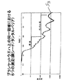
金属膜層と基板の間の界面で反射される放射は、干渉効果を示す反射曲線を生み出して、干渉するであろう。図2は、2つのそのような角度反射スペクトルを示す。上部スペクトル曲線S2は、基板上にタンタル層のものであり、底部スペクトル曲線S1は、基板上に銅のものである。この変動は、測定信号S1及びS2における干渉縞18の出現を起こす。反射率がそんなに小さい(典型的に、1より遙かに小さい)ので、多重反射は、X線反射信号において比較的検出できない効果を有する。両曲線では、Ψを増やすことで反射率は急激に減少する。
【0008】
実際には、X線の入射角は、X線源を移動し、あるいはサンプルを傾けることによって変化され得る。上述の先行技術では、多数のX線入射角は、線源放射を集束することによって作り出され得る。それは、異なる入射角でサンプルに衝突するために、ビーム内の光線を曲げるように機能する。
【0009】
線源とサンプルの間の角度を積極的に変更することを要求する従来のX線反射器あるいはXRR提案で用いられ得るけれども、主発明の概念は、同時に多数の入射角実施例、すなわち、高速X線反射計あるいは「RXRR」提案で最も好ましく用いられる。
【0010】
また、主発明は、X線エネルギーの広域スペクトルが固定角度で適用されるエネルギー分散方式技術に適用され得る。そのような広域スペクトルX線放射は、回転陽極の制動放射輻射によって適当に生成され得る。X線反射は、各エネルギーで計測される。そのようなエネルギー分散方式X線技術は、Chason他のPhys. Rev. Lett. 72, 3040(1994年)及びChason他のAppl. Phys. Lett. 60, 2353(1992年)に記述される。これらはそれぞれ全部参照にここに組み込まれる。
【0011】
金属層の測定は、半導体パターンウエハ上では非常に困難である。XRR又はRXRRの典型的な測定スポットサイズは1mm以上である。パターンウエハの形状が1ミクロンオーダーであり、パターンウエハ上のテストサイトでさえ100ミクロンより一般的に小さい寸法を有するので、パターンウエハ上の単一又は二層金属厚の正確な決定は、非常に困難であると信じられていた。
【0012】
ここに記述される提案は、パターンウエハ上の形状より大きい1mmスポットサイズをさらに用いて、パターンウエハ上の1、2又はそれ以上の層(不透明なあるいは誘電性の金属)厚を測定する可能性を提供する。
【0013】
発明の概要
主発明の教示は、XRR及びRXRRシステムの新しい応用を導く。特に、そのようなシステムが形状が測定スポットよりも小さいパターンかウエハ上の種々の薄膜(誘電性で、不透明な金属膜の両方)の厚さを測定するために用いられ得る。概して、本発明の一面は、XRR及びRXRRシステムがテストウエハ上のみならず、同様にパターンウエハ上においても用いられ得るという認識である。ここで特定の技術は、この基本概念を単純化し、拡張するのを助けるように意図される。しかしながら、この開示の前に、誰も小さい形状を持つパターンウエハにおいてそのようなシステムを用いようと試みたことを我々が知らないことを理解されたい。
【0014】
図5は、シリコン基板22、誘電体層24及び金属層26から成るパターンウエハ20を示す。図に示すように、金属層26の厚さは一定であるが、その下の酸化物層24は、X線ビーム30からスポットの径全体にわたって厚さが劇的に変化する。実際に量を定めることを困難にさせるこのような変化にかかわらず、金属層26の厚さがXRR又はRXRR技術を用いてさらに正確に決定され得ることが、見出された。
【0015】
数学的解析は、X線反射信号は、主として、金属層の上部表面と、金属層と酸化物層の境界との間の干渉による効果から来るので、このような結果が達成され得ることを示していた。非常に小さい信号となるのは、上述のように、酸化物層の厚さが際立って変化することによるものである。酸化物層からの信号があまりに小さいという理由の一部は、そのような比較的厚い層のために、どの縞もそれらが見られないほど互いに近いことであろう。加えて、上述のように、反射率があまりに小さいので、多重反射は、X線反射信号において相対的に検出できない程度の影響を及ぼす。上記を考慮すると、層の厚さの決定ができるようにしたまま、パターンウエハからの信号の数学的モデリングを、単純化することができる。
【0016】
好ましい実施の形態の詳細な記述
薄膜の所定のサンプルのために、X線反射は、X線波長(λ)、入射角、並びに、層を作る材料の厚さ及び光学的特性の関数であるフレネルの式モデリングを用いて決定され得る。典型的に、全反射が起こる臨界角は、非常に小さい(およそ0.1〜0.5°)。入射角が臨界角以上に増加されるにつれて、反射率が非常に急速に落ちるので、小さい角X線反射は、実験的に重要である。小さい角近似(sinΨ≒Ψ)の下で、層n−1と層nの間の界面におけるX線反射の再帰方程式は、以下のように与えられる:
【式1】

an=exp((−iπ/λ)fndn)である。
【0017】
ここで、dnは、層nの厚さであり、Ψc(n)は、層nの材料上に入射される波長λのX線のために全反射が起こる入射角である。
【0018】
fnは、fn=An−iBnによって与えられ、ここで、
【式2】
【0019】
これらの再帰方程式は、薄膜スタックの底から始めて、基板に対応する層n=NでRN,N+1を0に設定し、結果として生じる再帰方程式を実行することによって解く。真空に対応する層n=1で、その複素共役を持つR1,2の積|R1,2|2は、入射X線強度に対する反射X線強度の比で与えられる。
【0020】
界面の深さからの複雑化及び微視的表面粗さと同様に、伝統的なフルネルの式に基づくX線反射の理論モデリングは、次の参考文献、すなわち、L. G. ParrattのPhys. Rev. 95, 359 (1954年)、C.A. Lucas他のJ. Appl. Phys. 63, 1936 (1988年)、及びM. ToneyとS. BrennanのJ. Appl. Phys. 66, 1861(1989年)においてより詳細に記述される。これらはそれぞれ全部参照によりここに組み込まれる。
【0021】
XRRを用いてパターン半導体ウエハの膜厚を測定する一提案は、測定されたX線反射曲線がパターンの構造よりもむしろ層の厚さに主として帰され得るという認識に頼る。XRR測定に用いられるX線の波長は、数オングストロームのオーダーである。10,000オングストロームのオーダーであるパターンウエハの形状に比較して、その波長は非常に小さい。それゆえ、パターン自体の構造からの干渉効果は重要ではない。
【0022】
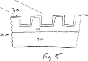
例えば、一つは、図5に示されるような垂直断面を有する一タイプの線形パターンのラインに垂直な入射平面を持つX線を考慮してもよい。干渉効果が比較的重要でないので、X線反射曲線の形状は、同じ層を有するパターン化されていない半導体ウエハのそれと比較して、パターンによって相対的に変化していない。最も顕著な効果は、凹部の側面及び底に入射する光の一部が反射信号にあまり貢献しないので、反射X線強度が一般に減少され得るということである。凹部の深さが測定される層の厚さに比べて大きいとき、全体的強度の減少以上にX線反射曲線における小さい変化のみが見られる。
【0023】
ここで用いられるように、「パターンウエハ」又は「パターン半導体ウエハ」は、X線プローブビームのスポットサイズよりも小さいサイズの人為的パターンをウエハの表面に有する半導体ウエハを意味する。上述のように、典型的に、プローブビームの測定スポットサイズは、1mm以上であるが、パターンの形状は、大きさで1ミクロンのオーダーであり、パターンウエハ上のテストサイトでさえ、100ミクロンより典型的に小さい直径を有する。従って、X線プローブビームスポットサイズとパターンウエハ上のテストサイトのサイズとを区分するものとして、通常は少なくとも一桁分のオーダーのサイズの差がある。
【0024】
パターンウエハのX線反射曲線の解析は、類似した層を有するパターン化されない(パターンのない)ウエハ上でなされる測定との比較を通して、大いに単純化され得る。パターンのない比較ウエハは、単に、パターンウエハ上のパターンのない領域であってもよく、このパターンのない領域はパターンウエハと同様の積層がなされている。図3は、タンタルの境界層の上部に銅の最外殻層を有するパターンのないウエハでなされる測定からのX線反射データのグラフを示す。そのグラフは、対数目盛で入射角の関数として反射率を示し、実際には、米国特許第5,691,548号に記述されるタイプのXRR装置を用いてなされた5つの測定実行から5つの重ね合わされた曲線を示す。
【0025】
図6は、銅及びタンタルの最外殻層を同じく有するパターンウエハ(実際には、図3を作るために測定した同じウエハ上のパターン領域)でなされた測定からのX線反射データのグラフを示す。そのグラフは、対数目盛で入射角の関数として反射率を示し、さらに、5つの測定実行から5つの重ね合わされた曲線を示す。
【0026】
図3及び図6の形状の類似性は顕著である。本発明によれば、パターンウエハの解析は、データの比較的単純な変換を通してパターンのないウエハを解析する問題に帰することができる。そのようなデータの変換を適用する結果は、以下の図表に要約される。
【0027】
パターン化されないウエハにおける5つの測定
及びパターンウエハにおける5つの測定
(PVD銅シード/タンタルバリアを持つ姉妹ウエハ)
【表1】
フルネルの式モデリングは、パターン化されないウエハの層厚を見出すために反射率データに適用された。そして、その結果は、上記表の右部分で報告される。必要なパラメータは、周知のMarquardt-Levenbergアルゴリズムのような反復非線形最小二乗最適化技術を通して見出されうる。この目的のための最適な反復最適化技術は、Fanton他の「ビームプロフィール反射計を用いる薄膜のマルチパラメータ測定」、応用物理学会誌第73巻第11号7035頁(1993年)及びLeng他の「分光測光法及びビームプロフィール反射計を用いる絶縁膜スタックにおけるシリコン6層の同時測定」、応用物理学会誌第81巻第8号3570頁(1997年)に記述される。これら2つの論文は、全部参照によってここに組み込まれる。
【0029】
パターンウエハデータの場合、パターンウエハ反射曲線RP(θ)とパターン化されないウエハ反射曲線RU(θ)の近い類似度に基づいて、単純な変換が適用される。(ここで、θは入射角であるが、波動ベクトル移動のような他の従属変数も用いられ得る。)変換関数T(θ)は、RP(θ)×T(θ)がRU(θ)に密接に近づくように選択される。RP(θ)とRU(θ)の類似は、T(θ)が適切にθの単純な線形関数にであり得るようである。しかしながら、例えば、T(θ)が適切にθの二次方程式又は三次関数、あるいは角スペクトルの異なる部分の関数のような「スプライシング」であり得るように、より複雑な関数も選択され得る。
【0030】
単純な線形変換関数T(θ)を用いて、パターンウエハのデータは変換された。その点で、パターン化されないウエハに適用された同じフルネルの式モデリングは、パターンウエハの層厚を見出すために、変換された反射率データに適用された。その結果は、上記表の左部分で報告される。必要なパラメータは、再び、周知のMarquardt-Levenbergアルゴリズムのような反復非線形最小二乗最適化技術を通して見出され得る。
【0031】
層厚が決定されると、R−Ψ曲線を解析することができ、密度と表面及び界面粗度の値を得ることができる。
【0032】
パターン化されないウエハの層厚を見出すもう一つの提案は、フーリエ変換解析を用いることである。フーリエ変換解析は、Seeck他のAppl. Phys. Lett. 76, 2713(2000年)においてポリマー系の層厚を見出すために適用された。それは全部参照によってここに組み込まれる。指数フーリエ変換は、入射角よりもむしろ従属変数として波動ベクトル移動qzを用いて適用される。ここで、qzは、反射光線波動ベクトルと入射光線波動ベクトルの間の差として定義される。特に、変換関数F(d)が用いられる。ここで、dは層厚を表し、F(d)は以下のように与えられる:
【式3】
そのようなフーリエ変換解析が適用されるとき、変換関数曲線のピークは、サンプルの電子密度が急速に変化する領域に対応する。換言すれば、変換関数のピークは、層界面間の距離を示す。フーリエ変換アプローチは、非常に有力であり、同様の積層を持つパターンのないウエハからのデータを参照することなく、パターンウエハからのデータに適用され得る。フーリエ変換技術は、O. Glatter及びO. Kratkyの「小さい角X線散乱」アカデミックプレス社(1982年)の126〜136頁において幾分詳細に記述される。これらの頁は、全部参照によってここに組み込まれる。
【0034】
もう一つの提案では、異なる縞形態がデータ中に認識できるとき、パターンウエハ上の金属膜の層厚は、次のような修正ブラッグの式との照合によって決定され得る:
sin2Ψi=sin2Ψc+(i+1/2)2(λ/2d)2
ここで、「Ψi」は縞最大がある角度であり、Ψcは臨界角であり、iは値1,2,3,・・・を持つ正の整数であり、λはX線は長であり、dは層厚である。
【0035】
Ψi及びΨcが非常に小さい角度であり、修正ブラッグの式がΨc=0を含むすべての臨界角で有効でなければならないので、この近似値では、隣接する界面縞間の角間隔は、所定の厚さdで一定であり、以下によって与えられる:
ΔΨ=λ/2d
【0036】
この提案を用いて、厚さd(ΔΨ)=λ/(2ΔΨ)は、曲線の各縞間隔に結び付けられ得る。入射角が増加するにつれて近似ブラッグ式がより確かになるので、漸近解析は、増加するθの関数としてd(ΔΨ)をプロットし、漸近線を推定することによって、真の厚さdを見出すために適用され得る。
【0037】
所定の層(又は多層)からの干渉縞が認識できることを保証するために、多くの方法が用いられ得る。これらの方法は以下のものを含む。
【0038】
a.所定の層(又は多層)の干渉縞を最大にするための適切なX線波長の使用。例えば、タングステン源からのX線は、銅及びタンタル薄膜層でうまく機能することが分かった。選択されるX線波長は、すべての界面からの反射が外部的に観察される信号において効果を有するように、試験中多層構造を通して完全に貫通する。しばしば、その放射がキー多層構成の吸収端の低エネルギー(高透過)の側であるように、X線管ターゲット要素が選択される。好ましくは、多層構成及び選択されたX線波長は、種々の多層構成の反射スペクトルへの貢献の間の高レベルの対比があるようにである。
銅及びタングステンX線の両方が特にうまく銅及びタンタル薄膜を貫通し、半導体産業で用いられるタンタル上の銅(又は窒化タンタル)構造を計測するための候補波長を表す。これらについて、タングステン、すなわち、耐火金属は、X線管ターゲットとして用いられるとき一層信頼性が高く、長く続いて、適用のために選ばれた。
【0039】
b.必要ならば、所定のフルの厚さ範囲を覆い、あるいは、1層以上からより容易に縞を識別するための1以上のX線波長の使用。
【0040】
c.縞対比を最大にするようにパターン特性に関してすれすれのX線ビームの適切な方向でウエハを放射線処理する。例えば、線パターンの場合、ビームは、入射面が線パターンのラインに平行であるように、方向付けられ得る。
【0041】
d.基礎を為す層からの競合縞信号を最小にするための適切なX線波長の使用。
【0042】
基本的な例では、タンタルの薄いバリア層の上部に銅からなる層スタックを想定する。我々が適切なX線波長λを注意深く選ぶならば、銅の単層(S1)及びタンタルの単層(S2)のためのR−Ψ曲線(図2に示される)を得るかもしれない。タンタルが銅より密であるので、その曲線S2の縞は、より高いΨ値である。同じく、タンタル層が銅層より薄いので、タンタル曲線S2の干渉縞は、更に離れて離隔される。
【0043】
図3は、タンタル層が銅層の下に見出されるときを測定するR−Ψ曲線S3を表す。(図4はこの層構造を示す。)図3に見られるように、より低いΨ領域では銅の縞だけあるが、より高いΨ領域ではタンタル縞が銅縞よりかなり強いので、銅及びタンタルの両方の干渉縞が、個々に認識できる。
【0044】
上述のように、銅及びタンタル縞の両方間の間隔は、基礎を為す層あるいは粗度に強く依存しない。従って、銅及びタンタルの両層の厚さは、パターンウエハ上でさえ縞間隔から明白に決定され得る。この方法を用いて決定された層厚は、1mmの測定領域にわたっての平均厚さであろう。しかしながら、沈積層の厚さが典型的に1mmの寸法にわたってあまり変化しないので、この測定平均は妥当である。また、パターンウエハ上に存在するわずかなトポグラフィ(地形)が厚さ測定に顕著に影響を与えないことに気付かれたい。
【0045】
正しいX線波長の選択は、2層の構成及び評価するのに必要な厚さ範囲に依存する。理想的には、一つの波長は、両層の要求される厚さ範囲における所定の2層からの干渉縞の明白な測定を可能にする。
【0046】
しかしながら、それは、上記基準を満たす一つの波長を見出すことができないということかもしれない。その場合、2つのX線波長は、スタックにおける一つの層上の良い縞データを提供する一つの波長と、スタックにおける他の層上の良い縞データを提供する他方で用いられ得る。両データセットを用いて、両層の厚さが決定され得る。実際には、縞間の間隔を解析するとき、測定縞分離と予測縞分離とを比較するために、従来の最小二乗法ルーチンを用い得る。
【0047】
2つのX線波長を作り出すために、2つのX線源を用いる必要があるかもしれない。これらの2つの線源は、タレット(例えば)上にその線源を据え付け、ウエハの同一領域について一連の測定のために同位置に各線源を導くことによって、連続的に用いられ得る。その代わりに、離れた90°の位置で2つの線源を据え付け、同一領域上に両放射ビーム焦点を同時に持つことができる。
【0048】
必要ならば、例えば、2以上の層を含む層スタック上の金属層を扱うとき、この概念は、2以上のX線源に拡張され得る。同様に、2以上の個々の線源の代わりに多線X線源を用いることもできる。多線X線源は、2以上の要素から成るX線ターゲットを用いることによって作られてもよい。また、シンクロトロン又は加速装置のような連続的なX線源を用いることもできる。
【0049】
上述の同一の概念は、誘電性で透過するあるいは部分的に吸収する薄膜に同等の有効性で適用され得る。そのような薄膜は、分光測定法、反射計及び偏向解析法のような従来の光学的方法で測定され得るけれども、XRR又はRXRRがより効果的であり得る場合もある。これらの場合は、光学的パラメータが知られず、あるいは正確に決定できないときでさえ、膜厚が計算される必要がある状況を含む。これは、部類分けされた光学的パラメータや空間的に変化するパラメータを持つ薄膜を持つ場合である。
【0050】
本発明の範囲は、次の特許請求の範囲に示されるもの及びその同等物であると意図され、上述のあらゆる特定の実施の形態に限定されない。
【図面の簡単な説明】
【図1】 好ましいX線反射計システムを示す。
【図2】 2つの異なるサンプル、すなわち、銅層を持つ一つとタンタル層を持つ一つからの反射データのための、サンプルへの入射角の関数であるサンプルX線反射の正規化グラフを示す。
【図3】 銅とタンタルの両層を持つパターン化されないサンプルからの反射データのための、サンプルへの入射角の関数であるサンプルX線反射のグラフを示す。
【図4】 半導体基板上に銅層とタンタル層を持つサンプルの単純化された断面図及び三層の界面からのX線の反射を示す。
【図5】 パターンウエハサンプル上の境界の線パターンの断面図及びサンプルの表面へのX線の入射を示す。
【図6】 パターンウエハサンプルからの反射データのための、サンプルへの入射角の関数であるサンプルX線反射のグラフを示す。[0001]
This application claims the benefit of US Provisional Patent Application Nos. 60 / 162,679 and 60 / 146,832. These provisional patent applications were filed on November 1, 1999 and August 2, 1999, both of which are incorporated herein by reference.
[0002]
BACKGROUND OF THE INVENTION The semiconductor industry is continuously interested in measuring thin films formed on wafers. Many metrology devices have been developed for these measurements. Many of these devices rely on probing the sample with a radiation beam having a wavelength in the visible and / or ultraviolet region. These devices work very well with many different types of films that are at least partially transparent at these wavelengths. Unfortunately, these devices are not effective for investigating opaque metal films because opaque metal films (such as copper) do not transmit ultraviolet or visible radiation.
[0003]
In recent years, several techniques using wavelengths in X-ray therapy have been developed. These X-ray reflectivity techniques (XRR) have several advantages over techniques that use visible light. One such advantage is the ability to measure the thickness of ultra-thin films on the order of XRR of 30 angstroms or less. Visible light is not suitable for investigating such ultra-thin films using interference fringes because of its wavelength. However, the XRR system may rather use radiation at a wavelength of approximately 1.5 angstroms. The radiation creates the appropriate fringes even when examining such ultra-thin films. In addition, XRR can be suitably used where the film is composed of a light opaque material such as a metal or metal compound. Another possible application of the XRR method is as an in-situ monitor where only the glazing angle of the radiation beam can be used to monitor a sample in the process chamber. Finally, XRR is used accordingly to measure the density and thickness of films made of materials with a low dielectric constant and a low refractive index, such as certain polymers, fluorocarbon compounds, and aerogels. Can be.
[0004]
A preferred XRR technique is described in US Pat. No. 5,619,548, issued April 8, 1997, incorporated herein by reference. FIG. 1 illustrates this preferred technique. (See also Japanese Patent No. 2,720,131 issued on November 21, 1997)
[0005]
In FIG. 1, the preferred X-ray scattering system includes an X-ray source 31 that produces an
[0006]
In the basic system, the probe beam of x-ray radiation is directed to impinge on the sample at an angle selected so that it is at least partially reflected. The sample may typically consist of a substrate coated with one or more thin metal layers. All x-ray radiation will be reflected at a very shallow angle below the critical angle (Ψ c ) (as measured between the surface of the sample and the incident beam). As the angle of incidence of the incident beam increases with respect to the sample surface, the incident amount of radiation will propagate through the upper metal layer and the amount of reflected light will decrease. Some radiation propagating through the metal layer will reach the interface between the metal film and the substrate and will be reflected back to the substrate.
[0007]
Radiation reflected at the interface between the metal film layer and the substrate will interfere, creating a reflection curve that exhibits interference effects. FIG. 2 shows two such angular reflection spectra. Upper spectrum curve S 2 is of the tantalum layer on a substrate, the bottom spectrum curve S 1 are those of copper on the substrate. This variation causes the appearance of interference fringes 18 in the measurement signals S 1 and S 2 . Since the reflectivity is so small (typically much less than 1), multiple reflection has a relatively undetectable effect in the X-ray reflected signal. In both curves, the reflectance decreases rapidly as Ψ increases.
[0008]
In practice, the angle of incidence of X-rays can be changed by moving the X-ray source or tilting the sample. In the prior art described above, multiple X-ray incident angles can be created by focusing the source radiation. It functions to bend the rays in the beam to strike the sample at different angles of incidence.
[0009]
Although it can be used in conventional X-ray reflectors or XRR proposals that require aggressively changing the angle between the source and the sample, the concept of the main invention is that multiple incident angle embodiments, i.e., fast Most preferably used in the X-ray reflectometer or “RXRR” proposal.
[0010]
The main invention can also be applied to an energy dispersion technique in which a wide spectrum of X-ray energy is applied at a fixed angle. Such broad spectrum X-ray radiation can be suitably generated by bremsstrahlung radiation of the rotating anode. X-ray reflection is measured at each energy. Such energy dispersive X-ray techniques are described in Chason et al. Phys. Rev. Lett. 72, 3040 (1994) and Chason et al. Appl. Phys. Lett. 60, 2353 (1992). Each of which is incorporated herein by reference in its entirety.
[0011]
Measurement of the metal layer is very difficult on a semiconductor pattern wafer. A typical measurement spot size of XRR or RXRR is 1 mm or more. Since the shape of the pattern wafer is on the order of 1 micron and even test sites on the pattern wafer have dimensions generally smaller than 100 microns, an accurate determination of single or double layer metal thickness on the pattern wafer is very It was believed to be difficult.
[0012]
The proposal described here has the potential to measure the thickness of one, two or more layers (opaque or dielectric metal) on the patterned wafer, further using a 1 mm spot size larger than the shape on the patterned wafer. I will provide a.
[0013]
SUMMARY OF THE INVENTION The teachings of the main invention lead to new applications of XRR and RXRR systems. In particular, such a system can be used to measure the thickness of various patterns (both dielectric and opaque metal films) on the wafer or a pattern whose shape is smaller than the measurement spot. In general, one aspect of the present invention is the recognition that XRR and RXRR systems can be used not only on test wafers, but also on patterned wafers. Here, certain techniques are intended to help simplify and extend this basic concept. However, it should be understood that prior to this disclosure we do not know that anyone has attempted to use such a system on a patterned wafer with a small shape.
[0014]
FIG. 5 shows a patterned
[0015]
Mathematical analysis indicates that such a result can be achieved because the X-ray reflected signal mainly comes from the effect of interference between the upper surface of the metal layer and the boundary between the metal layer and the oxide layer. It was. Become very small signals, as described above, it is by changing markedly the thickness of the oxide layer. Part of the reason that the signal from the oxide layer is so small would be that due to such a relatively thick layer, any stripes are so close together that they are not seen. In addition, as described above, the reflectivity is so small that multiple reflections have a relatively undetectable effect on the X-ray reflected signal. In view of the above, mathematical modeling of the signal from the patterned wafer can be simplified while allowing the thickness of the layer to be determined .
[0016]
Detailed Description of Preferred Embodiments For a given sample of thin film, X-ray reflection is a function of X-ray wavelength (λ), angle of incidence, and the thickness and optical properties of the material from which the layer is made. Can be determined using formula modeling. Typically, the critical angle at which total reflection occurs is very small (approximately 0.1-0.5 °). Small angular X-ray reflection is experimentally important because the reflectivity drops very rapidly as the incident angle is increased beyond the critical angle. Under a small angular approximation (sin Ψ≈Ψ), the recurrence equation for X-ray reflection at the interface between layer n-1 and layer n is given as:
[Formula 1]
a n = exp ((− iπ / λ) f n d n ).
[0017]
Here, d n is the thickness of the layer n, Ψ c (n) is the angle of incidence total reflection occurs for the X-ray wavelength λ incident on the material of the layer n.
[0018]
f n is given by f n = A n −iB n , where
[Formula 2]
[0019]
These recurrence equations are solved by starting from the bottom of the thin film stack and setting RN, N + 1 to 0 in the layer n = N corresponding to the substrate and executing the resulting recurrence equation . A layer n = 1 corresponding to the vacuum, the product of R 1, 2 with the
[0020]
Similar to the complexity from the depth of the interface and the microscopic surface roughness, the theoretical modeling of X-ray reflection based on the traditional Frunnel equation can be found in the following reference: LG Parratt Phys. Rev. 95, 359 (1954), CA Lucas et al., J. Appl. Phys. 63, 1936 (1988), and M. Toney and S. Brennan, J. Appl. Phys. 66, 1861 (1989). Described. Each of which is incorporated herein by reference in its entirety.
[0021]
One proposal for measuring the thickness of a patterned semiconductor wafer using XRR relies on the recognition that the measured X-ray reflection curve can be attributed primarily to the layer thickness rather than the pattern structure. The wavelength of X-rays used for XRR measurement is on the order of several angstroms. Compared to the shape of a patterned wafer on the order of 10,000 angstroms, its wavelength is very small. Therefore, the interference effect from the structure of the pattern itself is not important.
[0022]
For example, one may consider X-rays having an incident plane perpendicular to a line of one type of linear pattern having a vertical cross-section as shown in FIG. Since the interference effect is relatively unimportant, the shape of the X-ray reflection curve is relatively unchanged from pattern to pattern compared to that of an unpatterned semiconductor wafer having the same layer. The most striking effect is that the reflected X-ray intensity can generally be reduced because some of the light incident on the sides and bottom of the recess does not contribute much to the reflected signal. When the depth of the recess is large compared to the thickness of the layer being measured, only a small change in the X-ray reflection curve is seen beyond the overall intensity decrease.
[0023]
As used herein, “pattern wafer” or “pattern semiconductor wafer” means a semiconductor wafer having an artificial pattern on the surface of the wafer that is smaller than the spot size of the X-ray probe beam. As described above, the measurement spot size of the probe beam is typically 1 mm or more, but the shape of the pattern is on the order of 1 micron in size, and even at a test site on the pattern wafer, more than 100 microns. Typically has a small diameter. Accordingly, there is usually a difference in size of at least an order of magnitude as a part for distinguishing the X-ray probe beam spot size from the size of the test site on the pattern wafer .
[0024]
Analysis of the X-ray reflection curve of a patterned wafer can be greatly simplified through comparison with measurements made on unpatterned (unpatterned) wafers with similar layers. The comparison wafer without a pattern may simply be an area without a pattern on the pattern wafer, and the area without the pattern is laminated in the same manner as the pattern wafer . Figure 3 shows a graph of X-ray reflection data from measurements made in a wafer without a pattern on top of the boundary layer of tantalum having outermost layer of copper. The graph shows reflectivity as a function of angle of incidence on a logarithmic scale, and in fact, from five measurement runs made using an XRR instrument of the type described in US Pat. No. 5,691,548. A superimposed curve is shown.
[0025]
FIG. 6 shows a graph of X-ray reflection data from measurements made on a patterned wafer (actually, a pattern area on the same wafer measured to make FIG. 3) that also has an outermost layer of copper and tantalum . Show. The graph shows reflectivity as a function of incident angle on a logarithmic scale, and further shows five superimposed curves from five measurement runs.
[0026]
The similarity of the shapes of FIGS. 3 and 6 is remarkable. According to the present invention, the analysis of a patterned wafer can be attributed to the problem of analyzing a wafer without a pattern through a relatively simple transformation of data. The results of applying such data transformations are summarized in the following chart.
[0027]
5 measurements on unpatterned wafer and 5 measurements on patterned wafer (Sister wafer with PVD copper seed / tantalum barrier)
[Table 1]
Fullel's formula modeling was applied to the reflectance data to find the unpatterned wafer layer thickness. The results are reported in the right part of the above table. The necessary parameters can be found through iterative nonlinear least squares optimization techniques such as the well-known Marquardt-Levenberg algorithm. Optimal iterative optimization techniques for this purpose are described in Fanton et al., “Multiparameter Measurement of Thin Films Using Beam Profile Reflectometers,” Journal of Applied Physics, Vol. 73, No. 11, page 7035 (1993) and Leng et al. "Simultaneous measurement of six silicon layers in an insulating film stack using spectrophotometry and a beam profile reflectometer", Journal of Applied Physics, Vol. 81, No. 8, page 3570 (1997). These two articles are hereby incorporated by reference in their entirety.
[0029]
In the case of pattern wafer data, a simple transformation is applied based on the close similarity between the pattern wafer reflection curve RP (θ) and the unpatterned wafer reflection curve RU (θ). (Here, θ is the angle of incidence, but other dependent variables such as wave vector movement can also be used.) For the transformation function T (θ), RP (θ) × T (θ) is RU (θ). Selected to approach closely. The resemblance between RP (θ) and RU (θ) seems to be that T (θ) can be suitably a simple linear function of θ. However, more complex functions can also be selected so that, for example, T (θ) can be “splicing”, such as a quadratic or cubic function of θ, or a function of a different part of the angular spectrum.
[0030]
The pattern wafer data was transformed using a simple linear transformation function T (θ). In that regard, the same full-nel formula modeling applied to the unpatterned wafer was applied to the transformed reflectance data to find the layer thickness of the patterned wafer. The results are reported in the left part of the table above. The necessary parameters can again be found through iterative nonlinear least squares optimization techniques such as the well-known Marquardt-Levenberg algorithm.
[0031]
Once the layer thickness is determined, the R-Ψ curve can be analyzed and values for density and surface and interface roughness can be obtained.
[0032]
Another proposal for finding the layer thickness of the unpatterned wafer is to use Fourier transform analysis. Fourier transform analysis was applied to find the layer thickness of polymer systems in Seeck et al. Appl. Phys. Lett. 76, 2713 (2000). It is incorporated herein by reference in its entirety. Exponential Fourier transform is applied using the wavevector movement q z rather as a dependent variable than the incident angle. Here, q z is defined as the difference between the reflected ray wave vector and the incident ray wave vector. In particular, the conversion function F (d) is used. Where d represents the layer thickness and F (d) is given as:
[Formula 3]
When such a Fourier transform analysis is applied, the peak of the transform function curve corresponds to a region where the electron density of the sample changes rapidly. In other words, the peak of the conversion function indicates the distance between the layer interfaces. The Fourier transform approach is very powerful and can be applied to data from patterned wafers without reference to data from unpatterned wafers with similar stacking . The Fourier transform technique is described in some detail in O. Glatter and O. Kratky, “Small Angle X-Ray Scattering”, Academic Press, pp. 126-136. These pages are hereby incorporated by reference in their entirety.
[0034]
In another proposal, when different fringe shapes can be recognized in the data, the layer thickness of the metal film on the patterned wafer can be determined by matching with the modified Bragg equation as follows:
sin 2 Ψ i = sin 2 Ψ c + (i + 1/2) 2 (λ / 2d) 2
Where “Ψ i ” is the angle at which the fringe maximum is, Ψ c is the critical angle, i is a positive integer with the
[0035]
Since Ψ i and Ψ c are very small angles and the modified Bragg equation must be valid for all critical angles including Ψ c = 0, in this approximation, the angular spacing between adjacent interface fringes is , Constant at a given thickness d, given by:
ΔΨ = λ / 2d
[0036]
With this proposal, the thickness d (ΔΨ) = λ / (2ΔΨ) can be tied to each fringe spacing of the curve. Since the approximate Bragg equation becomes more certain as the angle of incidence increases, the asymptotic analysis plots d (ΔΨ) as a function of increasing θ and finds the true thickness d by estimating the asymptote. Can be applied to.
[0037]
Many methods can be used to ensure that interference fringes from a given layer (or multiple layers) can be recognized. These methods include the following.
[0038]
a. Use an appropriate X-ray wavelength to maximize the interference fringes of a given layer (or multiple layers). For example, X-rays from a tungsten source have been found to work well with copper and tantalum thin film layers. The selected X-ray wavelength penetrates completely through the multilayer structure during the test so that reflections from all interfaces have an effect on the signal observed externally. Often, the X-ray tube target element is selected so that its radiation is on the low energy (high transmission) side of the absorption edge of the key multilayer configuration. Preferably, the multilayer configuration and the selected x-ray wavelength are such that there is a high level of contrast between the contribution of the various multilayer configurations to the reflection spectrum.
Both copper and tungsten x-rays penetrate the copper and tantalum thin films particularly well and represent candidate wavelengths for measuring copper (or tantalum nitride) structures on tantalum used in the semiconductor industry. For these, tungsten, a refractory metal, was more reliable when used as an X-ray tube target, and has been chosen for long-lasting applications.
[0039]
b. If necessary, use one or more x-ray wavelengths to cover a given full thickness range or more easily identify stripes from more than one layer.
[0040]
c. The wafer is radiation treated with the appropriate direction of the grazing X-ray beam with respect to the pattern characteristics to maximize the fringe contrast. For example, in the case of a line pattern, the beam can be directed so that the entrance surface is parallel to the lines of the line pattern.
[0041]
d. Use appropriate x-ray wavelengths to minimize competing fringe signals from the underlying layer.
[0042]
The basic example assumes a layer stack of copper on top of a thin tantalum barrier layer. If we carefully choose an appropriate X-ray wavelength λ, we may obtain R-Ψ curves (shown in FIG. 2) for a copper monolayer (S1) and a tantalum monolayer (S2). Since tantalum is denser than copper, the fringes on the curve S2 have higher Ψ values. Similarly, since the tantalum layer is thinner than the copper layer, the interference fringes of the tantalum curve S2 are further spaced apart.
[0043]
FIG. 3 represents an R-Ψ curve S3 that measures when a tantalum layer is found under the copper layer. (Figure 4 shows the layer structure.) As seen in FIG. 3, there is only stripes of copper at lower Ψ area, but because at higher Ψ region tantalum stripes considerably stronger than Doshima, copper and tantalum Both interference fringes can be recognized individually.
[0044]
As mentioned above, the spacing between both copper and tantalum stripes is not strongly dependent on the underlying layer or roughness. Thus, the thickness of both the copper and tantalum layers can be clearly determined from the stripe spacing even on the patterned wafer. The layer thickness determined using this method will be the average thickness over a measurement area of 1 mm. However, this measured average is reasonable because the thickness of the deposit is typically not very variable over the 1 mm dimension. It should also be noted that the slight topography present on the pattern wafer does not significantly affect the thickness measurement.
[0045]
The selection of the correct x-ray wavelength depends on the construction of the two layers and the thickness range required for evaluation. Ideally, one wavelength allows unambiguous measurement of interference fringes from a given two layers in the required thickness range of both layers.
[0046]
However, it may be that one wavelength that meets the above criteria cannot be found. In that case, two x-ray wavelengths can be used on one wavelength that provides good fringe data on one layer in the stack and on the other that provides good fringe data on the other layers in the stack. Using both data sets, the thickness of both layers can be determined. In practice, when analyzing the spacing between fringes, a conventional least squares routine can be used to compare the measured fringe separation with the predicted fringe separation.
[0047]
In order to create two x-ray wavelengths, it may be necessary to use two x-ray sources. These two sources can be used sequentially by mounting the source on a turret (for example) and directing each source to the same location for a series of measurements on the same area of the wafer. Alternatively, two sources can be installed at 90 ° apart and have both radiation beam focal points simultaneously on the same area.
[0048]
If necessary, this concept can be extended to more than one X-ray source, for example when dealing with metal layers on a layer stack containing more than one layer. Similarly, multi-ray X-ray sources can be used in place of two or more individual sources. A multi-ray X-ray source may be made by using an X-ray target consisting of two or more elements. A continuous X-ray source such as a synchrotron or an accelerator can also be used.
[0049]
The same concept described above can be applied with equal effectiveness to thin films that are dielectrically transmissive or partially absorbing. Such thin films can be measured by conventional optical methods such as spectroscopic methods, reflectometers and deflection analysis methods, although XRR or RXRR may be more effective. These cases include situations where the film thickness needs to be calculated even when the optical parameters are not known or cannot be accurately determined. This is the case with thin films with classified optical parameters and spatially varying parameters.
[0050]
The scope of the present invention is intended to be that shown in the following claims and their equivalents, and is not limited to any particular embodiment described above.
[Brief description of the drawings]
FIG. 1 shows a preferred X-ray reflectometer system.
FIG. 2 shows a normalized graph of sample x-ray reflection as a function of angle of incidence on a sample for reflection data from two different samples, one with a copper layer and one with a tantalum layer. .
FIG. 3 shows a graph of sample x-ray reflection as a function of angle of incidence on a sample for reflection data from an unpatterned sample having both copper and tantalum layers.
FIG. 4 shows a simplified cross-sectional view of a sample having a copper layer and a tantalum layer on a semiconductor substrate and reflection of X-rays from a three-layer interface.
FIG. 5 shows a cross-sectional view of a boundary line pattern on a patterned wafer sample and the incidence of X-rays on the surface of the sample.
FIG. 6 shows a graph of sample x-ray reflection as a function of angle of incidence on a sample for reflection data from a patterned wafer sample.
Claims (31)
X線のプローブビームを生成するステップと、
前記プローブビームのスポットサイズが前記パターン半導体ウエハの表面上のパターンの形状の大きさに比べて大きくなるように、前記パターン半導体ウエハの表面上に前記プローブビームを導くステップと、
反射データを生成するために、前記パターン半導体ウエハから反射される種々のX線の強度を測定するステップと、
前記薄膜層の特性を決定するために、前記反射データを解析するステップと、
を有することを特徴とする方法。A method for evaluating characteristics of a thin film layer of a patterned semiconductor wafer,
Generating an X-ray probe beam;
Directing the probe beam onto the surface of the patterned semiconductor wafer such that the spot size of the probe beam is larger than the size of the pattern shape on the surface of the patterned semiconductor wafer;
Measuring the intensity of various X-rays reflected from the patterned semiconductor wafer to generate reflection data;
Analyzing the reflection data to determine characteristics of the thin film layer;
A method characterized by comprising:
X線のプローブビームを生成するステップと、
集束されたプローブビーム内の種々のX線が前記パターン半導体ウエハ表面に関する入射角の範囲を作り、前記プローブビームのスポットサイズが前記パターン半導体ウエハの前記表面上のパターンの形状の大きさに比べて大きくなるように、前記パターン半導体ウエハの表面上に前記プローブビームを集束するステップと、
前記表面に関して特定の入射角に対応する反射されたプローブビーム内のX線の位置で反射されるプローブビーム内の位置の関数として、種々のX線の強度を測定するステップと、
前記薄膜層の特性を決定するために、前記反射データを解析するステップと、
を有することを特徴とする方法。A method for evaluating characteristics of a thin film layer of a patterned semiconductor wafer,
Generating an X-ray probe beam;
Various X-rays in the focused probe beam create a range of incident angles with respect to the surface of the patterned semiconductor wafer, and the spot size of the probe beam is compared to the size of the pattern on the surface of the patterned semiconductor wafer. Focusing the probe beam on the surface of the patterned semiconductor wafer to be large;
Measuring the intensity of various x-rays as a function of the position in the probe beam reflected at the position of the x-ray in the reflected probe beam corresponding to a particular angle of incidence with respect to the surface;
Analyzing the reflection data to determine characteristics of the thin film layer;
A method characterized by comprising:
エネルギーの広域スペクトルを有するX線のプローブビームを生成するステップと、
前記プローブビームのスポットサイズが前記パターン半導体ウエハの表面上のパターンの形状の大きさに比べて大きくなるように、前記パターン半導体ウエハの表面上に前記プローブビームを導くステップと、
X線エネルギーの関数として反射X線強度を測定する反射データを生成するために、前記パターン半導体ウエハから反射される種々のX線の強度を測定するステップと、
前記薄膜層の特性を決定するために、前記反射データを解析するステップと、を有することを特徴とする方法。A method for evaluating characteristics of a thin film layer of a patterned semiconductor wafer,
Generating an X-ray probe beam having a broad spectrum of energy;
Directing the probe beam onto the surface of the patterned semiconductor wafer such that the spot size of the probe beam is larger than the size of the pattern shape on the surface of the patterned semiconductor wafer;
Measuring the intensity of various X-rays reflected from the patterned semiconductor wafer to generate reflection data that measures reflected X-ray intensity as a function of X-ray energy;
Analyzing the reflection data to determine characteristics of the thin film layer.
X線のプローブビームを生成する線源と、
前記プローブビームのスポットサイズが前記パターン半導体ウエハの前記表面上のパターンの形状の大きさに比べて大きくなるように、前記パターン半導体ウエハの表面上に前記プローブビームを導く手段と、
反射データを生成するために、前記パターン半導体ウエハから反射される種々のX線の強度を測定する検出器と、
前記薄膜層の特性を決定するために、前記反射データを解析するプロセッサ手段と、
を備えることを特徴とする装置。An apparatus for evaluating characteristics of a thin film layer of a patterned semiconductor wafer,
A source for generating an X-ray probe beam;
Wherein as the spot size of the probe beam is greater than the size of the shape of the pattern on the surface of the pattern semiconductor wafer, and means for guiding the probe beam on the surface of the pattern semiconductor wafer,
A detector for measuring the intensity of various X-rays reflected from the patterned semiconductor wafer to generate reflection data;
Processor means for analyzing the reflection data to determine characteristics of the thin film layer;
A device comprising:
Applications Claiming Priority (7)
| Application Number | Priority Date | Filing Date | Title |
|---|---|---|---|
| US14683299P | 1999-08-02 | 1999-08-02 | |
| US60/146,832 | 1999-08-02 | ||
| US16267999P | 1999-11-01 | 1999-11-01 | |
| US60/162,679 | 1999-11-01 | ||
| US09/629,407 US6754305B1 (en) | 1999-08-02 | 2000-08-01 | Measurement of thin films and barrier layers on patterned wafers with X-ray reflectometry |
| US09/629,407 | 2000-08-01 | ||
| PCT/US2000/020988 WO2001009566A1 (en) | 1999-08-02 | 2000-08-02 | X-ray reflectometry measurements on patterned wafers |
Publications (3)
| Publication Number | Publication Date |
|---|---|
| JP2003529047A JP2003529047A (en) | 2003-09-30 |
| JP2003529047A5 JP2003529047A5 (en) | 2010-12-09 |
| JP4824888B2 true JP4824888B2 (en) | 2011-11-30 |
Family
ID=27386468
Family Applications (1)
| Application Number | Title | Priority Date | Filing Date |
|---|---|---|---|
| JP2001513799A Expired - Fee Related JP4824888B2 (en) | 1999-08-02 | 2000-08-02 | X-ray reflectivity measurement on patterned wafer |
Country Status (4)
| Country | Link |
|---|---|
| US (1) | US6754305B1 (en) |
| EP (1) | EP1203200A1 (en) |
| JP (1) | JP4824888B2 (en) |
| WO (1) | WO2001009566A1 (en) |
Families Citing this family (51)
| Publication number | Priority date | Publication date | Assignee | Title |
|---|---|---|---|---|
| US6408048B2 (en) | 2000-03-14 | 2002-06-18 | Therma-Wave, Inc. | Apparatus for analyzing samples using combined thermal wave and X-ray reflectance measurements |
| JP2003532306A (en) | 2000-05-04 | 2003-10-28 | ケーエルエー・テンコール・テクノロジーズ・コーポレーション | Method and system for lithographic process control |
| GB0014587D0 (en) * | 2000-06-14 | 2000-08-09 | Europ Economic Community | X-ray reflectivity apparatus and method |
| US7062013B2 (en) * | 2001-04-12 | 2006-06-13 | Jordan Valley Applied Radiation Ltd. | X-ray reflectometry of thin film layers with enhanced accuracy |
| US7379175B1 (en) | 2002-10-15 | 2008-05-27 | Kla-Tencor Technologies Corp. | Methods and systems for reticle inspection and defect review using aerial imaging |
| US7027143B1 (en) | 2002-10-15 | 2006-04-11 | Kla-Tencor Technologies Corp. | Methods and systems for inspecting reticles using aerial imaging at off-stepper wavelengths |
| US7123356B1 (en) | 2002-10-15 | 2006-10-17 | Kla-Tencor Technologies Corp. | Methods and systems for inspecting reticles using aerial imaging and die-to-database detection |
| US7120228B2 (en) * | 2004-09-21 | 2006-10-10 | Jordan Valley Applied Radiation Ltd. | Combined X-ray reflectometer and diffractometer |
| JP3912606B2 (en) | 2004-10-26 | 2007-05-09 | 株式会社リガク | X-ray thin film inspection apparatus, thin film inspection apparatus for product wafer and method thereof |
| US7110491B2 (en) * | 2004-12-22 | 2006-09-19 | Jordan Valley Applied Radiation Ltd. | Measurement of critical dimensions using X-ray diffraction in reflection mode |
| US7804934B2 (en) | 2004-12-22 | 2010-09-28 | Jordan Valley Semiconductors Ltd. | Accurate measurement of layer dimensions using XRF |
| US7103142B1 (en) * | 2005-02-24 | 2006-09-05 | Jordan Valley Applied Radiation Ltd. | Material analysis using multiple X-ray reflectometry models |
| US7113566B1 (en) | 2005-07-15 | 2006-09-26 | Jordan Valley Applied Radiation Ltd. | Enhancing resolution of X-ray measurements by sample motion |
| US7570796B2 (en) | 2005-11-18 | 2009-08-04 | Kla-Tencor Technologies Corp. | Methods and systems for utilizing design data in combination with inspection data |
| KR101374308B1 (en) * | 2005-12-23 | 2014-03-14 | 조르단 밸리 세미컨덕터즈 리미티드 | Accurate measurement of layer dimensions using xrf |
| US7481579B2 (en) * | 2006-03-27 | 2009-01-27 | Jordan Valley Applied Radiation Ltd. | Overlay metrology using X-rays |
| US20070274447A1 (en) * | 2006-05-15 | 2007-11-29 | Isaac Mazor | Automated selection of X-ray reflectometry measurement locations |
| DE102006030874B4 (en) * | 2006-07-04 | 2013-03-14 | Pro-Beam Ag & Co. Kgaa | Method and device for machining workpieces |
| IL180482A0 (en) * | 2007-01-01 | 2007-06-03 | Jordan Valley Semiconductors | Inspection of small features using x - ray fluorescence |
| JP4977498B2 (en) * | 2007-03-09 | 2012-07-18 | 株式会社日立製作所 | Thin film laminate inspection method |
| US7680243B2 (en) * | 2007-09-06 | 2010-03-16 | Jordan Valley Semiconductors Ltd. | X-ray measurement of properties of nano-particles |
| KR101841897B1 (en) | 2008-07-28 | 2018-03-23 | 케이엘에이-텐코어 코오포레이션 | Computer-implemented methods, computer-readable media, and systems for classifying defects detected in a memory device area on a wafer |
| US8243878B2 (en) * | 2010-01-07 | 2012-08-14 | Jordan Valley Semiconductors Ltd. | High-resolution X-ray diffraction measurement with enhanced sensitivity |
| US8687766B2 (en) | 2010-07-13 | 2014-04-01 | Jordan Valley Semiconductors Ltd. | Enhancing accuracy of fast high-resolution X-ray diffractometry |
| EP3035047B1 (en) | 2010-11-12 | 2019-03-20 | EV Group E. Thallner GmbH | Measuring device and method for measuring layer thicknesses and defects in a wafer stack |
| US8437450B2 (en) | 2010-12-02 | 2013-05-07 | Jordan Valley Semiconductors Ltd. | Fast measurement of X-ray diffraction from tilted layers |
| US9170211B2 (en) | 2011-03-25 | 2015-10-27 | Kla-Tencor Corp. | Design-based inspection using repeating structures |
| CN102820237B (en) * | 2011-06-11 | 2015-08-05 | 中国科学院微电子研究所 | The method for measurement of metal thickness in semiconductor device |
| US8781070B2 (en) | 2011-08-11 | 2014-07-15 | Jordan Valley Semiconductors Ltd. | Detection of wafer-edge defects |
| US9087367B2 (en) | 2011-09-13 | 2015-07-21 | Kla-Tencor Corp. | Determining design coordinates for wafer defects |
| US9390984B2 (en) | 2011-10-11 | 2016-07-12 | Bruker Jv Israel Ltd. | X-ray inspection of bumps on a semiconductor substrate |
| US9189844B2 (en) | 2012-10-15 | 2015-11-17 | Kla-Tencor Corp. | Detecting defects on a wafer using defect-specific information |
| US9053527B2 (en) | 2013-01-02 | 2015-06-09 | Kla-Tencor Corp. | Detecting defects on a wafer |
| US9134254B2 (en) | 2013-01-07 | 2015-09-15 | Kla-Tencor Corp. | Determining a position of inspection system output in design data space |
| US9311698B2 (en) | 2013-01-09 | 2016-04-12 | Kla-Tencor Corp. | Detecting defects on a wafer using template image matching |
| KR102019534B1 (en) | 2013-02-01 | 2019-09-09 | 케이엘에이 코포레이션 | Detecting defects on a wafer using defect-specific and multi-channel information |
| US9389192B2 (en) | 2013-03-24 | 2016-07-12 | Bruker Jv Israel Ltd. | Estimation of XRF intensity from an array of micro-bumps |
| US9865512B2 (en) | 2013-04-08 | 2018-01-09 | Kla-Tencor Corp. | Dynamic design attributes for wafer inspection |
| US9310320B2 (en) | 2013-04-15 | 2016-04-12 | Kla-Tencor Corp. | Based sampling and binning for yield critical defects |
| KR20150004602A (en) * | 2013-07-03 | 2015-01-13 | 삼성전자주식회사 | Methods for Measuring Thickness of Object |
| US9632043B2 (en) | 2014-05-13 | 2017-04-25 | Bruker Jv Israel Ltd. | Method for accurately determining the thickness and/or elemental composition of small features on thin-substrates using micro-XRF |
| US9726624B2 (en) | 2014-06-18 | 2017-08-08 | Bruker Jv Israel Ltd. | Using multiple sources/detectors for high-throughput X-ray topography measurement |
| US9606073B2 (en) | 2014-06-22 | 2017-03-28 | Bruker Jv Israel Ltd. | X-ray scatterometry apparatus |
| US9829448B2 (en) | 2014-10-30 | 2017-11-28 | Bruker Jv Israel Ltd. | Measurement of small features using XRF |
| US10151713B2 (en) | 2015-05-21 | 2018-12-11 | Industrial Technology Research Institute | X-ray reflectometry apparatus for samples with a miniscule measurement area and a thickness in nanometers and method thereof |
| US10684238B2 (en) | 2016-01-11 | 2020-06-16 | Bruker Technologies Ltd. | Method and apparatus for X-ray scatterometry |
| CN110099926A (en) | 2016-12-28 | 2019-08-06 | 豪夫迈·罗氏有限公司 | The treatment of advanced stage HER2 expressivity cancer |
| US10816487B2 (en) | 2018-04-12 | 2020-10-27 | Bruker Technologies Ltd. | Image contrast in X-ray topography imaging for defect inspection |
| JP2019191169A (en) | 2018-04-23 | 2019-10-31 | ブルカー ジェイヴィ イスラエル リミテッドBruker Jv Israel Ltd. | X-ray source optical system for small-angle x-ray scatterometry |
| US11181490B2 (en) | 2018-07-05 | 2021-11-23 | Bruker Technologies Ltd. | Small-angle x-ray scatterometry |
| US11781999B2 (en) | 2021-09-05 | 2023-10-10 | Bruker Technologies Ltd. | Spot-size control in reflection-based and scatterometry-based X-ray metrology systems |
Citations (10)
| Publication number | Priority date | Publication date | Assignee | Title |
|---|---|---|---|---|
| US4927485A (en) * | 1988-07-28 | 1990-05-22 | Applied Materials, Inc. | Laser interferometer system for monitoring and controlling IC processing |
| JPH0694427A (en) * | 1992-07-31 | 1994-04-05 | Hitachi Ltd | Machining groove depth detecting method and device therefor, and ion-milling device and manufacture of electronic/optical element |
| JPH06221841A (en) * | 1993-01-26 | 1994-08-12 | Hitachi Ltd | Method for evaluating film of laminated body and film evaluation device using it and thin-film manufacturing device |
| US5619548A (en) * | 1995-08-11 | 1997-04-08 | Oryx Instruments And Materials Corp. | X-ray thickness gauge |
| JPH09210663A (en) * | 1995-11-30 | 1997-08-12 | Fujitsu Ltd | Method for producing film and measuring thickness thereof |
| JPH09283585A (en) * | 1995-10-16 | 1997-10-31 | Lucent Technol Inc | Device manufacturing method |
| JPH10318737A (en) * | 1997-05-15 | 1998-12-04 | Technos Kenkyusho:Kk | Measuring method for film thickness |
| WO1998058245A1 (en) * | 1997-06-17 | 1998-12-23 | Molecular Metrology, Inc. | Angle dispersive x-ray spectrometer |
| JPH1114561A (en) * | 1997-04-30 | 1999-01-22 | Rigaku Corp | Apparatus and method for measurement of x-rays |
| JPH1137957A (en) * | 1997-07-23 | 1999-02-12 | Toshiba Corp | Inspection instrument |
Family Cites Families (4)
| Publication number | Priority date | Publication date | Assignee | Title |
|---|---|---|---|---|
| US5537353A (en) | 1995-08-31 | 1996-07-16 | Cirrus Logic, Inc. | Low pin count-wide memory devices and systems and methods using the same |
| US6040198A (en) * | 1995-11-30 | 2000-03-21 | Fujitsu Limited | Element concentration measuring method and apparatus, and semiconductor device fabrication method and apparatus |
| US5740226A (en) | 1995-11-30 | 1998-04-14 | Fujitsu Limited | Film thickness measuring and film forming method |
| US6453006B1 (en) | 2000-03-16 | 2002-09-17 | Therma-Wave, Inc. | Calibration and alignment of X-ray reflectometric systems |
-
2000
- 2000-08-01 US US09/629,407 patent/US6754305B1/en not_active Expired - Lifetime
- 2000-08-02 JP JP2001513799A patent/JP4824888B2/en not_active Expired - Fee Related
- 2000-08-02 WO PCT/US2000/020988 patent/WO2001009566A1/en not_active Application Discontinuation
- 2000-08-02 EP EP00952376A patent/EP1203200A1/en not_active Withdrawn
Patent Citations (10)
| Publication number | Priority date | Publication date | Assignee | Title |
|---|---|---|---|---|
| US4927485A (en) * | 1988-07-28 | 1990-05-22 | Applied Materials, Inc. | Laser interferometer system for monitoring and controlling IC processing |
| JPH0694427A (en) * | 1992-07-31 | 1994-04-05 | Hitachi Ltd | Machining groove depth detecting method and device therefor, and ion-milling device and manufacture of electronic/optical element |
| JPH06221841A (en) * | 1993-01-26 | 1994-08-12 | Hitachi Ltd | Method for evaluating film of laminated body and film evaluation device using it and thin-film manufacturing device |
| US5619548A (en) * | 1995-08-11 | 1997-04-08 | Oryx Instruments And Materials Corp. | X-ray thickness gauge |
| JPH09283585A (en) * | 1995-10-16 | 1997-10-31 | Lucent Technol Inc | Device manufacturing method |
| JPH09210663A (en) * | 1995-11-30 | 1997-08-12 | Fujitsu Ltd | Method for producing film and measuring thickness thereof |
| JPH1114561A (en) * | 1997-04-30 | 1999-01-22 | Rigaku Corp | Apparatus and method for measurement of x-rays |
| JPH10318737A (en) * | 1997-05-15 | 1998-12-04 | Technos Kenkyusho:Kk | Measuring method for film thickness |
| WO1998058245A1 (en) * | 1997-06-17 | 1998-12-23 | Molecular Metrology, Inc. | Angle dispersive x-ray spectrometer |
| JPH1137957A (en) * | 1997-07-23 | 1999-02-12 | Toshiba Corp | Inspection instrument |
Also Published As
| Publication number | Publication date |
|---|---|
| EP1203200A1 (en) | 2002-05-08 |
| US6754305B1 (en) | 2004-06-22 |
| JP2003529047A (en) | 2003-09-30 |
| WO2001009566A1 (en) | 2001-02-08 |
Similar Documents
| Publication | Publication Date | Title |
|---|---|---|
| JP4824888B2 (en) | X-ray reflectivity measurement on patterned wafer | |
| US6512815B2 (en) | Apparatus for analyzing samples using combined thermal wave and X-ray reflectance measurements | |
| US7120228B2 (en) | Combined X-ray reflectometer and diffractometer | |
| JP4512382B2 (en) | X-ray reflectivity measurement including small angle scattering measurement | |
| US5619548A (en) | X-ray thickness gauge | |
| US10151713B2 (en) | X-ray reflectometry apparatus for samples with a miniscule measurement area and a thickness in nanometers and method thereof | |
| KR101040555B1 (en) | Measurement of critical dimensions using x-ray diffraction in reflection mode | |
| US6256100B1 (en) | Method and device for measuring the thickness of thin films near a sample's edge and in a damascene-type structure | |
| US5406609A (en) | X-ray analysis apparatus | |
| US20060256916A1 (en) | Combined ultra-fast x-ray and optical system for thin film measurements | |
| US11549895B2 (en) | System and method using x-rays for depth-resolving metrology and analysis | |
| US7751527B2 (en) | Measurement method of layer thickness for thin film stacks | |
| Krämer et al. | X-ray standing waves: a method for thin layered systems | |
| US6628748B2 (en) | Device and method for analyzing atomic and/or molecular elements by means of wavelength dispersive X-ray spectrometric devices | |
| Ferrarini et al. | Thin Films Characterization and Metrology | |
| US20240102950A1 (en) | Method for determining parameters of three dimensional nanostructure and apparatus applying the same | |
| JPH0792112A (en) | X-ray evaluation system | |
| US20030169845A1 (en) | X-ray monochromator and X-ray fluorescence spectrometer using the same | |
| TW200530576A (en) | X-ray reflectometry of thin film layers with enhanced accuracy | |
| JP3448111B2 (en) | X-ray evaluation device | |
| US9360308B2 (en) | Methods for measuring a thickness of an object | |
| JP3816954B2 (en) | Apparatus for optically scanning an object on a scanning surface and method for operating the apparatus | |
| JPH09304308A (en) | Analytical method for thin-film structure and its device | |
| Chihab et al. | Local thickness measurements using reflectivity of X-rays in the dispersive angle mode | |
| Suzuki et al. | Observation of interference effects due to multiple reflection of fluorescent x rays in an organic thin film |
Legal Events
| Date | Code | Title | Description |
|---|---|---|---|
| A621 | Written request for application examination |
Free format text: JAPANESE INTERMEDIATE CODE: A621 Effective date: 20070725 |
|
| A131 | Notification of reasons for refusal |
Free format text: JAPANESE INTERMEDIATE CODE: A131 Effective date: 20100518 |
|
| A601 | Written request for extension of time |
Free format text: JAPANESE INTERMEDIATE CODE: A601 Effective date: 20100817 |
|
| A602 | Written permission of extension of time |
Free format text: JAPANESE INTERMEDIATE CODE: A602 Effective date: 20100824 |
|
| A601 | Written request for extension of time |
Free format text: JAPANESE INTERMEDIATE CODE: A601 Effective date: 20100917 |
|
| A602 | Written permission of extension of time |
Free format text: JAPANESE INTERMEDIATE CODE: A602 Effective date: 20100928 |
|
| A524 | Written submission of copy of amendment under section 19 (pct) |
Free format text: JAPANESE INTERMEDIATE CODE: A524 Effective date: 20101015 |
|
| A521 | Written amendment |
Free format text: JAPANESE INTERMEDIATE CODE: A821 Effective date: 20101015 |
|
| A131 | Notification of reasons for refusal |
Free format text: JAPANESE INTERMEDIATE CODE: A131 Effective date: 20110118 |
|
| A521 | Written amendment |
Free format text: JAPANESE INTERMEDIATE CODE: A523 Effective date: 20110415 |
|
| TRDD | Decision of grant or rejection written | ||
| A01 | Written decision to grant a patent or to grant a registration (utility model) |
Free format text: JAPANESE INTERMEDIATE CODE: A01 Effective date: 20110906 |
|
| A01 | Written decision to grant a patent or to grant a registration (utility model) |
Free format text: JAPANESE INTERMEDIATE CODE: A01 |
|
| A61 | First payment of annual fees (during grant procedure) |
Free format text: JAPANESE INTERMEDIATE CODE: A61 Effective date: 20110909 |
|
| R150 | Certificate of patent or registration of utility model |
Ref document number: 4824888 Country of ref document: JP Free format text: JAPANESE INTERMEDIATE CODE: R150 Free format text: JAPANESE INTERMEDIATE CODE: R150 |
|
| FPAY | Renewal fee payment (event date is renewal date of database) |
Free format text: PAYMENT UNTIL: 20140916 Year of fee payment: 3 |
|
| R250 | Receipt of annual fees |
Free format text: JAPANESE INTERMEDIATE CODE: R250 |
|
| R250 | Receipt of annual fees |
Free format text: JAPANESE INTERMEDIATE CODE: R250 |
|
| R250 | Receipt of annual fees |
Free format text: JAPANESE INTERMEDIATE CODE: R250 |
|
| R250 | Receipt of annual fees |
Free format text: JAPANESE INTERMEDIATE CODE: R250 |
|
| R250 | Receipt of annual fees |
Free format text: JAPANESE INTERMEDIATE CODE: R250 |
|
| LAPS | Cancellation because of no payment of annual fees |