JP4816437B2 - Light source device and liquid crystal display device using the same - Google Patents
Light source device and liquid crystal display device using the same Download PDFInfo
- Publication number
- JP4816437B2 JP4816437B2 JP2006340613A JP2006340613A JP4816437B2 JP 4816437 B2 JP4816437 B2 JP 4816437B2 JP 2006340613 A JP2006340613 A JP 2006340613A JP 2006340613 A JP2006340613 A JP 2006340613A JP 4816437 B2 JP4816437 B2 JP 4816437B2
- Authority
- JP
- Japan
- Prior art keywords
- light
- light source
- film
- source device
- led
- Prior art date
- Legal status (The legal status is an assumption and is not a legal conclusion. Google has not performed a legal analysis and makes no representation as to the accuracy of the status listed.)
- Active
Links
Images


Classifications
-
- G—PHYSICS
- G02—OPTICS
- G02B—OPTICAL ELEMENTS, SYSTEMS OR APPARATUS
- G02B6/00—Light guides; Structural details of arrangements comprising light guides and other optical elements, e.g. couplings
- G02B6/0001—Light guides; Structural details of arrangements comprising light guides and other optical elements, e.g. couplings specially adapted for lighting devices or systems
- G02B6/0011—Light guides; Structural details of arrangements comprising light guides and other optical elements, e.g. couplings specially adapted for lighting devices or systems the light guides being planar or of plate-like form
- G02B6/0013—Means for improving the coupling-in of light from the light source into the light guide
- G02B6/0023—Means for improving the coupling-in of light from the light source into the light guide provided by one optical element, or plurality thereof, placed between the light guide and the light source, or around the light source
-
- G—PHYSICS
- G02—OPTICS
- G02B—OPTICAL ELEMENTS, SYSTEMS OR APPARATUS
- G02B6/00—Light guides; Structural details of arrangements comprising light guides and other optical elements, e.g. couplings
- G02B6/0001—Light guides; Structural details of arrangements comprising light guides and other optical elements, e.g. couplings specially adapted for lighting devices or systems
- G02B6/0011—Light guides; Structural details of arrangements comprising light guides and other optical elements, e.g. couplings specially adapted for lighting devices or systems the light guides being planar or of plate-like form
- G02B6/0066—Light guides; Structural details of arrangements comprising light guides and other optical elements, e.g. couplings specially adapted for lighting devices or systems the light guides being planar or of plate-like form characterised by the light source being coupled to the light guide
- G02B6/0068—Arrangements of plural sources, e.g. multi-colour light sources
-
- G—PHYSICS
- G02—OPTICS
- G02B—OPTICAL ELEMENTS, SYSTEMS OR APPARATUS
- G02B6/00—Light guides; Structural details of arrangements comprising light guides and other optical elements, e.g. couplings
- G02B6/0001—Light guides; Structural details of arrangements comprising light guides and other optical elements, e.g. couplings specially adapted for lighting devices or systems
- G02B6/0011—Light guides; Structural details of arrangements comprising light guides and other optical elements, e.g. couplings specially adapted for lighting devices or systems the light guides being planar or of plate-like form
- G02B6/0075—Arrangements of multiple light guides
- G02B6/0076—Stacked arrangements of multiple light guides of the same or different cross-sectional area
-
- G—PHYSICS
- G02—OPTICS
- G02B—OPTICAL ELEMENTS, SYSTEMS OR APPARATUS
- G02B6/00—Light guides; Structural details of arrangements comprising light guides and other optical elements, e.g. couplings
- G02B6/0001—Light guides; Structural details of arrangements comprising light guides and other optical elements, e.g. couplings specially adapted for lighting devices or systems
- G02B6/0011—Light guides; Structural details of arrangements comprising light guides and other optical elements, e.g. couplings specially adapted for lighting devices or systems the light guides being planar or of plate-like form
- G02B6/0081—Mechanical or electrical aspects of the light guide and light source in the lighting device peculiar to the adaptation to planar light guides, e.g. concerning packaging
- G02B6/0085—Means for removing heat created by the light source from the package
-
- Y—GENERAL TAGGING OF NEW TECHNOLOGICAL DEVELOPMENTS; GENERAL TAGGING OF CROSS-SECTIONAL TECHNOLOGIES SPANNING OVER SEVERAL SECTIONS OF THE IPC; TECHNICAL SUBJECTS COVERED BY FORMER USPC CROSS-REFERENCE ART COLLECTIONS [XRACs] AND DIGESTS
- Y10—TECHNICAL SUBJECTS COVERED BY FORMER USPC
- Y10S—TECHNICAL SUBJECTS COVERED BY FORMER USPC CROSS-REFERENCE ART COLLECTIONS [XRACs] AND DIGESTS
- Y10S362/00—Illumination
- Y10S362/80—Light emitting diode
Description
本発明は、光源装置およびそれを用いた液晶表示装置に関し、特に光源として発光ダイオード(LED)を使用する光源装置とそれを用いた液晶表示(LCD)装置に関する。 The present invention relates to a light source device and a liquid crystal display device using the same, and more particularly to a light source device using a light emitting diode (LED) as a light source and a liquid crystal display (LCD) device using the same.
パーソナルコンピューターや携帯電話に用いられているLCD装置は、2枚の基板の間に液晶層を挿入した構造のLCDパネルと、その裏面側に設けられた面状光源装置を備えている。 An LCD device used for a personal computer or a mobile phone includes an LCD panel having a structure in which a liquid crystal layer is inserted between two substrates, and a planar light source device provided on the back side thereof.
面状光源装置の光源としては、従来は線状の冷陰極管が用いられていたが、寿命の長さ及び発光の良さからLEDを光源として用いるものが増加している。 Conventionally, a linear cold cathode tube has been used as the light source of the planar light source device. However, those using an LED as a light source are increasing due to their long life and good light emission.
LEDを中型および大型の表示装置のバックライト用光源として用いる場合、必要な輝度を取るために、多数のLEDが必要である。さらに白色の照明光を得るために、赤色、緑色、青色の各色に対応する波長を発光する複数のLEDが用いられる。 When the LED is used as a light source for a backlight of a medium-sized or large-sized display device, a large number of LEDs are required to obtain a necessary luminance. Furthermore, in order to obtain white illumination light, a plurality of LEDs that emit wavelengths corresponding to red, green, and blue colors are used.
この3色のLEDを用いる場合、それぞれの色を混色して、色むらなく表示面側に出射させる必要がある。そのため、そのため、通常の照明用導光板の他に混色用導光板が必要となる。このようなLEDを光源として用いたLCD装置の例が、特許文献1や特許文献2に開示されている。図8は、この種のLCD装置の構成を示す断面図である。
When these three colors of LEDs are used, it is necessary to mix the colors and emit them to the display surface side without color unevenness. Therefore, a color mixing light guide plate is required in addition to a normal illumination light guide plate. Examples of LCD devices using such LEDs as light sources are disclosed in
図8のように、LCD装置は、LCDパネル108とそれを照明する光源装置120を備える。光源装置120は、主として、光源のLED101と、混色用導光板(以下、混色板と呼ぶ)104と、照光用導光板(以下、照明板と呼ぶ)105を含む。混色板104は、その一端でLED101から出射した光を受け、内部で混色して白色光として他端から出射する。照明板105は、混色板104から出射した光を入射させて平面全面から出射し、LCDパネル108を照明する。混色板104の入射面の近傍にはLED101とリフレクタ103が設けられている。LED101には赤色(R)、緑色(G)、青色Bの各色に対応する波長を発光する3種類のLEDが用いられる。
As shown in FIG. 8, the LCD device includes an
リフレクタ103は、LED101から発生する光を反射させ、混色板104に導く。混色板104の出射面側にはリフレクタ106が設けられている。リフレクタ106は照明板105の入射端面に光を反射させるためものである。リフレクタ6は、混色板104の出射面と照明板105の1側面を囲むように設けられている。リフレクタ103とリフレクタ106は、光を効率よく反射させるために内表面が鏡面となっている。照明板105の表示面側にLCDパネル108が設けられている。照明板105とLCDパネル108の間に光学シート107が設けられている。光学シート107は拡散シート、保護シート、プリズムシート等から構成される。光学シート107は、照明板105から出射し、入射した光を拡散あるいは集光してLCDパネル108の方向に出射する。
The
照明板105の裏面側(LCDパネルから遠い側)には反射シート109が設けられている。反射シート109は、アルミニウムフレーム110の端部で折り曲げられ、固定具111によって混色板104の上面に取り付けられる。反射シート109は、照明板105の下面から出射された光を反射して再度照明板105に入射させる。このように、反射シート109は、照明板105における光の利用効率を向上させるために使用される。
A
次に、図8を参照して、LCD装置における光の伝播について説明する。LED101からの光は直接又はリフレクタ103によって反射され混色板104の入射面に入射する。混色板104の入射面に入射した光は、混色板104内を伝播し混色される。十分に混色され白色光となった光は混色板104の出射面から出射し、リフレクタ106に入射する。リフレクタ106は混色板104から出射された光を照明板105の方向に反射する。照明板105に入射した光は面全体に均一に広がり、光学シート107、LCDパネル108が設けられた側の面である出射面(照光面)から出射される。照明板105の裏面から出射された光は、反射シート109で反射して再度照明板105に入射する。
Next, light propagation in the LCD device will be described with reference to FIG. The light from the
図8に従来のLCD装置の断面図を示す。図8に示したようなLED101を光源とするLCD装置では、R,G,BのLEDは複数個使用され、各LEDから出射される光の強度のバラツキによって照明板105の照光面内に色度むらが発生する問題があった。
FIG. 8 shows a cross-sectional view of a conventional LCD device. In the LCD device using the
この色度むらを改善する方法としては、LEDの駆動回路をLED毎に設ける方法や、LEDの間隔、各色の配列、混色用導光板の長さ等を変更する方法が考えられる。しかしながら、これらの色度むらを改善する方法では、それに伴いLEDを実装する基板の配線や駆動回路の変更が必要となる。その結果、バックライトの構造が複雑になり、バックライトのコストも上昇する問題があった。 As a method of improving the chromaticity unevenness, a method of providing an LED drive circuit for each LED, a method of changing the LED spacing, the arrangement of each color, the length of the light guide plate for color mixing, and the like are conceivable. However, in the method for improving the chromaticity unevenness, it is necessary to change the wiring of the substrate on which the LED is mounted and the drive circuit. As a result, there is a problem that the structure of the backlight becomes complicated and the cost of the backlight increases.
本発明の光源装置は、一端面から入射された光を一主面から出射する照明用導光板と、照明用導光板の背面側に配置される混色用導光板と複数の点状光源とを有する。混色用導光板は、入射光端面と出射光端面を有する。複数の点状光源は、混色用導光板の入射光端面近傍に配置される。複数の点状光源は互いに異なる色で発光する点光源で構成されている。そして本発明の光源装置は、点状光源と前記入射端面との間に光量調節膜が配置される。光量調節膜は、点光源の内で同色の点光源の中で最も光量の大きな点光源の光量を低減させる箇所へ配置されている。本発明の光源装置は、さらに混色用導光板の入射光端面に近接して点状光源から出射された光を反射させる反射膜を有する。 The light source device of the present invention includes an illumination light guide plate that emits light incident from one end surface from one main surface, a color mixture light guide plate disposed on the back side of the illumination light guide plate, and a plurality of point light sources. Have. The color mixing light guide plate has an incident light end face and an outgoing light end face. The plurality of point light sources are arranged in the vicinity of the incident light end face of the color mixing light guide plate. The plurality of point light sources are composed of point light sources that emit light in different colors. The light source device of the present invention, the amount of light regulatory film is disposed between the point light source and the incident end face. Quantity regulatory film is disposed to where to reduce the most amount quantity of large point source in the point source of the same color among the point light source. The light source device of the present invention further includes a reflective film that reflects light emitted from the point light source in the vicinity of the incident light end face of the color mixing light guide plate.
本発明の光源装置において、光量調節膜は、点状光源の出光部面、反射膜の反射面または混色用導光板の入射光端面上に設けることができる。そして、光量調節膜には、遮光膜、光吸収膜または半透明膜を使用することができる。本発明の光源装置の点状光源としてはLEDが使用できる。
In the light source device of the present invention, the amount of light regulatory film, Idemitsu-face of the point light source can be provided on the light incident end face of the reflecting surface or mixing light guide plate of the reflection film. A light shielding film, a light absorbing film, or a translucent film can be used as the light amount adjusting film. An LED can be used as the point light source of the light source device of the present invention.
本発明の光源装置では、点光源の内で同色の点光源の中で最も光量の大きな点光源の光量を低減させる箇所へ光量調節膜を配置することによって照明用導光板表面の色度差(色むら)を低減することができる。 In the light source device of the present invention, the chromaticity difference (the chromaticity difference on the surface of the light guide plate for illumination) is provided by disposing the light amount adjustment film at the point where the light amount of the point light source having the largest light amount among the point light sources of the same color is reduced. Color unevenness can be reduced.
本発明の上記の光源装置は、LCDパネルの照明用として使用でき、色むらの低減されたLCDが提供できる。 The above-described light source device of the present invention can be used for illumination of an LCD panel, and an LCD with reduced color unevenness can be provided.
本発明の第1の実施の形態の光源装置を備えるLCD装置ついて図1〜図4を参照して説明する。図1は、本発明の第1の実施の形態の光源装置を備えるLCD装置を裏面側から見た分解斜視図であり、図2は、図1のI−I線の沿ったLCD装置要部の断面図である。図3は、本発明の第1の実施の形態の光源装置の基板にLEDを実装した状態を示す平面図である。また、図4(a)は、本発明の第1の実施の形態の光源装置のLED近傍のリフレクタの平面図であり、図4(b)は、図4(a)のII−II線に沿った断面図である。 An LCD device including the light source device according to the first embodiment of the present invention will be described with reference to FIGS. FIG. 1 is an exploded perspective view of an LCD device including a light source device according to a first embodiment of the present invention as viewed from the back side, and FIG. 2 is a main part of the LCD device along the line II in FIG. FIG. FIG. 3 is a plan view showing a state where LEDs are mounted on the substrate of the light source device according to the first embodiment of the present invention. 4A is a plan view of a reflector in the vicinity of the LED of the light source device according to the first embodiment of the present invention, and FIG. 4B is a cross-sectional view taken along line II-II in FIG. FIG.
図1、図2および図3に示されるように、本発明のLCD装置は、主としてLCDパネル8とそれを照明する光源装置20を備える。光源装置20は、主として、光源としてLED1と、LED1から出射した光を混色する混色用導光板(以下、略して混色板と呼ぶ)4を備える。LED1は、図3に示すように、基板2に実装されて、混色板4の側面に近接して複数個配置されている。そして、リフレクタ3がLED1を覆うように配置されている。混色板4は、リフレクタ3に挟まれるように配置されている。
As shown in FIGS. 1, 2 and 3, the LCD device of the present invention mainly includes an
LED1は赤色、緑色、青色の単色光をそれぞれ発する複数個のLEDからなる。基板2としてはエポキシ樹脂基板等の絶縁性配線基板が使用される。LED1の配置や個数は、LEDから発せられた光が混色板4によって混色され、全体で白色光となるように決められる。本発明のLCD装置の光学装置20は、混色板4の上にさらに照光用導光板(以下、略して照明板と呼ぶ)5を備える。
The
本発明のLCD装置では、光源装置のLED1の中で光量が大きく色度むらの発生の原因となっているLED(例えば図中でLED1Aで表示)が存在する場合、LED1Aの光路に光量調節膜を設けることによって色度むらを改善する。本実施の形態では、光量調節膜として、図2に示すように、LED1Aの表面に遮光膜13Aを設けた。遮光膜13Aは、LED1A表面から発射される光量を減少させ、導光板4から出射される光の色度むらを抑制する。遮光膜13Aは、黒色や灰色に着色した塗料、例えば、エポキシ樹脂系等を塗布して形成できる。遮光膜13Aの塗布面積は、LED1A表面から発射される光量が所定の値になるように決定される。その他の遮光手段としては、表面に開孔を有するシリコンゴム等のキャップまたは半透明の樹脂からなるキャップが使用できる。半透明の樹脂としては熱可塑性ポリエステル系樹脂、または、熱可塑性ポリアミド系樹脂等の樹脂に黒色色素を少量添加して透明度を調整した樹脂が使用される。このキャップは、LED1Aに被せるようにして使用する。種々の開孔率のキャップや種々の透明の度合いのキャップを予め準備しておき、LED1Aの発光強度に合わせて使用することによって、色度むらの制御が容易にとなる。
In the LCD device of the present invention, when there is an LED (for example, indicated by
混色板4の出射端面4Bに近接してリフレクタ6が配置される。リフレクタ6は、照明板5の入射面5Aも共通して覆い、混色板4から出射した光を効率的に照明板5に導入できる。照明板5の主面上には、光学シート7が配置される。光学シート7の上にはLCDパネル8が配置される。照明板5の裏面には、反射シート9が設けられている。反射シート9は、照明板5に入射した光をLCDパネル8側に反射させる。
A
これらリフレクタ3および6としては、アルミニウム(Al)、ステンレス、真鍮などの金属板に反射率の高いフィルムを貼り合わせた複合材料が使用される。反射率の高いフィルムとしては、透明樹脂に銀(Ag)やAlを蒸着したものや白色の樹脂などが使用できる。なお、図2では、リフレクタ6の反射面は、曲面であるが、曲面に限定されない。例えば、所定の角度で交わる2つの平面状の反射面であってもよい。
As the
混色板4及び照明板5は、アクリル樹脂やガラス等の透明材料によって形成する。反射シート9は、ポリエチレン等のプラスチックシートにAl,Ag等の金属膜を蒸着させたものが使用できる。また、光学シート7は、拡散シート、保護シート、プリズムシート等から構成する。
The
LCDパネル8は、薄膜トランジスタ(TFT)を形成したTFTアレイ基板、対向基板及びこれらの2枚の基板間に注入された液晶層を備えている。このLCDパネル8は、既存のLCDパネルと同等のものを用いることができるので、説明を省略する。
The
図4(a)および図4(b)に示すように、リフレクタ3には開孔15が設けられている。この開孔15をLED1の発光部に合わせるようにしてリフレクタ3をLED1に被せる。なお、図1において、符号10,11,12はそれぞれリアカバー、シャーシ、およびフロントカバーを示す。
As shown in FIGS. 4A and 4B, the
次に、本実施の形態のLCD装置の動作について、図1および図2を参照して説明する。ここでは、図1のLED1に色度むらを発生させるLEDが存在する場合を例に説明する。図2では、色度むらを発生させるLEDをLED1Aで表す。LED1からの光は直接に、または、リフレクタ3によって反射して混色板4の入射面4Aに入射する。混色板4の入射面4Aに入射した光は、混色板4内を伝播し混色される。十分に混色され白色光となった光は混色板4の出射面4Bから出射し、リフレクタ6に入射する。リフレクタ6で反射された光は、照明板5の入射面5Aに入射する。照明板5に入射した光は、反射シート9によって反射して照明板5の面全体に均一に広がる。LED1Aの発光表面には、遮光膜13Aが形成されている。遮光膜13Aは、LED1Aの表面から出射される光量を制限し、好ましい値に制御する。それによって色度むら発生が抑制できる。
Next, the operation of the LCD device of the present embodiment will be described with reference to FIG. 1 and FIG. Here, a case where there is an LED that causes chromaticity unevenness in the
照光用の照明板5の主表面から出射した光は、光学シート7からLCDパネル8へ入射する。
The light emitted from the main surface of the
次に、本発明の第2の実施の形態の光源装置を備えるLCD装置ついて図5を参照して説明する。 Next, an LCD device including a light source device according to a second embodiment of the present invention will be described with reference to FIG.
本発明の第2の実施の形態の光源装置を備えるLCD装置の要部の断面図である。図5において、図2と同じ符号のものは、図2と同じものを示す。上記の本発明の第1の実施の形態の光源装置では、光量調節膜として、LED1Aの表面に遮光膜13Aを設けた。本実施の形態の光源装置では、光量調節膜として、リフレクタ3の反射面の所定の部分に光吸収膜13Bを設けた。即ち、LED1Aから発射され、リフレクタ3で反射される光量をリフレクタ3の反射率を光吸収膜13Bによって低下させることにより調節した。図5においては、光吸収膜13Bとして、黒色や灰色の樹脂フィルム材料を使用できる。樹脂フィルム材料としては、PET、熱可塑性ポリエステル系樹脂、または、熱可塑性ポリアミド系樹脂等が使用できる。
It is sectional drawing of the principal part of LCD apparatus provided with the light source device of the 2nd Embodiment of this invention. 5, the same reference numerals as those in FIG. 2 denote the same elements as those in FIG. In the light source device according to the first embodiment of the present invention, the
LED1Aから出射された光はリフレクタ3で反射され混色板4の入射面4Aに入射する。LED1Aから出射された光のリフレクタ3による反射光量は、光吸収膜13Bの面積によって変化する。光吸収膜13Bの面積が大きい程、LED1Aから出射し、リフレクタ3によって反射する光量は減少する。光吸収膜13Bは、LED1Aから出射する光量が大きすぎて色度むらが発生する場合に効果を奏する。この場合、光吸収膜13Bの面積を適宜制御することによって色度むらの発生を消失させることができる。なお、光吸収膜13Bとして、黒色や灰色の樹脂フィルムの代わりに、LED1Aの光路にあるリフレクタ3の反射面全面に樹脂製の半透明のフィルムを貼り付けることによっても同様な効果が得られる。半透明のフィルムとしてはPET等の樹脂フィルムが使用できる。そして、半透明のフィルムの光の透過度は、黒色色素の添加量によって調整される。
The light emitted from the
表1に48個のLEDを一列に配置した場合のLEDの順番(No.1〜No.48で示す)とその色を示す。色の欄のGは緑色のLED、Rは赤色のLED、Bは青色のLEDを示す。表1のLED構成の光源装置を使用してリフレクタ3に形成された遮光膜の効果を調査した。
Table 1 shows the order of LEDs (indicated by No. 1 to No. 48) and their colors when 48 LEDs are arranged in a line. G in the color column indicates a green LED, R indicates a red LED, and B indicates a blue LED. The effect of the light shielding film formed on the
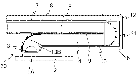
表2はリフレクタ3に遮光膜を形成しない場合の照明板5の表面を縦横に5分割した時の各分割領域の中心位置の中央分割領域に対する彩度差(ΔC*)の測定結果である。ΔC*は、CIE(国際照明委員会)が定めるL*a*b*表色系における彩度差である。表2のX1〜X25は横方向の分割領域の位置を示し、Y1〜Y5は縦方向の分割領域の位置を示す。例えば、中央分割領域はX3Y3で表される。ΔC*の値としては、顧客から5以下が要求されるが、表2においては、分割領域X1Y5の彩度差ΔC*が5.09で5を超えている。この原因は、No.2のLEDの赤色の光が強すぎるためと判明した。No.2のLEDに対向するリフレクタ3の部分の反射面に厚さ30μmで幅2mmの黒色のPETフィルムを遮光膜13Bとして貼り付けた。
Table 2 shows the measurement results of the saturation difference (ΔC * ) with respect to the central divided area at the center position of each divided area when the surface of the
表3は、この遮光膜13Bを貼り付けた場合の照明板5の各分割領域におけるΔC*の測定結果である。表3において、X1Y5のΔC*は、3.58となり、遮光膜13Bによって彩度差ΔC*が改善されたことが示されている。このように、同色(例えば赤い色)のLEDの中で最も光量の大きなLED(例えばNo.2LED)に対向するリフレクタの反射面に遮光膜を設けることで混色板4に入射する光量を低減させることができる。その結果、照明板5の表面における彩度差を小さくできる。
Table 3 shows measurement results of ΔC * in each divided region of the
次に、本発明のLCD装置の第3の実施の形態について図6を参照して説明する。 Next, a third embodiment of the LCD device of the present invention will be described with reference to FIG.
図6は、本発明の第3の実施の形態の光源装置を備えるLCD装置の要部の断面図である。図6において、図2と同じ符号のものは、図2と同じものを示す。本実施の形態では、本発明の第1の実施の形態でLED1Aに遮光膜13Aを設ける代わりに、LED1Aから出射された光の光路にある混色板4の入射面4Aに樹脂製の半透明のフィルムからなる透光量制御膜13Cを貼り付けた。半透明フィルムとしては、アクリル系樹脂、アセテート、ポリカーボネート、ポリエステル、ポリウレタンなどの光学的透明性を有する合成樹脂中に酸化アルミニウム、酸化チタンなどの光拡散性物質を分散させた形成したフィルムが使用できる。LED1Aから出射された光はリフレクタ3で反射され混色板4の入射面4Aに入射する。この入射面4Aには、透光量制御膜13Cが貼り付けられているので、LED1Aから出射された光の混色板4に導入される量が減少する。透光量制御膜13Cの厚さが厚い程、混色板4へ導入される光量は減少する。透光量制御膜13Cは、LED1Aから出射する光量が大きすぎて色度むらが発生する場合に効果を奏する。この場合、厚さや光拡散性物質の添加量を適宜調整した半透明フィルムの透光量制御膜13Cを使用することによって色度むらの発生を消失させることができる。
FIG. 6 is a cross-sectional view of a main part of an LCD device including a light source device according to a third embodiment of the present invention. 6, the same reference numerals as those in FIG. 2 denote the same elements as those in FIG. In the present embodiment, instead of providing the
次に、本発明のLCD装置の第4の実施の形態について図7を参照して説明する。 Next, a fourth embodiment of the LCD device of the present invention will be described with reference to FIG.
図7は、本発明の第4の実施の形態の光源装置を備えるLCD装置の要部の断面図である。図7において、図6と同じ符号のものは、図6と同じものを示す。本実施の形態では、本発明の第3の実施の形態でLED1を搭載する基板2の代わりに放熱板2Aを用い、さらに放熱板2Aに接して放熱フィン2Bを設けた場合である。本実施の形態では、放熱板2Aと放熱フィン2Bを使用することによって、上記の第3の実施の形態と同様な効果に併せて、LED1の温度上昇を抑制できる。なお、この放熱板2Aおよび放熱フィン2Bは、上記の第1および第2の実施の形態のLCD装置にも適用できることは言うまでもない。
FIG. 7 is a cross-sectional view of a main part of an LCD device including the light source device according to the fourth embodiment of the present invention. 7, the same reference numerals as those in FIG. 6 denote the same elements as those in FIG. In the present embodiment, the
1,1A,101 LED
2 基板
2A 放熱板
2B 放熱フィン
3,6,103,106 リフレクタ
4,104 混色板
4A,5A 入射面
4B 出射面
5,105 照明板
7,107 光学シート
8,108 LCDパネル
9,109 反射シート
10 リアカバー
11 シャーシ
12 フロントカバー
13A 遮光膜
13B 光吸収膜
13C 透光量制御膜
20,120 光源装置
110 アルミニウムフレーム
111 固定具
1,1A, 101 LED
2
Claims (13)
Priority Applications (3)
| Application Number | Priority Date | Filing Date | Title |
|---|---|---|---|
| JP2006340613A JP4816437B2 (en) | 2006-01-04 | 2006-12-19 | Light source device and liquid crystal display device using the same |
| US11/647,238 US7585098B2 (en) | 2006-01-04 | 2006-12-29 | Light source device and liquid crystal display device using the same |
| CN2007100022547A CN1996129B (en) | 2006-01-04 | 2007-01-04 | Light source device and liquid crystal display device using the same |
Applications Claiming Priority (3)
| Application Number | Priority Date | Filing Date | Title |
|---|---|---|---|
| JP2006000192 | 2006-01-04 | ||
| JP2006000192 | 2006-01-04 | ||
| JP2006340613A JP4816437B2 (en) | 2006-01-04 | 2006-12-19 | Light source device and liquid crystal display device using the same |
Publications (2)
| Publication Number | Publication Date |
|---|---|
| JP2007207751A JP2007207751A (en) | 2007-08-16 |
| JP4816437B2 true JP4816437B2 (en) | 2011-11-16 |
Family
ID=38224165
Family Applications (1)
| Application Number | Title | Priority Date | Filing Date |
|---|---|---|---|
| JP2006340613A Active JP4816437B2 (en) | 2006-01-04 | 2006-12-19 | Light source device and liquid crystal display device using the same |
Country Status (3)
| Country | Link |
|---|---|
| US (1) | US7585098B2 (en) |
| JP (1) | JP4816437B2 (en) |
| CN (1) | CN1996129B (en) |
Families Citing this family (13)
| Publication number | Priority date | Publication date | Assignee | Title |
|---|---|---|---|---|
| CN101346581B (en) * | 2006-04-19 | 2010-05-19 | 夏普株式会社 | Backlight device and display using it |
| US20090303708A1 (en) * | 2006-04-21 | 2009-12-10 | Koninklijke Philips Electronics N V | Illumination System |
| JP2007329073A (en) * | 2006-06-09 | 2007-12-20 | Mitsubishi Electric Corp | Planar light source device |
| US20080191904A1 (en) * | 2007-02-12 | 2008-08-14 | Kai-Jie Tsao | Method For Manufacturing Thin Keypad Assembly And Such Assembly |
| JP5413769B2 (en) * | 2007-09-13 | 2014-02-12 | Nltテクノロジー株式会社 | Backlight and liquid crystal display device |
| CN102269387B (en) * | 2010-06-01 | 2013-08-28 | 中强光电股份有限公司 | Light guiding unit and light source module |
| US8534901B2 (en) * | 2010-09-13 | 2013-09-17 | Teledyne Reynolds, Inc. | Collimating waveguide apparatus and method |
| US9244299B2 (en) * | 2011-11-22 | 2016-01-26 | Shenzhen China Star Optoelectronics Technology Co., Ltd. | Backlight module of display device |
| US9805630B2 (en) * | 2012-03-09 | 2017-10-31 | Apple Inc. | Light guide structures for display backlights |
| TWI451170B (en) * | 2012-04-10 | 2014-09-01 | Au Optronics Corp | Display apparatus with narrowed board and manufacturing method thereof |
| TW201426039A (en) * | 2012-12-26 | 2014-07-01 | Hon Hai Prec Ind Co Ltd | Light guide plate |
| CN103697376A (en) * | 2013-12-09 | 2014-04-02 | 京东方科技集团股份有限公司 | Backlight source and display device |
| US10690837B2 (en) | 2016-06-21 | 2020-06-23 | Apple Inc. | Backlist displays with bent light guide layers |
Family Cites Families (13)
| Publication number | Priority date | Publication date | Assignee | Title |
|---|---|---|---|---|
| JP2975494B2 (en) * | 1993-01-28 | 1999-11-10 | シャープ株式会社 | Backlight device and liquid crystal display device |
| JPH08234200A (en) * | 1995-02-28 | 1996-09-13 | Japan Aviation Electron Ind Ltd | Backlight for liquid crystal |
| US6608332B2 (en) * | 1996-07-29 | 2003-08-19 | Nichia Kagaku Kogyo Kabushiki Kaisha | Light emitting device and display |
| JP2000010094A (en) * | 1998-06-19 | 2000-01-14 | Nec Corp | Backlight device |
| JP3758878B2 (en) * | 1999-02-12 | 2006-03-22 | 松下電器産業株式会社 | Mobile terminal device |
| JP2000331522A (en) * | 1999-05-21 | 2000-11-30 | Matsushita Electric Ind Co Ltd | Lighting system and liquid crystal display device |
| US6352350B1 (en) * | 2000-06-01 | 2002-03-05 | Agilent Technologies, Inc. | High efficiency flat illuminator for liquid crystal micro-display |
| EP1324620A3 (en) * | 2001-12-28 | 2005-01-05 | Sony Corporation | Display apparatus |
| CN1226651C (en) * | 2002-07-22 | 2005-11-09 | 致伸科技股份有限公司 | Optical source colour-adjusting apparatus and method |
| US20040061810A1 (en) | 2002-09-27 | 2004-04-01 | Lumileds Lighting, U.S., Llc | Backlight for a color LCD using wavelength-converted light emitting devices |
| JP4156919B2 (en) | 2002-12-18 | 2008-09-24 | 三菱電機株式会社 | Planar light source device, liquid crystal display device, and display device |
| JP2005332719A (en) * | 2004-05-20 | 2005-12-02 | Mitsubishi Electric Corp | Planar light source device and display device having planar light source device |
| US7237938B2 (en) * | 2005-03-25 | 2007-07-03 | Harvatek Corporation | Backlight module |
-
2006
- 2006-12-19 JP JP2006340613A patent/JP4816437B2/en active Active
- 2006-12-29 US US11/647,238 patent/US7585098B2/en active Active
-
2007
- 2007-01-04 CN CN2007100022547A patent/CN1996129B/en active Active
Also Published As
| Publication number | Publication date |
|---|---|
| US20070153539A1 (en) | 2007-07-05 |
| US7585098B2 (en) | 2009-09-08 |
| JP2007207751A (en) | 2007-08-16 |
| CN1996129B (en) | 2012-12-12 |
| CN1996129A (en) | 2007-07-11 |
Similar Documents
| Publication | Publication Date | Title |
|---|---|---|
| JP4816437B2 (en) | Light source device and liquid crystal display device using the same | |
| JP4677746B2 (en) | Backlight device | |
| JP4765837B2 (en) | Backlight device and liquid crystal display device | |
| US7465082B2 (en) | Planar light-source device | |
| JP4604801B2 (en) | Planar light source device and display device using the same | |
| JP4790651B2 (en) | Surface light source device and display device using the surface light source device | |
| JP2006024439A (en) | Surface light source device | |
| JP2007180021A (en) | Light guide member and plane light source device provided with this light guide member, and display device using this plane light source device | |
| US20120249885A1 (en) | Lighting device, display device and television receiver | |
| JP2004199967A (en) | Planar light source device, liquid crystal display device, and display device | |
| KR102613460B1 (en) | Display appartus | |
| US20200379298A1 (en) | Lighting device and liquid crystal display apparatus | |
| JP2005222814A (en) | Surface light source device and display device using the same | |
| MX2012009374A (en) | Lighting device, display apparatus, and television receiver. | |
| US20160363716A1 (en) | Display device | |
| JP5899722B2 (en) | Planar light source device and display device | |
| CN108700772B (en) | Display device | |
| JP2009026635A (en) | Lighting system, and liquid crystal display device | |
| JP2007214081A (en) | Lighting device and display device | |
| US20080291694A1 (en) | Planar light source device and display device | |
| WO2011077864A1 (en) | Illumination device, display device, and television receiver | |
| JP2006133583A (en) | Liquid crystal display device | |
| JP7446065B2 (en) | display device | |
| US11194189B2 (en) | Display apparatus | |
| WO2012102096A1 (en) | Edge-light type lighting apparatus and display apparatus |
Legal Events
| Date | Code | Title | Description |
|---|---|---|---|
| RD01 | Notification of change of attorney |
Free format text: JAPANESE INTERMEDIATE CODE: A7421 Effective date: 20080618 |
|
| RD01 | Notification of change of attorney |
Free format text: JAPANESE INTERMEDIATE CODE: A7421 Effective date: 20090602 |
|
| A621 | Written request for application examination |
Free format text: JAPANESE INTERMEDIATE CODE: A621 Effective date: 20091027 |
|
| A711 | Notification of change in applicant |
Free format text: JAPANESE INTERMEDIATE CODE: A711 Effective date: 20100312 |
|
| A977 | Report on retrieval |
Free format text: JAPANESE INTERMEDIATE CODE: A971007 Effective date: 20110214 |
|
| A131 | Notification of reasons for refusal |
Free format text: JAPANESE INTERMEDIATE CODE: A131 Effective date: 20110308 |
|
| A521 | Request for written amendment filed |
Free format text: JAPANESE INTERMEDIATE CODE: A523 Effective date: 20110421 |
|
| RD01 | Notification of change of attorney |
Free format text: JAPANESE INTERMEDIATE CODE: A7421 Effective date: 20110705 |
|
| TRDD | Decision of grant or rejection written | ||
| A01 | Written decision to grant a patent or to grant a registration (utility model) |
Free format text: JAPANESE INTERMEDIATE CODE: A01 Effective date: 20110802 |
|
| A01 | Written decision to grant a patent or to grant a registration (utility model) |
Free format text: JAPANESE INTERMEDIATE CODE: A01 |
|
| A61 | First payment of annual fees (during grant procedure) |
Free format text: JAPANESE INTERMEDIATE CODE: A61 Effective date: 20110815 |
|
| FPAY | Renewal fee payment (event date is renewal date of database) |
Free format text: PAYMENT UNTIL: 20140909 Year of fee payment: 3 |
|
| R150 | Certificate of patent or registration of utility model |
Ref document number: 4816437 Country of ref document: JP Free format text: JAPANESE INTERMEDIATE CODE: R150 Free format text: JAPANESE INTERMEDIATE CODE: R150 |
|
| FPAY | Renewal fee payment (event date is renewal date of database) |
Free format text: PAYMENT UNTIL: 20140909 Year of fee payment: 3 |
|
| S111 | Request for change of ownership or part of ownership |
Free format text: JAPANESE INTERMEDIATE CODE: R313113 |
|
| FPAY | Renewal fee payment (event date is renewal date of database) |
Free format text: PAYMENT UNTIL: 20140909 Year of fee payment: 3 |
|
| R360 | Written notification for declining of transfer of rights |
Free format text: JAPANESE INTERMEDIATE CODE: R360 |
|
| R360 | Written notification for declining of transfer of rights |
Free format text: JAPANESE INTERMEDIATE CODE: R360 |
|
| R371 | Transfer withdrawn |
Free format text: JAPANESE INTERMEDIATE CODE: R371 |
|
| S111 | Request for change of ownership or part of ownership |
Free format text: JAPANESE INTERMEDIATE CODE: R313113 |
|
| R350 | Written notification of registration of transfer |
Free format text: JAPANESE INTERMEDIATE CODE: R350 |
|
| R250 | Receipt of annual fees |
Free format text: JAPANESE INTERMEDIATE CODE: R250 |
|
| R250 | Receipt of annual fees |
Free format text: JAPANESE INTERMEDIATE CODE: R250 |
|
| R250 | Receipt of annual fees |
Free format text: JAPANESE INTERMEDIATE CODE: R250 |
|
| R250 | Receipt of annual fees |
Free format text: JAPANESE INTERMEDIATE CODE: R250 |
|
| R250 | Receipt of annual fees |
Free format text: JAPANESE INTERMEDIATE CODE: R250 |
|
| R250 | Receipt of annual fees |
Free format text: JAPANESE INTERMEDIATE CODE: R250 |
|
| R250 | Receipt of annual fees |
Free format text: JAPANESE INTERMEDIATE CODE: R250 |
|
| R250 | Receipt of annual fees |
Free format text: JAPANESE INTERMEDIATE CODE: R250 |
|
| R250 | Receipt of annual fees |
Free format text: JAPANESE INTERMEDIATE CODE: R250 |
|
| S111 | Request for change of ownership or part of ownership |
Free format text: JAPANESE INTERMEDIATE CODE: R313113 |
|
| R350 | Written notification of registration of transfer |
Free format text: JAPANESE INTERMEDIATE CODE: R350 |
|
| RD02 | Notification of acceptance of power of attorney |
Free format text: JAPANESE INTERMEDIATE CODE: R3D02 |
|
| R250 | Receipt of annual fees |
Free format text: JAPANESE INTERMEDIATE CODE: R250 |