JP4815571B2 - Enhanced bit mapping for digital interfaces of wireless communication devices in multi-time slot and multi-mode operation - Google Patents
Enhanced bit mapping for digital interfaces of wireless communication devices in multi-time slot and multi-mode operation Download PDFInfo
- Publication number
- JP4815571B2 JP4815571B2 JP2007523186A JP2007523186A JP4815571B2 JP 4815571 B2 JP4815571 B2 JP 4815571B2 JP 2007523186 A JP2007523186 A JP 2007523186A JP 2007523186 A JP2007523186 A JP 2007523186A JP 4815571 B2 JP4815571 B2 JP 4815571B2
- Authority
- JP
- Japan
- Prior art keywords
- modulator
- baseband
- interface
- digital interface
- control device
- Prior art date
- Legal status (The legal status is an assumption and is not a legal conclusion. Google has not performed a legal analysis and makes no representation as to the accuracy of the status listed.)
- Expired - Fee Related
Links
Images


Classifications
-
- H—ELECTRICITY
- H04—ELECTRIC COMMUNICATION TECHNIQUE
- H04L—TRANSMISSION OF DIGITAL INFORMATION, e.g. TELEGRAPHIC COMMUNICATION
- H04L27/00—Modulated-carrier systems
-
- H—ELECTRICITY
- H04—ELECTRIC COMMUNICATION TECHNIQUE
- H04L—TRANSMISSION OF DIGITAL INFORMATION, e.g. TELEGRAPHIC COMMUNICATION
- H04L27/00—Modulated-carrier systems
- H04L27/0008—Modulated-carrier systems arrangements for allowing a transmitter or receiver to use more than one type of modulation
-
- H—ELECTRICITY
- H04—ELECTRIC COMMUNICATION TECHNIQUE
- H04B—TRANSMISSION
- H04B1/00—Details of transmission systems, not covered by a single one of groups H04B3/00 - H04B13/00; Details of transmission systems not characterised by the medium used for transmission
- H04B1/06—Receivers
- H04B1/16—Circuits
- H04B1/20—Circuits for coupling gramophone pick-up, recorder output, or microphone to receiver
-
- H—ELECTRICITY
- H04—ELECTRIC COMMUNICATION TECHNIQUE
- H04B—TRANSMISSION
- H04B1/00—Details of transmission systems, not covered by a single one of groups H04B3/00 - H04B13/00; Details of transmission systems not characterised by the medium used for transmission
- H04B1/38—Transceivers, i.e. devices in which transmitter and receiver form a structural unit and in which at least one part is used for functions of transmitting and receiving
- H04B1/40—Circuits
-
- H—ELECTRICITY
- H04—ELECTRIC COMMUNICATION TECHNIQUE
- H04B—TRANSMISSION
- H04B7/00—Radio transmission systems, i.e. using radiation field
- H04B7/005—Control of transmission; Equalising
-
- H—ELECTRICITY
- H04—ELECTRIC COMMUNICATION TECHNIQUE
- H04W—WIRELESS COMMUNICATION NETWORKS
- H04W52/00—Power management, e.g. TPC [Transmission Power Control], power saving or power classes
- H04W52/04—TPC
Abstract
Description
本発明は、無線通信機器のデジタル・ベースバンド伝送路に関し、より厳密には、デジタル・インターフェースを介するこのような機器の変調装置および/または利得制御装置の制御に関する。 The present invention relates to a digital baseband transmission line of a wireless communication device, and more specifically to control of a modulation device and / or a gain control device of such device via a digital interface.
GSM(Global System for Mobile communications:移動体通信のためのグローバル・システム)などの特定の通信ネットワークにおいて、いわゆるEGPRS(Enhanced General Packet Radio Service:拡張型汎用パケット無線サービス)規格などの新しい規格によってデータ・レートを向上させることが提案されてきた。たとえば、EGPRS規格はGSMネットワークに8PSK(8 Phase Shift Keying:8位相偏移変調)と呼ばれる新しい変調手法を取り入れて、GMSK(Gaussian Minimum Shift Keying:ガウス最小偏移変調)変調手法により前もって提供されたデータ・レートを向上させる。 In specific communication networks such as GSM (Global System for Mobile communications), data and data can be updated by new standards such as the so-called EGPRS (Enhanced General Packet Radio Service) standard. It has been proposed to improve the rate. For example, the EGPRS standard was previously provided by a GMSK (Gaussian Minimum Shift Keying) modulation technique, incorporating a new modulation technique called 8PSK (8 Phase Shift Keying) into the GSM network. Increase data rate.
データ伝送の柔軟性のため、EGPRS規格は多タイム・スロット(すなわちマルチスロット)を定義し、およびGSMフレームを分割する8個のタイム・スロットのうちの1つより多いタイム・スロットを必要とする多モード動作が、GMSKまたは8PSK変調を伴うデータ伝送のために使用され得る。したがって、EGPRS無線通信機器は、連続したタイム・スロットにおいてGMSK変調手法から8PSK変調手法に、またその逆に容易に切り換えることができる変調器を備えなければならない。 For data transmission flexibility, the EGPRS standard defines multiple time slots (ie, multislots) and requires more than one of the eight time slots that divide a GSM frame. Multi-mode operation may be used for data transmission with GMSK or 8PSK modulation. Therefore, EGPRS wireless communication equipment must be equipped with a modulator that can be easily switched from a GMSK modulation scheme to an 8PSK modulation scheme and vice versa in successive time slots.
しかし、当業者には知られているように、GMSKは、高効率を伴う飽和電力増幅の使用を可能とする定包絡線変調手法であり、8PSKは、位相だけでなく振幅も変化する変調された搬送波を供給する変調手法であり、したがって、線形振幅を除いては、飽和電力増幅の使用を可能とし得ない。 However, as is known to those skilled in the art, GMSK is a constant envelope modulation technique that allows the use of saturated power amplification with high efficiency, and 8PSK is a modulated that varies not only in phase but also in amplitude. Modulation scheme that supplies a separate carrier wave, and therefore cannot allow the use of saturation power amplification except for linear amplitude.
したがって、マルチスロット動作では変調手法は変化するが、多分電力振幅モードも変化し、それは残念ながら、連続したタイム・スロットに関連する隣接チャネル間の干渉を生じさせる。 Thus, in multi-slot operation, the modulation scheme changes, but perhaps the power amplitude mode also changes, which unfortunately causes interference between adjacent channels associated with successive time slots.
これらの干渉を低減させるために、電力増幅器の利得制御装置を用いて送信電力を傾斜減少させ、連続したタイム・スロット間に設けられた保護期間中に変調器および/または電力増幅モードを変更させることが提案されてきた。保護期間は、データ伝送なしの制御および/または切換え動作に専用の時間間隔であることが思い出されよう。 To reduce these interferences, the power amplifier gain controller is used to ramp down transmit power and change the modulator and / or power amplification mode during the protection period provided between successive time slots. It has been proposed. It will be recalled that the protection period is a time interval dedicated to control and / or switching operations without data transmission.
この解決策の代替案が、特に特許文献第WO 2004/021659号に記載されている。それは、電力増幅モードも復調器も変更しないI/Q信号の整形(ただしIおよびQは、それぞれ同相および直交成分である)による電力のランピング[ramping―傾斜をもつ変化―]に適応された結合GMSK/8PSK・I/Q変調器から成る。これは、結合GMSK/8PSK・I/Q変調器にゼロを供給することによって行なわれ、それによってI/Q信号の電力の制御を可能にする。 An alternative to this solution is described in particular in patent document WO 2004/021659. It is a combination adapted to power ramping by shaping I / Q signals (where I and Q are in-phase and quadrature components, respectively) without changing the power amplification mode or demodulator It consists of a GMSK / 8PSK I / Q modulator. This is done by supplying a zero to the combined GMSK / 8PSK I / Q modulator, thereby allowing control of the power of the I / Q signal.
外部電力制御ループが使用される場合、変調器機能が電力制御ループから切り離されること、または換言すると、電力増幅器のランピングが変調器の動作によってではなく、厳密には電力制御ループによって決定されることが必要とされる。この厳しい状況は、変調器出力信号が滑らかな遷移ではなく、オン/オフ状態(データ・モード対強制ゼロ・モード)間で瞬時の遷移を有することを必要とする。こうした遷移は、変調切換えならびに利得切換えが正確でタイミングが合わせられることを必要とする。 If an external power control loop is used, the modulator function is disconnected from the power control loop, or in other words, the power amplifier ramping is determined strictly by the power control loop, not by the operation of the modulator. Is needed. This severe situation requires the modulator output signal to have an instantaneous transition between on / off states (data mode versus forced zero mode) rather than a smooth transition. Such transitions require modulation switching as well as gain switching to be accurate and timed.
工業規格が、デジタル・ベースバンド・プロセッサ(すなわちデバイス)、ベースバンド・インターフェース(すなわちBAI)、および(電力増幅器(すなわちPA)に接続された)無線周波数(RF)デバイスの間のインターフェースを標準化するために提案されてきた。 Industry standards standardize the interface between digital baseband processors (ie devices), baseband interfaces (ie BAI), and radio frequency (RF) devices (connected to power amplifiers (ie PA)) Has been proposed for.
送信方向について、デジタル・ベースバンド・プロセッサは、デジタル信号プロセッサ(DSP:digital signal processor)と、BAIにインターフェースするコントローラ・デバイス(ARMなど)とを主に備え、ベースバンド・インターフェース(すなわちBAI)は、変調器と、利得制御装置と、デジタル・アナログ変換器(すなわちDAC)と、無線周波数(RF)デバイスにインターフェースするポストフィルタとを主に備え、RFデバイスは、フィルタと、利得段と、ミキサとを主に備えることが思い出される。デジタル・ベースバンド・プロセッサ(すなわちデバイス)と、ベースバンド・インターフェース(すなわちBAI)と、無線周波数(RF)デバイスと、電力増幅器(すなわちPA)は、無線通信機器の伝送路と呼ばれるものを定義する。 For the transmit direction, the digital baseband processor mainly comprises a digital signal processor (DSP) and a controller device (such as ARM) that interfaces to the BAI, where the baseband interface (ie BAI) is A modulator, a gain controller, a digital-to-analog converter (or DAC), and a post filter that interfaces to a radio frequency (RF) device, the RF device comprising a filter, a gain stage, and a mixer It is remembered to prepare mainly. A digital baseband processor (ie device), a baseband interface (ie BAI), a radio frequency (RF) device, and a power amplifier (ie PA) define what is referred to as the transmission path of a wireless communication device. .
デジタル・ベースバンド・プロセッサ、BAIおよびRFデバイスは、同じチップ上で定義されてもよく、別個のチップ上で定義されてもよく、これらの3つのデバイスのうちの2つの任意の組合せもまた、同じチップ上で定義されてもよい。したがって、それらは「チップ間接続モード」、または「ブロック間接続モード」(それらが同じチップ上に集積化される場合)で互いに接続されてもよい。しかし、どの接続モードであってもそれらは、デジタル・インターフェースを介してインターフェースされることが必要である。 The digital baseband processor, BAI and RF devices may be defined on the same chip or on separate chips, and any combination of two of these three devices can also be It may be defined on the same chip. Thus, they may be connected to each other in “interchip connection mode” or “interblock connection mode” (when they are integrated on the same chip). However, in any connection mode they need to be interfaced via a digital interface.
工業規格は、「デジタルRFインターフェース」と呼ばれており、「digRF」という名前のプロトコルを実行することができるデジタル・インターフェース、およびベースバンド・デバイスとベースバンド・インターフェース(すなわちBAI)の間のデータ伝送を容易にするための制御デバイスを定義する。これは、制御デバイス内に格納されており、無線周波数デバイス用のシンボルとデジタル・インターフェースを介してこの無線周波数デバイスに送信するために符号化値との間の対応を確立している符号化テーブルを用いて行なわれる。 The industry standard is called “digital RF interface”, a digital interface capable of implementing a protocol named “digRF”, and data between a baseband device and a baseband interface (ie BAI). Define a control device to facilitate transmission. This is an encoding table which is stored in the control device and establishes a correspondence between the symbol for the radio frequency device and the encoded value for transmission to this radio frequency device via the digital interface It is performed using.
たとえば、GMSK/8PSK・I/Q変調器の場合、符号化テーブルは16個のシンボルを備え、2個がGMSK・I/Q変調器に供給するためのデータ・ワードに対応し、8個が8PSK・I/Q変調器に供給するためのデータ・ワードに対応し、最後の6個が独自の使用(proprietary use)のために使用される。 For example, in the case of a GMSK / 8PSK I / Q modulator, the coding table comprises 16 symbols, 2 corresponding to data words for supply to the GMSK I / Q modulator, and 8 Corresponding to the data word to supply to the 8PSK I / Q modulator, the last six are used for proprietary use.
デジタル・インターフェース、digRFプロトコルおよびその環境についてのいくらかのさらなる情報は、インターネット・アドレス「www.digrf.com」で、たとえば文献「DigRF, Baseband / RF digital interface specification : Logical, Electrical and timing characteristics」、第1.12版で見られてもよい。 Some additional information about the digital interface, the digRF protocol and its environment can be found at the Internet address “www.digrf.com”, eg the document “DigRF, Baseband / RF digital interface specification: Logical, Electrical and timing characteristics” You may be seen in the 1.12 version.
この工業規格はまだ十分ではない。したがって、本発明の目的は、その状況を改善することである。 This industry standard is not enough. The object of the present invention is therefore to improve the situation.
このためそれは、無線通信機器のベースバンド・デバイスとベースバンド・インターフェース・デバイス(すなわちBAIデバイス)(利得制御装置への供給を行なう少なくとも変調器を備える)とを接続するデジタル・インターフェースに符号化された値を送信することの制御に専用であり、BAIデバイス用のシンボルとデジタル・インターフェースを介したBAIデバイスへの送信のための符号化値との間の対応を確立する符号化テーブルを格納する格納手段を備える制御デバイスを提供する。 For this purpose, it is encoded into a digital interface that connects the baseband device of the wireless communication equipment and the baseband interface device (ie BAI device) (with at least a modulator to supply the gain controller). A coding table that is dedicated to controlling the transmission of the received value and establishes a correspondence between the symbol for the BAI device and the coded value for transmission to the BAI device via the digital interface A control device comprising a storage means is provided.
この制御装置は、その符号化テーブルが、変調器に供給するためのデータ・ワードを備える第1のシンボル群と、変調器および/または利得制御装置の動作を制御するためのコマンド・ワードを備える第2のシンボル群とを備えることを特徴とするが、それがベースバンド・デバイスからシンボルを受信するときにそれがデジタル・インターフェースを介して無線周波数デバイスに送信され得るように、格納手段内でこのシンボルに対応する符号化された値を決定するように構成された制御手段を備えることをも特徴とする。 The controller comprises a first symbol group whose coding table comprises a data word for supply to the modulator and a command word for controlling the operation of the modulator and / or gain controller. In the storage means so that when it receives a symbol from the baseband device, it can be transmitted to the radio frequency device via the digital interface when it receives the symbol from the baseband device. It is also characterized in that it comprises control means arranged to determine an encoded value corresponding to this symbol.
換言すると、本発明は、変調器にデータおよび残りのシンボルを供給するために符号化テーブルに格納されており、またデジタル・インターフェースを介して変調器および/または利得制御装置にコマンドを送信するために符号化テーブルに格納されているシンボルの一部を使用することを提供する。 In other words, the present invention is stored in a coding table for supplying data and remaining symbols to the modulator, and for sending commands to the modulator and / or gain controller via the digital interface. To use a part of the symbol stored in the encoding table.
本発明による制御デバイスは、個々にまたは組み合わせて考慮される追加の特性、特に以下を含んでもよい。
−第2群のシンボルのうちの少なくとも1つが、選択された利得値を利得制御装置に割り当てるためのコマンド・ワードであってもよい。
−第2群のシンボルのうちの少なくとも1つが、選択された動作モードを変調器のフィルタ手段および/または変調手段に割り当てるためのコマンド・ワードであってもよい。
−第2群のシンボルのうちの少なくとも1つが、選択された動作モードを変調器のフィルタ手段および/または変調手段に、また選択された利得値を利得制御装置に割り当てるためのコマンド・ワードであってもよい。
−動作モードは、たとえば、変調器の即時の立上げのためフィルタ手段に回転された有効シンボルの選択されたシーケンスを事前ロードするための「初期化モード」、あるいはゼロの2進値を変調器のフィルタの遅延鎖に強制的に入れるための「再設定モード」(すべての遅延をゼロにして、ゼロ出力への急激な遷移、すなわち変調器の即時の立下げをもたらす)、そうでない場合は、少なくとも1つのゼロの2進値を変調器に強制的に入れるための「強制ゼロ・モード」(入力において滑らかな立下げ/立上げをもたらす)であってもよい。この場合、制御デバイスは、保護間隔を埋める最後の保護ビットをフィルタ手段に送信する前に初期化モードを割り当てるためのコマンド・ワードを供給し、かつ/またはデータ・バーストのアクティブ部分をフィルタ手段に送信する直後および保護期間中に再設定モードを割り当てるためのコマンド・ワードを供給するように構成されてもよい。
−変調器がGMSK・I/Q変調器と8PSK・I/Q変調器とを備える場合、符号化された各値は、3つの最上位ビット(MSB:most significant bit)と、GMSK・I/Q変調器を8PSK・I/Q変調器と区別するための1つの下位ビット(LSB:low significant bit)とを備える4ビット・ワードであってもよい。この場合、第1群は少なくとも8つのシンボルを備えてもよく、第2群は少なくとも6つのシンボルを備えてもよい。
The control device according to the invention may include additional properties that are considered individually or in combination, in particular:
-At least one of the second group of symbols may be a command word for assigning the selected gain value to the gain controller;
At least one of the second group of symbols may be a command word for assigning the selected mode of operation to the filter means and / or modulation means of the modulator.
-At least one of the symbols of the second group is a command word for assigning the selected operating mode to the filter means and / or modulator means of the modulator and the selected gain value to the gain controller; May be.
The operating mode is, for example, an “initialization mode” for preloading a selected sequence of valid symbols rotated to the filter means for the immediate start-up of the modulator, or a binary value of zero A "reset mode" to force the filter into the delay chain of the filter (zeroing all delays, resulting in a sudden transition to zero output, ie, an immediate fall of the modulator), otherwise May be a “forced zero mode” to force at least one binary binary value into the modulator (resulting in a smooth fall / rise at the input). In this case, the control device supplies a command word for assigning an initialization mode before sending the last protection bit to fill the protection interval to the filter means and / or the active part of the data burst to the filter means. It may be configured to provide a command word for assigning a reset mode immediately after transmission and during the protection period.
If the modulator comprises a GMSK • I / Q modulator and an 8PSK • I / Q modulator, each encoded value consists of three most significant bits (MSB) and a GMSK • I / It may be a 4-bit word with one low significant bit (LSB) for distinguishing the Q modulator from the 8PSK · I / Q modulator. In this case, the first group may comprise at least 8 symbols and the second group may comprise at least 6 symbols.
本発明は、デジタル・インターフェースを介してベースバンド・デバイスに接続されるように適応されたBAIデバイスを備え、また上記で述べられた制御デバイスなどの制御デバイスを備える無線通信機器用の前記ベースバンド・デバイスをも提供する。 The present invention comprises a BAI device adapted to be connected to a baseband device via a digital interface, and said baseband for a wireless communication device comprising a control device, such as the control device described above・ Provide devices.
本発明は、上記で述べられたベースバンド・デバイスなどのベースバンド・デバイスを備え、デジタル・インターフェースを介してBAIデバイスに接続されるように適応された無線通信機器用のベースバンド・インターフェース・デバイス(すなわちBAIデバイス)をも提供する。このBAIデバイスは、少なくとも変調器と、変調器からの供給を受ける利得制御装置と、デジタル・インターフェースによって送信される符号化値と、その動作を制御するためのコマンド・ワードを表すシンボルおよび変調器に供給するためのデータ・ワードとの間の対応を確立する制御テーブルを格納するように構成された格納手段と、デジタル・インターフェース、変調器および利得制御装置に結合されており、それがデジタル・インターフェースから符号化値を受信するときにそれを変調器および/または利得制御装置に送信するため、格納手段内で受信された符号化値に対応するワードを決定するように構成された制御手段とを備える。 The present invention comprises a baseband interface device for wireless communication equipment comprising a baseband device, such as the baseband device described above, adapted to be connected to a BAI device via a digital interface (Ie BAI devices) are also provided. The BAI device includes at least a modulator, a gain control device supplied by the modulator, a coded value transmitted by a digital interface, and a symbol and a modulator representing a command word for controlling the operation thereof Is coupled to a storage means configured to store a control table that establishes a correspondence between data words for supply to a digital interface, a modulator and a gain control device, Control means configured to determine a word corresponding to the received encoded value in the storage means for transmitting the encoded value from the interface to the modulator and / or gain controller when receiving the encoded value; Is provided.
代替法では、BAIデバイスは、デジタル・インターフェースを介してそれに接続されたベースバンド・デバイスと、上記で述べられた制御デバイスなどの制御デバイスとを備える無線通信機器に専用である。 In the alternative, the BAI device is dedicated to wireless communication equipment comprising a baseband device connected to it via a digital interface and a control device such as the control device described above.
ベースバンド・デバイス、BAIデバイスおよびRFデバイスが同じチップ上で定義されても、個別のチップ上で定義されてもよく、これらの3つのデバイスのうちの2つの任意の組合せもまた同じチップ上で定義されてもよいことに留意されたい。しかし、構成がどうであれ、これらのデバイスは、上述のデジタル・インターフェースを使用しなければならない。 Baseband devices, BAI devices and RF devices may be defined on the same chip or on separate chips, and any combination of two of these three devices may also be defined on the same chip. Note that it may be defined. However, whatever the configuration, these devices must use the digital interface described above.
本発明は、ベースバンド・デバイスとデジタル・インターフェースと、上記で述べられた制御デバイスなどの制御デバイスと、デジタル・インターフェースを介してベースバンド・デバイスに接続された、上記で述べられたBAIデバイスなどのBAIデバイスと、BAIデバイスに接続されたRFデバイスとを備える無線通信装置をも提供する。 The present invention includes a baseband device and a digital interface; a control device such as the control device described above; a BAI device as described above connected to the baseband device via a digital interface; There is also provided a wireless communication apparatus including a BAI device and an RF device connected to the BAI device.
代替法では、無線通信機器は、上記で述べられたベースバンド・デバイスなどのベースバンド・デバイスと、デジタル・インターフェースと、デジタル・インターフェースを介してベースバンド・デバイスに接続された、上記で述べられたBAIデバイスなどのBAIデバイスと、BAIデバイスに接続されたRFデバイスとを備えてもよい。 In the alternative, the wireless communication device is described above, connected to a baseband device such as the baseband device described above, a digital interface, and the baseband device via the digital interface. A BAI device such as a BAI device and an RF device connected to the BAI device may be provided.
こうした機器は、たとえば携帯電話であってもよい。 Such a device may be, for example, a mobile phone.
本発明の他の特徴および利点は、以下の詳細な仕様および添付の図面を精査すると明らかになろう。 Other features and advantages of the present invention will become apparent upon review of the following detailed specification and accompanying drawings.
添付の図面は、本発明を完全なものにするのに役立つだけでなく、必要であればその定義に寄与することもある。 The accompanying drawings not only serve to complete the invention, but may also contribute to its definition if necessary.
上述され、また図1に概略的に示されているように、無線通信機器のデジタル・ベースバンド伝送路が、デジタル・ベースバンド・プロセッサ(すなわちデバイス)BBDと、少なくとも変調器Mと利得制御装置GCと、デジタル・インターフェースIを介してデジタル・ベースバンド・デバイスBBDに接続されたデジタル・アナログ変換器DACフィルタとを備えるベースバンド・インターフェース・デバイスBAIとを備えている。デジタル・ベースバンド伝送路は、アンテナANに接続された電力増幅器PAにそれ自体が接続される無線周波数(RF)デバイスRFDに接続される。デジタル・ベースバンド伝送路、無線周波数(RF)デバイスRFDおよび電力増幅器PAは、伝送路を構成する。 As described above and schematically illustrated in FIG. 1, a digital baseband transmission path of a wireless communication device includes a digital baseband processor (ie, device) BBD, at least a modulator M, and a gain controller. A baseband interface device BAI comprising a GC and a digital-to-analog converter DAC filter connected to the digital baseband device BBD via the digital interface I; The digital baseband transmission line is connected to a radio frequency (RF) device RFD that itself is connected to a power amplifier PA connected to an antenna AN. The digital baseband transmission line, the radio frequency (RF) device RFD, and the power amplifier PA constitute a transmission line.
デジタル・ベースバンド伝送路の利得段は通常分散され、一部は(デジタルまたはアナログの形で)ベースバンド・インターフェース・デバイスBAI内に置かれた利得制御装置GCを備え、別の部分は(アナログの形で)RFデバイスRFD内に置かれることに留意されたい。 The gain stage of a digital baseband transmission line is usually distributed, with a gain controller GC located partly (in digital or analog form) in the baseband interface device BAI and another part (analog Note that it is placed in the RF device RFD.
以降の説明では、デジタル・インターフェースIは、上記で引用された文献「DigRF, Baseband / RF digital interface specification : Logical, Electrical and timing characteristics」、第1.12版で述べられているインターフェースのタイプのものであることが考慮されるであろう。したがって、以降の説明では、例示的な実施例として、デジタル・インターフェースIはdigRFプロトコル・スタックの少なくとも一部を実行できることが考慮されるであろう。 In the following description, the digital interface I is of the interface type described in the above-cited document "DigRF, Baseband / RF digital interface specification: Logical, Electrical and timing characteristics", version 1.12. Will be considered. Accordingly, in the description that follows, as an exemplary embodiment, it will be considered that the digital interface I can execute at least a portion of the digRF protocol stack.
しかし、本発明は、この種類のデジタル・インターフェースに限定されない。 However, the invention is not limited to this type of digital interface.
さらに、以降の説明では、(実施形態の非限定な例において)ベースバンド・インターフェース・デバイスBAIは、ベースバンドおよびオーディオ・インターフェース・デバイスであることが考慮されるであろう。 Further, in the description that follows, it will be considered that (in a non-limiting example of embodiment) the baseband interface device BAI is a baseband and audio interface device.
さらに、以降の説明では、変調器Mは、EGPRS(またはEDGE)標準に準拠した拡張型データ・レートを伴うGSM携帯電話など、無線通信装置内に設置された結合8PSK/GMSK・I/Q変調器であることが考慮されるであろう。換言すると、変調器Mは、多モード動作においてGSMフレームの連続するタイム・スロットでGMSK変調手法から8PSK変調手法に、またその逆に切り換わるように構成適応される。 Furthermore, in the following description, the modulator M is a combined 8PSK / GMSK · I / Q modulation installed in a wireless communication device, such as a GSM mobile phone with an extended data rate in accordance with the EGPRS (or EDGE) standard. Would be considered a vessel. In other words, the modulator M is adapted to switch from a GMSK modulation scheme to an 8PSK modulation scheme and vice versa in consecutive time slots of a GSM frame in multimode operation.
しかし、本発明は、電力増幅器の線形および非線形モード間の切換えを必要とする切換えの種類に制限されない。確かに、本発明は一般に、変調器の任意の切換え手法、および特に振幅変調パルスの重ね合せによるデジタル位相変調された信号のローランの構成に基づくものに適用される。このローランの構成に関するいくらかのさらなる詳細は、P.A. Laurentの文献「Exact and approximate construction of digital phase modulations by superposition of amplitude modulated pulses (AMO)」、IEEE Transactions on communications、42巻、 第2/3/4号、1994年において見られてもよい。 However, the present invention is not limited to the type of switching that requires switching between linear and non-linear modes of the power amplifier. Indeed, the present invention applies generally to any modulator switching technique, and in particular based on the Laurent configuration of a digital phase modulated signal by superposition of amplitude modulated pulses. For some more details on the composition of this Laurent, see PA Laurent's document "Exact and approximate construction of digital phase modulations by superposition of amplitude modulated pulses (AMO)", IEEE Transactions on communications, Vol. 42, 2/3/4. , May be seen in 1994.
さらに、この発明は、携帯電話内に設置された変調器に限定されない。この発明による変調器は、任意の無線通信機器内、特に通信デバイスを備えたラップトップまたはPDA(Personal Digital Assistant:携帯情報端末)内に設置されてもよい。 Furthermore, the present invention is not limited to a modulator installed in a mobile phone. The modulator according to the present invention may be installed in any wireless communication device, particularly in a laptop or PDA (Personal Digital Assistant) equipped with a communication device.
当業者に知られているように、(たとえば)携帯電話のベースバンド・デバイスBBDは主に、音声コーダとチャネル・コーダとインタリーバと暗号器(ciphering)とを備える。このベースバンド・デバイスBBDは、特にデジタル・インターフェースIを介して(他の接続手段が設けられてもよい)ベースバンドおよびオーディオ・インターフェース・デバイスBAIに連結される。ベースバンドおよびオーディオ・インターフェース・デバイスBAIは、処理モジュールPM(バースト・フォーマッタ(すなわちビルダ)とGMSK信号用の差動エンコーダと制御モジュールCTMとを備える)と、結合8PSK/GMSK・I/Q変調器Mと利得制御装置GCとデジタル・アナログ変換器DACとを備える。 As known to those skilled in the art, a cellular baseband device BBD (for example) mainly comprises a voice coder, a channel coder, an interleaver, and a ciphering. This baseband device BBD is coupled to the baseband and audio interface device BAI, in particular via a digital interface I (other connection means may be provided). The baseband and audio interface device BAI comprises a processing module PM (comprising a burst formatter (ie builder), a differential encoder for GMSK signals and a control module CTM) and a combined 8PSK / GMSK I / Q modulator. M, a gain control device GC, and a digital / analog converter DAC.
図1に概略的に示されるように、制御モジュールCMTは変調器Mの外部にあってもよいが、それは、結合8PSK/GMSK変調器Mの一部をも構成してもよい。 As schematically shown in FIG. 1, the control module CMT may be external to the modulator M, but it may also form part of the combined 8PSK / GMSK modulator M.
制御モジュールCTM、結合8PSK/GMSK・I/Q変調器M、利得制御装置GCおよびデジタル・アナログ変換器DACは好ましくは集積回路である。 The control module CTM, the combined 8PSK / GMSK • I / Q modulator M, the gain controller GC and the digital-to-analog converter DAC are preferably integrated circuits.
図1に示されるように、ベースバンド・デバイスBBDは(この非限定的実施例では)digRFプロトコル・スタックを実行することができるデジタル・インターフェースIを介して変調器Mに符号化された値を送信することを制御するための制御デバイスCDの少なくとも一部を備えてもよい。この制御デバイスCDについて以下で述べられる。 As shown in FIG. 1, the baseband device BBD transmits (in this non-limiting example) the encoded value to the modulator M via a digital interface I that can implement the digRF protocol stack. You may provide at least one part of control device CD for controlling transmitting. This control device CD will be described below.
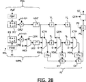
変調器Mは、処理モジュールPMによってデジタル入力信号ISが供給され、述べられた実施例では変調する入力信号ISのタイプに従って8PSK・I/Q変調器M1または線形化GMSK・I/Q変調器M2に供給するように構成される。図2で、M1はMP1とF0とを備え、M2はM20とM21とを備え、M20はMP20とF0(M1と共有される)とを備え、M21はMP21とF1とを備える。 The modulator M is supplied with a digital input signal IS by the processing module PM, and in the embodiment described, an 8PSK I / Q modulator M1 or a linearized GMSK I / Q modulator M2 depending on the type of input signal IS to be modulated. Configured to supply. In FIG. 2, M1 comprises MP1 and F0, M2 comprises M2 0 and M2 1 , M2 0 comprises MP2 0 and F0 (shared with M1), and M2 1 comprises MP2 1 and F1. Is provided.
図2Aおよび2Bに示されるように、線形化GMSK・I/Q変調器M2は好ましくは、線形経路とも呼ばれるゼロ次変調経路M20(MP20およびF0)と、同じ入力信号ISが供給される、直交経路とも呼ばれる少なくとも1次変調経路M21(MP21およびF1)とを備える。線形化GMSK・I/Q変調器M2はより一般的には、同じ入力信号ISが供給されるn+1個の変調経路(n≧0)を備えるn次GMSK・I/Q変調器であることに留意されたい。したがって、変調器Mは、3つ以上の変調経路を備えるGMSK・I/Q変調器を備えてもよい。 As shown in FIGS. 2A and 2B, the linearized GMSK • I / Q modulator M2 is preferably fed with the same input signal IS as the zero-order modulation path M2 0 (MP2 0 and F0), also called the linear path And at least a primary modulation path M2 1 (MP2 1 and F1), also referred to as an orthogonal path. The linearized GMSK • I / Q modulator M2 is more generally an n-order GMSK • I / Q modulator with n + 1 modulation paths (n ≧ 0) supplied with the same input signal IS. Please keep in mind. Therefore, the modulator M may include a GMSK · I / Q modulator including three or more modulation paths.
線形経路は、C0フィルタとも呼ばれるフィルタ部分F0に供給を行なう変調部分MP20を備える。直交経路は、C1フィルタとも呼ばれるフィルタ部分F1に供給を行なう変調部分MP21を備える。 Linear path comprises a modulation part MP2 0 for supplying to the filter portion F0, also called C0 filter. Quadrature path comprises a modulation part MP2 1 for supplying to the filter portion F1, also known as C1 filter.
8PSK・I/Q変調器M1は、C0フィルタF0に供給を行なう変調部分MP1を備え、このC0フィルタF0を、8PSK・I/Q変調器M1が線形化GMSK・I/Q変調器M2の線形経路と共有する。 The 8PSK • I / Q modulator M1 includes a modulation portion MP1 that supplies the C0 filter F0. The 8PSK • I / Q modulator M1 is linearized by the GMSK • I / Q modulator M2 that is linearized. Share with route.
C0フィルタF0およびC1フィルタF1のそれぞれの出力は、主要コンバイナMCに変調されフィルタリングされたI/Q信号を供給するために主要コンバイナMCの入力に接続される。主要コンバイナMCの出力は、デジタル・アナログ変換機DACに変調されフィルタリングされたI/Q信号OSを供給するためにデジタル・アナログ変換機DACにそれ自体が接続された利得制御装置GCに接続される。 The respective outputs of the C0 filter F0 and the C1 filter F1 are connected to the input of the main combiner MC for supplying a modulated and filtered I / Q signal to the main combiner MC. The output of the main combiner MC is connected to a gain controller GC which itself is connected to the digital-to-analog converter DAC to supply a modulated and filtered I / Q signal OS to the digital-to-analog converter DAC. .
8PSK・I/Q変調器M1および線形化GMSK・I/Q変調器M2はそれぞれ、GSMフレームのタイム・スロットに関連する変調されたデジタルI/Q信号を生成するための変調部と、変調されフィルタリングされたデジタルI/Q信号の出力のためフィルタ値によって定義された選択されたパルス形状をデジタルI/Q信号に適用するためのフィルタ部とを備える。 Each of the 8PSK I / Q modulator M1 and the linearized GMSK I / Q modulator M2 is modulated with a modulator for generating a modulated digital I / Q signal associated with a time slot of the GSM frame. And a filter unit for applying the selected pulse shape defined by the filter value to the digital I / Q signal for outputting the filtered digital I / Q signal.
図2Aに概略的にされるように、マルチスロット8PSK・I/Q変調器M1の変調部分MP1は、変調器MのマルチプレクサMUによってシリアル・データ・ストリーム(またはデジタル入力信号)ISが供給される直列並列変換器SPCを備えてもよい。音声信号(しかし、それは純粋なデータであることもある)は音声コーダによって量子化され、次いでチャネル・コーダによってデータ・フレームに編成されてもよいことが思い出されよう。 As schematically illustrated in FIG. 2A, the modulation portion MP1 of the multi-slot 8PSK I / Q modulator M1 is supplied with a serial data stream (or digital input signal) IS by a multiplexer MU of the modulator M. A serial to parallel converter SPC may be provided. It will be recalled that a speech signal (but it may be pure data) may be quantized by a speech coder and then organized into data frames by a channel coder.
たとえば、直列並列変換器SPCは、3ビットの並列信号を出力する、少なくとも3ビット直列並列変換器である。それは好ましくは、4ビットの並列信号を出力する4ビット直列並列変換器であり、ただし、LSB(Least Significant Bit:最下位ビット)が、GMSKデータと8PSKデータの間、ならびに様々なアクティブ(すなわち利得)/再設定/事前ロード・モードの間の区別のために使用される。 For example, the serial-to-parallel converter SPC is at least a 3-bit serial-to-parallel converter that outputs a 3-bit parallel signal. It is preferably a 4-bit serial-to-parallel converter that outputs a 4-bit parallel signal, where LSB (Least Significant Bit) is between GMSK and 8PSK data, as well as various active (ie gain) ) / Reset / preload mode used to distinguish.
マルチスロット8PSK・I/Q変調器M1の変調部MP1は、3ビット並列信号が供給され、また各ビット・トリプレットを8つの複素信号のうちの1つ上にマッピングするように構成されたグレイ・マッパGM(grey mapper)をも備える。 The modulation unit MP1 of the multi-slot 8PSK I / Q modulator M1 is supplied with a 3-bit parallel signal and is configured to map each bit triplet onto one of the 8 complex signals. Mapper GM (grey mapper) is also provided.
マルチスロット8PSK・I/Q変調器M1の変調部分MP1は、グレイ・マッパGMによって出力されたI/Q信号を整形するように構成された複素乗算器CM0をも備える。より厳密には、複素乗算器CM0は、それが受信するk番シンボルを単位円にマッピングする役割を担う。複素乗算器CM0は、3kπ/半径の回転を生じさせるために、受信された各信号に、式(jk3π/8)に等しい回転信号を掛ける。 The modulation portion MP1 of the multi-slot 8PSK I / Q modulator M1 also comprises a complex multiplier CM0 configured to shape the I / Q signal output by the gray mapper GM. More precisely, the complex multiplier CM0 is responsible for mapping the kth symbol received by it to the unit circle. Complex multiplier CM0 multiplies each received signal by a rotation signal equal to equation (jk3π / 8) to produce a rotation of 3 kπ / radius.
シンボル・マッピングは、グレイ・マッパGMによって出力された信号、ならびに式(j3πk/8)の項の追加の回転シンボルを組み合わせる。グレイ・マッパGMは、3ビット・シンボルを、選択された規則に従って単位円上の対応する位置に変換するゲート群と見なされることができる。したがって、乗算器CM0は、RF包絡線上のゼロ交差の回避を可能とする回転されたシンボルを出力している。 Symbol mapping combines the signal output by the gray mapper GM, as well as the additional rotated symbols in the terms of equation (j3πk / 8). The gray mapper GM can be viewed as a group of gates that convert 3-bit symbols into corresponding positions on the unit circle according to selected rules. Thus, the multiplier CM0 outputs a rotated symbol that allows avoiding zero crossings on the RF envelope.
またマルチスロット8PSK・I/Q変調器M1の変調部分MP1は、複素乗算器CM0から供給される第1の入力と、ゼロ設定用の第2の入力と、変調部分MP20の複素乗算器CM1から供給される第3の入力と、各入力サンプルの後にN−1個のゼロを挿入するためのアップサンプリングを実施するように適応されたアップサンプラUS1に入力サンプルを供給する1つの出力とを備える「共有された」3×1マルチプレクサMX1をも備える。たとえば、また図示されるように、N=16である。 The multi-slot modulation part MP1 of 8PSK · I / Q modulator M1 has a first input supplied from the complex multiplier CM0, a second input for zero setting, the complex multiplier CM1 modulation part MP2 0 A third input provided from, and one output for providing input samples to an upsampler US1 adapted to perform upsampling to insert N-1 zeros after each input sample. It also comprises a “shared” 3 × 1 multiplexer MX1. For example, as shown, N = 16.
マルチプレクサMX1の機能は、各保護期間中のゼロと、タイム・スロット(すなわちバーストのアクティブ部分)中の回転された8PSKまたはGPSKシンボルとの間で選択することである。保護期間中にアップサンプラUS1(および後続のC0フィルタF0)にゼロを供給すると、C0フィルタF0の滑らかなステップ・オンおよびステップ・オフ応答が可能となる。 The function of the multiplexer MX1 is to select between zero during each protection period and the rotated 8PSK or GPSK symbol in the time slot (ie the active part of the burst). Supplying zero to upsampler US1 (and subsequent C0 filter F0) during the protection period allows for a smooth step-on and step-off response of C0 filter F0.
このアップサンプラUS1は、共有されたフィルタ部分(すなわちC0フィルタ)F0に、マルチプレクサMX20を介してゼロ、あるいは変調されたデジタル8PSKまたはGMSK・I/Q信号を供給する。 The upsampler US1 is the filter portion (i.e. C0 filter) F0 covalently supplies zero or modulated digital 8PSK or GMSK · I / Q signals through a multiplexer MX2 0.
直列並列変換器SPC、グレイ・マッパGM、乗算器CM0、共有されたマルチプレクサMX1および共有されたアップサンプラUS1は、マルチスロット8PSK・I/Q変調器M1の変調部分MP1を形成する。 The serial-to-parallel converter SPC, the gray mapper GM, the multiplier CM0, the shared multiplexer MX1 and the shared upsampler US1 form the modulation part MP1 of the multislot 8PSK I / Q modulator M1.
C0フィルタF0は、たとえば80タップC0i(i=0からn、ただしn=79)を有するパルス整形フィルタであり、またm=1〜80として、それぞれが80/mフィルタ係数C0iを有する(たとえばm=5の場合、それぞれが16タップを有する5つのセクションがある)m個のセクションF0s(s=1〜m)に分割されてもよい。このC0フィルタF0は、8PSK用に使用され、GMSK変調器のゼロ次部分と共有される。GSMでは、時間帯域幅積がBT=0.3であり、ガウス・パルスが−2T…2Tに制限されるものとして扱われることが思い出されよう。 The C0 filter F0 is, for example, a pulse shaping filter having 80 taps C0 i (i = 0 to n, where n = 79), and m = 1 to 80, each having an 80 / m filter coefficient C0 i ( For example, if m = 5, there may be 5 sections each having 16 taps) and may be divided into m sections F0 s (s = 1-m). This C0 filter F0 is used for 8PSK and is shared with the zero order part of the GMSK modulator. Recall that GSM treats the time-bandwidth product as BT = 0.3 and Gaussian pulses are limited to -2T ... 2T.
C0パルス整形フィルタF0は好ましくは、有限インパルス応答(FIR:finite impulse response)フィルタを定義するロー・パス・フィルタである。こうしたロー・パス・フィルタについては、P. Jungの文献「Laurent's representation of binary digital continuous phase modulated signals with modulation index 1/2 revisited」、IEEE Trans. Comm.、42巻、221〜224頁、1994年に記載されている。
The C0 pulse shaping filter F0 is preferably a low pass filter that defines a finite impulse response (FIR) filter. Such a low-pass filter is described in P. Jung, “Laurent's representation of binary digital continuous phase modulated signals with
C0パルス整形フィルタF0の各部分F0iは、変調されフィルタリングされたデジタルI/Q信号を出力するために、フィルタ値(すなわち係数)C0i(t)によって定義される選択されたパルス形状を、それが受信する変調されたデジタルI/Q信号に適用する。この信号は、すべてのF0iを順次通過する。 Each portion F0 i of the C0 pulse shaping filter F0 has a selected pulse shape defined by the filter value (ie coefficient) C0 i (t) to output a modulated and filtered digital I / Q signal, Applies to the modulated digital I / Q signal it receives. This signal passes through all F0 i sequentially.
C0パルス整形フィルタF0の各フィルタ係数C0iはマルチプレクサMX2iを介して(多分時間遅延された)同じ信号が供給される。より厳密にはフィルタ係数C00はマルチプレクサMX20の出力から供給され、このマルチプレクサMX20はモジュールT1を介して後続のマルチプレクサMX21の3つの入力のうちの1つにも供給を行なう。フィルタ係数C01はマルチプレクサMX21の出力から供給され、このマルチプレクサMX21はモジュールT2を介して後続のマルチプレクサMX22の3つの入力のうちの1つにも供給を行ない、以下同様に続く。最後に、フィルタ係数C0nは、モジュールTnを介してマルチプレクサMX2nの出力から供給される。それぞれのモジュールTi(i=1〜n)は、時間領域内で選択された遅延を生じさせるように構成される。 Each filter coefficient C0 i of the C0 pulse shaping filter F0 is supplied with the same signal (possibly time-delayed) via the multiplexer MX2 i . More precisely filter coefficients C0 0 in is supplied from the output of multiplexer MX2 0, the multiplexer MX2 0 do also supplied to one of the subsequent multiplexer MX2 1 of three inputs via the module T 1. Filter coefficients C0 1 is supplied from the output of multiplexer MX2 1, the multiplexer MX2 1 also performs supplied to one of the subsequent multiplexer MX2 2 three input through the module T 2, less so on. Finally, the filter coefficient C0 n is supplied from the output of the multiplexer MX2 n via the module T n . Each module T i (i = 1-n) is configured to cause a selected delay in the time domain.
図示される実施形態では、C0フィルタF0は、そのn個の各フィルタ係数C0iによってそれぞれ出力された信号を共に組み合わせるためのn−1個のコンバイナ(すなわち加算器)C1からCnをも備える。したがって、C0フィルタF0の最後のコンバイナ(すなわち加算器)Cnの出力は、主要コンバイナMCの2つの入力のうちの1つに接続され、この主要コンバイナMCの出力は、それ自体がデジタル・アナログ変換器DACに接続された利得制御装置GCに接続される。 In the illustrated embodiment, the C0 filter F0 also comprises n-1 combiners (i.e. adders) C1 to Cn for combining together the signals respectively output by their n filter coefficients C0 i . Therefore, the output of the last combiner (ie, adder) Cn of the C0 filter F0 is connected to one of the two inputs of the main combiner MC, and the output of this main combiner MC is itself a digital to analog conversion. Connected to a gain controller GC connected to the DAC.
マルチスロット線形化GMSK・I/Q変調器M2のゼロ次変調経路(MP20およびF0)は、受信された各信号を2つの複素信号のうちの1つの信号にマッピングするように構成されたマッパM0を備える。 The zero order modulation path (MP2 0 and F0) of the multi-slot linearized GMSK • I / Q modulator M2 is a mapper configured to map each received signal to one of two complex signals. M0 is provided.
ゼロ次変調経路は、マッパM0によって出力されたI/Q信号を整形するように構成された複素乗算器CM1をも備える。複素乗算器CM1は、それが受信するシンボルを単位円にマッピングする役割を担う(マッパM0はあり得るアルファベット−1、1を出力し、複素乗算器CM1はアルファベットを、4つの可能な位置のうちの1つを選択する単位円にマッピングする。複素乗算器CM1は、kπ/2半径の回転を生じさせるために、受信された各信号に、式(jkπ/2)に等しい回転信号を掛ける。 The zero order modulation path also includes a complex multiplier CM1 configured to shape the I / Q signal output by the mapper M0. The complex multiplier CM1 is responsible for mapping the symbols it receives to the unit circle (the mapper M0 outputs the possible alphabets -1, 1 and the complex multiplier CM1 converts the alphabet out of the four possible positions. The complex multiplier CM1 multiplies each received signal by a rotation signal equal to equation (jkπ / 2) to produce a rotation of kπ / 2 radius.
乗算器CM1は、上述の共有された3×1マルチプレクサMX1の第3の入力に接続される。 The multiplier CM1 is connected to the third input of the shared 3 × 1 multiplexer MX1 described above.
マッパM0、乗算器CM1、共有されたマルチプレクサMX1および共有されたアップサンプラUS1は、マルチスロットGMSK・I/Q変調器M2の変調部分MP20を構成する。 Mapper M0, multiplier CM1, shared up-sampler US1 multiplexer MX1 and shared was constitute a modulation part MP2 0 multislot GMSK · I / Q modulator M2.
マルチスロット線形化GMSK・I/Q変調器M2の1次(すなわち直交)変調経路(MP21およびF1)は、ゼロ次変調経路(MP20およびF0)のマッパM0と同じデジタルGMSK信号が供給される有限状態マシンFMSを備える。 The first order (ie, quadrature) modulation path (MP2 1 and F1) of the multi-slot linearized GMSK • I / Q modulator M2 is fed with the same digital GMSK signal as the mapper M0 of the zero order modulation path (MP2 0 and F0). A finite state machine FMS.
1次変調経路は、有限状態マシンFSMから来る各信号を2つの複素信号のうちの1つにマッピングするように構成されたマッパM1をも備える。 The primary modulation path also comprises a mapper M1 configured to map each signal coming from the finite state machine FSM to one of two complex signals.
1次変調経路は、マッパM1によって出力されたI/Q信号を整形するように構成された複素乗算器CM2をも備える。複素乗算器CM2は、(k−1)π/2半径の回転を生じさせるために、受信された各信号に、式(j(k−1)π/2)に等しい回転信号を掛ける。 The primary modulation path also includes a complex multiplier CM2 configured to shape the I / Q signal output by the mapper M1. Complex multiplier CM2 multiplies each received signal by a rotation signal equal to equation (j (k-1) π / 2) to produce a rotation of (k-1) π / 2 radius.
1次変調経路は、複素乗算器CM2の出力から供給される1つの入力と、ゼロ設定用の入力と、各入力サンプルの後にN−1個のゼロを挿入するためのアップサンプリングを実施するように適応されたアップサンプラUS2に入力サンプルを供給する1つの出力とを備える2×1マルチプレクサMX3をも備える。たとえば、また図示されるように、N=16である。 The primary modulation path implements one input provided from the output of the complex multiplier CM2, an input for zeroing, and upsampling to insert N-1 zeros after each input sample. And a 2 × 1 multiplexer MX3 with one output for supplying input samples to the upsampler US2 adapted to the above. For example, as shown, N = 16.
マルチプレクサMX3の機能は、各保護期間中のゼロと、タイム・スロット(すなわちバーストのアクティブ部分)の間の回転されたGMSKシンボル(すなわちビット)間で選択することである。 The function of the multiplexer MX3 is to select between zero during each protection period and the rotated GMSK symbols (ie bits) during the time slot (ie the active part of the burst).
有限状態マシンFSMとマッパM1と複素乗算器CMとマルチプレクサMX3とアップサンプラUS2が合わさって、マルチスロット線形化GMSK・I/Q変調器M2の1次変調経路の変調部分MP21を定義している。 The finite state machine FSM, the mapper M1, the complex multiplier CM, the multiplexer MX3, and the upsampler US2 define the modulation part MP2 1 of the primary modulation path of the multi-slot linearized GMSK · I / Q modulator M2. .
アップサンプラUS2は、マルチプレクサMX40を介してフィルタ部分(すなわちC1フィルタ)F1にゼロまたは変調されたデジタルGMSK・I/Q信号を供給する。 Upsampler US2 supplies digital GMSK · I / Q signal zero or modulating the filter portion (i.e. C1 filter) F1 via the multiplexer MX4 0.
C1フィルタF1は、たとえば48タップC1j(J=0〜k、ただしk=47)を有し、それぞれが16個のフィルタ係数C1jを有するp個のセクション(F1p、ただしこの実施例では、p=1〜3)に分割されるパルス整形フィルタである。両方のフィルタF0とF1のフィルタ長は同じ、すなわち80タップ(したがってk=n)でなければならない。しかし、C1フィルタF1の上部の32タップは0であり、したがって、それらは認識される必要はない。適切な時間整合を保証するために、C0フィルタF0とC1フィルタF1の出力間の合計は適切に行なわれなければならないことに留意されたい。 The C1 filter F1 has, for example, 48 taps C1 j (J = 0 to k, where k = 47), and p sections (F1 p , each having 16 filter coefficients C1 j , but in this embodiment, , P = 1 to 3). The filter length of both filters F0 and F1 must be the same, ie 80 taps (and hence k = n). However, the upper 32 taps of the C1 filter F1 are 0, so they do not need to be recognized. Note that the sum between the outputs of the C0 filter F0 and the C1 filter F1 must be done properly to ensure proper time alignment.
C1パルス整形フィルタF1は好ましくは、有限インパルス応答(FIR)フィルタを定義するロー・パス・フィルタである。こうしたロー・パス・フィルタは、上述のP. Jungの文献にも記載されている。 The C1 pulse shaping filter F1 is preferably a low pass filter that defines a finite impulse response (FIR) filter. Such low pass filters are also described in the above-mentioned P. Jung document.
C1パルス整形フィルタF1の各部分F1jは、変調されフィルタリングされたデジタルI/Q信号を出力するために、フィルタ値(すなわち係数)C1j(t)によって定義される、選択されたパルス形状をそれが受信する変調されたデジタルI/Q信号に適用する。 Each portion F1 j of the C1 pulse shaping filter F1 has a selected pulse shape defined by a filter value (ie coefficient) C1 j (t) to output a modulated and filtered digital I / Q signal. Applies to the modulated digital I / Q signal it receives.
C1パルス整形フィルタF1の各係数フィルタC1jは、マルチプレクサMX4jを介して同じ信号(またはその遅延されたバージョン)が供給される。より厳密にはフィルタ係数C10はマルチプレクサMX40の出力から供給され、このマルチプレクサMX40はモジュールT1を介して後続のマルチプレクサMX41の3つの入力のうちの1つにも供給を行なう。フィルタ係数C11はマルチプレクサMX41の出力から供給され、このマルチプレクサMX41はモジュールT2を介して後続のマルチプレクサMX42の3つの入力のうちの1つにも供給を行ない、以下同様に続く。最後に、フィルタ係数C1kは、モジュールTkを介してマルチプレクサMX4kの出力から供給される。 Each coefficient filter C1 j of the C1 pulse shaping filter F1 is supplied with the same signal (or a delayed version thereof) via the multiplexer MX4 j . More precisely the filter coefficient C1 0 is supplied from the output of the multiplexer MX4 0, the multiplexer MX4 0 do also supplied to one of the subsequent multiplexer MX4 1 of three inputs via the module T 1. Filter coefficients C1 1 is supplied from the output of the multiplexer MX4 1, the multiplexer MX4 1 also performs supplied to one of the subsequent multiplexer MX4 2 three input through the module T 2, less so on. Finally, the filter coefficient C1 k is supplied from the output of the multiplexer MX4 k via the module T k .
図示される実施形態では、C0フィルタF1は、そのk個の各フィルタ係数C1jによってそれぞれ出力された信号を共に組み合わせるためのk−1個のコンバイナ(すなわち加算器)C1からCkをも備える。したがって、C1フィルタF1の最後のコンバイナ(すなわち加算器)Ckの出力は、主要コンバイナMCの2つの入力のうちの1つに接続され、この主要コンバイナMCの出力は、それ自体がデジタル・アナログ変換器DACに接続された利得制御装置GCに接続される。 In the illustrated embodiment, C0 filter F1 also comprises a Ck from the k number k-1 one combiner for combining together the signals respectively outputted by each of the filter coefficients C1 j (i.e. adders) C1. Thus, the output of the last combiner (ie, adder) Ck of the C1 filter F1 is connected to one of the two inputs of the main combiner MC, and the output of this main combiner MC is itself a digital to analog conversion. Connected to a gain controller GC connected to the DAC.
図示される実施例では、結合変調器Mは、2つのタイム・スロット間の保護期間の間、すなわち、バーストのアクティブ部分の送信の前(「初期化モード」)および/またはバーストのアクティブ部分の送信の直後(「再設定モード」)、回転された有効シンボルの「ダミー」シーケンスをFIRフィルタ状態にロードする初期化(すなわち事前ロード)手段をも備える。回転されたこれらの有効シンボルは、連続した保護ビットおよびデータ・ビットと時間整合がとられ、保護ビットおよびデータ・ビットは、保護期間、およびその保護期間を囲む連続したタイム・スロットをそれぞれ埋める。 In the illustrated embodiment, the combined modulator M is used during the protection period between two time slots, ie before transmission of the active part of the burst (“initialization mode”) and / or of the active part of the burst. Immediately after transmission (“reset mode”), it also includes initialization (ie, preload) means for loading the “dummy” sequence of rotated valid symbols into the FIR filter state. These rotated valid symbols are time aligned with successive protection bits and data bits, which fill the protection period and successive time slots that surround the protection period, respectively.
より厳密には、初期化操作は、C0 FIRフィルタF0およびC1 FIRフィルタF1((時間領域の遅延のための)モジュールT)内のすべてのフリップ・フロップに有効なシンボルをロードすることを目的とする。有効なシンボルは、GMSKアルファベットからのいずれかの可能なビット組合せであり、適切に回転(および遅延)される。 More precisely, the initialization operation is intended to load a valid symbol on all flip-flops in the C0 FIR filter F0 and the C1 FIR filter F1 (module T (for time domain delay)). To do. A valid symbol is any possible bit combination from the GMSK alphabet and is rotated (and delayed) appropriately.
ダミー・シーケンスの回転は、位相ジャンプなしにダミー・シーケンスとデータ・ビットの間の切換えを可能にする。事実上、80タップを有するフィルタ(F0、F1)においては、入力信号は出力において見える前に、まずフィルタを通過しなければならない。したがって、回転された有効シンボルの有効ダミー・シーケンスは、それが電力−時間テンプレートに適合している限り何でも送信することが可能である場合、保護期間の間にFIRフィルタ内にロードされなければならない。 The rotation of the dummy sequence allows switching between the dummy sequence and the data bits without phase jumps. In effect, in a filter with 80 taps (F0, F1), the input signal must first pass through the filter before it can be seen at the output. Thus, a valid dummy sequence of rotated valid symbols must be loaded into the FIR filter during the protection period if it can transmit anything as long as it fits the power-time template. .
この種類の初期化を用いて、(保護期間の間、送信が行なわれないことによる)非常に小さい振幅から、必要とされる振幅レベルへの急な遷移を得ることができる。 With this type of initialization, it is possible to obtain a sharp transition from a very small amplitude (due to no transmission during the protection period) to the required amplitude level.
初期化(すなわち事前ロード)手段は2つの部分に分けられてもよい。少なくとも線形化GMSK・I/Q変調器M2のゼロ次経路(MP20およびF0)に、また多分(図2Aに示されるような)マルチスロット8PSK・I/Q変調器M1に専用の第1の部分MIa、および(図2Bに示されるような)線形化GMSK・I/Q変調器M2のマルチスロット1次経路(MP21およびF1)に専用の第2の部分MIb。 The initialization (ie preloading) means may be divided into two parts. A first dedicated to at least the zero-order path (MP2 0 and F 0 ) of the linearized GMSK · I / Q modulator M2 and possibly to the multislot 8PSK · I / Q modulator M1 (as shown in FIG. 2A). Part MIa and a second part MIb dedicated to the multi-slot primary path (MP2 1 and F1) of the linearized GMSK • I / Q modulator M2 (as shown in FIG. 2B).
図2Aに示される実施例では、初期化(すなわち事前ロード)手段の第1の部分MIaは、マルチスロット8PSK・I/Q変調器M1に専用の(GMSK切換えだけが使用される場合は必須でない)下位部分MIOと、線形化GMSK・I/Q変調器M2のゼロ次経路(MP20およびF0)に専用の第2の部分MI1とを備える。 In the embodiment shown in FIG. 2A, the first part of the initialization (ie preload) means MIa is not mandatory if the multislot 8PSK I / Q modulator M1 is dedicated (if only GMSK switching is used) ) comprises a lower portion MIO, and a second portion MI1 dedicated zero order path linearized GMSK · I / Q modulator M2 (MP2 0 and F0).
第1の下位部分MI0は、選択された初期化(すなわち事前ロード)シーケンス・ビットPLSが供給される直列並列変換器SPC’を備える。直列並列変換器SPCとして、この直列並列変換器SPC’は、たとえば、3ビットの並列信号PLSを出力する3ビット直列並列変換器である。 The first lower part MI0 comprises a serial to parallel converter SPC 'which is supplied with a selected initialization (ie preload) sequence bit PLS. As the serial-parallel converter SPC, the serial-parallel converter SPC 'is, for example, a 3-bit serial-parallel converter that outputs a 3-bit parallel signal PLS.
第1の下位部分MI0は3ビットの並列信号が供給され、また各ビット・トリプレットを8つの複素信号のうちの1つにマッピングするように構成されたグレイ・マッパGM’をも備える。 The first sub-portion MI0 is provided with a 3-bit parallel signal and also comprises a gray mapper GM 'configured to map each bit triplet to one of eight complex signals.
第1の下位部分MI0は、グレイ・マッパGM’によって出力された信号を整形するように構成された複素乗算器CM0’をも備える。複素乗算器CM0’は、3kπ/8半径の回転を生じさせるために、受信された各信号に、式(jk3π/8)に等しい回転信号を掛ける。したがって、複素乗算器CM0’は、事前ロード、再設定およびアクティブ・モード間で切り換えるときにその信号を入力データと適切に位相合わせすることを可能とする回転されたシンボルを出力する。 The first lower part MI0 also comprises a complex multiplier CM0 'configured to shape the signal output by the gray mapper GM'. The complex multiplier CM0 'multiplies each received signal by a rotation signal equal to equation (jk3π / 8) to produce a rotation of 3kπ / 8 radius. Thus, complex multiplier CM0 'outputs a rotated symbol that allows the signal to be properly phased with the input data when switching between preload, reset and active modes.
代替法では、すべてのビットがゼロ(0)または一(1)に等しい入力シーケンスを生成することが可能である。このため、複素乗算器CM0’の入力をマイナス一(−1)または一(1)に配線することが可能であり、したがって直列並列変換器SPC’が、またグレイ・マッパ(または8PSK初期化切換えが予見されない場合には分岐全体さえ)もが省かれる。 Alternatively, it is possible to generate an input sequence in which all bits are equal to zero (0) or one (1). For this reason, it is possible to wire the input of the complex multiplier CM0 ′ to minus one (−1) or one (1), so that the serial-to-parallel converter SPC ′ is also connected to the gray mapper (or 8PSK initialization switch). If this is not foreseen, the entire branch) will be omitted.
第2の下位部分MI1は、選択された初期化(すなわち事前ロード)シーケンス・ビットPLS’が供給され、またマッパM0として各ビットを2つの複素信号のうちの1つにマッピングするように構成されたマッパM0’を備える。 The second sub-portion MI1 is provided with a selected initialization (ie preload) sequence bit PLS ′ and is configured as a mapper M0 to map each bit to one of two complex signals. Mapper M0 ′.
第2の下位部分MI1は、マッパM0’によって出力された信号を整形するように構成された複素乗算器CM1’をも備える。複素乗算器CM1’は、kπ/2半径の回転を生じさせるために、受信された各信号に、式(jkπ/2)に等しい回転信号を掛ける。したがって、複素乗算器CM1’は、事前ロード、再設定およびアクティブ・モード間で切り換えるときにその信号を入力データと適切に位相合わせすることを可能とする回転されたシンボルを出力する。 The second lower part MI1 also comprises a complex multiplier CM1 'configured to shape the signal output by the mapper M0'. The complex multiplier CM1 'multiplies each received signal by a rotation signal equal to equation (jkπ / 2) to produce a rotation of kπ / 2 radius. Thus, complex multiplier CM1 'outputs a rotated symbol that allows the signal to be properly phased with the input data when switching between preload, reset and active modes.
代替法では、すべてのビットがゼロ(0)または一(1)に等しい入力シーケンスを生成することが可能である。このため、複素乗算器CM1’の入力をマイナス一(−1)または一(1)に配線することが可能であり、したがってマッパM0’が省かれる。 Alternatively, it is possible to generate an input sequence in which all bits are equal to zero (0) or one (1). For this reason, it is possible to wire the input of the complex multiplier CM1 'to minus one (-1) or one (1), and thus the mapper M0' is omitted.
初期化手段の第1の部分MIaもまた、複素乗算器CM0’の出力から供給される第1の入力と、複素乗算器CM1’から供給される第2の入力と、初期化(すなわち事前ロード)モードのため選択された有効回転ビットを出力するため各入力サンプルの後にN−1個のゼロを挿入するためのアップサンプリングを実施するように適応されたアップサンプラUS1’に入力サンプルを供給する1つの出力とを備えた、共有された2×1マルチプレクサMX0を備える。図示される実施例では、N=16である。 The first part MIa of the initialization means also includes a first input supplied from the output of the complex multiplier CM0 ′, a second input supplied from the complex multiplier CM1 ′, and initialization (ie preloading). ) Supply input samples to upsampler US1 ′ adapted to perform upsampling to insert N−1 zeros after each input sample to output the effective rotation bit selected for the mode With a shared 2 × 1 multiplexer MX0 with one output. In the illustrated embodiment, N = 16.
マルチプレクサMX0の機能は、事前ロードまたは再設定モードの間(それが実装される場合、すなわち8PSK経路の初期化が予見される場合)、回転された8PSKとGPSKシンボル間で選択することである。 The function of the multiplexer MX0 is to select between the rotated 8PSK and GPSK symbols during the preload or reset mode (if it is implemented, i.e. if the initialization of the 8PSK path is foreseen).
アップサンプラUS1’の出力は、マルチプレクサMX20の第1の入力に、またそれぞれモジュールT’1からT’k(時間領域遅延のモジュール)を介して他の各マルチプレクサMX21からMX2kの第1の各入力に接続される。 The output of the upsampler US1 ′ is connected to the first input of the multiplexer MX2 0 and to the first of each of the other multiplexers MX2 1 to MX2 k via modules T ′ 1 to T ′ k (modules of time domain delay), respectively. Connected to each input.
したがって各マルチプレクサMX2iの第1の入力には初期化(すなわち事前ロード)モードのための回転された信号が供給され、各マルチプレクサMX2iの第2の入力にはアクティブ・モードのための回転された信号が供給され、各マルチプレクサMX2iの第3の入力には再設定モードのためのゼロ・シーケンスが供給される。 Accordingly rotated signals for initialization (i.e. preload) mode is supplied to the first input of each multiplexer MX2 i, is rotated for the active mode to the second input of each multiplexer MX2 i The third input of each multiplexer MX2 i is supplied with a zero sequence for the reset mode.
初期化(すなわち事前ロード)手段の第2の部分MIbは、マッパM0’と同じ選択された初期化(すなわち事前ロード)ビット・シーケンスPLS’が好ましくは供給される有限状態マシンFSMを備える。 The second part MIb of the initialization (ie preload) means comprises a finite state machine FSM which is preferably supplied with the same selected initialization (ie preload) bit sequence PLS 'as the mapper M0'.
第2の部分MIbは、有限状態マシンFSM’から来る各信号を2つの複素信号のうちの1つにマッピングするように構成されたマッパM1’をも備える。 The second part MIb also comprises a mapper M1 'configured to map each signal coming from the finite state machine FSM' to one of two complex signals.
第2の部分MIbは、マッパM1’から出力された信号を整形するように構成された複素乗算器CM2’をも備える。複素乗算器CM2’は、(k−1)π/2半径の回転を生じさせるために、受信された各信号に、式(j(k−1)π/2)に等しい回転信号を掛ける。したがって、複素乗算器CM2’は、アクティブ、事前ロードおよび再設定モード間で切り換えるときにその信号を適切に位相合わせすることを可能とする回転されたシンボルを出力する。 The second part MIb also comprises a complex multiplier CM2 'configured to shape the signal output from the mapper M1'. Complex multiplier CM2 'multiplies each received signal by a rotation signal equal to equation (j (k-1) π / 2) to produce a rotation of (k-1) π / 2 radius. Thus, complex multiplier CM2 'outputs a rotated symbol that allows the signal to be properly phased when switching between active, preload and reset modes.
第2の部分MIbは、回転されたシンボル・サンプルが乗算器CM2’の出力から供給され、また初期化(すなわち事前ロード)モードのため選択された有効回転ビットを出力するため各サンプルの後にN−1個のゼロを挿入するためのアップサンプリングを実施するように構成されたアップサンプラUS2’をも備える。図示される実施例では、N=16である。 The second part MIb is supplied with the rotated symbol samples from the output of the multiplier CM2 ′ and N after each sample to output the effective rotation bits selected for the initialization (ie preload) mode. It also comprises an upsampler US2 ′ configured to perform upsampling to insert −1 zeros. In the illustrated embodiment, N = 16.
アップサンプラUS2’の出力は、マルチプレクサMX40の第1の入力に、またそれぞれモジュールT’1からT’k(時間領域遅延のモジュール)を介して他の各マルチプレクサMX41からMX4kの第1の各入力に接続される。
Upsampler US2 the 'output of, to a first input of multiplexer MX4 0, also the module T' respectively from each multiplexer MX4 1 other via a T 'k from 1 (module time domain delay) of
したがって、各マルチプレクサMX4jの第1の入力には初期化(すなわち事前ロード)モードのための回転された信号が供給され、各マルチプレクサMX4jの第2の入力にはアクティブ・モードのための回転された信号が供給され、各マルチプレクサMX4jの第3の入力には再設定モードのためのゼロ・シーケンスが供給される。 Thus, the rotation signal for the first initialization input of each multiplexer MX4 j (i.e. preload) mode is supplied, the rotation for the active mode to the second input of each multiplexer MX4 j And the third input of each multiplexer MX4 j is supplied with a zero sequence for the reset mode.
代替法では、すべてのビットがゼロ(0)または一(1)に等しい入力シーケンスを生成することが可能である。このため、複素乗算器CM2’の入力をマイナス一(−1)または一(1)に配線することが可能であり、したがってマッパM2’および有限状態マシンFSM’が省かれる。 Alternatively, it is possible to generate an input sequence in which all bits are equal to zero (0) or one (1). For this reason, it is possible to wire the input of the complex multiplier CM2 'to minus one (-1) or one (1), thus eliminating the mapper M2' and the finite state machine FSM '.
複素乗算器CM1およびCM2は、選択された定数値およびそれぞれ式(jkπ/2)および式(j(k−1)π/2)項が供給される追加の入力を備えてもよく、それによってマッパMOおよびM1の省略がもたらされることに留意されよう。これは、初期化(すなわち事前ロード)が、有効な適切に回転されたシンボルだけを用いて行なわれる必要があるので可能である。このため、追加の入力を1(または−1)に配線することが可能であり、CMiにより依然として回転させることによって、アクティブ・モードと位相合わせされ、すなわち位相ジャンプを生じさせずに切り換えられ得る適切に回転されたダミー・シーケンスがもたらされる。この場合、それがあらゆる定数入力について同じ出力を計算するので、有限状態マシンFSM(ほぼモジュロ2加算器の働きをする)を省くことも可能である。 The complex multipliers CM1 and CM2 may comprise additional inputs supplied with the selected constant values and the terms (jkπ / 2) and (j (k−1) π / 2) respectively. Note that the omission of mappers MO and M1 results. This is possible because initialization (ie preloading) needs to be done with only valid properly rotated symbols. For this reason, it is possible to wire an additional input to 1 (or -1) and it can be phased with active mode by still rotating with CMi, i.e. can be switched without causing a phase jump. A rotated dummy sequence is provided. In this case, it is possible to omit the finite state machine FSM (which acts almost as a modulo-2 adder) because it calculates the same output for every constant input.
結合変調器Mは、バーストのアクティブ部分の送信直後および保護期間の間に、FIRフィルタ状態にすべてゼロのシーケンス(係数C0(i)およびC1(j))をロードする再設定手段をも備えてもよい。選択されたこのすべてゼロのシーケンスは、FIRフィルタ状態が(送信振幅を伴う)最後の有効シンボルから、非常に小さい振幅に対応する保護期間のすべてゼロの状態に高速に遷移することを得るために供給される。FIRフィルタを通過するゼロ・シーケンスは、フィルタの出力での滑らかなステップ・オン/ステップ・オフとして現れる。 The combined modulator M also comprises resetting means for loading the FIR filter state with a sequence of all zeros (coefficients C0 (i) and C1 (j)) immediately after transmission of the active part of the burst and during the protection period. Also good. This selected all-zero sequence is to obtain that the FIR filter state quickly transitions from the last valid symbol (with transmit amplitude) to the all-zero state of the protection period corresponding to a very small amplitude. Supplied. The zero sequence that passes through the FIR filter appears as a smooth step on / step off at the output of the filter.
こうしたすべてゼロのシーケンスは、それが初期化手段(この場合には初期化手段は再設定手段としても働く)によって生成される場合、各マルチプレクサMX2iまたはMX4jの第3の入力を介して、そうでなければ各マルチプレクサMX2iまたはMX4jの第1の入力(事前ロード(または初期化)信号に専用)を介して取り入れられてもよい。 Such an all-zero sequence is generated via the third input of each multiplexer MX2 i or MX4 j if it is generated by an initialization means (in which case the initialization means also serves as a resetting means) Otherwise, it may be taken in via the first input of each multiplexer MX2 i or MX4 j (dedicated to the preload (or initialization) signal).
上述したように、オン/オフ状態(データ・モード対初期化モード)の間の遷移が瞬間的であるように、変調切換えならびに利得変更は、正確にタイミングがとられなければならない。 As described above, modulation switching as well as gain changes must be accurately timed so that the transition between on / off states (data mode versus initialization mode) is instantaneous.
このため、本発明による制御デバイスCDは専用メモリMM1を備え、この専用メモリMM1内では、ベースバンドおよびオーディオ・インターフェース・デバイスBAI用のシンボルとデジタル・インターフェースIを介した無線周波数デバイスRFDへの送信のための符号化値の間の対応を確立する符号化テーブルが格納される。 For this purpose, the control device CD according to the invention comprises a dedicated memory MM1, in which the symbols for baseband and audio interface device BAI and transmission to the radio frequency device RFD via the digital interface I A coding table is stored that establishes a correspondence between coded values for.
より厳密には、この符号化テーブルは、変調器M(M1、M20およびM21)に供給するためのデータ・ワードを備える第1群のシンボル(たとえば少なくとも8個、好ましくは10個(8PSKのための8個、GMSKのための2個)と、変調器Mおよび/または利得制御装置GCの動作を制御するためのコマンド・ワードを備える(たとえば少なくとも6個の)第2のシンボル群とを備える。 More precisely, this coding table comprises a first group of symbols (eg at least 8 and preferably 10 (8PSK) comprising data words for feeding to the modulator M (M1, M2 0 and M2 1 ). 8 for GMSK and 2 for GMSK) and a second symbol group (eg, at least 6) comprising command words for controlling the operation of modulator M and / or gain controller GC Is provided.
こうした符号化テーブルは、ベースバンド・デバイスBBD内で生成されたシンボルをデジタル・インターフェースIを介してベースバンドおよびオーディオ・インターフェース・デバイスBAIに送信されるように適応された特定の符号化された値(すなわち送信シンボル・ビット)に変換することを可能にする。 These encoding tables are specific encoded values adapted to transmit symbols generated in the baseband device BBD via the digital interface I to the baseband and audio interface device BAI. (Ie transmitted symbol bits).
ベースバンド・デバイスBBDは、ベースバンドおよびオーディオ・インターフェース・デバイスBAIにデータまたは1つまたは複数のコマンドを送信する必要がある場合、それ(またはそれら)を制御デバイスCDに送信する。次いで、制御デバイスCDは制御モジュールCRMにデータまたは1つまたは複数のコマンドを送信し、この制御モジュールCRMは、制御デバイスCDが備えており、送信するデータ、または1つまたは複数のコマンドに対応する符号化された値をその符号化テーブル内で決定するために専用メモリMMIにアクセスするように構成される。次いで、制御モジュールCRMは、この符号化された値がベースバンドおよびオーディオ・インターフェース・デバイスBAIに送信され得るように、それをベースバンド・デバイスBBDに送信する。 If the baseband device BBD needs to send data or one or more commands to the baseband and audio interface device BAI, it sends it (or them) to the control device CD. The control device CD then sends data or one or more commands to the control module CRM, which is provided in the control device CD and corresponds to the data to be sent or one or more commands. It is configured to access the dedicated memory MMI to determine the encoded value in its encoding table. The control module CRM then sends it to the baseband device BBD so that this encoded value can be sent to the baseband and audio interface device BAI.
図示される実施例では、制御装置CD全体(制御モジュールCRMおよび専用メモリMM1)がベースバンド・デバイスBBD内に置かれているが、これは、これは必須ではない。確かに、制御装置CDの一部、特に専用メモリMM1は、ベースバンド・デバイスBBDの外部に置かれてもよい。 In the illustrated embodiment, the entire controller CD (control module CRM and dedicated memory MM1) is located in the baseband device BBD, but this is not essential. Certainly, part of the control device CD, in particular the dedicated memory MM1, may be located outside the baseband device BBD.
符号化テーブルはソフトウェアまたはファームウェアとして実装されてもよいが、それは、デジタル・インターフェースI上で実行されるプロトコル・スタックであることもある。 The encoding table may be implemented as software or firmware, but it may be a protocol stack that runs on the digital interface I.
ベースバンドおよびオーディオ・インターフェース・デバイスBAIの処理モジュールPMは、符号化テーブルの符号化値と、変調器Mおよび/または利得制御装置GCの動作を制御するためのコマンド・ワードを表すシンボル、ならびに変調器Mに供給するためのデータ・ワードとの間の対応を確立する制御テーブルを格納する専用メモリMM2と、メモリMM2、符号化テーブルを用いて符号化された送信シンボル・ビットを受信するためデジタル・インターフェースIに、また変調器M(より厳密にはマルチプレクサMX1、MX2i、MX3およびMX4j、また予見される場合にはMX0にも)および利得制御装置GCに接続された制御モジュールCTMとを備える。 The processing module PM of the baseband and audio interface device BAI has a coding value of the coding table, a symbol representing a command word for controlling the operation of the modulator M and / or the gain controller GC, and the modulation A dedicated memory MM2 for storing a control table that establishes a correspondence between data words to be supplied to the device M, a memory MM2, a digital signal for receiving transmission symbol bits encoded using the encoding table A control module CTM connected to the interface I and also to the modulator M (more precisely multiplexers MX1, MX2 i , MX3 and MX4 j and also MX0 if foreseen) and the gain controller GC Prepare.
制御モジュールCTMは、デジタル・インターフェースIから符号化された値、すなわち符号化テーブルで符号化された送信シンボル・ビットを受信するとき、専用メモリMM2にアクセスして、その制御テーブル内で、受信された符号化値に対応するワードを決定する。次いで、それは、このワードを変調器Mおよび/または利得制御装置GCに送信する。 When the control module CTM receives the encoded value from the digital interface I, i.e. the transmission symbol bits encoded in the encoding table, it accesses the dedicated memory MM2 and receives it in that control table. The word corresponding to the encoded value is determined. It then sends this word to the modulator M and / or the gain controller GC.
図示される実施例では、制御モジュールCTMおよび専用メモリMM2は、ベースバンドおよびオーディオ・インターフェース・デバイスBAI内に置かれているが、これは必須ではない。確かに、少なくとも専用メモリMM2は、ベースバンドおよびオーディオ・インターフェース・デバイスBAIの外部に置かれてもよい。 In the illustrated embodiment, the control module CTM and dedicated memory MM2 are located in the baseband and audio interface device BAI, but this is not required. Indeed, at least the dedicated memory MM2 may be placed outside the baseband and audio interface device BAI.
制御テーブルは、ソフトウェアまたはファームウェアとして実装されてもよいが、それは、デジタル・インターフェースI上で実行されるプロトコル・スタックとすることもできる。プロトコル・スタックを含む変調器全体は、ファームウェアでも実装され得る。 The control table may be implemented as software or firmware, but it can also be a protocol stack running on the digital interface I. The entire modulator, including the protocol stack, can also be implemented in firmware.
第2群のシンボルは、変調器Mおよび/または利得制御装置GCの動作を制御するように構成されたあらゆるタイプのコマンドを定義するために使用されてもよい。 The second group of symbols may be used to define any type of command configured to control the operation of modulator M and / or gain controller GC.
たとえば、コマンド・ワードが、選択された利得値を利得制御装置GCに割り当てるため、または選択された動作モードをC0フィルタF0(マルチプレクサMX2i)および/またはC1フィルタF1(マルチプレクサMX4j)、および/または変調部分MIa(マルチプレクサMX0およびMX1)および/またはMIb(マルチプレクサMX3)に割り当てるために提供されてもよい。 For example, the command word assigns the selected gain value to the gain controller GC, or the selected operating mode is C0 filter F0 (multiplexer MX2 i ) and / or C1 filter F1 (multiplexer MX4 j ), and / or Or it may be provided for assignment to the modulation part MIa (multiplexers MX0 and MX1) and / or MIb (multiplexer MX3).
コマンド・ワードもまた、選択された動作モードをC0フィルタF0(マルチプレクサMX2i)および/またはC1フィルタF1(マルチプレクサMX4j)、および/または変調部分MIa(マルチプレクサMX0およびMX1)および/またはMIb(マルチプレクサMX3)に割り当てるため、また選択された利得値を利得制御装置GCに割り当てるためにも提供されてもよい。 The command word also selects the selected mode of operation as C0 filter F0 (multiplexer MX2 i ) and / or C1 filter F1 (multiplexer MX4 j ), and / or modulation portion MIa (multiplexers MX0 and MX1) and / or MIb (multiplexer). MX3) and may be provided for assigning the selected gain value to the gain controller GC.
ここでは、「動作モード」は、変調器Mの即時の立上げのために、回転された有効なシンボルの選択されたシーケンスをフィルタF0および/またはF1に事前ロードするために使用される上述の初期化モード、または変調器Mの即時の立下げのために変調器Mのすべての遅延にゼロの2進値を強制的に入れ、そうでない場合は変調器のアルファベットからの有効データ・シンボルの送信を強制するために使用される上述の再設定モードを意味する。 Here, the “operation mode” is used to preload the selected sequence of rotated valid symbols into the filters F0 and / or F1 for the immediate start-up of the modulator M. Force a binary value of zero into all delays of the modulator M for initialization mode, or for immediate fall of the modulator M, otherwise of valid data symbols from the modulator alphabet It means the above-mentioned reset mode used to force transmission.
しかし、他の動作モードが考えられてもよい。 However, other operating modes may be considered.
変調器Mまたは利得制御装置GCは、制御モジュールCTMからワードを受信すると、関係する要素(マルチプレクサおよび/または直列並列変換機および/またはマッパおよび/または有限状態マシンおよび/または利得乗算器)が対応する動作を適切な瞬間に実施することができるように、それにワードを送信する。 When the modulator M or the gain controller GC receives a word from the control module CTM, the relevant elements (multiplexer and / or serial-to-parallel converter and / or mapper and / or finite state machine and / or gain multiplier) are supported. Send the word to it so that the action to be performed can be performed at the appropriate moment.
変調器MがGMSK・I/Q変調器M20およびM21と、8PSK・I/Q変調器M1とを備える場合、符号化テーブルおよび制御テーブルは好ましくは、上述の文献「DigRF, Baseband / RF digital interface specification : Logical, Electrical and timing characteristics」、第1.12版で定義されたタイプのものである。 A modulator M is GMSK · I / Q modulator M2 0 and M2 1, if and a 8PSK · I / Q modulator M1, encoding table and the control table are preferably the above literature "DigRF, Baseband / RF digital interface specification: Logical, Electrical and timing characteristics ", version 1.12.
より厳密には、digRF規格に準拠した符号化された各値は、3つの最上位ビット(MSB)と1つの下位ビット(LSB)とを備える4ビットのワードである。LSBは、GMSK・I/Q変調器M20およびM21を、8PSK・I/Q変調器M1と区別するために使用される。MSBがまず送信される。 More precisely, each encoded value according to the digRF standard is a 4-bit word with three most significant bits (MSB) and one least significant bit (LSB). The LSB is used to distinguish the GMSK • I / Q modulators M2 0 and M2 1 from the 8PSK • I / Q modulator M1. The MSB is transmitted first.
さらに、またやはりdigRF規格によれば、第1のシンボル群は、それぞれが互いに異なるデータに専用である10個のシンボルを備え、第2のシンボル群は、互いに異なるコマンドの専用である6個のシンボルを備える。 Furthermore, also according to the digRF standard, the first symbol group comprises 10 symbols, each dedicated to different data, and the second symbol group consists of 6 different commands dedicated to different commands. With symbols.
符号化テーブルの一例が以下に示されている(制御テーブルは、入出力を反転させることによって、この符号化テーブルから容易に推論され得る)。

格納された符号化テーブルまたは制御テーブルは、16進値と2進値の両方を備える必要はないことに留意されたい。 Note that the stored encoding table or control table need not comprise both hexadecimal and binary values.
このテーブルでは、最初の2つのシンボルは、GMSK・I/Q変調器M20およびM21のための2つの異なるデータ・ワードに専用であり、6つの後続のシンボルは、最初は独自の使用に専用であり、最後は6つの変調器M(マルチプレクサ構成)および/または利得制御装置GC(利得変更)コマンドに割り当てられ、最後の8つのシンボルは、8PSK・I/Q変調器M1のための8つの異なるデータ・ワードに専用である。 In this table, the first two symbols are dedicated to two different data words for the GMSK I / Q modulators M2 0 and M2 1 , and the six subsequent symbols are initially for their own use. Dedicated, last assigned to 6 modulators M (multiplexer configuration) and / or gain controller GC (gain change) command, the last 8 symbols are 8 for 8PSK I / Q modulator M1 Dedicated to two different data words.
符号化された値の他の形式が考えられてもよい。 Other forms of the encoded value may be envisaged.
本発明によれば、独自のビットを使用して、i)デジタル乗算器またはアナログ・スケーリング回路を用いて利得を変更し、ii)通常のI/Qパルス整形フィルタのステップ・オンのためにFIRフィルタ(F0およびF1)を事前ロードし、iii)通常のI/Qパルス整形フィルタのステップ・オフのためにFIRフィルタを再設定し、iv)利得変更を事前ロード、再設定または強制ゼロ入力と組み合わせることが現在可能である。 In accordance with the present invention, a unique bit is used to i) change gain using a digital multiplier or analog scaling circuit, and ii) FIR for step-on of a normal I / Q pulse shaping filter. Preload the filters (F0 and F1), iii) reset the FIR filter for normal I / Q pulse shaping filter step-off, and iv) preload, reset or force zero input with gain change Combinations are now possible.
コマンド・ワード(独自のビット)の使用は、対応する動作を適切な瞬間に実施し得るように、各コマンド・ワードが変調器Mおよび/または利得制御装置GCに送信されなければならない厳密な時を定義する適切なタイミング図なしでは「無意味」である。 The use of command words (proprietary bits) is a precise time when each command word must be sent to the modulator M and / or the gain controller GC so that the corresponding operation can be performed at the appropriate moment. Without a proper timing diagram to define
線形化GMSK・I/Q変調器M2について、より厳密にはそのマルチプレクサMX1およびMX3(上部)およびそのマルチプレクサMX2およびMX4(下部)についてのタイミング図の非限定的な例が、図3に示されている。 A non-limiting example of a timing diagram for the linearized GMSK I / Q modulator M2, more precisely its multiplexers MX1 and MX3 (top) and its multiplexers MX2 and MX4 (bottom) is shown in FIG. ing.
ここでは、事前ロード(すなわち初期化)は、G1からG4で参照される4つの先行保護ビットの後に行なわれ、これらの先行保護ビットの後に、特別に定義された他の保護ビットG5からG7が続く。これらの保護ビットは、データ・ビットで埋められた連続した2つのタイム・スロット間に挿入された保護期間を埋めている。 Here, preloading (ie initialization) takes place after the four pre-protection bits referenced by G1 to G4, after which the other specially defined protection bits G5 to G7 Continue. These guard bits fill the guard period inserted between two consecutive time slots filled with data bits.
より厳密には、この実施例では保護期間はG1、…、G7(保護ビット)を要するが、変調器M2はG4の後にだけオンにされる。したがって、G1、G2およびG3の間、マルチプレクサMX1およびMX3は、強制のゼロに設定され(第2入力オン)、マルチプレクサMX2およびMX4はアクティブに設定される(第2入力オン)。したがって、前のGMSKバーストからの滑らかなステップ・ダウンが得られる。G4で、マルチプレクサMX1およびMX3はGMSK2に切り換えられ(第1入力オン)、マルチプレクサMX2およびMX4は、ダミー・シーケンスのC0またはC1フィルタへの事前ロードを可能にするため事前ロードに設定される(第1入力オン)。したがって、高速振幅遷移は出力で生じ、新しいデータ・ビットがダミー・シーケンスの後に続き、「実際のデータ」が2.5シンボル後に出力に到達する。 More precisely, in this embodiment, the protection period requires G1,..., G7 (protection bits), but the modulator M2 is turned on only after G4. Thus, during G1, G2 and G3, multiplexers MX1 and MX3 are set to forced zero (second input on) and multiplexers MX2 and MX4 are set active (second input on). Thus, a smooth step down from the previous GMSK burst is obtained. At G4, multiplexers MX1 and MX3 are switched to GMSK2 (first input on) and multiplexers MX2 and MX4 are set to preload to allow preloading of the dummy sequence to the C0 or C1 filter (first). 1 input on). Thus, fast amplitude transitions occur at the output, with new data bits following the dummy sequence and “actual data” reaching the output after 2.5 symbols.
図3で、末尾ビットT0およびT2の後にはデータ・ビット(図示されておらず、「通常の」遷移に対応する)が続き、このデータ・ビットの後には他の末尾ビットT’0からT’2が続いており、t/Tビットは「正規化された時間尺度」を表す。 In FIG. 3, the tail bits T0 and T2 are followed by data bits (not shown, corresponding to “normal” transitions) followed by the other tail bits T′0 to T Followed by '2 and the t / T bit represents a "normalized time scale".
この実施例では、再設定部分(強制のゼロ)は、第3の後続保護ビットG’3、すなわちバーストのアクティブ・モードの後、また特別に定義されたさらなる3つの保護ビット(G’0からG’2)の追加の送信の後に続く。再設定モードはG’0の間に既にアクティブ化され得るが、実際には、スイッチ・オフ・プロセスのためにいくらかの時間を取り入れることが好ましい。 In this embodiment, the reset part (forced zero) is the third subsequent protection bit G′3, ie after the active mode of the burst, and three more specially defined protection bits (from G′0). Following an additional transmission of G′2). The reset mode can already be activated during G'0, but in practice it is preferable to take some time for the switch-off process.
図3の上部のグレイ・シンボルは、いずれか1つが選択され得ることを示している。 The gray symbol at the top of FIG. 3 indicates that any one can be selected.
この実施例では、変調器のマルチプレクサ上の動作だけが予見されているが、再設定ならびに事前ロードは、利得制御装置GC内の利得変更と組み合わされてもよい。 In this embodiment, only operation on the modulator multiplexer is foreseen, but resetting and preloading may be combined with gain changes in the gain controller GC.
本発明は、単に例として上述されている制御デバイス、ベースバンド・デバイス、ベースバンド(およびオーディオ)インターフェース・デバイス、および無線通信機器に限定されないが、それは、特許請求の範囲内で当業者によって考慮されてもよいすべての代替実施形態を包含するものである。 The present invention is not limited to the control devices, baseband devices, baseband (and audio) interface devices, and wireless communication equipment described above by way of example only, but is contemplated by those skilled in the art within the scope of the claims. It encompasses all alternative embodiments that may be made.
したがって、上記の説明では、それは集積回路として実装された変調器について述べられているが、本発明は、すべての値が事前に計算され格納される純粋なルックアップ・テーブルとして、そうでない場合は純粋なファームウェアとして実装される変調器にも適用される。 Thus, in the above description, it is described for a modulator implemented as an integrated circuit, but the present invention is a pure lookup table where all values are pre-calculated and stored, otherwise It also applies to modulators implemented as pure firmware.
Claims (16)
Applications Claiming Priority (3)
| Application Number | Priority Date | Filing Date | Title |
|---|---|---|---|
| EP04300496 | 2004-07-29 | ||
| EP04300496.9 | 2004-07-29 | ||
| PCT/IB2005/052312 WO2006013484A1 (en) | 2004-07-29 | 2005-07-12 | Enhanced bit mapping for digital interface of a wireless communication equipment in multi-time slot and multi-mode operation |
Publications (2)
| Publication Number | Publication Date |
|---|---|
| JP2008508765A JP2008508765A (en) | 2008-03-21 |
| JP4815571B2 true JP4815571B2 (en) | 2011-11-16 |
Family
ID=35058188
Family Applications (1)
| Application Number | Title | Priority Date | Filing Date |
|---|---|---|---|
| JP2007523186A Expired - Fee Related JP4815571B2 (en) | 2004-07-29 | 2005-07-12 | Enhanced bit mapping for digital interfaces of wireless communication devices in multi-time slot and multi-mode operation |
Country Status (8)
| Country | Link |
|---|---|
| US (1) | US8102937B2 (en) |
| EP (1) | EP1776817B1 (en) |
| JP (1) | JP4815571B2 (en) |
| KR (1) | KR101125542B1 (en) |
| CN (1) | CN1993951B (en) |
| AT (1) | ATE426985T1 (en) |
| DE (1) | DE602005013532D1 (en) |
| WO (1) | WO2006013484A1 (en) |
Families Citing this family (9)
| Publication number | Priority date | Publication date | Assignee | Title |
|---|---|---|---|---|
| WO2004025870A1 (en) | 2002-09-10 | 2004-03-25 | Koninklijke Philips Electronics N.V. | Transmission power optimization in ofdm wireless communication system |
| TWI510032B (en) * | 2007-08-06 | 2015-11-21 | Interdigital Patent Holdings | Pulse shaping for egprs-2 |
| EP2106058B1 (en) * | 2008-03-28 | 2012-06-27 | TELEFONAKTIEBOLAGET LM ERICSSON (publ) | Method and arrangement for adjusting time alignment of a sampled data stream |
| US7971105B2 (en) | 2009-01-16 | 2011-06-28 | Freescale Semiconductor, Inc. | Device and method for detecting and correcting timing errors |
| US9407314B2 (en) * | 2009-10-14 | 2016-08-02 | Lenovo Innovations Limited (Hong Kong) | Radio communication device and method for controlling RF-BB state in the same |
| US8824535B2 (en) | 2012-05-22 | 2014-09-02 | Blackberry Limited | System and method for transmitting data through a digital interface |
| US10641901B2 (en) * | 2015-03-20 | 2020-05-05 | Qualcomm Incorporated | Autonomous satellite automatic gain control |
| CN115136550B (en) * | 2020-02-18 | 2023-10-27 | 哲库科技(上海)有限公司 | Smooth transition of data streams with adjusted gain |
| DE102020206524A1 (en) * | 2020-05-26 | 2021-12-02 | Aug. Winkhaus Gmbh & Co. Kg | Control circuit of an electronic access control system with a transponder detector and method for reading out a transponder |
Citations (6)
| Publication number | Priority date | Publication date | Assignee | Title |
|---|---|---|---|---|
| JPH10271174A (en) * | 1996-12-05 | 1998-10-09 | He Holdings Inc Dba Hughes Electron | Communication signal processor and its method |
| WO2004021659A1 (en) * | 2002-08-28 | 2004-03-11 | Philips Intellectual Property & Standards Gmbh | Method for generating i/q signal in a tdma transmitter and corresponding modulator |
| WO2004025870A1 (en) * | 2002-09-10 | 2004-03-25 | Koninklijke Philips Electronics N.V. | Transmission power optimization in ofdm wireless communication system |
| WO2004030228A2 (en) * | 2002-09-25 | 2004-04-08 | Interdigital Technology Corporation | Programmable radio interface |
| US6724829B1 (en) * | 1999-03-18 | 2004-04-20 | Conexant Systems, Inc. | Automatic power control in a data transmission system |
| WO2004034565A2 (en) * | 2002-10-08 | 2004-04-22 | M/A-Com, Inc. | Apparatus and methods for wideband signal processing |
Family Cites Families (19)
| Publication number | Priority date | Publication date | Assignee | Title |
|---|---|---|---|---|
| US5144304A (en) * | 1989-07-17 | 1992-09-01 | Digital Equipment Corporation | Data and forward error control coding techniques for digital signals |
| US5375145A (en) * | 1992-08-27 | 1994-12-20 | Quantum Corporation | Multi-mode gain control loop for PRML class IV sampling data detection channel |
| US6334219B1 (en) * | 1994-09-26 | 2001-12-25 | Adc Telecommunications Inc. | Channel selection for a hybrid fiber coax network |
| US5937001A (en) * | 1997-06-20 | 1999-08-10 | Cincinnati Electronics Corporation | Range safety communication system and method utilizing pseudorandom noise sequences |
| KR20010057146A (en) * | 1999-12-18 | 2001-07-04 | 윤종용 | Direct conversion demodulator having automatic-gain-control function |
| JP3839212B2 (en) * | 2000-02-04 | 2006-11-01 | 三菱電機株式会社 | Timing reproduction apparatus and demodulator |
| WO2001089139A1 (en) * | 2000-05-17 | 2001-11-22 | Wireless Technologies Research Limited | Octave pulse data method and apparatus |
| EP1299969A1 (en) * | 2000-07-04 | 2003-04-09 | Thales | Space-time coding digital transmission systems and methods |
| IL138788A0 (en) * | 2000-09-29 | 2001-10-31 | Falk Fish | Method and kit for the transdermal determination of analyte concentration in blood |
| US7050515B2 (en) * | 2001-11-15 | 2006-05-23 | Terayon Communication Systems, Inc. | Front end automatic gain control circuit using a control word generator |
| US7483508B2 (en) * | 2001-11-27 | 2009-01-27 | Texas Instruments Incorporated | All-digital frequency synthesis with non-linear differential term for handling frequency perturbations |
| EP1343097A1 (en) * | 2002-03-04 | 2003-09-10 | Hewlett-Packard Company | Method for embedding of information in media files |
| DE60325288D1 (en) * | 2002-10-08 | 2009-01-22 | Ma Com Inc | Electromagnetic wave transmitter systems and related methods and manufactured articles |
| JP4269145B2 (en) * | 2003-01-07 | 2009-05-27 | 株式会社日立メディコ | Ultrasonic diagnostic equipment |
| US7324590B2 (en) * | 2003-05-28 | 2008-01-29 | Qualcomm Incoporated | Equalizer with combined CCK encoding-decoding in feedback filtering of decision feedback equalizer |
| US7212798B1 (en) * | 2003-07-17 | 2007-05-01 | Cisco Technology, Inc. | Adaptive AGC in a wireless network receiver |
| US7062703B1 (en) * | 2003-07-28 | 2006-06-13 | Cisco Technology, Inc | Early detection of false start-of-packet triggers in a wireless network node |
| US20050040909A1 (en) * | 2003-08-20 | 2005-02-24 | Waight Matthew Glenn | Broadband integrated digitally tunable filters |
| US7075906B2 (en) * | 2003-09-30 | 2006-07-11 | Cisco Technology, Inc. | Method and apparatus for cell identification in wireless data networks |
-
2005
- 2005-07-12 CN CN2005800255372A patent/CN1993951B/en not_active Expired - Fee Related
- 2005-07-12 DE DE602005013532T patent/DE602005013532D1/en active Active
- 2005-07-12 KR KR1020077003299A patent/KR101125542B1/en not_active IP Right Cessation
- 2005-07-12 AT AT05760033T patent/ATE426985T1/en not_active IP Right Cessation
- 2005-07-12 US US11/572,911 patent/US8102937B2/en not_active Expired - Fee Related
- 2005-07-12 WO PCT/IB2005/052312 patent/WO2006013484A1/en active Application Filing
- 2005-07-12 JP JP2007523186A patent/JP4815571B2/en not_active Expired - Fee Related
- 2005-07-12 EP EP05760033A patent/EP1776817B1/en not_active Not-in-force
Patent Citations (6)
| Publication number | Priority date | Publication date | Assignee | Title |
|---|---|---|---|---|
| JPH10271174A (en) * | 1996-12-05 | 1998-10-09 | He Holdings Inc Dba Hughes Electron | Communication signal processor and its method |
| US6724829B1 (en) * | 1999-03-18 | 2004-04-20 | Conexant Systems, Inc. | Automatic power control in a data transmission system |
| WO2004021659A1 (en) * | 2002-08-28 | 2004-03-11 | Philips Intellectual Property & Standards Gmbh | Method for generating i/q signal in a tdma transmitter and corresponding modulator |
| WO2004025870A1 (en) * | 2002-09-10 | 2004-03-25 | Koninklijke Philips Electronics N.V. | Transmission power optimization in ofdm wireless communication system |
| WO2004030228A2 (en) * | 2002-09-25 | 2004-04-08 | Interdigital Technology Corporation | Programmable radio interface |
| WO2004034565A2 (en) * | 2002-10-08 | 2004-04-22 | M/A-Com, Inc. | Apparatus and methods for wideband signal processing |
Also Published As
| Publication number | Publication date |
|---|---|
| WO2006013484A1 (en) | 2006-02-09 |
| US20080095248A1 (en) | 2008-04-24 |
| KR20070044009A (en) | 2007-04-26 |
| KR101125542B1 (en) | 2012-03-23 |
| DE602005013532D1 (en) | 2009-05-07 |
| JP2008508765A (en) | 2008-03-21 |
| ATE426985T1 (en) | 2009-04-15 |
| EP1776817B1 (en) | 2009-03-25 |
| CN1993951A (en) | 2007-07-04 |
| CN1993951B (en) | 2010-08-11 |
| US8102937B2 (en) | 2012-01-24 |
| EP1776817A1 (en) | 2007-04-25 |
Similar Documents
| Publication | Publication Date | Title |
|---|---|---|
| JP4815571B2 (en) | Enhanced bit mapping for digital interfaces of wireless communication devices in multi-time slot and multi-mode operation | |
| JP3941039B2 (en) | Multi-protocol modulator | |
| JP2005537743A (en) | Digital I / Q modulator | |
| US8462035B2 (en) | Digital-to-analog conversion arrangement with power range dependent D/A converter selection | |
| TWI502899B (en) | Rf transmitter, integrated circuit device, wireless communication unit and method therefor | |
| JP3410671B2 (en) | Digital baseband modulator | |
| TWI432007B (en) | System and method for joint voice and data transmission | |
| EP1776816B1 (en) | Modulator with instantaneous modulation scheme switching in multi-time slot and multi-mode operation, for a wireless communication equipment | |
| KR100773745B1 (en) | Data modulator and transmitter based on gmsk | |
| JP4574015B2 (en) | Method and system for realizing high-speed control channel in cellular radio communication network | |
| KR20020079794A (en) | 8-psk transmisson filtering using reduced look-up tables | |
| JP2003051793A (en) | Wireless user terminal and system having high speed, high resolution, digital-to-analog converter with off- line sigma delta conversion and storage | |
| EP1628407B1 (en) | Digital baseband transmitter with digital RF/IF support in GSM/GPRS/EDGE compliant handsets | |
| JP4361046B2 (en) | Video call data encoding method for mobile terminal | |
| EP1320933A2 (en) | Method and apparatus for efficient processing of signal in a communication system | |
| EP1320940A2 (en) | Method and apparatus for efficient walsh covering and summing of signals in a communication system | |
| JP2006502682A (en) | Transmitter and method of transmission using independent phase and amplitude modulators | |
| CN114513264B (en) | Device and method for generating simulation data of remote sensing satellite | |
| KR100544020B1 (en) | Apparatus for multi-input controlling of a viterbi decoder | |
| EP1320930A2 (en) | Communication system method and apparatus | |
| WO1999033237A1 (en) | Data transmission method and transmitter | |
| JP2012060364A (en) | Multimode transmission apparatus | |
| JPH06244885A (en) | Bit weighting digital phase modulation circuit | |
| AU3423799A (en) | Method and an arrangement for modulating a signal |
Legal Events
| Date | Code | Title | Description |
|---|---|---|---|
| A711 | Notification of change in applicant |
Free format text: JAPANESE INTERMEDIATE CODE: A711 Effective date: 20080605 |
|
| A621 | Written request for application examination |
Free format text: JAPANESE INTERMEDIATE CODE: A621 Effective date: 20080711 |
|
| A977 | Report on retrieval |
Free format text: JAPANESE INTERMEDIATE CODE: A971007 Effective date: 20110623 |
|
| TRDD | Decision of grant or rejection written | ||
| A01 | Written decision to grant a patent or to grant a registration (utility model) |
Free format text: JAPANESE INTERMEDIATE CODE: A01 Effective date: 20110701 |
|
| A01 | Written decision to grant a patent or to grant a registration (utility model) |
Free format text: JAPANESE INTERMEDIATE CODE: A01 |
|
| A711 | Notification of change in applicant |
Free format text: JAPANESE INTERMEDIATE CODE: A711 Effective date: 20110728 |
|
| A61 | First payment of annual fees (during grant procedure) |
Free format text: JAPANESE INTERMEDIATE CODE: A61 Effective date: 20110728 |
|
| FPAY | Renewal fee payment (event date is renewal date of database) |
Free format text: PAYMENT UNTIL: 20140909 Year of fee payment: 3 |
|
| R150 | Certificate of patent or registration of utility model |
Free format text: JAPANESE INTERMEDIATE CODE: R150 |
|
| R250 | Receipt of annual fees |
Free format text: JAPANESE INTERMEDIATE CODE: R250 |
|
| R250 | Receipt of annual fees |
Free format text: JAPANESE INTERMEDIATE CODE: R250 |
|
| R250 | Receipt of annual fees |
Free format text: JAPANESE INTERMEDIATE CODE: R250 |
|
| R250 | Receipt of annual fees |
Free format text: JAPANESE INTERMEDIATE CODE: R250 |
|
| LAPS | Cancellation because of no payment of annual fees |