EP2106058B1 - Method and arrangement for adjusting time alignment of a sampled data stream - Google Patents
Method and arrangement for adjusting time alignment of a sampled data stream Download PDFInfo
- Publication number
- EP2106058B1 EP2106058B1 EP08153563A EP08153563A EP2106058B1 EP 2106058 B1 EP2106058 B1 EP 2106058B1 EP 08153563 A EP08153563 A EP 08153563A EP 08153563 A EP08153563 A EP 08153563A EP 2106058 B1 EP2106058 B1 EP 2106058B1
- Authority
- EP
- European Patent Office
- Prior art keywords
- phase
- data stream
- time adjustment
- sampled data
- shaping filter
- Prior art date
- Legal status (The legal status is an assumption and is not a legal conclusion. Google has not performed a legal analysis and makes no representation as to the accuracy of the status listed.)
- Not-in-force
Links
Images


Classifications
-
- H—ELECTRICITY
- H04—ELECTRIC COMMUNICATION TECHNIQUE
- H04L—TRANSMISSION OF DIGITAL INFORMATION, e.g. TELEGRAPHIC COMMUNICATION
- H04L25/00—Baseband systems
- H04L25/02—Details ; arrangements for supplying electrical power along data transmission lines
- H04L25/03—Shaping networks in transmitter or receiver, e.g. adaptive shaping networks
- H04L25/03828—Arrangements for spectral shaping; Arrangements for providing signals with specified spectral properties
- H04L25/03834—Arrangements for spectral shaping; Arrangements for providing signals with specified spectral properties using pulse shaping
-
- H—ELECTRICITY
- H04—ELECTRIC COMMUNICATION TECHNIQUE
- H04W—WIRELESS COMMUNICATION NETWORKS
- H04W56/00—Synchronisation arrangements
- H04W56/004—Synchronisation arrangements compensating for timing error of reception due to propagation delay
- H04W56/0045—Synchronisation arrangements compensating for timing error of reception due to propagation delay compensating for timing error by altering transmission time
Definitions
- the present invention relates generally to the field of adjusting time alignment of a sampled data stream. More particularly, it relates to such adjustment in a transmitter chain of an electronic communication device.
- radio parts of the transmitter chain of an electronic communication device have been working in the analogue domain.
- Digital radio functionality may, however, also be implemented, and digital radio parts of the transmitter chain are becoming increasingly popular.
- WO 2006/115928 discloses a DigiRF interface with scheduling.
- this is achieved by a method of adjusting time alignment of a sampled data stream having a first sample resolution.
- the method comprises transferring the sampled data stream from a baseband subsystem to a digital interface, transferring the sampled data stream from the digital interface to a digital radio comprising a pulse shaping filter modulator, modulating the sampled data stream by using the pulse shaping filter modulator, and transmitting the modulated sampled data stream.
- the method also comprises transferring a time adjustment control signal from the baseband subsystem to the digital radio, and the modulating step comprises a step of adjusting, based on the time adjustment control signal, the time alignment of the sampled data stream using a second sample resolution.
- the second sample resolution is higher than the first sample resolution.
- the method may further comprise converting, in the digital interface, the sampled data stream to an in-phase sampled data stream and a quadrature sampled data stream, and modulating the in-phase and quadrature sampled data streams separately.
- the digital interface may be compliant with the DigRF standard.
- the digital radio may comprise a Wideband Code Division Multiple Access - WCDMA - modulator and the WCDMA modulator may comprise the pulse shaping filter modulator.
- the pulse-shaping filter may be a root raised cosine filter.
- the step of adjusting the time alignment of the sampled data stream may comprise adjusting a phase of the pulse-shaping filter based on time adjustment control signal, and modifying coefficients of the pulse-shaping filter based on the adjusted phase.
- the step of transferring the time adjustment control signal from the baseband subsystem to the digital radio may comprise transferring the time adjustment control signal from the baseband subsystem to the digital interface, converting the time adjustment control signal to a time adjustment value, and transferring the time adjustment value from the digital interface to the digital radio.
- the method may further comprise converting the time adjustment control signal to an apply time adjustment flag, transferring the apply time adjustment flag from the digital interface to the digital radio, and performing the step of adjusting the time alignment of the sampled data stream when the apply time adjustment flag is set.
- the step of adjusting the phase of the pulse shaping filter based on time adjustment control signal may comprise updating the phase of the pulse shaping filter by adding a default phase update offset value and the time adjustment value to the phase.
- the method may further comprise determining whether adjusting the phase of the pulse shaping filter results in reprocessing of a sample of the sampled data stream, and, if adjusting the phase of the pulse-shaping filter results in reprocessing of a sample of the sampled data stream, postponing the step of adjusting the time alignment of the sampled data stream and updating the phase of the pulse shaping filter by adding the default phase update offset value to the phase.
- the method may further comprise determining whether adding the default phase update offset value and the time adjustment value to the phase gives a first result value that is less than a threshold, and. if the first result value is less than the threshold, postponing the step of adjusting the time alignment of the sampled data stream, and updating the phase of the pulse shaping filter by adding the default phase update offset value to the phase.
- the threshold may be zero.
- a second aspect of the invention is a computer program product comprising a computer readable medium, having thereon a computer program comprising program instructions, the computer program being loadable into a data-processing unit and adapted to cause the data-processing unit to execute at least the step of adjusting the time alignment according to the first aspect of the invention when the computer program is run by the data-processing unit.
- a third aspect of the invention is an arrangement for adjusting time alignment of a sampled data stream having a first sample resolution.
- the arrangement comprises a baseband subsystem, a digital interface, and a digital radio comprising a modulator and a transmitter.
- the baseband subsystem is adapted to transfer the sampled data stream to the digital interface
- the digital interface is adapted to transfer the sampled data stream to the digital radio
- the modulator is adapted to modulate the sampled data stream
- the transmitter is adapted to transmit the modulated sampled data stream.
- the baseband subsystem is adapted to transfer a time adjustment control signal to the digital radio
- the modulator is adapted to adjust, based on the time adjustment control signal, the time alignment of the sampled data stream using a second sample resolution.
- the modulator comprises a Wideband Code Division Multiple Access - WCDMA - modulator and the WCDMA modulator comprises a pulse shaping filter modulator.
- the modulator may comprise a phase counter adapted to provide a phase of the pulse shaping filter, and a modulation control unit adapted to adjust the phase based on time adjustment control signal.
- the pulse shaping filter modulator may be adapted to modify coefficients of the pulse-shaping filter based on the adjusted phase.
- the third aspect of the invention may additionally have features identical with or corresponding to any of the various features as explained above for the first aspect of the invention.
- a fourth aspect of the invention is an electronic device comprising the arrangement of the third aspect of the invention.
- the electronic device may be a mobile terminal.
- the first sample resolution may be defined as the smallest possible time alignment adjustment that can be made in the baseband subsystem.
- the second sample resolution may be defined as the smallest possible time alignment adjustment that can be made in the digital radio according to embodiments of the invention.
- that the second sample resolution is higher than the first sample resolution in some embodiments means that a time alignment adjustment can be made in smaller steps if using the second sample resolution rather than the first sample resolution.
- One of the advantages of embodiments of the invention is that time alignment of a sampled data stream may be achieved.
- a further advantage of embodiments of the invention is that the alignment can be achieved with high resolution.
- a further advantage of embodiments of the invention is that timing adjustments are achievable that are smaller than the distance between the samples that are transferred between the baseband module and the radio module. This allows for fine-tuning of the timing adjustments.
- a further advantage of embodiments of the invention is that mechanisms are provided to prevent ambiguities at packet boundaries and at chip boundaries.
- a further advantage of embodiments of the invention is that the transmitted signal does not contain sharp changes. Instead, the adjustment may be made so that the effect of the adjustment is smoothed in the transmitted signal.
- a further advantage of embodiments of the invention is that a low complexity implementation is offered.
- the data stream may be a transmit data stream in a Wideband Code Division Multiple Access (WCDMA) transmitter.
- WCDMA Wideband Code Division Multiple Access
- the invention is not limited to such cases.
- embodiments of the invention may be used in transmitter chains that use other transmission techniques, such as, for example, Orthogonal Frequency Division Multiplexing (OFDM).
- OFDM Orthogonal Frequency Division Multiplexing
- misalignment and/or congestion in the baseband module may be a reason that time alignment adjustment is needed.
- the movement of a mobile communication device may be a reason that time alignment adjustment is needed as explained above. If, for example, the baseband stream misalignment is one chip, the call will be dropped according to some scenarios. In the 3GPP standard, adjustments of less than one-quarter chip are allowed (see TS 25.133 (2007-12), Section 7.1).
- One way of achieving a time adjustment is to perform an adjustment in the baseband module/sub-system or in the digital interface. In general, however, this has the disadvantage that adjustments can only be made with a resolution of one chip.
- a modulator of a digital radio may have a resolution that is substantially higher than one chip.
- the time adjustment may be performed with a resolution of 1/325 of a chip.
- Embodiments of the invention suggest that time adjustment is made in association with the digital radio modulator.
- the resolution of the time adjustment increases.
- the resolution increases from one chip to 1/325 chip and adjustments of up to one quarter of a chip may be achieved.
- a resolution of 1/325 and a maximum adjustment of one quarter of a chip are merely example values. Other example values may be handled by some embodiments of the invention.
- Maximum adjustment values may be imposed by a communication standard applied by an example embodiment. For example, one quarter of a chip adjustment is imposed by the 3GPP standard document TS 25.133 (2007-12), Section 7.1.
- time adjustment is achieved by modifying coefficients of a pulse-shaping filter used in the digital radio modulator in a controlled manner.
- the pulse-shaping filter may practice over-sampling of the data stream, hence providing a higher resolution for the time adjustment.
- this pulse-shaping filter is a poly-phase filter used for up-sampling in the modulator.
- the pulse shaping filter gives the functionality of a 325 times over-sampled root raised cosine filter multiplied with a Kaiser window with parameter 2.0.
- the baseband module may send the required adjustment value to the digital interface, which in turn may forward the adjustment value to the pulse shaping filter control.
- a strobe indicating when to apply the adjustment may also be provided.
- the modulator accepts timing adjustment values up to and including ⁇ 1/4 chips, with a timing adjustment step size of 1/325 chip.
- Figure 1 illustrates an example mobile terminal 110 connected, through a radio link 120, to a base station site 130.
- the base station site 130 comprises one or more antennas 135 and at least one base station 150.
- the mobile terminal 110 may comprise an arrangement according to embodiments of the invention.
- the mobile terminal 110 is illustrated as a mobile telephone in a schematic front view.
- This example mobile terminal 110 comprises an antenna 111 mounted on the housing of the apparatus.
- the mobile terminal 110 may have an internal antenna mounted within the housing of the apparatus.
- the mobile terminal 110 may even comprise multiple antennas.
- the mobile terminal 110 may further comprise a display, a keypad, a loudspeaker, and a microphone, which together provides a man-machine interface for operating the mobile terminal 110.
- the example mobile terminal 110 is adapted to connect to a mobile telecommunication network via the wireless link 120 to the radio base station 150.
- a user of the mobile terminal 110 may use conventional circuit-switched telecommunication services such as voice calls, data calls, video calls, and fax transmissions, and/or packet-based services such as electronic messaging, VoIP, Internet browsing, electronic commerce, etc.
- the mobile terminal 110 and the base station 150 may be compliant with at least one mobile telecommunication standard, for instance UMTS or UMTS LTE.
- Figure 2 illustrates parts of an example arrangement 200 according to some embodiments of the invention.
- the illustrated arrangement 200 may be comprised in an electronic communication device, such as the mobile terminal 110 illustrated in Figure 1 .
- the arrangement 200 comprises a baseband module 210, which is adapted to produce a digital data stream.
- the digital data stream may be transferred to a digital interface 220, such as a DigRF interface.
- the digital interface 220 may be adapted to split the digital data stream into an in-phase and a quadrature data stream.
- these in-phase and quadrature data streams are transferred to a digital radio 230.
- the digital interface specifies the form and timing of communication between baseband and radio modules.
- Dig RF data may be sent in packets. Each packet may contain eight samples at chip rate, meaning that one sample corresponds to one chip. The chip rate may be 3.84 Msamples per second. Samples may be represented by 12 or 16 bits. The samples may be divided equally between in-phase and quadrature branches. Thus, each packet may contain 4 samples (chips).
- the TX (transmit) data interface in Dig RF carries both data to be transmitted and RF IC (radio frequency integrated circuit) control information. More information regarding standard packing in the uplink may be found in "DigRF, Dual-mode 2.5G / 3G, Baseband / RF IC", Interface Standard, v3.09, 22 November 2006, section 7.1.3.
- the digital radio 230 comprises a modulator 240, such as a wideband modulator in the case of WCDMA, and transmitter circuitry (TX) 250.
- the modulator 240 is adapted to up-sample and modulate the in-phase and quadrature data streams respectively and the transmitter circuitry 250 is adapted to transmit the modulated data steams via one or more antennas 260.
- the in-phase and quadrature data streams Before the in-phase and quadrature data streams enter the modulator 240, they may undergo rounding and saturation operations.
- the in-phase and quadrature data streams then enter the modulator 240, which comprises a pulse shaping filter modulator (PSFM) 270.
- the pulse shaping filter modulator 270 is adapted to process the in-phase and quadrature data streams separately using two pulse shaping filters (PSF) 271 a and 271 b.
- the modulator 240 also comprises a modulation control unit (MCU) 280 and a phase counter (Ph Cntr) 290.
- the modulation control unit 280 and the phase counter 290 are operatively connected at 284.
- the modulation control unit 280 and the phase counter 290 are operatively connected to the pulse shaping filter modulator 270 at 282 and 292 respectively.
- the digital interface might not split the digital data stream into an in-phase and a quadrature data stream. Instead the digital data stream is transferred to the digital radio 230 via a single connection and the digital radio 230 processes the digital data stream as a single data stream.
- a time adjustment control signal may be transferred from the baseband module 210 to the digital interface 220 as shown at 214.
- the time adjustment control signal may, for example, be included in the RF IC control information in DigRF. This time adjustment control signal may indicate whether time adjustment is needed. In some embodiments, it may also indicate when the time adjustment should be applied. In some embodiments, the time adjustment control signal is associated with a packet of the data stream. The timing of the packet sent from the baseband module to the digital radio may, for example, be adjusted at the same time as the control command is sent to the digital radio.
- the digital interface 220 may convert the time adjustment control signal to a time adjustment value and transfer this value to the digital radio as shown at 223.
- the digital interface 220 may also convert the time adjustment control signal to an apply time adjustment flag and transfer this flag to the digital radio as shown at 224.
- the apply time adjustment flag may be created by the digital interface 220.
- the digital interface 220 does not convert the time adjustment signal. Instead the time adjustment signal is simply forwarded to the digital radio 230.
- FIG 3A illustrates an example implementation of a pulse-shaping filter 300 according to some embodiments of the invention.
- the pulse-shaping filter 300 may for example be comprised in the pulse shaping filters 271 a and 271 b of Figure 2 .
- the signal at the input 310 of the pulse-shaping filter 300 may be the in-phase or quadrature data stream received from the digital interface 220 of Figure 2 .
- each symbol (chip) of the input signal is shifted along a first-in first-out (FIFO) shift register, which is made up by memory elements 312a-j. The symbols are shifted one step each time the control signal 394 is set.
- FIFO first-in first-out
- each memory element 312a-j is multiplied by a corresponding filter coefficient 314a-j.
- the results of the multiplications are accumulated in adder 317 and output from the pulse-shaping filter 300 at 319, possibly after rounding in 318.
- each coefficient 314a-j is variable.
- Each coefficient may, for example comprise a table of coefficient values.
- a phase illustrated at 392, determines the coefficient value that should be used.
- the phase may specify which value in a table to apply in the multiplication.
- the phase is updated during each filter clock cycle.
- a new result is output at 319 for each update of the phase.
- the illustrated pulse-shaping filter 300 has a poly-phase structure, which reduces implementation cost.
- the illustrated poly-phase structure has a filter bank of 325 coefficient vectors. Each vector consists of 10 coefficients values.
- the 325 coefficient vectors differ in sample phase, representing a time shift of (0...324)/325 chip, i.e. each change of vector bank changes the phase by 1/325 chip.
- the phase is determined by a phase calculation unit 340 and is output to the coefficient tables at 392.
- the phase calculation unit may comprise the modulation control unit 280 and the phase counter 290 of Figure 2 .
- the phase control unit 340 receives information regarding the time adjustment value and the apply time adjustment flag as illustrated at 323 and 324 (compare with 223 and 224 of Figure 2 ).
- time alignment adjustment may be achieved also when other types of filters are used.
- the invention is not limited to pulse shaping filters of a poly-phase structure.
- Figure 3B illustrates an example with 8 times chip rate over-sampling.
- an adjustment of an eighth of a chip will be equivalent to repeating one sample or ignoring one sample depending on if the required adjustment is negative or positive.
- two chips (each comprising 8 samples) are shown in different adjustment situations, wherein 351 represents an adjustment of-1/4 chip, 352 represents an adjustment of -1/8 chip, 353 represents a situation with no adjustment, 354 represents an adjustment of 1/8 chip, and 355 represents an adjustment of 1/4 chip.
- FIG 4 illustrates an example pulse shaping filter function 400 according to some embodiments of the invention.
- This example filter function 400 is a root raised cosine function and may be used in the pulse-shaping filter 300 of Figure 3A .
- the filter function 400 is illustrated with ten coefficient tables (compare 314a j of Figure 3A ), and each coefficient table comprises 325 coefficient values in this example.
- Phase calculation 280, 290, 340 has the main control over the pulse shaping filters 271a, 271b, 300.
- the phase counter updates the phase by adding a default value modulus the coefficient table size in each filter clock cycle.
- the calculated phase may then be used as an index in each coefficient table 314a-j.
- a new symbol is shifted into the pulse shaping filter 271a, 271b, 300 at 310.
- the example pulse-shaping filter 300 is clocked with a 52MHz clock.
- the input to the filter is samples at chip rate, e.g. 3.84 MHz, each represented with, for example, 12 bits.
- the following pseudo code may illustrate an example phase calculation algorithm:
- shift_en denotes a flag for reading a new symbol to the filter and shift the previous data one step forward.
- the time adjustment control signal (time adjustment value and the apply time adjustment flag) may be used in the modulator 240 to determine when and how much the time alignment should be adjusted.
- the phase may be updated by adding the default value and the time adjustment value modulus the coefficient table size.
- Figure 5 illustrates an example method 500 according to some embodiments of the invention.
- the method steps of method 500 may, for example be performed in an arrangement such as arrangement 200 of Figure 2 .
- a sampled data stream is transferred from a baseband unit to a digital interface.
- the sampled data stream may be divided into packets.
- a time adjustment control signal (TACS) is transferred from the baseband unit to the digital interface. Steps 510 and 515 may be performed in sequence or in parallel.
- the sampled data stream is transferred from the digital interface to a digital radio.
- the data stream may or may not have been processed by the digital interface. It may for example have been split into an in-phase and a quadrature stream.
- the time adjustment control signal is transferred from the digital interface to the digital radio.
- the time adjustment control signal may or may not have been processed by the digital interface. For example it may have been converted to a time adjustment value and an apply time adjustment flag. Steps 520 and 525 may be performed in sequence or in parallel.
- the data stream is modulated in the digital radio in step 530. During the modulation, the timing of the data stream is adjusted, based on the time adjustment control signal. Finally, in step 540, the modulated signal is transmitted.
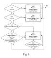
- Figure 6 illustrates an example method 600 according to some embodiments of the invention.
- the method steps of method 600 may, for example be performed by the modulation control unit 280 and the phase counter 290 of Figure 2 .
- step 610 it is determined whether the time adjustment value (TAV) is zero (i.e. no time adjustment is required).
- step 610 If the time adjustment value is zero (YES-path out of step 610), the phase is updated by adding a default value (modulus a maximal phase value) in step 620 and the process returns to step 610 to update the phase in the next filter clock cycle.
- step 610 If the time adjustment value is not zero (NO-path out of step 610), then the process proceeds to step 630 where it is determined whether the time adjustment value is positive.
- step 630 If the time adjustment value is positive (YES-path out of step 630), the phase is updated by adding the default value and the time adjustment value (modulus the maximal phase value) in step 640 and the process returns to step 610 to update the phase in the next filter clock cycle.
- step 650 it is determined whether adding the default value and the time adjustment value (no modulus) would result in a negative phase. This corresponds to the case where the FIFO 312a-j of the pulse-shaping filter 300 in Figure 3A would have to be shifted backwards, which is an unrealistic course of action. Thus, if this is the case, then the time adjustment must be postponed.
- step 650 If adding the default value and the time adjustment value (no modulus) would not result in a negative phase (NO-path out of step 650), then the process proceeds to step 660.
- step 660 it is determined whether adding twice the default value and the time adjustment value (no modulus) would result in a phase that is less than a threshold and adding twice the default value (no modulus) would result in a phase that is not less than the threshold.
- the threshold may be equal to the maximal phase value. This scenario corresponds to the case where the phase is already close to its maximum value and there is a risk of getting into the situation when the FIFO 312a-j of the pulse-shaping filter 300 in Figure 3A would have to be shifted backwards. Thus, if this is the case, then the time adjustment must be postponed.
- step 660 If this is not the case (NO-path out of step 660), then the process proceeds to step 640, where the phase is updated by adding the default value and the time adjustment value (modulus the maximal phase value), Then, the process returns to step 610 to update the phase in the next filter clock cycle.
- step 670 If, however, it was determined that there is a risk of getting into the situation when the FIFO 312a-j of the pulse shaping filter 300 in Figure 3A would have to be shifted backwards (YES-paths out of steps 650 and 660), then the time adjustment must be postponed and the process proceeds to step 670.
- step 670 the phase is updated by adding the default value (modulus the maximal phase value). Then, for the next filter clock cycle, it is determined in step 680 whether there is no longer any risk of getting into the situation when the FIFO 312a-j of the pulse shaping filter 300 in Figure 3A would have to be shifted backwards. This is determined by checking whether adding the default value and the time adjustment value (no modulus) would result in a non-negative phase that is less that the threshold.
- steps 670 and 680 are repeated for each filter clock cycle until the risk has vanished.
- step 640 the phase is updated by adding the default value and the time adjustment value (modulus the maximal phase value). Then, the process returns to step 610 to update the phase in the next filter clock cycle.
- decision step 660 is omitted.
- the NO-path out of step 650 leads directly to step 640, where the phase is updated by adding the default value and the time adjustment value (modulus the maximal phase value), Then, the process returns to step 610 to update the phase in the next filter clock cycle.
- the time adjustments value is subtracted from the phase as explained above.
- the special cases where there is a risk of getting a resulting negative phase may be handled separately as described above.
- the phase may be held at a fixed value (thus not updating with the default value) for a specified amount of time if the time adjustment value is negative.
- the specified amount of time may be a number of clock cycles equal to the floor value of the time adjustment value divided by the default value.
- the phase may be incremented by the time adjustment value modulus the default value and by the default value. Then the process may go back to incrementing the phase by the default value (compare with step 620).
- the phase may be updated using increment values that are less than the default value if the time adjustment value is negative. In these embodiments, the time adjustment is thus spread out over time. If, for example, the time adjustment value is -50 and the default value is 24, then the phase may be incremented by 14 instead of 24 in each of the subsequent 5 clock cycles. Then the process may go back to incrementing the phase by the default value (compare with step 620).
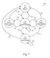
- Figure 7 is a state diagram 700 illustrating example state transitions according to some embodiments of the invention.
- the state diagram may, for example, describe operation of the modulation control unit 280 and the phase counter 290 of Figure 2 .
- the transitions in the state diagram 700 may also be compared with the method steps of method 600.
- idle state 710 there is no data to modulate.
- the state changes to state 720 via transition 711 and modulation starts.
- the state machine remains in state 720 as long as there is data to modulate and no time adjustment is needed.
- the phase is updated (repeatedly) by adding the default value (modulus a maximum phase value) as illustrated by transition 725. If there is no more data to modulate the state machine returns to the idle state 710 via transition 721.
- state 730 the state changes to state 730 via transition 722.
- the phase is updated by adding the default value and the time adjustment value (modulus the maximum phase value).
- the state changes back to state 720 via transition 731 1 unless there is no more data to modulate, in which case the state machine returns to the idle state 710 via transition 732.
- state 740 If a time adjustment is needed and the time adjustment value is negative, the state changes to state 740 via transition 723 if there is no risk of the ambiguity as described in relation to method steps 650 and 660 of method 600 in Figure 6 .
- the phase is updated by adding the default value and the time adjustment value (modulus the maximum phase value).
- the state changes back to state 720 via transition 741 unless there is no more data to modulate, in which case the state machine returns to the idle state 710 via transition 742.
- the state changes to waiting state 750 via transition 724.
- state 750 the phase is updated by adding the default value (modulus the maximum phase value), as illustrated by transition 752, until the risk has vanished or there is no more data to modulate. If there is no more data to modulate, the state machine returns to the idle state 710 via transition 753. When the risk has vanished, the state changes to state 740 via transition 751.
- state 740 the phase is updated by adding the default value and the time adjustment value (modulus the maximum phase value).
- the state changes back to state 720 via transition 741 unless there is no more data to modulate in which case the state machine returns to the idle state 710 via transition 742.
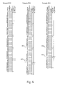
- Figure 8 illustrates three scenarios 810, 820, 830 of example time alignment adjustments according to some embodiments of the invention.
- Scenario 810 illustrates the situation when no time adjustment is needed.
- the illustrated scenario starts with Packet 0, Chip 0.
- the phase is initiated to a random phase, in this case 8.
- the default phase update value is set to 24 in this example.
- Scenario 820 illustrates the situation when a time adjustment of -82 (corresponding to one quarter of a chip) is needed.
- the time adjustment is done in the last chip in the packet (Chip 3, Packet 0).
- the effect of applying the time adjustment is that Chip 3 stays longer in the pulse shaping filter, see 822, and the next packet (Packet 1) is read later compared to scenario 810.
- the samples that are output from the pulse-shaping filter after the time adjustment are not copies of any samples before or after.
- Scenario 830 illustrates the situation when a time adjustment of 82 is needed.
- the time adjustment is also done in the last chip in the packet (Chip 3, Packet 0).
- the phase is incremented by 82 as soon as we are in Chip 3 and the time adjustment value is available (in the illustrated scenario, this occurs in the beginning of Chip 3, see 831).
- the effect of applying the time adjustment is that Chip 3 stays a shorter period in the pulse shaping filter, see 832, and the next packet (Packet 1) is read earlier compared to scenario 810.
- the time adjustment was applied in the last chip of a packet. It is to be noted that this is merely an example implementation, and that the time adjustment may be applied in any chip of a packet.
- Embodiments of the invention may be performed by general-purpose circuits associated with or integral to a receiver, such as digital signal processors (DSP), central processing units (CPU), co-processor units, or by specialized circuits such as for example application-specific integrated circuits (ASIC). All such forms are contemplated to be within the scope of the invention.
- DSP digital signal processors
- CPU central processing units
- ASIC application-specific integrated circuits
- the invention may be embodied within an electronic apparatus comprising a transmitter chain having arrangements or performing methods according to any of the embodiments of the invention.
- the electronic apparatus may, for example, be a portable or handheld mobile radio communication equipment, a mobile radio terminal, a mobile telephone, a pager, a communicator, an electronic organizer, a smartphone, a computer, an embedded drive, a mobile gaming device, or a (wrist) watch.
- a computer program product comprises a computer readable medium such as, for example, a diskette or a CD-ROM.
- the computer readable medium may have stored thereon a computer program comprising program instructions.
- the computer program may be loadable into a data-processing unit, which may, for example, be comprised in the mobile terminal 110.
- the computer program When loaded into the data-processing unit, the computer program may be stored in a memory associated with or integral to the data-processing unit.
- the computer program may, when loaded into and run by the data-processing unit, cause the data-processing unit to execute method steps according to, for example, the methods shown in Figures 5 and 6 .
Description
- The present invention relates generally to the field of adjusting time alignment of a sampled data stream. More particularly, it relates to such adjustment in a transmitter chain of an electronic communication device.
- Traditionally, the radio parts of the transmitter chain of an electronic communication device have been working in the analogue domain. Digital radio functionality may, however, also be implemented, and digital radio parts of the transmitter chain are becoming increasingly popular.
- In the course of development of digital radio chips, a digital interface standard, "DigRF, Dual-mode 2.5G / 3G, Baseband / RF IC", Interface Standard, v3.09, 22 November 2006 (henceforth denoted DigRF), has been developed to handle the interface between baseband modules and digital radio modules.
- It may be desirable to adjust the time alignment of data packets transferred from a baseband module. Not being able to adjust the time alignment can be problematic in some situations. For example, a data packet misalignment may create problems in the base station. Such problems may be highly severe, such as for example a lost connection.
- For example, if the mobile device is moving towards/away from the base station during a connection, the transmission time between the mobile device and the base station will change over time since the distance between the mobile device and the base station changes. Thus, there will be a time drift or misalignment between the data packets at the base station. Since the base station and the mobile device communications may be controlled by specific timing, drifting out of this timing may be detrimental to the connection. In connection to this example situation, reference may be made to the 3GPP (3rd Generation Partnership Project) standard documents TS 25.214 (2007-12), Section 4.3.4, TS 25.133 (2007-12), Section 7.1, and TS 25.211 (2007-12), Section 7.6.3.
-
WO 2006/115928 discloses a DigiRF interface with scheduling. - Thus, there is a need for adjusting the time alignment to compensate for misalignment.
- It should be emphasized that the term "comprises/comprising" when used in this specification is taken to specify the presence of stated features, integers, steps, or components, but does not preclude the presence or addition of one or more other features, integers, steps, components, or groups thereof.
- It is an object of the invention to obviate at least some of the above disadvantages and to provide methods and arrangements for adjusting time alignment of a sampled data stream.
- According to a first aspect of the invention, this is achieved by a method of adjusting time alignment of a sampled data stream having a first sample resolution. The method comprises transferring the sampled data stream from a baseband subsystem to a digital interface, transferring the sampled data stream from the digital interface to a digital radio comprising a pulse shaping filter modulator, modulating the sampled data stream by using the pulse shaping filter modulator, and transmitting the modulated sampled data stream. The method also comprises transferring a time adjustment control signal from the baseband subsystem to the digital radio, and the modulating step comprises a step of adjusting, based on the time adjustment control signal, the time alignment of the sampled data stream using a second sample resolution.
- In some embodiments, the second sample resolution is higher than the first sample resolution.
- In some embodiments, the method may further comprise converting, in the digital interface, the sampled data stream to an in-phase sampled data stream and a quadrature sampled data stream, and modulating the in-phase and quadrature sampled data streams separately.
- In some embodiments, the digital interface may be compliant with the DigRF standard.
- In some embodiments, the digital radio may comprise a Wideband Code Division Multiple Access - WCDMA - modulator and the WCDMA modulator may comprise the pulse shaping filter modulator.
- In some embodiments, the pulse-shaping filter may be a root raised cosine filter.
- In some embodiments, the step of adjusting the time alignment of the sampled data stream may comprise adjusting a phase of the pulse-shaping filter based on time adjustment control signal, and modifying coefficients of the pulse-shaping filter based on the adjusted phase.
- In some embodiments, the step of transferring the time adjustment control signal from the baseband subsystem to the digital radio may comprise transferring the time adjustment control signal from the baseband subsystem to the digital interface, converting the time adjustment control signal to a time adjustment value, and transferring the time adjustment value from the digital interface to the digital radio.
- In some embodiments, the method may further comprise converting the time adjustment control signal to an apply time adjustment flag, transferring the apply time adjustment flag from the digital interface to the digital radio, and performing the step of adjusting the time alignment of the sampled data stream when the apply time adjustment flag is set.
- In some embodiments, the step of adjusting the phase of the pulse shaping filter based on time adjustment control signal may comprise updating the phase of the pulse shaping filter by adding a default phase update offset value and the time adjustment value to the phase.
- In some embodiments, the method may further comprise determining whether adjusting the phase of the pulse shaping filter results in reprocessing of a sample of the sampled data stream, and, if adjusting the phase of the pulse-shaping filter results in reprocessing of a sample of the sampled data stream, postponing the step of adjusting the time alignment of the sampled data stream and updating the phase of the pulse shaping filter by adding the default phase update offset value to the phase.
- In some embodiments, the method may further comprise determining whether adding the default phase update offset value and the time adjustment value to the phase gives a first result value that is less than a threshold, and. if the first result value is less than the threshold, postponing the step of adjusting the time alignment of the sampled data stream, and updating the phase of the pulse shaping filter by adding the default phase update offset value to the phase. The threshold may be zero.
- A second aspect of the invention is a computer program product comprising a computer readable medium, having thereon a computer program comprising program instructions, the computer program being loadable into a data-processing unit and adapted to cause the data-processing unit to execute at least the step of adjusting the time alignment according to the first aspect of the invention when the computer program is run by the data-processing unit.
- A third aspect of the invention is an arrangement for adjusting time alignment of a sampled data stream having a first sample resolution. The arrangement comprises a baseband subsystem, a digital interface, and a digital radio comprising a modulator and a transmitter. The baseband subsystem is adapted to transfer the sampled data stream to the digital interface, the digital interface is adapted to transfer the sampled data stream to the digital radio, the modulator is adapted to modulate the sampled data stream, and the transmitter is adapted to transmit the modulated sampled data stream. The baseband subsystem is adapted to transfer a time adjustment control signal to the digital radio, and the modulator is adapted to adjust, based on the time adjustment control signal, the time alignment of the sampled data stream using a second sample resolution.
- In some embodiments, the modulator comprises a Wideband Code Division Multiple Access - WCDMA - modulator and the WCDMA modulator comprises a pulse shaping filter modulator.
- In some embodiments, the modulator may comprise a phase counter adapted to provide a phase of the pulse shaping filter, and a modulation control unit adapted to adjust the phase based on time adjustment control signal. In some embodiments, the pulse shaping filter modulator may be adapted to modify coefficients of the pulse-shaping filter based on the adjusted phase.
- In some embodiments, the third aspect of the invention may additionally have features identical with or corresponding to any of the various features as explained above for the first aspect of the invention.
- A fourth aspect of the invention is an electronic device comprising the arrangement of the third aspect of the invention. In some embodiments, the electronic device may be a mobile terminal.
- The first sample resolution may be defined as the smallest possible time alignment adjustment that can be made in the baseband subsystem. The second sample resolution may be defined as the smallest possible time alignment adjustment that can be made in the digital radio according to embodiments of the invention. Thus, that the second sample resolution is higher than the first sample resolution in some embodiments means that a time alignment adjustment can be made in smaller steps if using the second sample resolution rather than the first sample resolution.
- One of the advantages of embodiments of the invention is that time alignment of a sampled data stream may be achieved.
- A further advantage of embodiments of the invention is that the alignment can be achieved with high resolution.
- A further advantage of embodiments of the invention is that timing adjustments are achievable that are smaller than the distance between the samples that are transferred between the baseband module and the radio module. This allows for fine-tuning of the timing adjustments.
- A further advantage of embodiments of the invention is that mechanisms are provided to prevent ambiguities at packet boundaries and at chip boundaries.
- A further advantage of embodiments of the invention is that the transmitted signal does not contain sharp changes. Instead, the adjustment may be made so that the effect of the adjustment is smoothed in the transmitted signal.
- A further advantage of embodiments of the invention is that a straightforward implementation is offered.
- A further advantage of embodiments of the invention is that a low complexity implementation is offered.
- Further objects, features and advantages of the invention will appear from the following detailed description of embodiments of the invention, with reference being made to the accompanying drawings, in which:
-
Fig. 1 is a schematic front view of a mobile terminal connected, through a radio link, to a base station site, wherein the mobile terminal may comprise arrangements according to some embodiments of the invention; -
Fig. 2 is a block diagram illustrating parts of an example arrangement according to some embodiments of the invention; -
Fig. 3A is a block diagram illustrating an example pulse-shaping filter according to some embodiments of the invention; -
Fig. 3B is a schematic diagram illustrating time alignment adjustments according to embodiments of the invention; -
Fig. 4 is a plot illustrating an example pulse shaping filter function according to some embodiments of the invention; -
Fig. 5 is a flow chart illustrating example method steps according to some embodiments of the invention; -
Fig. 6 is a flow chart illustrating example method steps according to some embodiments of the invention; -
Fig. 7 is a state diagram illustrating example state transitions according to some embodiments of the invention; and -
Fig. 8 is a schematic figure illustrating example time alignment adjustments according to some embodiments of the invention. - In the following, example embodiments of the invention will be described in which a time misalignment of a data stream is adjusted. The data stream may be a transmit data stream in a Wideband Code Division Multiple Access (WCDMA) transmitter. However, the invention is not limited to such cases. Contrarily, embodiments of the invention may be used in transmitter chains that use other transmission techniques, such as, for example, Orthogonal Frequency Division Multiplexing (OFDM).
- As mentioned before, there may be a need, in some circumstances, for adjusting the time alignment to compensate for misalignment of the data stream. In some example scenarios, misalignment and/or congestion in the baseband module may be a reason that time alignment adjustment is needed. In some scenarios, the movement of a mobile communication device may be a reason that time alignment adjustment is needed as explained above. If, for example, the baseband stream misalignment is one chip, the call will be dropped according to some scenarios. In the 3GPP standard, adjustments of less than one-quarter chip are allowed (see TS 25.133 (2007-12), Section 7.1).
- One way of achieving a time adjustment is to perform an adjustment in the baseband module/sub-system or in the digital interface. In general, however, this has the disadvantage that adjustments can only be made with a resolution of one chip.
- Thus, this is not a preferable solution since omitting a full chip in uplink may be problematic. It may, for example, cause sharp changes in the transmitted signal. Base stations may not be programmed to track large sudden changes in the uplink timing. A large change may result in losing the connection with the mobile phone.
- Introduction of a digital radio in the transmitter chain opens up the possibility of moving the modulator from the baseband sub-system to the digital radio. A modulator of a digital radio may have a resolution that is substantially higher than one chip.
- Thus, if, for example, the modulation is being done using a pulse shaping filter which has the functionality of a 325 times over-sampled root raised cosine filter, then the time adjustment may be performed with a resolution of 1/325 of a chip.
- Embodiments of the invention suggest that time adjustment is made in association with the digital radio modulator. In these embodiments the resolution of the time adjustment increases. In some embodiments, the resolution increases from one chip to 1/325 chip and adjustments of up to one quarter of a chip may be achieved. It should be noted that a resolution of 1/325 and a maximum adjustment of one quarter of a chip are merely example values. Other example values may be handled by some embodiments of the invention. Maximum adjustment values may be imposed by a communication standard applied by an example embodiment. For example, one quarter of a chip adjustment is imposed by the 3GPP standard document TS 25.133 (2007-12), Section 7.1.
- In some embodiments, time adjustment is achieved by modifying coefficients of a pulse-shaping filter used in the digital radio modulator in a controlled manner. The pulse-shaping filter may practice over-sampling of the data stream, hence providing a higher resolution for the time adjustment. In some embodiments, this pulse-shaping filter is a poly-phase filter used for up-sampling in the modulator. In some embodiments, the pulse shaping filter gives the functionality of a 325 times over-sampled root raised cosine filter multiplied with a Kaiser window with parameter 2.0.
- When a time adjustment is needed, the baseband module may send the required adjustment value to the digital interface, which in turn may forward the adjustment value to the pulse shaping filter control. A strobe indicating when to apply the adjustment may also be provided.
- In some embodiments, the modulator accepts timing adjustment values up to and including ±1/4 chips, with a timing adjustment step size of 1/325 chip.
-
Figure 1 illustrates an examplemobile terminal 110 connected, through aradio link 120, to abase station site 130. Thebase station site 130 comprises one ormore antennas 135 and at least onebase station 150. Themobile terminal 110 may comprise an arrangement according to embodiments of the invention. - The
mobile terminal 110 is illustrated as a mobile telephone in a schematic front view. This examplemobile terminal 110 comprises anantenna 111 mounted on the housing of the apparatus. Alternatively, themobile terminal 110 may have an internal antenna mounted within the housing of the apparatus. Themobile terminal 110 may even comprise multiple antennas. Themobile terminal 110 may further comprise a display, a keypad, a loudspeaker, and a microphone, which together provides a man-machine interface for operating themobile terminal 110. - The example
mobile terminal 110 is adapted to connect to a mobile telecommunication network via thewireless link 120 to theradio base station 150. Hence, a user of themobile terminal 110 may use conventional circuit-switched telecommunication services such as voice calls, data calls, video calls, and fax transmissions, and/or packet-based services such as electronic messaging, VoIP, Internet browsing, electronic commerce, etc. To this end, themobile terminal 110 and thebase station 150 may be compliant with at least one mobile telecommunication standard, for instance UMTS or UMTS LTE. -
Figure 2 illustrates parts of anexample arrangement 200 according to some embodiments of the invention. The illustratedarrangement 200 may be comprised in an electronic communication device, such as themobile terminal 110 illustrated inFigure 1 . - The
arrangement 200 comprises abaseband module 210, which is adapted to produce a digital data stream. At 212 the digital data stream may be transferred to adigital interface 220, such as a DigRF interface. Thedigital interface 220 may be adapted to split the digital data stream into an in-phase and a quadrature data stream. At 222 these in-phase and quadrature data streams are transferred to adigital radio 230. - The digital interface specifies the form and timing of communication between baseband and radio modules. In Dig RF, data may be sent in packets. Each packet may contain eight samples at chip rate, meaning that one sample corresponds to one chip. The chip rate may be 3.84 Msamples per second. Samples may be represented by 12 or 16 bits. The samples may be divided equally between in-phase and quadrature branches. Thus, each packet may contain 4 samples (chips). The TX (transmit) data interface in Dig RF carries both data to be transmitted and RF IC (radio frequency integrated circuit) control information. More information regarding standard packing in the uplink may be found in "DigRF, Dual-mode 2.5G / 3G, Baseband / RF IC", Interface Standard, v3.09, 22 November 2006, section 7.1.3.
- The
digital radio 230 comprises amodulator 240, such as a wideband modulator in the case of WCDMA, and transmitter circuitry (TX) 250. Themodulator 240 is adapted to up-sample and modulate the in-phase and quadrature data streams respectively and thetransmitter circuitry 250 is adapted to transmit the modulated data steams via one ormore antennas 260. - Before the in-phase and quadrature data streams enter the
modulator 240, they may undergo rounding and saturation operations. The in-phase and quadrature data streams then enter themodulator 240, which comprises a pulse shaping filter modulator (PSFM) 270. The pulse shapingfilter modulator 270 is adapted to process the in-phase and quadrature data streams separately using two pulse shaping filters (PSF) 271 a and 271 b. Themodulator 240 also comprises a modulation control unit (MCU) 280 and a phase counter (Ph Cntr) 290. Themodulation control unit 280 and thephase counter 290 are operatively connected at 284. Themodulation control unit 280 and thephase counter 290 are operatively connected to the pulse shapingfilter modulator 270 at 282 and 292 respectively. - It should be noted that, in other embodiments, the digital interface might not split the digital data stream into an in-phase and a quadrature data stream. Instead the digital data stream is transferred to the
digital radio 230 via a single connection and thedigital radio 230 processes the digital data stream as a single data stream. - A time adjustment control signal may be transferred from the
baseband module 210 to thedigital interface 220 as shown at 214. The time adjustment control signal may, for example, be included in the RF IC control information in DigRF. This time adjustment control signal may indicate whether time adjustment is needed. In some embodiments, it may also indicate when the time adjustment should be applied. In some embodiments, the time adjustment control signal is associated with a packet of the data stream. The timing of the packet sent from the baseband module to the digital radio may, for example, be adjusted at the same time as the control command is sent to the digital radio. - The
digital interface 220 may convert the time adjustment control signal to a time adjustment value and transfer this value to the digital radio as shown at 223. Thedigital interface 220 may also convert the time adjustment control signal to an apply time adjustment flag and transfer this flag to the digital radio as shown at 224. In some embodiments, there is no indication of when to apply the adjustment in the time adjustment control signal. In such embodiments, the apply time adjustment flag may be created by thedigital interface 220. In yet some embodiments, thedigital interface 220 does not convert the time adjustment signal. Instead the time adjustment signal is simply forwarded to thedigital radio 230. -
Figure 3A illustrates an example implementation of a pulse-shapingfilter 300 according to some embodiments of the invention. The pulse-shapingfilter 300 may for example be comprised in the pulse shaping filters 271 a and 271 b ofFigure 2 . - The signal at the
input 310 of the pulse-shapingfilter 300 may be the in-phase or quadrature data stream received from thedigital interface 220 ofFigure 2 . In a conventional manner, each symbol (chip) of the input signal is shifted along a first-in first-out (FIFO) shift register, which is made up bymemory elements 312a-j. The symbols are shifted one step each time thecontrol signal 394 is set. - The content of each
memory element 312a-j is multiplied by acorresponding filter coefficient 314a-j. The results of the multiplications are accumulated inadder 317 and output from the pulse-shapingfilter 300 at 319, possibly after rounding in 318. - As can be seen in
Figure 3A , eachcoefficient 314a-j is variable. Each coefficient may, for example comprise a table of coefficient values. A phase, illustrated at 392, determines the coefficient value that should be used. For example, the phase may specify which value in a table to apply in the multiplication. The phase is updated during each filter clock cycle. A new result is output at 319 for each update of the phase. - The illustrated pulse-shaping
filter 300 has a poly-phase structure, which reduces implementation cost. The illustrated poly-phase structure has a filter bank of 325 coefficient vectors. Each vector consists of 10 coefficients values. The 325 coefficient vectors differ in sample phase, representing a time shift of (0...324)/325 chip, i.e. each change of vector bank changes the phase by 1/325 chip. - The phase is determined by a
phase calculation unit 340 and is output to the coefficient tables at 392. The phase calculation unit may comprise themodulation control unit 280 and thephase counter 290 ofFigure 2 . Thephase control unit 340 receives information regarding the time adjustment value and the apply time adjustment flag as illustrated at 323 and 324 (compare with 223 and 224 ofFigure 2 ). - It should be noted that that the time alignment adjustment according to embodiments of the invention may be achieved also when other types of filters are used. Thus, the invention is not limited to pulse shaping filters of a poly-phase structure.
-
Figure 3B illustrates an example with 8 times chip rate over-sampling. In this example, an adjustment of an eighth of a chip will be equivalent to repeating one sample or ignoring one sample depending on if the required adjustment is negative or positive. InFigure 3B , two chips (each comprising 8 samples) are shown in different adjustment situations, wherein 351 represents an adjustment of-1/4 chip, 352 represents an adjustment of -1/8 chip, 353 represents a situation with no adjustment, 354 represents an adjustment of 1/8 chip, and 355 represents an adjustment of 1/4 chip. -
Figure 4 illustrates an example pulse shaping filter function 400 according to some embodiments of the invention. This example filter function 400 is a root raised cosine function and may be used in the pulse-shapingfilter 300 ofFigure 3A . The filter function 400 is illustrated with ten coefficient tables (compare 314a j ofFigure 3A ), and each coefficient table comprises 325 coefficient values in this example. - The operation of an arrangement according to embodiments of the invention will now be described with reference to
Figures 2 ,3 and4 . -
Phase calculation pulse shaping filters pulse shaping filter - The example pulse-shaping
filter 300 is clocked with a 52MHz clock. The input to the filter is samples at chip rate, e.g. 3.84 MHz, each represented with, for example, 12 bits. The index to the filter vector bank may be updated by the default value 24 each 1/52MHz cycle, this is because 52/3.84 = 325/24. Thus, with these example numerical values, the following pseudo code may illustrate an example phase calculation algorithm:
        phase <= 0;
         while (1) loop
            t_phase := phase+24;
            if t_phase >= 325 then phase <= t_phase-325;
         shift_en <= '1';
            else phase <= t_phase; shift_en <= '0';
         end loop;
Claims (28)
- A method of adjusting time alignment of a sampled data stream having a first sample resolution comprising:transferring (510) the sampled data stream from a baseband subsystem to a digital interface;transferring (520) the sampled data stream from the digital interface to a digital radio comprising a pulse shaping filter modulator;modulating (530) the sampled data stream by using the pulse shaping filter modulator; andtransmitting (540) the modulated sampled data stream;characterized bytransferring (515, 525) a time adjustment control signal from the baseband sub-system to the digital radio; andthe modulating step comprising a step of adjusting, based on the time adjustment control signal, the time alignment of the sampled data stream using a second sample resolution.
- The method of claim 1, wherein the second sample resolution is higher than the first sample resolution.
- The method of any of claims 1 through 2, further comprising:converting, in the digital interface, the sampled data stream to an in-phase sampled data stream and a quadrature sampled data stream; andmodulating the in-phase and quadrature sampled data streams separately.
- The method of any of claims 1 through 3, wherein the digital interface is compliant with the DigRF standard, v3.09.
- The method of any of claims 1 through 4, wherein the digital radio comprises a Wideband Code Division Multiple Access, WCDMA, modulator and the WCDMA modulator comprises the pulse shaping filter modulator.
- The method of any of claims 1 through 5, wherein a pulse-shaping filter of the pulse-shaping filter modulator is a root raised cosine filter.
- The method of any of claims 1 through 5, wherein the step of adjusting the time alignment of the sampled data stream comprises:adjusting a phase of a pulse-shaping filter of the pulse shaping filter modulator based on time adjustment control signal; andmodifying coefficients of the pulse shaping filter based on the adjusted phase.
- The method of claim 7, wherein the step of transferring the time adjustment control signal from the baseband subsystem to the digital radio comprises:transferring (515) the time adjustment control signal from the baseband subsystem to the digital interface;converting the time adjustment control signal to a time adjustment value; andtransferring (525) the time adjustment value from the digital interface to the digital radio.
- The method of claim 8, further comprising:converting the time adjustment control signal to an apply time adjustment flag;transferring (525) the apply time adjustment flag from the digital interface to the digital radio; andperforming the step of adjusting the time alignment of the sampled data stream when the apply time adjustment flag is set.
- The method of any of claims 8 through 9, wherein the step of adjusting the phase of the pulse shaping filter based on time adjustment control signal comprises:updating (640) the phase of the pulse shaping filter by adding a default phase update offset value and the time adjustment value to the phase.
- The method of claim 10, further comprising:determining (650, 660) whether adjusting the phase of the pulse shaping filter results in reprocessing of a sample of the sampled data stream; andif adjusting the phase of the pulse-shaping filter results in reprocessing of a sample of the sampled data stream:postponing the step of adjusting the time alignment of the sampled data stream; andupdating (670) the phase of the pulse-shaping filter by adding the default phase update offset value to the phase.
- The method of claim 10, further comprising:determining (650) whether adding the default phase update offset value and the time adjustment value to the phase gives a first result value that is less than a threshold; andif the first result value is less than the threshold:postponing the step of adjusting the time alignment of the sampled data stream; andupdating (670) the phase of the pulse-shaping filter by adding the default phase update offset value to the phase.
- The method of claim 12, wherein the threshold is zero.
- A computer program product comprising a computer readable medium, having thereon a computer program comprising program instructions, the computer program being loadable into a data-processing unit and adapted to cause the data-processing unit to execute at least the method of adjusting the time alignment according to any of claims 1 to 13 when the computer program is run by the data-processing unit.
- An arrangement for adjusting time alignment of a sampled data stream having a first sample resolution comprising:a baseband subsystem (210);a digital interface (220); anda digital radio (230) comprising a modulator (240) and a transmitter (250);wherein the baseband subsystem (210) is adapted to transfer the sampled data stream to the digital interface, the digital interface (220) is adapted to transfer the sampled data stream to the digital radio, the modulator (240) is adapted to modulate the sampled data stream, and the transmitter (250) is adapted to transmit the modulated sampled data stream;characterized in thatthe baseband subsystem (210) is adapted to transfer a time adjustment control signal to the digital radio; andthe modulator (240) is adapted to adjust, based on the time adjustment control signal, the time alignment of the sampled data stream using a second sample resolution.
- The arrangement of claim 15, wherein the second sample resolution is higher than the first sample resolution.
- The arrangement of any of claims 15 through 16, wherein the digital interface (220) is further adapted to convert the sampled data stream to an in-phase sampled data stream and a quadrature sampled data stream, and the modulator (240) is further adapted to modulate the in-phase and quadrature sampled data streams separately.
- The arrangement of any of claims 15 through 17, wherein the digital interface (220) is compliant with the DigRF standard, v3.09.
- The arrangement of any of claims 15 through 18, wherein the modulator (240) comprises a Wideband Code Division Multiple Access, WCDMA, modulator and the WCDMA modulator comprises a pulse shaping filter modulator (270).
- The arrangement of claim 19, wherein a pulse-shaping filter of the pulse-shaping filter modulator is a root raised cosine filter (400).
- The arrangement of claim 19, wherein the modulator (240) comprises:a phase counter (290) adapted to provide a phase of a pulse-shaping filter of the pulse shaping filter modulator; anda modulation control unit (280) adapted to adjust the phase based on time adjustment control signal;and wherein the pulse shaping filter modulator (270) is adapted to modify coefficients of the pulse-shaping filter based on the adjusted phase.
- The arrangement of claim 21, wherein the baseband subsystem (210) is further adapted to transfer the time adjustment control signal to the digital interface, and the digital interface (220) is further adapted to convert the time adjustment control signal to a time adjustment value and to transfer the time adjustment value to the digital radio.
- The arrangement of claim 22, wherein the digital interface (220) is further adapted to convert the time adjustment control signal to an apply time adjustment flag and to transfer the apply time adjustment flag to the digital radio, and wherein the modulator (240) is adapted to adjust the time alignment of the sampled data stream when the apply time adjustment flag is set.
- The arrangement of any of claims 22 through 23, wherein the modulation control unit (280) is further adapted to update the phase of the pulse shaping filter by adding a default phase update offset value and the time adjustment value to the phase.
- The arrangement of claim 24, wherein the modulation control unit (280) is further adapted to:determine whether adjusting the phase of the pulse shaping filter results in reprocessing of a sample of the sampled data stream; andif adjusting the phase of the pulse-shaping filter results in reprocessing of a sample of the sampled data stream:postpone adjustment of the time alignment of the sampled data stream; andinstruct the phase counter (290) to update the phase of the pulse-shaping filter by adding the default phase update offset value to the phase.
- The arrangement of claim 24, wherein the modulation control unit (280) is further adapted to:determine whether adding the default phase update offset value and the time adjustment value to the phase gives a first result value that is less than a threshold; andif the first result value is less than the threshold:postpone adjustment of the time alignment of the sampled data stream; andinstruct the phase counter (290) to update the phase of the pulse-shaping filter by adding the default phase update offset value to the phase.
- An electronic device comprising the arrangement of any of claims 15 through 26.
- The electronic device of claim 27, wherein the electronic device is a mobile terminal (110).
Priority Applications (4)
| Application Number | Priority Date | Filing Date | Title |
|---|---|---|---|
| EP08153563A EP2106058B1 (en) | 2008-03-28 | 2008-03-28 | Method and arrangement for adjusting time alignment of a sampled data stream |
| PCT/EP2009/053649 WO2009118405A1 (en) | 2008-03-28 | 2009-03-27 | Method and arrangement for adjusting time alignment of a sampled data stream |
| ARP090101105A AR071098A1 (en) | 2008-03-28 | 2009-03-27 | METHOD AND PROVISION TO ADJUST THE TIME ALIGNMENT OF A SAMPLED DATA FLOW |
| US12/934,728 US8509206B2 (en) | 2008-03-28 | 2009-03-27 | Method and arrangement for adjusting time alignment of a sampled data stream |
Applications Claiming Priority (1)
| Application Number | Priority Date | Filing Date | Title |
|---|---|---|---|
| EP08153563A EP2106058B1 (en) | 2008-03-28 | 2008-03-28 | Method and arrangement for adjusting time alignment of a sampled data stream |
Publications (2)
| Publication Number | Publication Date |
|---|---|
| EP2106058A1 EP2106058A1 (en) | 2009-09-30 |
| EP2106058B1 true EP2106058B1 (en) | 2012-06-27 |
Family
ID=39712570
Family Applications (1)
| Application Number | Title | Priority Date | Filing Date |
|---|---|---|---|
| EP08153563A Not-in-force EP2106058B1 (en) | 2008-03-28 | 2008-03-28 | Method and arrangement for adjusting time alignment of a sampled data stream |
Country Status (4)
| Country | Link |
|---|---|
| US (1) | US8509206B2 (en) |
| EP (1) | EP2106058B1 (en) |
| AR (1) | AR071098A1 (en) |
| WO (1) | WO2009118405A1 (en) |
Families Citing this family (17)
| Publication number | Priority date | Publication date | Assignee | Title |
|---|---|---|---|---|
| US7843859B1 (en) * | 2008-09-23 | 2010-11-30 | Netlogic Microsystems, Inc. | Analog echo canceller with filter banks |
| US20110075648A1 (en) * | 2009-09-30 | 2011-03-31 | Hongwei Kong | Method and system for wcdma/hsdoa timing adjustment |
| ES2796833T3 (en) * | 2011-06-10 | 2020-11-30 | Airbus Defence & Space Ltd | Non-synchronous data stream alignment |
| US9341676B2 (en) | 2011-10-07 | 2016-05-17 | Alcatel Lucent | Packet-based propagation of testing information |
| US8737551B1 (en) | 2012-11-06 | 2014-05-27 | Motorola Mobility Llc | Synchronizing receive data over a digital radio frequency (RF) interface |
| US9231719B2 (en) | 2013-03-12 | 2016-01-05 | Hamilton Sundstrand Corporation | Method and apparatus for multiplexed time aligned analog input sampling |
| CN107000686B (en) | 2014-09-29 | 2019-01-29 | 莱尔德无线技术(上海)有限公司 | The method of remote information process device and the ignition event for detecting vehicle |
| US10158509B2 (en) | 2015-09-23 | 2018-12-18 | Innophase Inc. | Method and apparatus for polar receiver with phase-amplitude alignment |
| US9673829B1 (en) | 2015-12-02 | 2017-06-06 | Innophase, Inc. | Wideband polar receiver architecture and signal processing methods |
| US10122397B2 (en) | 2017-03-28 | 2018-11-06 | Innophase, Inc. | Polar receiver system and method for Bluetooth communications |
| US10503122B2 (en) | 2017-04-14 | 2019-12-10 | Innophase, Inc. | Time to digital converter with increased range and sensitivity |
| US10108148B1 (en) * | 2017-04-14 | 2018-10-23 | Innophase Inc. | Time to digital converter with increased range and sensitivity |
| US10840921B2 (en) | 2018-09-07 | 2020-11-17 | Innophase Inc. | Frequency control word linearization for an oscillator |
| US10622959B2 (en) | 2018-09-07 | 2020-04-14 | Innophase Inc. | Multi-stage LNA with reduced mutual coupling |
| US11095296B2 (en) | 2018-09-07 | 2021-08-17 | Innophase, Inc. | Phase modulator having fractional sample interval timing skew for frequency control input |
| WO2020146408A1 (en) | 2019-01-07 | 2020-07-16 | Innophase, Inc. | Using a multi-tone signal to tune a multi-stage low-noise amplifier |
| US10728851B1 (en) | 2019-01-07 | 2020-07-28 | Innophase Inc. | System and method for low-power wireless beacon monitor |
Family Cites Families (9)
| Publication number | Priority date | Publication date | Assignee | Title |
|---|---|---|---|---|
| US6915318B2 (en) * | 2002-04-29 | 2005-07-05 | Lsi Logic Corporation | Interpolator |
| US7054396B2 (en) * | 2002-08-20 | 2006-05-30 | Rf Micro Devices, Inc. | Method and apparatus for multipath signal compensation in spread-spectrum communications systems |
| EP1776817B1 (en) * | 2004-07-29 | 2009-03-25 | Nxp B.V. | Enhanced bit mapping for digital interface of a wireless communication equipment in multi-time slot and multi-mode operation |
| US7583937B2 (en) * | 2005-04-26 | 2009-09-01 | Silicon Laboratories Inc. | Digital interface and related event manager for integrated circuits |
| US20080195920A1 (en) * | 2007-02-13 | 2008-08-14 | Freescale Semiconductor, Inc. | Self-test structure and method of testing a digital interface |
| US8023556B2 (en) * | 2007-03-30 | 2011-09-20 | Silicon Laboratories Inc. | Autonomously generating ramp profiles in a transceiver |
| US7738491B2 (en) * | 2007-07-16 | 2010-06-15 | Infineon Technologies Ag | Frame structure, method for organizing data and method for transmitting data |
| US7941118B2 (en) * | 2007-08-01 | 2011-05-10 | Broadcom Corporation | Method and apparatus to process dedicated physical control channel (DPCCH) in a transmit antenna diversity (TXDIV) rake finger |
| GB0721427D0 (en) * | 2007-10-31 | 2007-12-12 | Icera Inc | Processing signals in a wireless newtwork |
-
2008
- 2008-03-28 EP EP08153563A patent/EP2106058B1/en not_active Not-in-force
-
2009
- 2009-03-27 WO PCT/EP2009/053649 patent/WO2009118405A1/en active Application Filing
- 2009-03-27 US US12/934,728 patent/US8509206B2/en active Active
- 2009-03-27 AR ARP090101105A patent/AR071098A1/en active IP Right Grant
Also Published As
| Publication number | Publication date |
|---|---|
| AR071098A1 (en) | 2010-05-26 |
| EP2106058A1 (en) | 2009-09-30 |
| US20110019657A1 (en) | 2011-01-27 |
| WO2009118405A1 (en) | 2009-10-01 |
| US8509206B2 (en) | 2013-08-13 |
Similar Documents
| Publication | Publication Date | Title |
|---|---|---|
| EP2106058B1 (en) | Method and arrangement for adjusting time alignment of a sampled data stream | |
| US8031586B2 (en) | Method and apparatus for transmitter timing adjustment | |
| US6411611B1 (en) | Communication systems, communication methods and a method of communicating data within a DECT communication system | |
| CN1087885C (en) | demodulator for demodulation spread spectrum signal and its method | |
| US8619840B2 (en) | Apparatus and methods for sampling rate conversion for wireless transceivers | |
| EP1894331B1 (en) | Synchronizing a modem and vocoder of a mobile station | |
| US20030072284A1 (en) | Sample rate change between single-carrier and multi-carrier waveforms | |
| CZ285903B6 (en) | Method of making duplex communication and subscriber unit making the same | |
| WO2006060501A1 (en) | Method and system for scaling a multi-channel signal | |
| US6463110B1 (en) | Timing synchronization in a communication device | |
| EP1113576A2 (en) | Digital matched filter despreading received signal and mobile wireless terminal using digital matched filter | |
| EP1628407A2 (en) | Digital baseband transmitter with digital RF/IF support in GSM/GPRS/EDGE compliant handsets | |
| EP2242227A1 (en) | Method and device for processing a digital complex modulated signal within a polar modulation transmission chain. | |
| EP0960521A1 (en) | Apparatus and method for adapting an echo canceller in a communication system | |
| WO2002060146A1 (en) | Method of implementing modulation and modulator | |
| WO2018137219A1 (en) | Information transmission method and apparatus | |
| US7885357B1 (en) | Apparatus for signal detection to enhance performance of a receiver and method therefor | |
| Sawai et al. | General-purpose symbol rate and symbol timing estimation method by using multi-resolution analysis based on wavelet transform for multimode software radio | |
| JP2001244848A (en) | Spread spectrum communication receiving device | |
| EP2461525A1 (en) | Method and appratus for aligning data frames in a transceiver device | |
| JP2004056747A (en) | Afc function and its equipment of orthogonal frequency division multiplex | |
| CN106936512A (en) | Optical signal transmitter and light signal receiving and optical fiber telecommunications system | |
| NL9700008A (en) | Subscriber equipment for digital radio communications system | |
| EP3391546A1 (en) | Constant amplitude interpolation of zadoff-chu sequences |
Legal Events
| Date | Code | Title | Description |
|---|---|---|---|
| PUAI | Public reference made under article 153(3) epc to a published international application that has entered the european phase |
Free format text: ORIGINAL CODE: 0009012 |
|
| AK | Designated contracting states |
Kind code of ref document: A1 Designated state(s): AT BE BG CH CY CZ DE DK EE ES FI FR GB GR HR HU IE IS IT LI LT LU LV MC MT NL NO PL PT RO SE SI SK TR |
|
| AX | Request for extension of the european patent |
Extension state: AL BA MK RS |
|
| 17P | Request for examination filed |
Effective date: 20100330 |
|
| AKX | Designation fees paid |
Designated state(s): AT BE BG CH CY CZ DE DK EE ES FI FR GB GR HR HU IE IS IT LI LT LU LV MC MT NL NO PL PT RO SE SI SK TR |
|
| 17Q | First examination report despatched |
Effective date: 20110920 |
|
| REG | Reference to a national code |
Ref country code: DE Ref legal event code: R079 Ref document number: 602008016678 Country of ref document: DE Free format text: PREVIOUS MAIN CLASS: H04L0007000000 Ipc: H04W0056000000 |
|
| GRAP | Despatch of communication of intention to grant a patent |
Free format text: ORIGINAL CODE: EPIDOSNIGR1 |
|
| RIC1 | Information provided on ipc code assigned before grant |
Ipc: H04B 1/40 20060101ALI20120103BHEP Ipc: H04W 56/00 20090101AFI20120103BHEP Ipc: H04L 25/03 20060101ALN20120103BHEP |
|
| RIC1 | Information provided on ipc code assigned before grant |
Ipc: H04W 56/00 20090101AFI20120110BHEP Ipc: H04L 25/03 20060101ALN20120110BHEP Ipc: H04B 1/40 20060101ALI20120110BHEP |
|
| GRAS | Grant fee paid |
Free format text: ORIGINAL CODE: EPIDOSNIGR3 |
|
| GRAA | (expected) grant |
Free format text: ORIGINAL CODE: 0009210 |
|
| AK | Designated contracting states |
Kind code of ref document: B1 Designated state(s): AT BE BG CH CY CZ DE DK EE ES FI FR GB GR HR HU IE IS IT LI LT LU LV MC MT NL NO PL PT RO SE SI SK TR |
|
| REG | Reference to a national code |
Ref country code: GB Ref legal event code: FG4D |
|
| REG | Reference to a national code |
Ref country code: CH Ref legal event code: EP |
|
| REG | Reference to a national code |
Ref country code: AT Ref legal event code: REF Ref document number: 564724 Country of ref document: AT Kind code of ref document: T Effective date: 20120715 |
|
| REG | Reference to a national code |
Ref country code: IE Ref legal event code: FG4D |
|
| REG | Reference to a national code |
Ref country code: DE Ref legal event code: R096 Ref document number: 602008016678 Country of ref document: DE Effective date: 20120830 |
|
| PG25 | Lapsed in a contracting state [announced via postgrant information from national office to epo] |
Ref country code: FI Free format text: LAPSE BECAUSE OF FAILURE TO SUBMIT A TRANSLATION OF THE DESCRIPTION OR TO PAY THE FEE WITHIN THE PRESCRIBED TIME-LIMIT Effective date: 20120627 Ref country code: LT Free format text: LAPSE BECAUSE OF FAILURE TO SUBMIT A TRANSLATION OF THE DESCRIPTION OR TO PAY THE FEE WITHIN THE PRESCRIBED TIME-LIMIT Effective date: 20120627 Ref country code: SE Free format text: LAPSE BECAUSE OF FAILURE TO SUBMIT A TRANSLATION OF THE DESCRIPTION OR TO PAY THE FEE WITHIN THE PRESCRIBED TIME-LIMIT Effective date: 20120627 |
|
| REG | Reference to a national code |
Ref country code: NL Ref legal event code: T3 |
|
| REG | Reference to a national code |
Ref country code: AT Ref legal event code: MK05 Ref document number: 564724 Country of ref document: AT Kind code of ref document: T Effective date: 20120627 |
|
| REG | Reference to a national code |
Ref country code: NO Ref legal event code: T2 Effective date: 20120627 |
|
| REG | Reference to a national code |
Ref country code: LT Ref legal event code: MG4D Effective date: 20120627 |
|
| PG25 | Lapsed in a contracting state [announced via postgrant information from national office to epo] |
Ref country code: LV Free format text: LAPSE BECAUSE OF FAILURE TO SUBMIT A TRANSLATION OF THE DESCRIPTION OR TO PAY THE FEE WITHIN THE PRESCRIBED TIME-LIMIT Effective date: 20120627 Ref country code: GR Free format text: LAPSE BECAUSE OF FAILURE TO SUBMIT A TRANSLATION OF THE DESCRIPTION OR TO PAY THE FEE WITHIN THE PRESCRIBED TIME-LIMIT Effective date: 20120928 Ref country code: HR Free format text: LAPSE BECAUSE OF FAILURE TO SUBMIT A TRANSLATION OF THE DESCRIPTION OR TO PAY THE FEE WITHIN THE PRESCRIBED TIME-LIMIT Effective date: 20120627 Ref country code: SI Free format text: LAPSE BECAUSE OF FAILURE TO SUBMIT A TRANSLATION OF THE DESCRIPTION OR TO PAY THE FEE WITHIN THE PRESCRIBED TIME-LIMIT Effective date: 20120627 |
|
| PG25 | Lapsed in a contracting state [announced via postgrant information from national office to epo] |
Ref country code: CY Free format text: LAPSE BECAUSE OF FAILURE TO SUBMIT A TRANSLATION OF THE DESCRIPTION OR TO PAY THE FEE WITHIN THE PRESCRIBED TIME-LIMIT Effective date: 20120627 Ref country code: RO Free format text: LAPSE BECAUSE OF FAILURE TO SUBMIT A TRANSLATION OF THE DESCRIPTION OR TO PAY THE FEE WITHIN THE PRESCRIBED TIME-LIMIT Effective date: 20120627 Ref country code: AT Free format text: LAPSE BECAUSE OF FAILURE TO SUBMIT A TRANSLATION OF THE DESCRIPTION OR TO PAY THE FEE WITHIN THE PRESCRIBED TIME-LIMIT Effective date: 20120627 Ref country code: EE Free format text: LAPSE BECAUSE OF FAILURE TO SUBMIT A TRANSLATION OF THE DESCRIPTION OR TO PAY THE FEE WITHIN THE PRESCRIBED TIME-LIMIT Effective date: 20120627 Ref country code: IS Free format text: LAPSE BECAUSE OF FAILURE TO SUBMIT A TRANSLATION OF THE DESCRIPTION OR TO PAY THE FEE WITHIN THE PRESCRIBED TIME-LIMIT Effective date: 20121027 Ref country code: CZ Free format text: LAPSE BECAUSE OF FAILURE TO SUBMIT A TRANSLATION OF THE DESCRIPTION OR TO PAY THE FEE WITHIN THE PRESCRIBED TIME-LIMIT Effective date: 20120627 Ref country code: SK Free format text: LAPSE BECAUSE OF FAILURE TO SUBMIT A TRANSLATION OF THE DESCRIPTION OR TO PAY THE FEE WITHIN THE PRESCRIBED TIME-LIMIT Effective date: 20120627 |
|
| PG25 | Lapsed in a contracting state [announced via postgrant information from national office to epo] |
Ref country code: IT Free format text: LAPSE BECAUSE OF FAILURE TO SUBMIT A TRANSLATION OF THE DESCRIPTION OR TO PAY THE FEE WITHIN THE PRESCRIBED TIME-LIMIT Effective date: 20120627 Ref country code: PT Free format text: LAPSE BECAUSE OF FAILURE TO SUBMIT A TRANSLATION OF THE DESCRIPTION OR TO PAY THE FEE WITHIN THE PRESCRIBED TIME-LIMIT Effective date: 20121029 Ref country code: PL Free format text: LAPSE BECAUSE OF FAILURE TO SUBMIT A TRANSLATION OF THE DESCRIPTION OR TO PAY THE FEE WITHIN THE PRESCRIBED TIME-LIMIT Effective date: 20120627 |
|
| PG25 | Lapsed in a contracting state [announced via postgrant information from national office to epo] |
Ref country code: DK Free format text: LAPSE BECAUSE OF FAILURE TO SUBMIT A TRANSLATION OF THE DESCRIPTION OR TO PAY THE FEE WITHIN THE PRESCRIBED TIME-LIMIT Effective date: 20120627 Ref country code: ES Free format text: LAPSE BECAUSE OF FAILURE TO SUBMIT A TRANSLATION OF THE DESCRIPTION OR TO PAY THE FEE WITHIN THE PRESCRIBED TIME-LIMIT Effective date: 20121008 |
|
| PLBE | No opposition filed within time limit |
Free format text: ORIGINAL CODE: 0009261 |
|
| STAA | Information on the status of an ep patent application or granted ep patent |
Free format text: STATUS: NO OPPOSITION FILED WITHIN TIME LIMIT |
|
| 26N | No opposition filed |
Effective date: 20130328 |
|
| REG | Reference to a national code |
Ref country code: DE Ref legal event code: R097 Ref document number: 602008016678 Country of ref document: DE Effective date: 20130328 |
|
| PG25 | Lapsed in a contracting state [announced via postgrant information from national office to epo] |
Ref country code: BG Free format text: LAPSE BECAUSE OF FAILURE TO SUBMIT A TRANSLATION OF THE DESCRIPTION OR TO PAY THE FEE WITHIN THE PRESCRIBED TIME-LIMIT Effective date: 20120927 |
|
| PG25 | Lapsed in a contracting state [announced via postgrant information from national office to epo] |
Ref country code: MC Free format text: LAPSE BECAUSE OF NON-PAYMENT OF DUE FEES Effective date: 20130331 |
|
| REG | Reference to a national code |
Ref country code: CH Ref legal event code: PL |
|
| REG | Reference to a national code |
Ref country code: IE Ref legal event code: MM4A |
|
| PG25 | Lapsed in a contracting state [announced via postgrant information from national office to epo] |
Ref country code: IE Free format text: LAPSE BECAUSE OF NON-PAYMENT OF DUE FEES Effective date: 20130328 Ref country code: LI Free format text: LAPSE BECAUSE OF NON-PAYMENT OF DUE FEES Effective date: 20130331 Ref country code: CH Free format text: LAPSE BECAUSE OF NON-PAYMENT OF DUE FEES Effective date: 20130331 |
|
| PG25 | Lapsed in a contracting state [announced via postgrant information from national office to epo] |
Ref country code: MT Free format text: LAPSE BECAUSE OF FAILURE TO SUBMIT A TRANSLATION OF THE DESCRIPTION OR TO PAY THE FEE WITHIN THE PRESCRIBED TIME-LIMIT Effective date: 20120627 |
|
| PG25 | Lapsed in a contracting state [announced via postgrant information from national office to epo] |
Ref country code: TR Free format text: LAPSE BECAUSE OF FAILURE TO SUBMIT A TRANSLATION OF THE DESCRIPTION OR TO PAY THE FEE WITHIN THE PRESCRIBED TIME-LIMIT Effective date: 20120627 |
|
| PG25 | Lapsed in a contracting state [announced via postgrant information from national office to epo] |
Ref country code: HU Free format text: LAPSE BECAUSE OF FAILURE TO SUBMIT A TRANSLATION OF THE DESCRIPTION OR TO PAY THE FEE WITHIN THE PRESCRIBED TIME-LIMIT; INVALID AB INITIO Effective date: 20080328 Ref country code: LU Free format text: LAPSE BECAUSE OF NON-PAYMENT OF DUE FEES Effective date: 20130328 |
|
| REG | Reference to a national code |
Ref country code: FR Ref legal event code: PLFP Year of fee payment: 9 |
|
| REG | Reference to a national code |
Ref country code: FR Ref legal event code: PLFP Year of fee payment: 10 |
|
| REG | Reference to a national code |
Ref country code: FR Ref legal event code: PLFP Year of fee payment: 11 |
|
| PGFP | Annual fee paid to national office [announced via postgrant information from national office to epo] |
Ref country code: NO Payment date: 20200327 Year of fee payment: 13 |
|
| PGFP | Annual fee paid to national office [announced via postgrant information from national office to epo] |
Ref country code: BE Payment date: 20200327 Year of fee payment: 13 |
|
| PGFP | Annual fee paid to national office [announced via postgrant information from national office to epo] |
Ref country code: FR Payment date: 20210325 Year of fee payment: 14 |
|
| PGFP | Annual fee paid to national office [announced via postgrant information from national office to epo] |
Ref country code: GB Payment date: 20210329 Year of fee payment: 14 Ref country code: DE Payment date: 20210329 Year of fee payment: 14 |
|
| REG | Reference to a national code |
Ref country code: NO Ref legal event code: MMEP |
|
| PGFP | Annual fee paid to national office [announced via postgrant information from national office to epo] |
Ref country code: NL Payment date: 20210326 Year of fee payment: 14 |
|
| REG | Reference to a national code |
Ref country code: BE Ref legal event code: MM Effective date: 20210331 |
|
| PG25 | Lapsed in a contracting state [announced via postgrant information from national office to epo] |
Ref country code: NO Free format text: LAPSE BECAUSE OF NON-PAYMENT OF DUE FEES Effective date: 20210331 |
|
| PG25 | Lapsed in a contracting state [announced via postgrant information from national office to epo] |
Ref country code: BE Free format text: LAPSE BECAUSE OF NON-PAYMENT OF DUE FEES Effective date: 20210331 |
|
| REG | Reference to a national code |
Ref country code: DE Ref legal event code: R119 Ref document number: 602008016678 Country of ref document: DE |
|
| REG | Reference to a national code |
Ref country code: NL Ref legal event code: MM Effective date: 20220401 |
|
| GBPC | Gb: european patent ceased through non-payment of renewal fee |
Effective date: 20220328 |
|
| PG25 | Lapsed in a contracting state [announced via postgrant information from national office to epo] |
Ref country code: NL Free format text: LAPSE BECAUSE OF NON-PAYMENT OF DUE FEES Effective date: 20220401 Ref country code: GB Free format text: LAPSE BECAUSE OF NON-PAYMENT OF DUE FEES Effective date: 20220328 Ref country code: FR Free format text: LAPSE BECAUSE OF NON-PAYMENT OF DUE FEES Effective date: 20220331 Ref country code: DE Free format text: LAPSE BECAUSE OF NON-PAYMENT OF DUE FEES Effective date: 20221001 |