JP4815298B2 - Plasma processing method - Google Patents
Plasma processing method Download PDFInfo
- Publication number
- JP4815298B2 JP4815298B2 JP2006207341A JP2006207341A JP4815298B2 JP 4815298 B2 JP4815298 B2 JP 4815298B2 JP 2006207341 A JP2006207341 A JP 2006207341A JP 2006207341 A JP2006207341 A JP 2006207341A JP 4815298 B2 JP4815298 B2 JP 4815298B2
- Authority
- JP
- Japan
- Prior art keywords
- heat transfer
- wafer
- electrode
- plasma processing
- region
- Prior art date
- Legal status (The legal status is an assumption and is not a legal conclusion. Google has not performed a legal analysis and makes no representation as to the accuracy of the status listed.)
- Expired - Fee Related
Links
- 238000003672 processing method Methods 0.000 title claims description 18
- 238000012546 transfer Methods 0.000 claims description 158
- 238000012545 processing Methods 0.000 claims description 84
- 238000009826 distribution Methods 0.000 claims description 81
- 239000000463 material Substances 0.000 claims description 40
- 238000001179 sorption measurement Methods 0.000 claims description 37
- 230000002093 peripheral effect Effects 0.000 claims description 20
- 238000000034 method Methods 0.000 claims description 18
- 238000009832 plasma treatment Methods 0.000 claims description 9
- 238000005513 bias potential Methods 0.000 claims description 8
- 239000007789 gas Substances 0.000 description 163
- 238000005530 etching Methods 0.000 description 38
- 230000000694 effects Effects 0.000 description 14
- 239000003507 refrigerant Substances 0.000 description 13
- 239000000758 substrate Substances 0.000 description 12
- 230000003746 surface roughness Effects 0.000 description 7
- 238000007789 sealing Methods 0.000 description 5
- 238000012986 modification Methods 0.000 description 4
- 230000004048 modification Effects 0.000 description 4
- 239000002826 coolant Substances 0.000 description 3
- 238000001312 dry etching Methods 0.000 description 3
- 239000001307 helium Substances 0.000 description 3
- 229910052734 helium Inorganic materials 0.000 description 3
- SWQJXJOGLNCZEY-UHFFFAOYSA-N helium atom Chemical compound [He] SWQJXJOGLNCZEY-UHFFFAOYSA-N 0.000 description 3
- 230000005855 radiation Effects 0.000 description 3
- PNEYBMLMFCGWSK-UHFFFAOYSA-N aluminium oxide Inorganic materials [O-2].[O-2].[O-2].[Al+3].[Al+3] PNEYBMLMFCGWSK-UHFFFAOYSA-N 0.000 description 2
- 230000005540 biological transmission Effects 0.000 description 2
- 239000007795 chemical reaction product Substances 0.000 description 2
- 238000000151 deposition Methods 0.000 description 2
- 239000010453 quartz Substances 0.000 description 2
- 239000004065 semiconductor Substances 0.000 description 2
- VYPSYNLAJGMNEJ-UHFFFAOYSA-N silicon dioxide Inorganic materials O=[Si]=O VYPSYNLAJGMNEJ-UHFFFAOYSA-N 0.000 description 2
- 238000004380 ashing Methods 0.000 description 1
- 238000009529 body temperature measurement Methods 0.000 description 1
- 230000003247 decreasing effect Effects 0.000 description 1
- 230000005284 excitation Effects 0.000 description 1
- 238000009413 insulation Methods 0.000 description 1
- 150000002500 ions Chemical class 0.000 description 1
- 238000004519 manufacturing process Methods 0.000 description 1
- 238000005268 plasma chemical vapour deposition Methods 0.000 description 1
- 239000007921 spray Substances 0.000 description 1
- 239000013077 target material Substances 0.000 description 1
Images


Classifications
-
- H—ELECTRICITY
- H01—ELECTRIC ELEMENTS
- H01L—SEMICONDUCTOR DEVICES NOT COVERED BY CLASS H10
- H01L21/00—Processes or apparatus adapted for the manufacture or treatment of semiconductor or solid state devices or of parts thereof
- H01L21/02—Manufacture or treatment of semiconductor devices or of parts thereof
- H01L21/04—Manufacture or treatment of semiconductor devices or of parts thereof the devices having potential barriers, e.g. a PN junction, depletion layer or carrier concentration layer
- H01L21/18—Manufacture or treatment of semiconductor devices or of parts thereof the devices having potential barriers, e.g. a PN junction, depletion layer or carrier concentration layer the devices having semiconductor bodies comprising elements of Group IV of the Periodic Table or AIIIBV compounds with or without impurities, e.g. doping materials
- H01L21/30—Treatment of semiconductor bodies using processes or apparatus not provided for in groups H01L21/20 - H01L21/26
- H01L21/302—Treatment of semiconductor bodies using processes or apparatus not provided for in groups H01L21/20 - H01L21/26 to change their surface-physical characteristics or shape, e.g. etching, polishing, cutting
- H01L21/306—Chemical or electrical treatment, e.g. electrolytic etching
- H01L21/3065—Plasma etching; Reactive-ion etching
-
- H—ELECTRICITY
- H01—ELECTRIC ELEMENTS
- H01L—SEMICONDUCTOR DEVICES NOT COVERED BY CLASS H10
- H01L21/00—Processes or apparatus adapted for the manufacture or treatment of semiconductor or solid state devices or of parts thereof
- H01L21/67—Apparatus specially adapted for handling semiconductor or electric solid state devices during manufacture or treatment thereof; Apparatus specially adapted for handling wafers during manufacture or treatment of semiconductor or electric solid state devices or components ; Apparatus not specifically provided for elsewhere
- H01L21/683—Apparatus specially adapted for handling semiconductor or electric solid state devices during manufacture or treatment thereof; Apparatus specially adapted for handling wafers during manufacture or treatment of semiconductor or electric solid state devices or components ; Apparatus not specifically provided for elsewhere for supporting or gripping
- H01L21/6831—Apparatus specially adapted for handling semiconductor or electric solid state devices during manufacture or treatment thereof; Apparatus specially adapted for handling wafers during manufacture or treatment of semiconductor or electric solid state devices or components ; Apparatus not specifically provided for elsewhere for supporting or gripping using electrostatic chucks
- H01L21/6833—Details of electrostatic chucks
-
- H—ELECTRICITY
- H01—ELECTRIC ELEMENTS
- H01J—ELECTRIC DISCHARGE TUBES OR DISCHARGE LAMPS
- H01J2237/00—Discharge tubes exposing object to beam, e.g. for analysis treatment, etching, imaging
- H01J2237/20—Positioning, supporting, modifying or maintaining the physical state of objects being observed or treated
- H01J2237/2001—Maintaining constant desired temperature
Landscapes
- Engineering & Computer Science (AREA)
- Physics & Mathematics (AREA)
- Condensed Matter Physics & Semiconductors (AREA)
- General Physics & Mathematics (AREA)
- Manufacturing & Machinery (AREA)
- Computer Hardware Design (AREA)
- Microelectronics & Electronic Packaging (AREA)
- Power Engineering (AREA)
- Plasma & Fusion (AREA)
- Drying Of Semiconductors (AREA)
Description
本発明は、プラズマ処理装置および処理方法であり、特に半導体素子基板等の被処理材
を、プラズマを用いてエッチング処理を施すのに好適なプラズマ処理装置に関するもので
ある。
The present invention relates to a plasma processing apparatus and a processing method, and more particularly to a plasma processing apparatus suitable for performing an etching process on a processing target material such as a semiconductor element substrate using plasma.
半導体製造工程では、一般にプラズマを用いたドライエッチングが行われている。ドラ
イエッチングを行うためのプラズマ処理装置は様々な方式が使用されている。
In the semiconductor manufacturing process, dry etching using plasma is generally performed. Various types of plasma processing apparatuses for performing dry etching are used.
一般に、プラズマ処理装置は、真空処理室、これに接続されたガス供給装置,真空処理
室内の圧力を所望の値に維持する真空排気系,ウエハ基板を載置する電極,真空処理室内
にプラズマを発生させるためのプラズマ発生手段などから構成されている。プラズマ発生
手段により、シャワープレート等から真空処理室内に供給された処理ガスをプラズマ状態
とすることで、ウエハ載置用電極に保持されたウエハ基板のエッチング処理が行われる。
In general, a plasma processing apparatus includes a vacuum processing chamber, a gas supply device connected to the vacuum processing chamber, a vacuum exhaust system for maintaining the pressure in the vacuum processing chamber at a desired value, an electrode on which a wafer substrate is placed, a plasma in the vacuum processing chamber. It comprises plasma generating means for generating. The plasma processing means turns the processing gas supplied from the shower plate or the like into the vacuum processing chamber into a plasma state, whereby the wafer substrate held by the wafer mounting electrode is etched.
ウエハ基板の面内全体にわたって同等のエッチング性能を確保するためには、ウエハ全
体で同等のエッチング反応が進行することが必要である。しかし、実際にはプラズマ分布
や真空処理室側壁からの輻射の影響などにより、ウエハ表面の温度分布が不均一となり、
ウエハ面内で不均一なエッチング反応が進行するという問題がある。
In order to ensure the same etching performance over the entire surface of the wafer substrate, it is necessary that the same etching reaction proceeds on the entire wafer. However, in reality, the temperature distribution on the wafer surface becomes non-uniform due to the plasma distribution and the influence of radiation from the side wall of the vacuum processing chamber.
There is a problem that non-uniform etching reaction proceeds in the wafer surface.
従来のプラズマ処理装置におけるウエハ載置用電極では、特開昭55−48132号公
報(特許文献1)に記載のように、温度調節装置を備えた冷媒供給装置から電極基材に冷
媒を供給し、かつウエハ裏面に伝熱用のヘリウムガスを導入してウエハ温度を制御するも
のが一般的である。さらに、ウエハ温度を面内で均一化するために、電極表面にウエハ接
触部と伝熱用ガスの溝を分布させたものや、伝熱用ガスを2系統供給したもの(特開平7
−249586号公報,特開平1−251735号公報、特許文献2,3),電極基材に
2系統の冷媒供給系を設けたもの(特開平9−17770号公報、特許文献4)などが知
られている。
In a conventional electrode for mounting a wafer in a plasma processing apparatus, as described in Japanese Patent Application Laid-Open No. 55-48132 (Patent Document 1), a coolant is supplied to an electrode substrate from a coolant supply device provided with a temperature control device. In general, a helium gas for heat transfer is introduced to the back surface of the wafer to control the wafer temperature. Further, in order to make the wafer temperature uniform within the surface, the wafer contact portion and the groove for heat transfer gas are distributed on the surface of the electrode, or the heat transfer gas is supplied in two systems (Japanese Patent Laid-Open No. Hei 7).
-249586, JP-A-1-251735, Patent Documents 2 and 3), and an electrode substrate provided with two refrigerant supply systems (JP-A-9-17770, Patent Document 4) are known. It has been.
従来のプラズマ処理装置におけるウエハ載置用電極では、ウエハ面内の温度分布を制御
するために、ウエハ裏面に伝熱用ガスを2系統で供給するもの、電極基材に2系統の冷媒
供給系を設けたものなどが知られている。
In a conventional wafer processing electrode in a plasma processing apparatus, in order to control the temperature distribution in the wafer surface, heat transfer gas is supplied to the back surface of the wafer in two lines, and two refrigerant supply systems are applied to the electrode substrate. The thing which provided is known.
しかし、ウエハ載置用電極に2系統の伝熱用ガスを供給してウエハ温度の均一化をして
も、実際のプラズマ処理工程において、その効果は小さい。なぜなら、ウエハ上に堆積さ
せた各膜の種類によって処理ガス種,処理ガス圧力,プラズマ分布は大きく変化し、それ
に伴いプラズマ処理中のウエハ面内の温度分布も大きく変化するためである。2系統の伝
熱用ガスを用いるプラズマ処理装置では、伝熱用ガス圧により熱伝達率に差がある領域が
固定されているために、ウエハ温度分布が大きく変化した場合に対応できなくなるという
問題がある。さらに、この方法では伝熱用ガス圧による熱伝達率の差だけでウエハ温度を
調節するため、ウエハと電極が接触している部分の接触熱伝達率は変化させることができ
ず、ウエハ温度の可変範囲が狭いという問題がある。
However, even if two heat transfer gases are supplied to the wafer mounting electrode to make the wafer temperature uniform, the effect is small in the actual plasma processing step. This is because the processing gas type, processing gas pressure, and plasma distribution change greatly depending on the type of each film deposited on the wafer, and the temperature distribution in the wafer surface during the plasma processing also changes greatly. In a plasma processing apparatus that uses two systems of heat transfer gas, a region having a difference in heat transfer coefficient due to the heat transfer gas pressure is fixed, so that it becomes impossible to cope with a large change in wafer temperature distribution. There is. Furthermore, in this method, since the wafer temperature is adjusted only by the difference in heat transfer coefficient due to the heat transfer gas pressure, the contact heat transfer coefficient at the portion where the wafer and the electrode are in contact cannot be changed. There is a problem that the variable range is narrow.
同様に、2系統にそれぞれ供給する伝熱用ガスの種類による熱伝達率の差を用いてウエ
ハ温度を調節する場合も、ウエハ温度分布が大きく変化した場合に対応できなくなる、ウ
エハ温度の可変範囲が狭いという問題がある。また、伝熱用ガス圧が低い場合、ウエハと
電極が接触している部分の接触熱伝達率は、電極表面の表面粗さに強く依存する。このた
めプラズマ処理によって電極表面の表面粗さが経時変化すると、ウエハ温度の安定性に影
響を与え、歩留まりを悪化させるという問題もある。
Similarly, even when the wafer temperature is adjusted using the difference in heat transfer coefficient depending on the type of heat transfer gas supplied to each of the two systems, the wafer temperature variable range cannot be handled when the wafer temperature distribution changes greatly. There is a problem that is narrow. When the heat transfer gas pressure is low, the contact heat transfer coefficient at the portion where the wafer and the electrode are in contact strongly depends on the surface roughness of the electrode surface. For this reason, if the surface roughness of the electrode surface changes with time due to the plasma treatment, there is a problem that the stability of the wafer temperature is affected and the yield is deteriorated.
さらに、ウエハ上に複数の材料を堆積させた積層膜をエッチング処理する場合には、各
膜の材料に最適な条件(処理ガス種,処理ガス圧力,プラズマ分布など)で順次エッチン
グ処理を行う必要がある。所望のエッチング処理を施すとき、あらかじめ決められた順序
に従い、エッチング処理の各段階(以下ステップと呼ぶ)を順次、進めていくエッチング
処理(以下ステップエッチングと呼ぶ)において、各膜の材料によって最適なエッチング
処理条件は異なり、プラズマ処理中のウエハ面内の温度分布も大きく変化する。従来のよ
うに電極基材に2系統の冷媒を用いるプラズマ処理装置では、冷媒の流路が固定されてい
るために、必要なウエハ温度分布が大きく変化した場合に対応できなくなる問題がある。
また、温度の分布を大きく変化させようとすると、2系統冷媒のそれぞれの冷媒温度を変
更し、電極基材の面内温度分布を調節した後で、ウエハと電極基材間の熱伝導によりウエ
ハ面内の温度分布を変化させることになるため、冷媒の温度を変化させるための時間が掛
かり各ステップ間で高速にウエハ温度分布を変化させることができない。
In addition, when etching a laminated film in which multiple materials are deposited on a wafer, it is necessary to sequentially perform the etching process under the optimum conditions (process gas type, process gas pressure, plasma distribution, etc.) for each film material. There is. When a desired etching process is performed, each stage of the etching process (hereinafter referred to as a step) is sequentially performed according to a predetermined order. Etching process conditions are different, and the temperature distribution in the wafer surface during plasma processing also changes greatly. In the conventional plasma processing apparatus using two types of refrigerants for the electrode base material, since the refrigerant flow paths are fixed, there is a problem that it becomes impossible to cope with the case where the required wafer temperature distribution changes greatly.
Also, if the temperature distribution is to be changed greatly, the temperature of each of the two refrigerants is changed and the in-plane temperature distribution of the electrode substrate is adjusted, and then the wafer is transferred by heat conduction between the wafer and the electrode substrate. Since the in-plane temperature distribution is changed, it takes time to change the temperature of the refrigerant, and the wafer temperature distribution cannot be changed at high speed between steps.
一方、ウエハ径がφ300mmと大きくなるとともに、ウエハ面内のプラズマ分布や反応生成物分布などが不均一になりやすくなってきている。この対応として、ウエハ温度分布を面内で均一にするのではなく、エッチング特性が均一になるように面内でウエハ温度を制御する方法も必要とされている。すなわち、ウエハ面内での高精度な温度制御も必要となってきている。 On the other hand, as the wafer diameter becomes as large as 300 mm, the plasma distribution and reaction product distribution in the wafer surface are likely to be non-uniform. To cope with this, there is a need for a method for controlling the wafer temperature in the plane so that the etching characteristics are uniform, instead of making the wafer temperature distribution uniform in the plane. In other words, high-precision temperature control within the wafer surface is also required.
そこで本発明の目的は、ウエハ面内の温度分布を高精度制御することができ、また制御できるウエハ温度の範囲を広くすることができるプラズマ処理装置および処理方法を供給することにある。 SUMMARY OF THE INVENTION Accordingly, an object of the present invention is to provide a plasma processing apparatus and a processing method capable of controlling the temperature distribution in the wafer surface with high accuracy and widening the range of the wafer temperature that can be controlled.
また、ウエハ上の異なる膜層を処理するための各ステップ間で高速にウエハ温度分布を
変化させるプラズマ処理装置またはプラズマ処理方法を提供することにある。また、ウエ
ハの温度を安定に制御できるプラズマ処理装置および処理方法を供給することにある。
It is another object of the present invention to provide a plasma processing apparatus or a plasma processing method that changes a wafer temperature distribution at high speed between steps for processing different film layers on a wafer. Another object of the present invention is to provide a plasma processing apparatus and a processing method capable of stably controlling the wafer temperature.
上記目的は、真空排気装置により処理室内部を減圧し、該処理室内へガスを供給し、該処理室内部にプラズマを発生させ、被処理材を温度調節された電極上に静電気力により吸着して該被処理材をプラズマ処理する方法において、前記被処理材と前記電極の表面との間の空間の複数に分けられた領域各々に伝熱用のガスを供給しまたはこれらの領域から排気するとともに、前記電極表面に配置された膜の内部で前記表面を複数の領域に分けて配置された静電吸着用の複数の電極各々に直流電圧を印加して、前記被処理材の温度の分布を制御するプラズマ処理方法であって、前記被処理材の温度を相対的に高くする領域に対応する位置に配置された前記静電吸着電極に印加する直流電圧をプラズマ処理中のこの被処理材のセルフバイアス電位と同電位となるように制御するとともに当該被処理材の領域に対応する位置に配置された前記被処理材と前記電極の表面との間の空間の領域での伝熱用のガスの圧力を低くすることを特徴とするプラズマ処理方法により達成される。 The purpose is to depressurize the inside of the processing chamber with a vacuum exhaust device, supply gas into the processing chamber, generate plasma in the processing chamber, and adsorb the material to be processed on the temperature-controlled electrode by electrostatic force. Then, in the method for plasma-treating the material to be treated , heat transfer gas is supplied to or exhausted from each of the divided regions in the space between the material to be treated and the surface of the electrode. And applying a DC voltage to each of a plurality of electrodes for electrostatic attraction arranged in a plurality of regions inside the film arranged on the surface of the electrode , thereby distributing the temperature of the material to be treated A plasma processing method for controlling the material, wherein a DC voltage applied to the electrostatic adsorption electrode arranged at a position corresponding to a region where the temperature of the material to be processed is relatively high is applied to the material to be processed during the plasma processing. Self-bias potential and The pressure of the heat transfer gas in the region of the space between the material to be processed and the surface of the electrode disposed at a position corresponding to the region of the material to be processed is lowered while controlling the electric potential. This is achieved by the plasma processing method characterized by the above.
また、前記電極の表面と前記被処理材との間の前記空間の前記分けられた領域は中央の円形領域とその外周側に配置された円環状領域とを含み、伝熱用ガスがこれらの領域に独立して供給または排気されることにより達成される。 Further, the divided region of the space between the surface of the electrode and the material to be processed includes a central circular region and an annular region disposed on the outer peripheral side thereof, and the heat transfer gas is supplied to these regions. This is achieved by supplying or evacuating the area independently .
さらにまた、前記電極の表面の膜の内部に複数に分けられて配置された前記静電吸着用の電極が配置された前記複数の領域は中央の円形領域とその外周側に配置された円環状領域とを含み、それぞれの領域に印加する直流電圧を独立して制御されることにより達成される。 Furthermore, the plurality of regions in which the electrodes for electrostatic attraction are arranged in a plurality of portions inside the film on the surface of the electrode are a central circular region and an annular shape disposed on the outer peripheral side thereof. This is achieved by independently controlling the DC voltage applied to each region .
さらにまた、前記伝熱用のガスが供給される前記複数の領域のうち最外周側に配置された領域の前記伝熱用ガスの圧力を低くするとともに前記複数の静電吸着用電極のうち最外周側に配置された静電吸着用電極に印加する直流電圧を前記プラズマ処理中の前記被処理材のセルフバイアス電位と同電位となるように制御して前記被処理材の最外周の領域の温度を相対的に高くすることにより達成される。 Furthermore, the pressure of the heat transfer gas in the region arranged on the outermost periphery side among the plurality of regions to which the heat transfer gas is supplied is reduced and the highest among the plurality of electrostatic adsorption electrodes. The DC voltage applied to the electrostatic chucking electrode disposed on the outer peripheral side is controlled to be the same potential as the self-bias potential of the material to be processed during the plasma processing, and the outermost region of the material to be processed is controlled. This is achieved by relatively increasing the temperature .
さらには、あらかじめ決められた順序に従い、該被処理材のプラズマ処理の各段階を順
次進める場合に、各段階で伝熱用ガス圧の面内分布と各領域に印加する直流電圧を任意に
変化させることにより、被処理材の温度分布を各段階で制御することにより達成される。
Furthermore, when each step of the plasma treatment of the material to be processed is sequentially advanced according to a predetermined order, the in-plane distribution of the heat transfer gas pressure and the DC voltage applied to each region are arbitrarily changed at each step. This is achieved by controlling the temperature distribution of the material to be treated at each stage.
本発明によれば、所望のウエハ温度分布となるように伝熱用ガス熱伝導率の面内分布が
任意に制御でき、またウエハと電極表面との接触熱伝導率の面内分布を高精度に調節でき
る。このため、処理ガス種,処理圧力,プラズマ分布,側壁からの輻射などの変化の影響
を低減し所望のウエハ温度分布に近づけることができ、ウエハ温度の制御範囲も広がると
いう効果がある。また、より高精度にウエハ面内の温度分布を制御でき、ウエハ温度の制
御範囲も広がるという効果がある。
According to the present invention, the in-plane distribution of the heat transfer gas thermal conductivity can be arbitrarily controlled so as to obtain a desired wafer temperature distribution, and the in-plane distribution of the contact thermal conductivity between the wafer and the electrode surface is highly accurate. Can be adjusted. For this reason, it is possible to reduce the influence of changes such as the processing gas type, processing pressure, plasma distribution, and radiation from the side wall to bring it closer to a desired wafer temperature distribution, and to increase the control range of the wafer temperature. Further, the temperature distribution in the wafer surface can be controlled with higher accuracy, and the control range of the wafer temperature can be expanded.
また、ウエハ上の積層膜をプラズマ処理する際、あらかじめ決められた順序に従い、エ
ッチング処理の各ステップを順次、進めていくステップエッチングにおいて、各ステップ
間で高速にウエハ温度分布変化させることができるという効果がある。
In addition, when plasma processing is performed on the laminated film on the wafer, it is possible to change the wafer temperature distribution at a high speed between the steps in the step etching in which the steps of the etching process are sequentially performed according to a predetermined order. effective.
さらに、電極表面の表面粗さがプラズマ処理で経時変化しても、その部分の静電吸着力
が弱いため、接触部分の熱伝達率を最小にすることができ、表面粗さの影響を小さくでき
るという効果がある。つまり、ウエハ温度制御の安定性を高めるという効果がある。
Furthermore, even if the surface roughness of the electrode surface changes over time due to plasma treatment, the heat transfer coefficient at the contact portion can be minimized because the electrostatic adsorption force at that portion is weak, and the influence of the surface roughness is reduced. There is an effect that can be done. That is, there is an effect of increasing the stability of the wafer temperature control.
本発明の実施の形態を、以下、図面を用いて説明する。 Embodiments of the present invention will be described below with reference to the drawings.
以下、本発明の実施例に係るマイクロ波ECR(Electron Cyclotron Resonance)エッ
チング装置を図1乃至図3により説明する。図1は、本発明の実施例に係るプラズマ処理
装置の構成の概略を示す縦断面図である。
A microwave ECR (Electron Cyclotron Resonance) etching apparatus according to an embodiment of the present invention will be described below with reference to FIGS. FIG. 1 is a longitudinal sectional view schematically showing the configuration of a plasma processing apparatus according to an embodiment of the present invention.
この図において、本実施例のプラズマ処理装置は、上部が開放された真空容器101の
上部に、真空容器101内にエッチングガスを導入するためのシャワープレート102
(例えば石英製),誘電体窓103(例えば石英製)を設置し、密封することにより処理
室104を形成する。シャワープレート102にはエッチングガスを流すためのガス供給
装置105が接続される。また、真空容器101には真空排気口106を介し真空排気装
置(図示省略)が接続されている。
In this figure, the plasma processing apparatus of the present embodiment has a shower plate 102 for introducing an etching gas into the vacuum vessel 101 on the upper portion of the vacuum vessel 101 whose top is opened.
The
プラズマを生成するための電力を処理室104に伝送するため、誘電体窓103の上方
には電磁波を放射する導波管107(またはアンテナ)が設けられる。導波管107(ま
たはアンテナ)へ伝送される電磁波は電磁波発生用電源109から発振させる。電磁波の
周波数は特に限定されないが、本実施例では2.45GHz のマイクロ波を使用する。処
理室104の外周部には、磁場を形成する磁場発生コイル110が設けてあり、電磁波発
生用電源109より発振された電力は、形成された磁場との相互作用により、処理室104
内に高密度プラズマを生成する。
A waveguide 107 (or an antenna) that radiates electromagnetic waves is provided above the
High density plasma is generated inside.
また、シャワープレート102に対向して真空容器101の下部にはウエハ載置用電極
111が設けられる。ウエハ載置用電極111は電極表面が溶射膜(図示省略)で被覆さ
れており、高周波フィルター115を介して直流電源116が接続されている。さらに、
ウエハ載置用電源111には、マッチング回路113を介して高周波電源114が接続さ
れる。
In addition, a
A high
処理室104内に搬送されたウエハ112は、直流電源116から印加される直流電圧
の静電気力でウエハ載置用電極111上に吸着され、ガス供給装置105よって所望のエ
ッチングガスを供給した後、真空容器101内を所定の圧力とし、処理室104内にプラ
ズマを発生させる。ウエハ載置用電極111に接続された高周波電源114から高周波電
力を印加することにより、プラズマからウエハへイオンを引き込み、ウエハ112がエッ
チング処理される。
The
次に、本実施例におけるウエハ載置用電極111を図2により説明する。図2は、図1
に示す実施例の試料台であるウエハ載置用電極の構成の概略を示す縦断面図である。この
図において、本実施例のプラズマ処理装置に用いられるウエハ載置用電極111(以下、
電極)の構造体となる基材201には、アルミナ製の溶射膜202,絶縁体であるサセプ
タ203,基材201の中心側の円形領域を温調するための冷媒が流れる第1の流路204
,基材201の外周側の円環状領域を温調するための冷媒が流れる第2の流路205,各
々の流路内の冷媒を独立して所定の温度に制御して循環させる第1の冷媒温調器206,
第2の冷媒温調器207が接続される。
Next, the
It is a longitudinal cross-sectional view which shows the outline of a structure of the electrode for wafer mounting which is a sample stand of the Example shown in FIG. In this figure, a wafer mounting electrode 111 (hereinafter, referred to as the plasma processing apparatus of this embodiment)
The first flow path through which the coolant for controlling the temperature of the circular region on the center side of the
, The
A second
プラズマ処理を行う場合は、第1の冷媒温調器206と第2の冷媒温調器207により
温度調節された基材201に溶射膜202を介してウエハ112が静電吸着することによ
って、ウエハ112が温度調節(冷却)される。またウエハ載置用電極111表面には、
ウエハ112と溶射膜202の間に伝熱用ガスを供給する3つの伝熱用ガス溝208,
209,210が設けられる。第1の伝熱用ガス溝208は電極表面の中央の円形領域、
第2の伝熱用ガス溝209は第1の伝熱用ガス溝208の外周に設けられた円環状領域、
第3の伝熱用ガス溝210は第2の伝熱用ガス溝209の外周に設けられた円環状領域と
している。
When plasma processing is performed, the
Three heat
209, 210 are provided. The first heat
The second heat
The third heat
ウエハ載置用電極111表面に設けられた第1,第2,第3の伝熱用ガス溝208,
209,210にはそれぞれに伝熱用ガスを供給する配管211,212,ウエハ112
と溶射膜202間の圧力を計測する圧力計213,214,伝熱用ガスの供給量を制御す
るガス流量制御器215,216,伝熱用ガスを供給するバルブ217,218,ガスボ
ンベ219,220,伝熱用ガスの排気バルブ221,222が接続される。本実施例に
おいては、第1の伝熱用ガス溝208と第2の伝熱用ガス溝209を一つの配管211で
接続し、伝熱用ガス圧は同圧としてあるが、それぞれの伝熱用ガス溝に伝熱用ガスを供給
または排気する手段を設けてもよい。
First, second, and third heat
209 and 210 include
And pressure gauges 213 and 214 for measuring the pressure between the
第1,第2,第3の伝熱用ガス溝208,209,210同士の間及び第3の伝熱用ガ
ス溝210の外周側であって、ウエハ載置用電極111の外周端には、リング状の凸部が
配置されている。これらのリング状凸部は、その上面に載せられるウエハ112の裏面と
当接して、第1,第2,第3の伝熱用ガス溝208,209,210とウエハ112裏面
との間に伝熱用ガスが供給されて充填される空間の領域を区画して形成する。後述するよ
うにウエハ112はウエハ載置用電極111表面上に吸着されて固定された際に、これら
凸部は第1,第2,第3の伝熱用ガス溝208,209,210同士及び処理室104内
の空間とを封止して伝熱用ガスを所定の圧力に維持するためのシール部材となっている。
Between the first, second, and third heat
プラズマ処理を行う場合は、バルブ217,218を開け、ガスボンベ219,220
から伝熱用ガス(本実施例ではヘリウムガス)を供給し、それぞれの伝熱用ガス溝208
,209,210内のガス圧力を圧力計213,214でモニタし、所望の圧力となるよ
うガス流量制御器215,216を制御する。一般に伝熱用ガスの熱伝導率はガス圧力に
比例することが知られている。伝熱用ガス圧力を高くすると伝熱効率向上に効果があり、
1kPaから10kPaまでは圧力が高いほど伝熱用ガスの伝熱特性が向上し、それ以上
では圧力に依存しなくなる。つまり、伝熱用ガス溝部における電極とウエハ間の熱伝導を
、封入された伝熱用ガスの圧力で制御することができる。また、0kPaから0.1kPa
までは伝熱用ガスの伝熱特性が期待できない。伝熱用ガス溝部における電極とウエハ112
間の熱伝導を最小にしたい場合は、ガス排気バルブ221,222を開き伝熱用ガス溝
208,209,210を真空とすることで、断熱が可能となる。
When plasma processing is performed, the
The heat transfer gas (in this embodiment, helium gas) is supplied from the heat
, 209 and 210 are monitored by
From 1 kPa to 10 kPa, the higher the pressure, the better the heat transfer characteristics of the heat transfer gas. That is, the heat conduction between the electrode and the wafer in the heat transfer gas groove can be controlled by the pressure of the enclosed heat transfer gas. Also, from 0 kPa to 0.1 kPa
Until then, heat transfer characteristics of heat transfer gas cannot be expected. Electrode and
In order to minimize the heat conduction between them, the
従来のプラズマ処理装置のように封入する伝熱用ガスの圧力がウエハ面内で均一とする
場合、ウエハと電極間の熱伝達率はウエハ面内で等しくなる。処理ガス種,処理圧力,プ
ラズマ分布,側壁からの輻射などの変化によりウエハへ流入する熱量が面内で異なる場合
、ウエハ面内の温度分布を均一にするこができない問題があった。これに対して、本実施
例のプラズマ処理装置のように電極上の独立した伝熱用ガス溝208,209,210に
より、ウエハ112と電極間の伝熱用ガス圧をそれぞれの溝で個別に制御することで、ウ
エハ112と電極間の熱伝達率をウエハ面内で任意の分布にできる。これにより、ウエハ
に流入する熱量がウエハ面内で異なる場合でも、ウエハの温度を均一にできる。また、ウ
エハ面内の熱伝達率を任意の分布にできるため、ウエハ面内の温度分布を凸分布や凹分布
といったように、任意に制御することが可能となる。
When the pressure of the heat transfer gas to be sealed is uniform in the wafer surface as in the conventional plasma processing apparatus, the heat transfer coefficient between the wafer and the electrode is equal in the wafer surface. When the amount of heat flowing into the wafer differs in the surface due to changes in the processing gas type, processing pressure, plasma distribution, radiation from the side wall, etc., there is a problem that the temperature distribution in the wafer surface cannot be made uniform. On the other hand, the heat transfer gas pressure between the
上記の本発明の実施例では、伝熱用ガス溝の形状を電極表面にて同心円の円環状,円形
状としている。同心円の円環状,円形状とすることで、伝熱用ガス圧の面内分布を中心軸
対称とすることができ、ウエハ面内の温度分布を制御しやすいという効果がある。
In the embodiment of the present invention described above, the shape of the heat transfer gas groove is a concentric annular shape or circular shape on the electrode surface. By using concentric circular or circular shapes, the in-plane distribution of the heat transfer gas pressure can be made symmetric with respect to the central axis, and the temperature distribution in the wafer plane can be easily controlled.
また、本実施例においては、伝熱用ガス溝を3系統としたが、3系統以上の複数の伝熱
用ガス溝を設けることにより、さらに高精度にウエハ面内の温度分布を制御することが可
能となる。
In this embodiment, three heat transfer gas grooves are used. However, by providing a plurality of heat transfer gas grooves of three or more lines, the temperature distribution in the wafer surface can be controlled with higher accuracy. Is possible.
しかし、伝熱用ガスの圧力を制御するだけでは、溝部における熱伝達率が変化するのみ
で、ウエハと電極表面が接触している部分の接触熱伝達率を制御することはできなかった
。つまり温度可変範囲が狭いという課題があった。そこで、本実施例では、電極表面に2
つの独立した静電吸着用電極223,224を設ける。第1の静電吸着用電極223は、
電極表面の中央の円形領域、第2の静電吸着用電極224は第1の静電吸着用電極223
の外周に設けられた円環状領域とし、基材201表面のアルミナ製溶射膜202内に埋め
込まれている。それぞれの静電吸着用電極223,224には、高周波電力の伝送を遮断
するフィルター225,226,静電吸着電極へ直流電圧を印加するための直流電源227
,228が接続される。
However, simply controlling the pressure of the heat transfer gas only changes the heat transfer coefficient in the groove, and cannot control the contact heat transfer coefficient of the portion where the wafer and the electrode surface are in contact. That is, there is a problem that the temperature variable range is narrow. Therefore, in this embodiment, 2
Two independent electrostatic attracting
The circular area at the center of the electrode surface, the second
An annular region provided on the outer periphery of the
, 228 are connected.
プラズマ処理を行う場合には、直流電源227,228から直流電圧を印加し、発生す
る静電気力によりウエハ112を電極上へ吸着させる。この吸着力は印加する直流電圧の
大きさにより制御することができ、プラズマ処理中はウエハのセルフバイアス電位と静電
吸着用電極223,224に印加する直流電圧の差により吸着力が決定する。一般に接触
熱伝達率は接触圧力(吸着力)に比例することが知られている。セルフバイアス電位と印
加する直流電圧の差が大きいと吸着力も大きくなり伝熱特性が向上する。セルフバイアス
電位と印加する直流電圧を同電位にすると吸着力は最小となり伝熱特性が期待できない。
つまり、ウエハ112との接触部における電極表面とウエハ112間の接触熱伝達率を直
流電圧の大きさで制御することができ、ウエハ面内の接触熱通過率を任意の分布とするこ
とができる。溝部の伝熱用ガス圧の制御に加えて、さらにウエハの接触部での接触熱伝達
率の制御を可能とすることで、ウエハ温度の可変範囲を大きくできるという効果がある。
When plasma processing is performed, a DC voltage is applied from
That is, the contact heat transfer coefficient between the electrode surface and the
つまり、ウエハと電極表面との熱伝達率を大きくする部分では、伝熱用ガス圧力を高く
しさらに伝熱用ガス圧力を高くした領域の静電吸着用電極では印加する直流電圧を調節し
吸着力を大きくし、またウエハと電極表面との熱伝導率を小さくする部分では、伝熱用ガ
ス圧力を低くしさらに伝熱用ガス圧力を低くした領域の静電吸着用電極では印加する直流
電圧を調節し吸着力を小さくすることで、ウエハ温度の面内分布を制御することができ、
さらにウエハ温度の可変範囲を大きくできるという効果がある。
In other words, in the part where the heat transfer coefficient between the wafer and the electrode surface is increased, the heat transfer gas pressure is increased, and the electrostatic adsorption electrode in the region where the heat transfer gas pressure is further increased, the applied DC voltage is adjusted to be absorbed. The DC voltage applied to the electrostatic adsorption electrode in the area where the force is increased and the heat conductivity between the wafer and the electrode surface is reduced and the heat transfer gas pressure is lowered and the heat transfer gas pressure is lowered. By adjusting the value and reducing the adsorption force, the in-plane distribution of the wafer temperature can be controlled,
Furthermore, there is an effect that the variable range of the wafer temperature can be increased.
なお、本実施例では、上記第1,第2,第3の伝熱用ガス溝208,209,210は
、伝熱用ガスが供給される領域であるが、これらの内部も凹凸が形成されており、その一
部は吸着されたウエハ112の裏面と当接して、これらの当接部分において熱の伝達が行
われる。これら第1,第2,第3の伝熱用ガス溝208,209,210内でウエハ112
と接触する表面の面積は上記凸部と比べて少なくされている。
In the present embodiment, the first, second, and third heat
The area of the surface in contact with the projection is reduced compared to the convex portion.
また、本実施例の略円板上の中央側の静電吸着用電極223は、第1の伝熱用ガス溝
208及びその外側のリング状凸部の下方全体に渡っており、またその外周縁は第2の伝
熱用ガス溝209の下方まで延在している。円環状の外周側の静電吸着用電極224は、
その内周縁が第2の伝熱用ガス溝209の下方に位置し外周縁が第3の伝熱用ガス溝210
の外側の凸部下方に位置している。すなわち、外周側の静電吸着用電極224は、第2,
第3の伝熱用ガス溝209,210に渡りその下方に配置されている。外周側の静電吸着
用電極224に供給される直流電圧の調節により、第2,第3の伝熱用ガス溝209,
210及びこれらの間の凸部とウエハ112との間の接触力が調節されるとともに、第2
,第3の伝熱用ガス溝209,210間の凸部によるシール性能も調節される。同様に、
中央側の静電吸着電極223へ供給される直流電圧の調節により、第1,第2の伝熱用ガ
ス溝208,209及びこれらの間の凸部とウエハ112との間の接触力が調節されると
ともに、第1,第2の伝熱用ガス溝208,209間の凸部によるシール性能も調節され
る。
In addition, the
The inner peripheral edge is located below the second heat
It is located below the convex part on the outside. In other words, the
It is arranged below the third heat
The contact force between the
The sealing performance by the convex portion between the third heat
The contact force between the first and second heat
上記の本発明の実施例では、静電吸着用電極の形状を電極表面にて同心円の円環状,円
形状としている。このように同心円の円環状,円形状とすることで、吸着力による接触熱
伝導率の面内分布を中心軸対称とすることができ、ウエハ面内の温度分布を制御しやすい
という効果がある。また、本実施例においては、静電吸着用電極を2つの領域としたが、
2つの領域以上、複数の領域とすることにより、さらに高精度にウエハ面内の温度分布を
制御することが可能となる。
In the above-described embodiment of the present invention, the shape of the electrode for electrostatic attraction is a concentric annular shape or circular shape on the electrode surface. In this way, by making the concentric circular ring or circular shape, the in-plane distribution of the contact thermal conductivity by the adsorption force can be made symmetric with respect to the central axis, and the temperature distribution in the wafer surface can be easily controlled. . In the present embodiment, the electrostatic chucking electrode has two regions.
By using two or more regions and a plurality of regions, it is possible to control the temperature distribution in the wafer surface with higher accuracy.
次に、図3を用いて、実際のウエハ温度測定結果を示す。図3は、図1の実施例に係る
ウエハ表面の半径方向についての温度変化を示すグラフである。曲線301は、第1,第
2,第3の伝熱用ガス溝208,209,210での伝熱用ガス圧力をすべて1.0kPa
とし、第1,第2の静電吸着用電極223,224に印加する直流電圧を調節し吸着力を
面内一定とした場合のウエハ温度分布を示す。曲線302は、第1,第2の伝熱用ガス溝
208,209での伝熱用ガス圧力を1.0kPa とし、第3の伝熱用ガス溝210での
伝熱用ガス圧力を0kPa、第1,第2の静電吸着用電極223,224に印加する直流
電圧を調節し吸着力を面内一定とした場合のウエハ温度分布を示す。曲線303は、第1
,第2の伝熱用ガス溝208,209での伝熱用ガス圧力を1.0kPa とし、第3の伝
熱用ガス溝210での伝熱用ガス圧力を0kPa、第1の静電吸着用電極223に印加す
る直流電圧は曲線301,302と同じ電圧、第2の静電吸着用電極224に印加する直
流電圧をプラズマ処理中のウエハのセルフバイアス電位と同電圧とし、吸着力を最小とし
た場合のウエハ温度分布を示す。
Next, an actual wafer temperature measurement result is shown using FIG. FIG. 3 is a graph showing a temperature change in the radial direction of the wafer surface according to the embodiment of FIG. A
And the wafer temperature distribution when the DC voltage applied to the first and second
The heat transfer gas pressure in the second heat
曲線301が示すように、ウエハ面内の熱伝達率を均一とした場合、プラズマ分布等の
影響を受けウエハ温度分布が凸分布となっている。これに対して、曲線302が示すよう
に、ウエハ外周部の伝熱用ガス圧を低下させ、熱伝達率を小さくすると、ウエハ外周部の
温度が上昇し温度分布の均一性が向上している。さらに、曲線303が示すようにウエハ
外周部の吸着力を低下させることで、さらに外周部の熱伝達率が低下しウエハ温度の均一
性が改善している。吸着力を制御することでウエハ温度の可変範囲が大きくなることがわ
かる。
As indicated by a
さらに、実際のエッチングにおいてはプラズマ分布や反応生成物の分布の影響により、
ウエハ温度分布を曲線303のように面内で均一にしても、エッチング特性が均一になら
ない場合がある。むしろ曲線301のようにウエハ面内の温度分布が凸分布とした場合に
ウエハ面内のエッチング特性が均一となる場合もある。このような場合においても、本実
施例では、ウエハ面内の熱伝達率を任意に制御することで所望のウエハ温度分布にでき、
ウエハ面内のエッチング特性を均一にできるという効果がある。
Furthermore, in actual etching, due to the influence of plasma distribution and reaction product distribution,
Even if the wafer temperature distribution is uniform in the plane as indicated by the
There is an effect that the etching characteristics in the wafer surface can be made uniform.
以上のように伝熱用ガス圧力と静電吸着電極に印加される直流電圧の大きさでウエハ面
内の温度分布を制御する手段を用いることで、本実施例のように構成された装置では、ウ
エハ温度制御の時間応答性は極めて速くなる。これにより、所望のエッチング形状を得る
とき、あらかじめ決められた順序に従い、エッチング処理の各ステップを順次進めていく
ステップエッチングにおいて、各ステップでのウエハの温度分布を最適化することが可能
となる。これにより、高精度のエッチング処理が可能となり、装置稼働率向上,デバイス
の歩留まりを向上できるという効果がある。
As described above, by using the means for controlling the temperature distribution in the wafer surface by the heat transfer gas pressure and the DC voltage applied to the electrostatic adsorption electrode, the apparatus configured as in this embodiment The time response of the wafer temperature control is extremely fast. Thereby, when obtaining a desired etching shape, it becomes possible to optimize the temperature distribution of the wafer in each step in the step etching in which each step of the etching process is sequentially advanced according to a predetermined order. As a result, highly accurate etching processing can be performed, and there is an effect that the apparatus operating rate can be improved and the device yield can be improved.
また、このようなエッチング処理装置においては、ウエハ上に複数の材料を堆積させ形
成した積層膜をエッチング処理することが多い。各膜の材料によって最適なプラズマ処理
条件は異なり、プラズマ処理中のウエハ面内の温度分布は大きく変化する。特にCD
(Critical Dimension)のウエハ面内分布は、プラズマ処理中のウエハ温度に強く依存し
影響を受けやすい。このため、複数の材料を堆積させ形成した積層膜のプラズマ処理では
、各膜の材料によって最適なプラズマ処理条件の各ステップを順次、進めていくステップ
エッチングが有効となる。本実施例のように構成された装置では、伝熱用ガス圧と静電吸
着用電極に印加される直流電圧を制御することでウエハ面内の温度分布を制御するため、
ステップエッチングにおける各ステップに対応して高速でウエハ温度分布を制御できる。
つまり、所望のCD分布となるよう制御することができるという効果がある。
Also, in such an etching processing apparatus, a laminated film formed by depositing a plurality of materials on a wafer is often etched. The optimum plasma processing conditions differ depending on the material of each film, and the temperature distribution in the wafer surface during the plasma processing varies greatly. CD in particular
The (Critical Dimension) in-plane distribution depends strongly on the wafer temperature during plasma processing and is susceptible to influence. For this reason, in the plasma treatment of a laminated film formed by depositing a plurality of materials, step etching in which the steps of the optimum plasma treatment conditions are sequentially advanced depending on the material of each film is effective. In the apparatus configured as in the present embodiment, in order to control the temperature distribution in the wafer surface by controlling the heat transfer gas pressure and the DC voltage applied to the electrostatic adsorption electrode,
The wafer temperature distribution can be controlled at high speed corresponding to each step in the step etching.
In other words, there is an effect that it is possible to control so as to obtain a desired CD distribution.
前述の積層膜をステップエッチング処理する場合の処理の動作の流れを図4により説明
する。図4は、図1に示す実施例に係るウエハ処理の流れを示すフローチャートである。
まず、ウエハ載置用電極111にウエハ112を載置する(ステップS401)。次に、
直流電源227,228、から所定の直流電圧をそれぞれ印加して、ウエハ112を静電
吸着する。このとき、ウエハと電極表面との熱伝達率を大きくする静電吸着用電極の領域
では印加する直流電圧を調節して吸着力を大きくし、またウエハと電極表面との熱伝導率
を小さくする静電吸着用電極の領域では印加する直流電圧を調節して吸着力を小さくし、
ウエハと電極表面との接触熱伝導率のウエハ面内分布を与える(ステップS402)。
The flow of the processing operation when the above-described laminated film is subjected to step etching processing will be described with reference to FIG. FIG. 4 is a flowchart showing the flow of wafer processing according to the embodiment shown in FIG.
First, the
A predetermined DC voltage is applied from each of the
A wafer in-plane distribution of contact thermal conductivity between the wafer and the electrode surface is given (step S402).
次に、ガスボンベ219,220から伝熱用ガスを供給または排気し、それぞれの伝熱
用ガス溝208,209,210内のガス圧力が所望の圧力となるように制御する。この
とき、ウエハと電極表面との熱伝導率を大きくする領域では伝熱用のガス圧力を高くし、
またウエハと電極表面との熱伝導率を小さくする領域では伝熱用ガス圧力を低く(排気)
し、ウエハと電極表面との伝熱用ガスによる熱伝導率のウエハ面内分布を与える(ステッ
プ403)。次に、処理室104内にプラズマを発生させ、ウエハ112がエッチング処
理される(ステップ404)。ウエハ上の積層膜をエッチング処理する場合、各膜の材料
により最適なプラズマ処理条件は異なる。よって各膜に最適なプラズマ処理条件で各ステ
ップを順次進めるステップエッチングの場合(ステップ405)、各ステップにおけるプ
ラズマ処理中のウエハ面内の温度分布も大きく変化するため、各ステップに対応して高速
でウエハ温度分布を制御する必要がある。つまり、次の膜をエッチング処理するために、
それぞれの静電吸着用電極に印加する電圧と各領域での伝熱用ガス圧を再度所望の値に調
節しなければならない。
Next, the heat transfer gas is supplied or exhausted from the
In areas where the thermal conductivity between the wafer and the electrode surface is low, the heat transfer gas pressure is low (exhaust).
Then, the wafer in-plane distribution of the thermal conductivity due to the heat transfer gas between the wafer and the electrode surface is given (step 403). Next, plasma is generated in the
The voltage applied to each electrostatic adsorption electrode and the heat transfer gas pressure in each region must be adjusted again to the desired values.
次のステップエッチングに移行する場合は、最初に、プラズマを停止させ(ステップ
406)、各領域での伝熱用ガス圧を調整しておく(ステップ407)。たとえば、伝熱
用ガスの圧力を高くしていた領域に対して、次のステップエッチング処理にて接触熱伝導
率を低くするように吸着力を弱める場合、吸着力より伝熱用ガスの圧力が高くなるとウエ
ハ112がウエハ載置用電極111より剥離してしまうため、あらかじめ吸着力を弱める
領域の伝熱用ガスを排気する等の調整をしておく(ステップ407)。次に再度、直流電
圧を調節し接触熱伝導率のウエハ面内分布を与え(ステップS402)、伝熱用ガス圧を
調節しガスによる熱伝導率のウエハ面内分布を与える(ステップS403)。すべてのス
テップエッチング処理が終了した場合(ステップ405)は、伝熱用ガスをすべて排気し
(ステップ408)、静電吸着用電極への直流電圧の印加を停止し(ステップ409)、
プラズマを停止する(ステップS410)。
When shifting to the next step etching, the plasma is first stopped (step 406), and the heat transfer gas pressure in each region is adjusted (step 407). For example, when the adsorption power is weakened to lower the contact thermal conductivity in the next step etching process for the area where the pressure of the heat transfer gas is high, the pressure of the heat transfer gas is lower than the adsorption power. Since the
The plasma is stopped (step S410).
最後にウエハ112をウエハ載置用電極111から取り外して処理室外に搬出する(ス
テップS411)。上述のプラズマ処理方法では、ステップエッチング処理を施す場合、
ステップ間でプラズマを停止(ステップS406)していたが、必ずしもステップ間でプ
ラズマを停止させる必要はなく、プラズマ処理を継続したまま、静電吸着電極に印加する
電圧と伝熱用ガス圧の面内分布を制御してもよい。本実施例で示したようなプラズマ処理
方法では、静電吸着用電極に印加される直流電圧と伝熱用ガス圧を制御することでウエハ
面内の温度分布を制御するため、ステップエッチングにおける各ステップに対応して高速
でウエハ温度分布を制御でき、所望のCD分布となるようプラズマ処理することができる
という効果がある。
Finally, the
Although the plasma was stopped between steps (step S406), it is not always necessary to stop the plasma between steps, and the surface of the voltage applied to the electrostatic adsorption electrode and the gas pressure for heat transfer while the plasma treatment is continued. The internal distribution may be controlled. In the plasma processing method as shown in the present embodiment, the temperature distribution in the wafer surface is controlled by controlling the DC voltage applied to the electrostatic adsorption electrode and the heat transfer gas pressure. The wafer temperature distribution can be controlled at a high speed corresponding to the steps, and plasma processing can be performed so as to obtain a desired CD distribution.
また、ウエハと電極が接触している部分の接触熱伝導率は、伝熱用ガス圧が低い場合、
電極表面の表面粗さに強く依存する。このためプラズマ処理によって電極表面の表面粗さ
が経時変化すると、ウエハ温度の安定性に影響を与え、歩留まりを悪化させるという問題
があった。しかし、本実施例によれば、静電吸着電極の直流電圧を制御し吸着力を低下さ
せることができる。伝熱用ガス圧を低くした部分ではさらに吸着力も低下させることで、
表面粗さの影響を最小にできる。これによりエッチング処理において、エッチング性能の
安定性が向上するという効果がある。
In addition, the contact thermal conductivity of the part where the wafer and the electrode are in contact is low when the gas pressure for heat transfer is low.
It strongly depends on the surface roughness of the electrode surface. For this reason, when the surface roughness of the electrode surface changes with time due to the plasma treatment, there is a problem that the stability of the wafer temperature is affected and the yield is deteriorated. However, according to the present embodiment, it is possible to control the DC voltage of the electrostatic chucking electrode to reduce the chucking force. By lowering the adsorption power further in the part where the heat transfer gas pressure is lowered,
The influence of surface roughness can be minimized. This has the effect of improving the stability of the etching performance in the etching process.
以上の実施例ではマイクロ波ECR放電を利用したエッチング装置を例に説明したが、
他の放電(有磁場UHF放電,容量結合型放電,誘導結合型放電,マグネトロン放電,表
面波励起放電,トランスファー・カップルド放電)を利用したドライエッチング装置にお
いても同様の作用効果がある。また上記各実施例では、エッチング装置について述べたが
、プラズマ処理を行うその他のプラズマ処理装置、例えばプラズマCVD装置,アッシン
グ装置,表面改質装置等についても同様の作用効果がある。
In the above embodiment, an etching apparatus using microwave ECR discharge has been described as an example.
The same effect can be obtained in a dry etching apparatus using other discharges (magnetic field UHF discharge, capacitively coupled discharge, inductively coupled discharge, magnetron discharge, surface wave excitation discharge, transfer coupled discharge). In each of the above embodiments, the etching apparatus has been described. However, other plasma processing apparatuses that perform plasma processing, such as a plasma CVD apparatus, an ashing apparatus, and a surface modification apparatus, have similar operational effects.
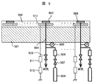
本発明の第2の実施例を図5を用いて説明する。図5は、本実施例のプラズマ処理装置
に係るウエハ載置用電極の構成の概略を示す縦断面図である。本図が実施例1と異なる点
を以下に説明する。図5は本発明の一実施例におけるウエハ載置用電極を示す。本実施例
のプラズマ処理装置に用いられるウエハ載置用電極111(以下、電極)は、電極の構造
体となる基材501,アルミナ製の溶射膜502,基材501の温度制御用装置(図示省
略)からなる。
A second embodiment of the present invention will be described with reference to FIG. FIG. 5 is a longitudinal sectional view schematically showing the configuration of the wafer mounting electrode according to the plasma processing apparatus of the present embodiment. Differences of this figure from the first embodiment will be described below. FIG. 5 shows a wafer mounting electrode in one embodiment of the present invention. A wafer mounting electrode 111 (hereinafter referred to as an electrode) used in the plasma processing apparatus of the present embodiment includes a
また電極表面には、ウエハ112と溶射膜502の間に伝熱用ガスを供給する複数の独
立した伝熱用ガス溝503が設けられる。設けられた複数の独立した伝熱用ガス溝503
には、それぞれに独立して伝熱用ガスを供給する配管504,ウエハ112と溶射膜502
間の圧力を計測する圧力計505,伝熱用ガスの供給量を制御するガス流量制御器506
,伝熱用ガスを供給するバルブ507,ガスボンベ508,伝熱用ガスの排気バルブ509
が接続される。
A plurality of independent heat
1 includes a
A
, A
Is connected.
プラズマ処理を行う場合は、バルブ507を開け、ガスボンベ508から伝熱用ガス
(本実施例ではヘリウムガス)を供給し、それぞれの伝熱用ガス溝503内のガス圧力を
圧力計505でモニタし、所望の圧力となるようガス流量制御器506を制御する。
When performing the plasma treatment, the
このように複数の独立した伝熱用ガス溝503により、ウエハ112と電極間の伝熱用
ガス圧をそれぞれの溝で個別に制御する場合、ウエハ112と電極間の熱伝達率をウエハ
面内で任意の分布にできる。複数の独立した伝熱用ガス溝503を設けることで、さらに
高精度にウエハ面内の熱伝導率を任意の分布に制御できるという効果がある。
As described above, when the heat transfer gas pressure between the
さらに本実施例では、電極表面に設けた複数の伝熱用ガス溝503にそれぞれ対応した
複数の独立した静電吸着用電極510を設ける。それぞれの静電吸着用電極510には、
高周波電力の伝送を遮断するフィルター511,静電吸着電極へ直流電圧を印加するため
の直流電源512が接続される。直流電源512から直流電圧を印加することで発生する
静電気力によりウエハ112を電極上へ吸着させることができる。またこの吸着力は印加
する直流電圧の大きさにより制御することができる。
Furthermore, in this embodiment, a plurality of independent
A
このように、溝部以外の接触部における電極表面とウエハ112間の接触熱伝達率を直
流電圧の大きさで制御することができ、ウエハ面内の接触熱通過率を任意の分布とするこ
とができる。溝部の伝熱用ガス圧の制御に加えて、さらに溝部に対応したウエハの接触部
での接触熱伝達率の制御を可能とすることで、ウエハ温度の制御範囲を大きくでき、高精
度にウエハ面内の温度分布を制御できるという効果がある。
As described above, the contact heat transfer coefficient between the electrode surface and the
上記実施例の変形例を図6を用いて説明する。図6は、図5に示す実施例の変形例に係
るウエハ載置用電極の構成の概略を示す縦断面図である。本図が実施例1,2と異なる点
を以下に説明する。
A modification of the above embodiment will be described with reference to FIG. FIG. 6 is a longitudinal sectional view schematically showing the configuration of the wafer mounting electrode according to a modification of the embodiment shown in FIG. Differences of this figure from the first and second embodiments will be described below.
プラズマ処理中のウエハ112の温度分布を検出する温度センサー601を設ける。温
度センサー601から得られたプラズマ処理中のウエハの温度が、あらかじめ決められた
温度分布となるようにガス流量制御器602のガス流量と直流電源603の出力電圧を制
御する。つまり、プラズマ処理中のウエハ温度の面内分布を測定し、得られた温度から、
伝熱用ガス圧の面内分布または各領域に印加する直流電圧を自動制御できるようにする。
これにより、高精度にウエハ面内の温度分布を制御できるという効果がある。
A
It is possible to automatically control the in-plane distribution of the gas pressure for heat transfer or the DC voltage applied to each region.
Thereby, there is an effect that the temperature distribution in the wafer surface can be controlled with high accuracy.
101…真空容器、102…シャワープレート、103…誘電体窓、104…処理室、
105…ガス供給装置、106…真空排気口、107…導波管、109…電磁波発生用電
源、110…磁場発生コイル、111…ウエハ載置用電極、112…ウエハ、113…マ
ッチング回路、114…高周波電源、201…基材、202…溶射膜、203…サセプタ
、204…第1の流路、205…第2の流路、206…第1の冷媒温調器、207…第2
の冷媒温調器、208…第1の伝熱用ガス溝、209…第2の伝熱用ガス溝、210…第
3の伝熱用ガス溝、211,212,504…配管、213,214,505…圧力計、
215,216…ガス流量制御器、217,218…バルブ、219,220…ガスボン
ベ、221,222…ガス排気バルブ、223…第1の静電吸着用電極、224…第2の
静電吸着用電極、225,226,511…フィルター、227,228,512,603
…直流電源、301,302,303…曲線、501…基材、502…溶射膜、503…
伝熱用ガス溝、506…ガス流量制御器、507…バルブ、508…ガスボンベ、509
…ガス排気バルブ、510…静電吸着用電極、601…温度センサー、602…ガス流量
制御器。
101 ... Vacuum vessel, 102 ... Shower plate, 103 ... Dielectric window, 104 ... Processing chamber,
DESCRIPTION OF
, 208, first heat transfer gas groove, 209, second heat transfer gas groove, 210, third heat transfer gas groove, 211, 212, 504, piping, 213, 214. , 505 ... Pressure gauge,
215, 216 ... Gas flow controllers, 217, 218 ... Valves, 219, 220 ... Gas cylinders, 221, 222 ... Gas exhaust valves, 223 ... First electrostatic adsorption electrode, 224 ... Second electrostatic adsorption electrode , 225, 226, 511 ... filter, 227, 228, 512, 603
... DC power supply, 301, 302, 303 ... curve, 501 ... substrate, 502 ... sprayed film, 503 ...
Gas groove for heat transfer, 506 ... Gas flow controller, 507 ... Valve, 508 ... Gas cylinder, 509
... gas exhaust valve, 510 ... electrostatic adsorption electrode, 601 ... temperature sensor, 602 ... gas flow rate controller.
Claims (5)
前記被処理材と前記電極の表面との間の空間の複数に分けられた領域各々に伝熱用のガスを供給しまたはこれらの領域から排気するとともに、前記電極表面に配置された膜の内部で前記表面を複数の領域に分けて配置された静電吸着用の複数の電極各々に直流電圧を印加して、前記被処理材の温度の分布を制御するプラズマ処理方法であって、
前記被処理材の温度を相対的に高くする領域に対応する位置に配置された前記静電吸着電極に印加する直流電圧をプラズマ処理中のこの被処理材のセルフバイアス電位と同電位となるように制御するとともに当該被処理材の領域に対応する位置に配置された前記被処理材と前記電極の表面との間の空間の領域での伝熱用のガスの圧力を低くすることを特徴とするプラズマ処理方法。 The inside of the processing chamber is depressurized by a vacuum exhaust device, gas is supplied into the processing chamber, plasma is generated in the processing chamber, and the material to be processed is adsorbed on the temperature-controlled electrode by electrostatic force. In a method of plasma processing a material,
Before SL while supplying a gas for heat transfer in each region which is divided into a plurality of spaces or exhaust from these regions between the surface of the electrode and the workpiece, the film disposed on the electrode surface A plasma processing method for controlling a temperature distribution of the material to be processed by applying a DC voltage to each of a plurality of electrodes for electrostatic attraction arranged inside the surface in a plurality of regions ,
A DC voltage applied to the electrostatic adsorption electrode disposed at a position corresponding to a region where the temperature of the material to be processed is relatively high is set to the same potential as the self-bias potential of the material to be processed during plasma processing. And reducing the pressure of the heat transfer gas in a space region between the material to be processed and the surface of the electrode disposed at a position corresponding to the region of the material to be processed. A plasma processing method.
Priority Applications (4)
| Application Number | Priority Date | Filing Date | Title |
|---|---|---|---|
| JP2006207341A JP4815298B2 (en) | 2006-07-31 | 2006-07-31 | Plasma processing method |
| US11/512,116 US20080023139A1 (en) | 2006-07-31 | 2006-08-30 | Plasma processing apparatus and plasma processing method |
| KR1020060082895A KR100839148B1 (en) | 2006-07-31 | 2006-08-30 | Plasma processing apparatus and plasma processing method |
| TW095132187A TW200807551A (en) | 2006-07-31 | 2006-08-31 | Apparatus and method for processing plasma |
Applications Claiming Priority (1)
| Application Number | Priority Date | Filing Date | Title |
|---|---|---|---|
| JP2006207341A JP4815298B2 (en) | 2006-07-31 | 2006-07-31 | Plasma processing method |
Publications (2)
| Publication Number | Publication Date |
|---|---|
| JP2008034669A JP2008034669A (en) | 2008-02-14 |
| JP4815298B2 true JP4815298B2 (en) | 2011-11-16 |
Family
ID=38984958
Family Applications (1)
| Application Number | Title | Priority Date | Filing Date |
|---|---|---|---|
| JP2006207341A Expired - Fee Related JP4815298B2 (en) | 2006-07-31 | 2006-07-31 | Plasma processing method |
Country Status (4)
| Country | Link |
|---|---|
| US (1) | US20080023139A1 (en) |
| JP (1) | JP4815298B2 (en) |
| KR (1) | KR100839148B1 (en) |
| TW (1) | TW200807551A (en) |
Families Citing this family (16)
| Publication number | Priority date | Publication date | Assignee | Title |
|---|---|---|---|---|
| US9338871B2 (en) * | 2010-01-29 | 2016-05-10 | Applied Materials, Inc. | Feedforward temperature control for plasma processing apparatus |
| US8916793B2 (en) | 2010-06-08 | 2014-12-23 | Applied Materials, Inc. | Temperature control in plasma processing apparatus using pulsed heat transfer fluid flow |
| US8880227B2 (en) | 2010-05-27 | 2014-11-04 | Applied Materials, Inc. | Component temperature control by coolant flow control and heater duty cycle control |
| JP5642531B2 (en) * | 2010-12-22 | 2014-12-17 | 東京エレクトロン株式会社 | Substrate processing apparatus and substrate processing method |
| US10274270B2 (en) | 2011-10-27 | 2019-04-30 | Applied Materials, Inc. | Dual zone common catch heat exchanger/chiller |
| JP5975755B2 (en) * | 2012-06-28 | 2016-08-23 | 株式会社日立ハイテクノロジーズ | Plasma processing apparatus and plasma processing method |
| JP6240441B2 (en) * | 2013-09-06 | 2017-11-29 | 株式会社日立ハイテクノロジーズ | Plasma processing equipment |
| KR102263827B1 (en) | 2014-03-21 | 2021-06-14 | 삼성디스플레이 주식회사 | Oxide semiconductor depositing apparatus and method of manufacturing oxide semiconductor using the same |
| JP6567943B2 (en) * | 2015-01-09 | 2019-08-28 | 株式会社日立ハイテクノロジーズ | Plasma processing apparatus and plasma processing method |
| US9779919B2 (en) | 2015-01-09 | 2017-10-03 | Hitachi High-Technologies Corporation | Plasma processing apparatus and plasma processing method |
| JP6877133B2 (en) * | 2016-03-28 | 2021-05-26 | 株式会社日立ハイテク | Plasma processing equipment and plasma processing method |
| CN108376659B (en) * | 2018-01-30 | 2020-08-04 | 上海华力微电子有限公司 | Helium pressure control system and method for static electricity removal of electrostatic chuck |
| JP7054642B2 (en) * | 2018-04-06 | 2022-04-14 | 東京エレクトロン株式会社 | Plasma processing equipment and plasma processing method |
| JP6931492B2 (en) * | 2018-12-21 | 2021-09-08 | Toto株式会社 | Electrostatic chuck |
| JP7486018B2 (en) * | 2018-12-21 | 2024-05-17 | Toto株式会社 | Electrostatic Chuck |
| US20220049350A1 (en) * | 2020-08-13 | 2022-02-17 | Applied Materials, Inc. | Apparatus design for photoresist deposition |
Family Cites Families (10)
| Publication number | Priority date | Publication date | Assignee | Title |
|---|---|---|---|---|
| US4692836A (en) * | 1983-10-31 | 1987-09-08 | Toshiba Kikai Kabushiki Kaisha | Electrostatic chucks |
| JPH07249586A (en) * | 1993-12-22 | 1995-09-26 | Tokyo Electron Ltd | Treatment device and its manufacturing method and method for treating body to be treated |
| JPH07335630A (en) * | 1994-06-13 | 1995-12-22 | Hitachi Ltd | Vacuum processing device |
| JP2880920B2 (en) * | 1994-10-27 | 1999-04-12 | 日本電気株式会社 | Etching equipment |
| US5880923A (en) * | 1997-06-09 | 1999-03-09 | Applied Materials Inc. | Method and apparatus for improved retention of a semiconductor wafer within a semiconductor wafer processing system |
| WO2000041229A1 (en) * | 1998-12-28 | 2000-07-13 | Tokyo Electron Limited | Plasma apparatus and lower electrode thereof |
| US6320736B1 (en) * | 1999-05-17 | 2001-11-20 | Applied Materials, Inc. | Chuck having pressurized zones of heat transfer gas |
| US20050230047A1 (en) * | 2000-08-11 | 2005-10-20 | Applied Materials, Inc. | Plasma immersion ion implantation apparatus |
| US7156951B1 (en) * | 2002-06-21 | 2007-01-02 | Lam Research Corporation | Multiple zone gas distribution apparatus for thermal control of semiconductor wafer |
| JP2005136025A (en) * | 2003-10-29 | 2005-05-26 | Trecenti Technologies Inc | Semiconductor manufacturing apparatus, method of manufacturing semiconductor device, and wafer stage |
-
2006
- 2006-07-31 JP JP2006207341A patent/JP4815298B2/en not_active Expired - Fee Related
- 2006-08-30 KR KR1020060082895A patent/KR100839148B1/en not_active IP Right Cessation
- 2006-08-30 US US11/512,116 patent/US20080023139A1/en not_active Abandoned
- 2006-08-31 TW TW095132187A patent/TW200807551A/en not_active IP Right Cessation
Also Published As
| Publication number | Publication date |
|---|---|
| TWI317150B (en) | 2009-11-11 |
| KR20080011626A (en) | 2008-02-05 |
| KR100839148B1 (en) | 2008-06-19 |
| JP2008034669A (en) | 2008-02-14 |
| US20080023139A1 (en) | 2008-01-31 |
| TW200807551A (en) | 2008-02-01 |
Similar Documents
| Publication | Publication Date | Title |
|---|---|---|
| JP4815298B2 (en) | Plasma processing method | |
| KR102430205B1 (en) | Plasma processing apparatus | |
| KR102455673B1 (en) | Focus ring and substrate processing apparatus | |
| US20100012274A1 (en) | Focus ring, substrate mounting table and plasma processing apparatus having same | |
| US20060207725A1 (en) | Substrate mounting table, substrate processing apparatus and substrate processing method | |
| KR102016408B1 (en) | Plasma processing apparatus | |
| US10964513B2 (en) | Plasma processing apparatus | |
| WO2010019196A2 (en) | Temperature controlled hot edge ring assembly | |
| JP5414172B2 (en) | Plasma processing apparatus and plasma processing method | |
| US20190244795A1 (en) | Plasma processing apparatus | |
| JP2006351887A (en) | Plasma processing device | |
| KR20200051494A (en) | Placing table, positioning method of edge ring and substrate processing apparatus | |
| US10615008B2 (en) | Temperature control method | |
| JP2011119708A (en) | Substrate holding device and plasma processing device | |
| JP2007067037A (en) | Vacuum processing device | |
| TWI794428B (en) | Workpiece placement apparatus and processing apparatus | |
| KR20170028849A (en) | Focus ring and substrate processing apparatus | |
| KR20220125205A (en) | Substrate support with increasing areal density and corresponding method of fabricating | |
| JP2012049376A (en) | Plasma processing apparatus and plasma processing method | |
| US9583314B2 (en) | Plasma processing apparatus | |
| JP2005079415A (en) | Plasma processing apparatus | |
| JP3950806B2 (en) | Plasma processing apparatus and plasma processing method | |
| KR20200051505A (en) | Placing table and substrate processing apparatus | |
| JP2010010231A (en) | Plasma treatment device | |
| JP2010267708A (en) | Device and method for vacuum processing |
Legal Events
| Date | Code | Title | Description |
|---|---|---|---|
| A621 | Written request for application examination |
Free format text: JAPANESE INTERMEDIATE CODE: A621 Effective date: 20090511 |
|
| A521 | Written amendment |
Free format text: JAPANESE INTERMEDIATE CODE: A523 Effective date: 20090511 |
|
| A977 | Report on retrieval |
Free format text: JAPANESE INTERMEDIATE CODE: A971007 Effective date: 20110330 |
|
| A131 | Notification of reasons for refusal |
Free format text: JAPANESE INTERMEDIATE CODE: A131 Effective date: 20110405 |
|
| A521 | Written amendment |
Free format text: JAPANESE INTERMEDIATE CODE: A523 Effective date: 20110603 |
|
| TRDD | Decision of grant or rejection written | ||
| A01 | Written decision to grant a patent or to grant a registration (utility model) |
Free format text: JAPANESE INTERMEDIATE CODE: A01 Effective date: 20110802 |
|
| A01 | Written decision to grant a patent or to grant a registration (utility model) |
Free format text: JAPANESE INTERMEDIATE CODE: A01 |
|
| A61 | First payment of annual fees (during grant procedure) |
Free format text: JAPANESE INTERMEDIATE CODE: A61 Effective date: 20110829 |
|
| R150 | Certificate of patent or registration of utility model |
Free format text: JAPANESE INTERMEDIATE CODE: R150 |
|
| FPAY | Renewal fee payment (event date is renewal date of database) |
Free format text: PAYMENT UNTIL: 20140902 Year of fee payment: 3 |
|
| LAPS | Cancellation because of no payment of annual fees |