JP4809648B2 - Manufacturing method of electronic device - Google Patents
Manufacturing method of electronic device Download PDFInfo
- Publication number
- JP4809648B2 JP4809648B2 JP2005254680A JP2005254680A JP4809648B2 JP 4809648 B2 JP4809648 B2 JP 4809648B2 JP 2005254680 A JP2005254680 A JP 2005254680A JP 2005254680 A JP2005254680 A JP 2005254680A JP 4809648 B2 JP4809648 B2 JP 4809648B2
- Authority
- JP
- Japan
- Prior art keywords
- inlet
- tape
- jig
- label
- mount
- Prior art date
- Legal status (The legal status is an assumption and is not a legal conclusion. Google has not performed a legal analysis and makes no representation as to the accuracy of the status listed.)
- Expired - Fee Related
Links
Images


Description
本発明は、電子装置の製造技術に関し、特に、非接触型電子タグ用インレットを用いた電子装置の製造工程に適用して有効な技術に関するものである。 The present invention relates to an electronic device manufacturing technique, and more particularly to a technique effective when applied to an electronic device manufacturing process using an inlet for a non-contact type electronic tag.
特開2002−53116号公報には、ライナレスラベルをロール状に保持する保持部と、単票RF−IDタグが載置されている載置台と、保持部から搬送されるライナレスラベルの糊面に載置部に載置されている単票RF−IDタグを貼り付ける貼り付け手段とを具備し、RF−IDタグを取り外しし易くしたRF−IDラベル作成機能付きプリンタが開示されている。 Japanese Patent Laid-Open No. 2002-53116 discloses a holding unit that holds a linerless label in a roll shape, a mounting table on which a cut sheet RF-ID tag is mounted, and a paste for a linerless label conveyed from the holding unit. There is disclosed a printer with an RF-ID label creating function that includes an attaching unit that attaches a single-sheet RF-ID tag placed on a placement unit to a surface and facilitates removal of the RF-ID tag. .
特表2003−523294号公報には、多様性を有し、安価な方法で幅広く様々な種類のRFIDラベル(裏付きまたはライナ無しのラベルを含む)を効果的に製造できるRFIDラベルの製造方法が開示されている。 Japanese Patent Publication No. 2003-523294 discloses a method of manufacturing an RFID label that can effectively manufacture a wide variety of types of RFID labels (including backed or unlined labels) by a variety of inexpensive methods. It is disclosed.
特開2003−256796号公報には、テープ状に加工した磁気式タグを、物品に取り付け可能な接着層を一表面に有し磁気式タグよりも面積の大きいラベル原紙の前記接着層面に取り付けることを特徴とする、面積を可及的に小さくした磁気式タグを含むラベルの製造方法が開示されている。
非接触型の電子タグは、半導体チップ内のメモリ回路に所望のデータを記憶させ、マイクロ波を使ってこのデータを読み取るようにしたタグであり、リードフレームで構成したアンテナに半導体チップを実装した構造を有している。 A non-contact type electronic tag is a tag in which desired data is stored in a memory circuit in a semiconductor chip, and this data is read using a microwave. A semiconductor chip is mounted on an antenna constituted by a lead frame. It has a structure.
電子タグは、半導体チップ内のメモリ回路にデータを記憶させるため、バーコードを利用したタグなどに比べて大容量のデータを記憶できる利点がある。また、メモリ回路に記憶させたデータは、バーコードに記憶させたデータに比べて不正な改竄が困難であるという利点もある。 Since the electronic tag stores data in a memory circuit in the semiconductor chip, there is an advantage that a large amount of data can be stored as compared with a tag using a barcode. In addition, the data stored in the memory circuit has an advantage that unauthorized tampering is difficult as compared with the data stored in the barcode.
ところで、紙ラベルシール型の電子タグは材料費が安価になることから、需要および普及が見込まれている。このような紙ラベルシール型の電子タグを製造するには、たとえばシール台紙上に等間隔で貼付された紙ラベルシールを1枚ずつ剥離し、剥離した紙ラベルシールの粘着面に個片化したインレットを貼付した後に、再び紙ラベルシールをシール台紙上の元の位置に貼り戻すといった作業が必要となる。このような作業を作業者の手作業で行う場合には、紙ラベルシールの粘着面に精度よくインレットを貼付することが困難になる課題が存在する。また、紙ラベルシールをシール台紙上の元の位置に貼り戻す際にも、精度よく紙ラベルシールを貼り直すことが困難になる課題が存在する。また、これら作業を手作業によって行うことにより、一連の作業時間が長大化してしまう課題が存在する。 By the way, the paper label seal type electronic tag is expected to be demanded and spread because the material cost is low. In order to manufacture such a paper label seal type electronic tag, for example, the paper label stickers affixed on the sticker board at regular intervals are peeled one by one, and separated into the adhesive surfaces of the peeled paper label stickers. After sticking the inlet, it is necessary to put the paper label sticker back to the original position on the sticker mount. When such an operation is performed manually by an operator, there is a problem that it is difficult to accurately apply the inlet to the adhesive surface of the paper label seal. In addition, there is a problem that it is difficult to reattach the paper label sticker with high accuracy when the paper label sticker is put back to the original position on the sticker mount. In addition, there is a problem that a series of work time is lengthened by performing these work manually.
本願に開示された1つの代表的な発明の1つの目的は、シール台紙から剥離した紙ラベルシールの粘着面に精度よくインレットを貼付できる技術を提供することにある。 One object of one representative invention disclosed in the present application is to provide a technique capable of accurately attaching an inlet to an adhesive surface of a paper label seal peeled from a sticker mount.
また、本願に開示された1つの代表的な発明の1つの目的は、シール台紙から剥離した紙ラベルシールの粘着面にインレットを貼付した後に、紙ラベルシールを精度よくシール台紙へ貼り戻せる技術を提供することにある。 In addition, one object of one representative invention disclosed in the present application is a technique that allows the paper label seal to be accurately attached to the seal mount after the inlet is applied to the adhesive surface of the paper label seal peeled from the seal mount. It is to provide.
また、本願に開示された1つの代表的な発明の1つの目的は、シール台紙から剥離した紙ラベルシールの粘着面にインレットを貼付し、再び紙ラベルシールをシール台紙へ貼り戻す一連の作業に要する時間を短縮化できる技術を提供することにある。 In addition, one object of one typical invention disclosed in the present application is to perform a series of operations of attaching an inlet to the adhesive surface of the paper label seal peeled off from the sticker mount and sticking the paper label seal back to the sticker mount again. The object is to provide a technique capable of shortening the time required.
本願において開示される発明のうち、代表的なものの概要を簡単に説明すれば、次のとおりである。 Of the inventions disclosed in the present application, the outline of typical ones will be briefly described as follows.
本発明による電子装置の製造方法は、以下の工程を含む:
(a)絶縁フィルムの主面に形成された導電性膜からなるアンテナと、前記アンテナの一部に形成され、一端が前記アンテナの外縁に延在するスリットと、複数のバンプ電極を介して前記アンテナに電気的に接続された半導体チップと、前記半導体チップを封止する樹脂とを備えた複数のインレットを用意する工程、
(b)連続テープ状の台紙と、前記台紙上に第1の間隔を隔てて連続して貼付され、前記台紙と対向している粘着面および前記粘着面とは反対側のラベル面を有する複数のラベルシールとを含む第1のテープを用意する工程、
(c)前記第1のテープを供給するテープ供給手段、第1の曲率半径の面取り部を有する剥離治具、インレット貼付台、前記ラベルシールの前記粘着面より弱い第1の粘着力を有し、前記第1の粘着力で個片化した前記インレットを保持し、保持した前記インレットを前記インレット貼付台上の定位置へ移すことのできるインレット貼付治具、および前記テープ供給手段から供給された前記第1のテープを収容するテープ収容手段を含む第1のユニットを用意し、前記テープ供給手段に前記第1のテープを取り付ける工程、
(d)前記台紙が前記剥離治具の前記面取り部と接し、前記剥離治具の前記面取り部を頂点として第1の角度を形成するように前記第1のテープを搬送し、前記剥離治具の前記面取り部にて前記複数のラベルシールのうちの1枚の一部を前記台紙から剥離して前記ラベル面を前記インレット貼付台と対向させつつ前記インレット貼付台上の第1の位置まで進め、前記第1のテープの搬送を停止する工程、
(e)1つの前記インレットを前記インレット貼付治具のインレット配置位置に配置し、前記インレット貼付治具によって前記1つのインレットを保持させる工程、
(f)前記(d)工程後、前記第1のテープの搬送が停止した状況下において前記インレット貼付治具を動作させ、前記インレット貼付治具に保持された前記1つのインレットを前記インレット貼付台上の前記1枚のラベルシールの前記粘着面へ貼付する工程、
(g)前記(f)工程後、前記第1のテープの搬送を再開し、前記第1のテープが前記剥離治具の前記面取り部を通過する際の復元力で、前記台紙から剥離していた前記1枚のラベルシールの前記一部を前記台紙に再貼付する工程、
(h)前記(d)〜(g)工程を繰り返す工程。
The method for manufacturing an electronic device according to the present invention includes the following steps:
(A) An antenna made of a conductive film formed on the main surface of the insulating film, a slit formed on a part of the antenna, one end extending to the outer edge of the antenna, and a plurality of bump electrodes Preparing a plurality of inlets including a semiconductor chip electrically connected to an antenna and a resin for sealing the semiconductor chip;
(B) a plurality of tapes having a continuous tape-like mount, an adhesive surface that is continuously affixed on the mount with a first interval, facing the mount, and a label surface opposite to the adhesive surface; A first tape including a label seal of
(C) Tape supply means for supplying the first tape, a peeling jig having a chamfered portion with a first radius of curvature, an inlet sticking base, and a first adhesive force weaker than the adhesive surface of the label seal. Supplied from the tape supply means and the inlet sticking jig capable of holding the inlet separated into pieces by the first adhesive force and moving the held inlet to a fixed position on the inlet sticking table. Preparing a first unit including a tape storage means for storing the first tape, and attaching the first tape to the tape supply means;
(D) The mount is in contact with the chamfered portion of the peeling jig, and the first tape is transported so as to form a first angle with the chamfered portion of the peeling jig as a vertex, and the peeling jig A part of one of the plurality of label seals is peeled off from the mount at the chamfered portion, and the label surface is opposed to the inlet sticking table and advanced to a first position on the inlet sticking table. A step of stopping the conveyance of the first tape;
(E) placing one inlet at the inlet placement position of the inlet sticking jig and holding the one inlet by the inlet sticking jig;
(F) After the step (d), the inlet sticking jig is operated in a state where the conveyance of the first tape is stopped, and the one inlet held by the inlet sticking jig is moved to the inlet sticking stand. A process of applying to the adhesive surface of the one label seal on the top,
(G) After the step (f), the conveyance of the first tape is resumed, and the first tape is peeled off from the mount with a restoring force when passing through the chamfered portion of the peeling jig. Reattaching the part of the one label sticker to the mount,
(H) A step of repeating the steps (d) to (g).
また、本発明による電子装置の製造方法は、以下の工程を含む:
(a)連続テープ状の絶縁フィルムの主面に形成された導電性膜からなるアンテナと、前記アンテナの一部に形成され、一端が前記アンテナの外縁に延在するスリットと、複数のバンプ電極を介して前記アンテナに電気的に接続された半導体チップと、前記半導体チップを封止する樹脂とを備えた複数のインレットを用意する工程、
(b)連続テープ状の台紙と、前記台紙上に第1の間隔を隔てて連続して貼付され、前記台紙と対向している粘着面および前記粘着面とは反対側のラベル面を有する複数のラベルシールとを含む第1のテープを用意する工程、
(c)前記第1のテープを供給するテープ供給手段、第1の曲率半径の面取り部を有する剥離治具、インレット貼付台、前記ラベルシールの前記粘着面より弱い第1の粘着力を有し、前記第1の粘着力で個片化した前記インレットを保持し、保持した前記インレットを前記インレット貼付台上の定位置へ移すことのできるインレット貼付治具、1つの前記インレットを前記インレット貼付治具上へ供給するインレット供給手段、前記絶縁フィルムを切断して前記インレット貼付治具上の前記1つのインレットを個片化する切断手段、および前記テープ供給手段から供給された前記第1のテープを収容するテープ収容手段を含む第1のユニットを用意し、前記テープ供給手段に前記第1のテープを取り付ける工程、
(d)前記台紙が前記剥離治具の前記面取り部と接し、前記剥離治具の前記面取り部を頂点として第1の角度を形成するように前記第1のテープを搬送し、前記剥離治具の前記面取り部にて前記複数のラベルシールのうちの1枚の一部を前記台紙から剥離して前記ラベル面を前記インレット貼付台と対向させつつ前記インレット貼付台上の第1の位置まで進め、前記第1のテープの搬送を停止する工程、
(e)前記インレット供給手段によって1つの前記インレットを前記インレット貼付治具のインレット配置位置まで供給した状況下において、前記切断手段によって前記絶縁フィルムを切断して前記インレット貼付治具上の前記1つのインレットを個片化し、前記インレット貼付治具によって前記1つのインレットを保持させる工程、
(f)前記(d)工程後、前記第1のテープの搬送が停止した状況下において前記インレット貼付治具を動作させ、前記インレット貼付治具に保持された前記1つのインレットを前記インレット貼付台上の前記1枚のラベルシールの前記粘着面へ貼付する工程、
(g)前記(f)工程後、前記第1のテープの搬送を再開し、前記第1のテープが前記剥離治具の前記面取り部を通過する際の復元力で、前記台紙から剥離していた前記1枚のラベルシールの前記一部を前記台紙に再貼付する工程、
(h)前記(d)〜(g)工程を繰り返す工程。
The method for manufacturing an electronic device according to the present invention includes the following steps:
(A) An antenna made of a conductive film formed on the main surface of a continuous tape-like insulating film, a slit formed on a part of the antenna, one end extending to the outer edge of the antenna, and a plurality of bump electrodes Preparing a plurality of inlets including a semiconductor chip electrically connected to the antenna via a resin and a resin for sealing the semiconductor chip;
(B) a plurality of tapes having a continuous tape-like mount, an adhesive surface that is continuously affixed on the mount with a first interval, facing the mount, and a label surface opposite to the adhesive surface; A first tape including a label seal of
(C) Tape supply means for supplying the first tape, a peeling jig having a chamfered portion with a first radius of curvature, an inlet sticking base, and a first adhesive force weaker than the adhesive surface of the label seal. An inlet sticking jig that holds the inlet separated into pieces by the first adhesive force and can move the held inlet to a fixed position on the inlet sticking table, and one inlet for the inlet sticking treatment. Inlet supply means for supplying onto the tool, cutting means for cutting the insulating film into pieces of the one inlet on the inlet sticking jig, and the first tape supplied from the tape supply means Preparing a first unit including a tape storage means for storing, and attaching the first tape to the tape supply means;
(D) The mount is in contact with the chamfered portion of the peeling jig, and the first tape is transported so as to form a first angle with the chamfered portion of the peeling jig as a vertex, and the peeling jig A part of one of the plurality of label seals is peeled off from the mount at the chamfered portion, and the label surface is opposed to the inlet sticking table and advanced to a first position on the inlet sticking table. A step of stopping the conveyance of the first tape;
(E) Under the situation where one inlet is supplied to the inlet placement position of the inlet sticking jig by the inlet feeding means, the insulating film is cut by the cutting means and the one on the inlet sticking jig is Dividing the inlet into pieces and holding the one inlet by the inlet attaching jig;
(F) After the step (d), the inlet sticking jig is operated in a state where the conveyance of the first tape is stopped, and the one inlet held by the inlet sticking jig is moved to the inlet sticking stand. A process of applying to the adhesive surface of the one label seal on the top,
(G) After the step (f), the conveyance of the first tape is resumed, and the first tape is peeled off from the mount with a restoring force when passing through the chamfered portion of the peeling jig. Reattaching the part of the one label sticker to the mount,
(H) A step of repeating the steps (d) to (g).
また、本願に開示されたその他の概要を項に分けて簡単に説明するとすれば、以下の通りである。
項1.第1のテープを供給するテープ供給手段、第1の曲率半径の面取り部を有する剥離治具、インレット貼付台、前記第1のテープに含まれるラベルシールの粘着面より弱い第1の粘着力を有し、前記第1の粘着力で個片化したインレットを保持し、保持した前記インレットを前記インレット貼付台上の定位置へ移すことのできるインレット貼付治具、および前記テープ供給手段から供給された前記第1のテープを収容するテープ収容手段を具備し、以下の工程を含む電子装置の製造方法にて用いる製造装置:
(a)絶縁フィルムの主面に形成された導電性膜からなるアンテナと、前記アンテナの一部に形成され、一端が前記アンテナの外縁に延在するスリットと、複数のバンプ電極を介して前記アンテナに電気的に接続された半導体チップと、前記半導体チップを封止する樹脂とを備えた複数の前記インレットを用意する工程、
(b)連続テープ状の台紙と、前記台紙上に第1の間隔を隔てて連続して貼付され、前記台紙と対向している前記粘着面および前記粘着面とは反対側のラベル面を有する複数の前記ラベルシールとを含む前記第1のテープを用意する工程、
(c)前記テープ供給手段に前記第1のテープを取り付ける工程、
(d)前記台紙が前記剥離治具の前記面取り部と接し、前記剥離治具の前記面取り部を頂点として第1の角度を形成するように前記第1のテープを搬送し、前記剥離治具の前記面取り部にて前記複数のラベルシールのうちの1枚の一部を前記台紙から剥離して前記ラベル面を前記インレット貼付台と対向させつつ前記インレット貼付台上の第1の位置まで進め、前記第1のテープの搬送を停止する工程、
(e)1つの前記インレットを前記インレット貼付治具のインレット配置位置に配置し、前記インレット貼付治具によって前記1つのインレットを保持させる工程、
(f)前記(d)工程後、前記第1のテープの搬送が停止した状況下において前記インレット貼付治具を動作させ、前記インレット貼付治具に保持された前記1つのインレットを前記インレット貼付台上の前記1枚のラベルシールの前記粘着面へ貼付する工程、
(g)前記(f)工程後、前記第1のテープの搬送を再開し、前記第1のテープが前記剥離治具の前記面取り部を通過する際の復元力で、前記台紙から剥離していた前記1枚のラベルシールの前記一部を前記台紙に再貼付する工程、
(h)前記(d)〜(g)工程を繰り返す工程。
項2.項1記載の製造装置において、
前記第1の角度は90°より小さい。
項3.項1記載の製造装置において、
前記剥離治具は、前記第1のテープと接する側面に前記面取り部が形成された平板、もしくは前記第1のテープと側面で接する円柱状治具である。
項4.項1記載の製造装置において、
前記テープ供給手段および前記収容手段は、前記第1のテープを巻き取って保持する。
項5.項1記載の製造装置において、
前記複数のラベルシールは紙を主成分とする。
項6.項1記載の製造装置において、
前記インレット貼付治具は、シリコンゴムを主成分とする。
項7.第1のテープを供給するテープ供給手段、第1の曲率半径の面取り部を有する剥離治具、インレット貼付台、前記第1のテープに含まれるラベルシールの粘着面より弱い第1の粘着力を有し、前記第1の粘着力で個片化したインレットを保持し、保持した前記インレットを前記インレット貼付台上の定位置へ移すことのできるインレット貼付治具、1つの前記インレットを前記インレット貼付治具上へ供給するインレット供給手段、絶縁フィルムを切断して前記インレット貼付治具上の前記1つのインレットを個片化する切断手段、および前記テープ供給手段から供給された前記第1のテープを収容するテープ収容手段を具備し、以下の工程を含む電子装置の製造方法にて用いる製造装置:
(a)連続テープ状の前記絶縁フィルムの主面に形成された導電性膜からなるアンテナと、前記アンテナの一部に形成され、一端が前記アンテナの外縁に延在するスリットと、複数のバンプ電極を介して前記アンテナに電気的に接続された半導体チップと、前記半導体チップを封止する樹脂とを備えた複数の前記インレットを用意する工程、
(b)連続テープ状の台紙と、前記台紙上に第1の間隔を隔てて連続して貼付され、前記台紙と対向している前記粘着面および前記粘着面とは反対側のラベル面を有する複数の前記ラベルシールとを含む前記第1のテープを用意する工程、
(c)前記テープ供給手段に前記第1のテープを取り付ける工程、
(d)前記台紙が前記剥離治具の前記面取り部と接し、前記剥離治具の前記面取り部を頂点として第1の角度を形成するように前記第1のテープを搬送し、前記剥離治具の前記面取り部にて前記複数のラベルシールのうちの1枚の一部を前記台紙から剥離して前記ラベル面を前記インレット貼付台と対向させつつ前記インレット貼付台上の第1の位置まで進め、前記第1のテープの搬送を停止する工程、
(e)前記インレット供給手段によって1つの前記インレットを前記インレット貼付治具のインレット配置位置まで供給した状況下において、前記切断手段によって前記絶縁フィルムを切断して前記インレット貼付治具上の前記1つのインレットを個片化し、前記インレット貼付治具によって前記1つのインレットを保持させる工程、
(f)前記(d)工程後、前記第1のテープの搬送が停止した状況下において前記インレット貼付治具を動作させ、前記インレット貼付治具に保持された前記1つのインレットを前記インレット貼付台上の前記1枚のラベルシールの前記粘着面へ貼付する工程、
(g)前記(f)工程後、前記第1のテープの搬送を再開し、前記第1のテープが前記剥離治具の前記面取り部を通過する際の復元力で、前記台紙から剥離していた前記1枚のラベルシールの前記一部を前記台紙に再貼付する工程、
(h)前記(d)〜(g)工程を繰り返す工程。
項8.項7記載の製造装置において、
前記第1の角度は90°より小さい。
項9.項7記載の製造装置において、
前記剥離治具は、前記第1のテープと接する側面に前記面取り部が形成された平板、もしくは前記第1のテープと側面で接する円柱状治具である。
項10.項7記載の製造装置において、
前記テープ供給手段および前記収容手段は、前記第1のテープを巻き取って保持する。
項11.項7記載の製造装置において、
前記複数のラベルシールは紙を主成分とする。
項12.項7記載の製造装置において、
前記インレット貼付治具は、シリコンゴムを主成分とする。
Further, other outlines disclosed in the present application will be briefly described as follows.
Item 1. A tape supply means for supplying a first tape, a peeling jig having a chamfered portion with a first radius of curvature, an inlet sticking base, and a first adhesive force weaker than an adhesive surface of a label seal included in the first tape. And an inlet sticking jig that holds the inlet separated by the first adhesive force and can move the held inlet to a fixed position on the inlet sticking table, and is supplied from the tape supply means. A manufacturing apparatus comprising a tape storage means for storing the first tape and used in a method for manufacturing an electronic device including the following steps:
(A) An antenna made of a conductive film formed on the main surface of the insulating film, a slit formed on a part of the antenna, one end extending to the outer edge of the antenna, and a plurality of bump electrodes Preparing a plurality of the inlets including a semiconductor chip electrically connected to an antenna and a resin for sealing the semiconductor chip;
(B) having a continuous tape-like mount, a sticking surface that is continuously affixed on the mount at a first interval, facing the mount, and a label surface opposite to the adhesive surface. Preparing the first tape including a plurality of the label seals;
(C) attaching the first tape to the tape supply means;
(D) The mount is in contact with the chamfered portion of the peeling jig, and the first tape is transported so as to form a first angle with the chamfered portion of the peeling jig as a vertex, and the peeling jig A part of one of the plurality of label seals is peeled off from the mount at the chamfered portion, and the label surface is opposed to the inlet sticking table and advanced to a first position on the inlet sticking table. A step of stopping the conveyance of the first tape;
(E) placing one inlet at the inlet placement position of the inlet sticking jig and holding the one inlet by the inlet sticking jig;
(F) After the step (d), the inlet sticking jig is operated in a state where the conveyance of the first tape is stopped, and the one inlet held by the inlet sticking jig is moved to the inlet sticking stand. A process of applying to the adhesive surface of the one label seal on the top,
(G) After the step (f), the conveyance of the first tape is resumed, and the first tape is peeled off from the mount with a restoring force when passing through the chamfered portion of the peeling jig. Reattaching the part of the one label sticker to the mount,
(H) A step of repeating the steps (d) to (g).
The first angle is less than 90 °.
The peeling jig is a flat plate in which the chamfered portion is formed on a side surface in contact with the first tape, or a cylindrical jig in contact with the first tape on the side surface.
Item 4. In the manufacturing apparatus according to Item 1,
The tape supply unit and the storage unit wind up and hold the first tape.
The plurality of label stickers are mainly composed of paper.
Item 6. In the manufacturing apparatus according to Item 1,
The inlet sticking jig contains silicon rubber as a main component.
(A) An antenna made of a conductive film formed on the main surface of the insulating film in the form of a continuous tape, a slit formed on a part of the antenna, one end extending to the outer edge of the antenna, and a plurality of bumps Preparing a plurality of the inlets including a semiconductor chip electrically connected to the antenna via an electrode and a resin for sealing the semiconductor chip;
(B) having a continuous tape-like mount, a sticking surface that is continuously affixed on the mount at a first interval, facing the mount, and a label surface opposite to the adhesive surface. Preparing the first tape including a plurality of the label seals;
(C) attaching the first tape to the tape supply means;
(D) The mount is in contact with the chamfered portion of the peeling jig, and the first tape is transported so as to form a first angle with the chamfered portion of the peeling jig as a vertex, and the peeling jig A part of one of the plurality of label seals is peeled off from the mount at the chamfered portion, and the label surface is opposed to the inlet sticking table and advanced to a first position on the inlet sticking table. A step of stopping the conveyance of the first tape;
(E) Under the situation where one inlet is supplied to the inlet placement position of the inlet sticking jig by the inlet feeding means, the insulating film is cut by the cutting means and the one on the inlet sticking jig is Dividing the inlet into pieces and holding the one inlet by the inlet attaching jig;
(F) After the step (d), the inlet sticking jig is operated in a state where the conveyance of the first tape is stopped, and the one inlet held by the inlet sticking jig is moved to the inlet sticking stand. A process of applying to the adhesive surface of the one label seal on the top,
(G) After the step (f), the conveyance of the first tape is resumed, and the first tape is peeled off from the mount with a restoring force when passing through the chamfered portion of the peeling jig. Reattaching the part of the one label sticker to the mount,
(H) A step of repeating the steps (d) to (g).
The first angle is less than 90 °.
The peeling jig is a flat plate in which the chamfered portion is formed on a side surface in contact with the first tape, or a cylindrical jig in contact with the first tape on the side surface.
The tape supply unit and the storage unit wind up and hold the first tape.
Item 11.
The plurality of label stickers are mainly composed of paper.
Item 12.
The inlet sticking jig contains silicon rubber as a main component.
本願において開示される発明のうち、1つの代表的なものによって得られる効果を簡単に説明すれば以下のとおりである。
(1)シール台紙から剥離した紙ラベルシールの粘着面に精度よく電子タグ用インレットを貼付することができる。
(2)シール台紙から剥離した紙ラベルシールの粘着面に電子タグ用インレットを貼付し、再び紙ラベルシールをシール台紙へ貼り戻す一連の作業に要する時間を短縮化することができる。
The effects obtained by one representative invention among the inventions disclosed in the present application will be briefly described as follows.
(1) The electronic tag inlet can be accurately attached to the adhesive surface of the paper label seal peeled from the seal mount.
(2) It is possible to reduce the time required for a series of operations of attaching the electronic tag inlet to the adhesive surface of the paper label seal peeled off from the sticker mount and attaching the paper label sticker to the seal mount again.
本願発明を詳細に説明する前に、本願における用語の意味を説明すると次の通りである。 Before describing the present invention in detail, the meaning of terms in the present application will be described as follows.
電子タグとは、RFID(Radio Frequency IDentification)システム、EPC(Electronic Product Code)システムの中心的電子部品であり、一般的に数mm以下(それ以上の場合を含む)のチップに電子情報、通信機能、データ書き換え機能を納めたものを言い、電波や電磁波で読み取り器と交信する。無線タグもしくはICタグとも呼ばれ、商品に取り付けることでバーコードよりも高度で複雑な情報処理が可能になる。アンテナ側(チップ外部または内部)からの非接触電力伝送技術により、電池を持たない半永久的に利用可能なタグも存在する。タグは、ラベル型、カード型、コイン型およびスティック型など様々な形状があり、用途に応じて選択する。通信距離は数mm程度のものから数mのものがあり、これも用途に応じて使い分けられる。 An electronic tag is a central electronic component of an RFID (Radio Frequency IDentification) system and an EPC (Electronic Product Code) system, and generally has electronic information and communication functions on a chip of several millimeters or less (including cases where it exceeds that). This means data rewriting function and communicates with the reader by radio waves or electromagnetic waves. It is also called a wireless tag or an IC tag, and by attaching it to a product, it is possible to perform information processing that is more sophisticated and complicated than a barcode. There is also a tag that can be used semi-permanently without a battery by a non-contact power transmission technology from the antenna side (outside or inside the chip). The tag has various shapes such as a label type, a card type, a coin type, and a stick type, and is selected according to the application. The communication distance ranges from several millimeters to several meters, and these are also properly used depending on the application.
インレット(一般にRFIDチップとアンテナとの複合体、ただし、アンテナのないものやアンテナをチップ上に集積したものもある。したがって、アンテナのないものもインレットに含まれることがある。)とは、金属コイル(アンテナ)にICチップを実装した状態での基本的な製品形態を言い、金属コイルおよびICチップは一般にむき出しの状態となるが、封止される場合もある。 An inlet (generally a composite of an RFID chip and an antenna, but there is also an antenna without an antenna or an antenna integrated on a chip. Therefore, an antenna without an antenna may also be included in the inlet). A basic product form in which an IC chip is mounted on a coil (antenna). The metal coil and the IC chip are generally exposed, but may be sealed.
以下の実施の形態においては便宜上その必要があるときは、複数のセクションまたは実施の形態に分割して説明するが、特に明示した場合を除き、それらはお互いに無関係なものではなく、一方は他方の一部または全部の変形例、詳細、補足説明等の関係にある。 In the following embodiments, when it is necessary for the sake of convenience, the description will be divided into a plurality of sections or embodiments. However, unless otherwise specified, they are not irrelevant to each other. There are some or all of the modifications, details, supplementary explanations, and the like.
また、以下の実施の形態において、要素の数等(個数、数値、量、範囲等を含む)に言及する場合、特に明示した場合および原理的に明らかに特定の数に限定される場合等を除き、その特定の数に限定されるものではなく、特定の数以上でも以下でも良い。 Further, in the following embodiments, when referring to the number of elements (including the number, numerical value, quantity, range, etc.), especially when clearly indicated and when clearly limited to a specific number in principle, etc. Except, it is not limited to the specific number, and may be more or less than the specific number.
さらに、以下の実施の形態において、その構成要素(要素ステップ等も含む)は、特に明示した場合および原理的に明らかに必須であると考えられる場合等を除き、必ずしも必須のものではないことは言うまでもない。また、実施例等において構成要素等について、「Aからなる」、「Aよりなる」と言うときは、特にその要素のみである旨明示した場合等を除き、それ以外の要素を排除するものでないことは言うまでもない。 Further, in the following embodiments, the constituent elements (including element steps and the like) are not necessarily indispensable unless otherwise specified and apparently essential in principle. Needless to say. In addition, when referring to the constituent elements in the embodiments, etc., “consisting of A” and “consisting of A” do not exclude other elements unless specifically stated that only the elements are included. Needless to say.
同様に、以下の実施の形態において、構成要素等の形状、位置関係等に言及するときは、特に明示した場合および原理的に明らかにそうでないと考えられる場合等を除き、実質的にその形状等に近似または類似するもの等を含むものとする。このことは、上記数値および範囲についても同様である。 Similarly, in the following embodiments, when referring to the shapes, positional relationships, etc. of the components, etc., the shapes are substantially the same unless otherwise specified, or otherwise apparent in principle. And the like are included. The same applies to the above numerical values and ranges.
また、本実施の形態を説明するための全図において同一機能を有するものは同一の符号を付し、その繰り返しの説明は省略する。 Also, components having the same function are denoted by the same reference symbols throughout the drawings for describing the embodiments, and the repetitive description thereof is omitted.
また、本実施の形態で用いる図面においては、平面図であっても図面を見易くするために部分的にハッチングを付す場合がある。 In the drawings used in the present embodiment, even a plan view may be partially hatched to make the drawings easy to see.
以下、本発明の実施の形態を図面に基づいて詳細に説明する。 Hereinafter, embodiments of the present invention will be described in detail with reference to the drawings.
(実施の形態1)
図1は、本実施の形態1の電子装置である電子タグ用インレットを示す平面図(表面側)、図2は、図1の一部を拡大して示す平面図、図3は、本実施の形態1の電子タグ用インレットを示す側面図、図4は、本実施の形態1の電子タグ用インレットを示す平面図(裏面側)、図5は、図4の一部を拡大して示す平面図である。上記したごとく、本実施の形態(実施例)の一部または全部は後続の実施の形態(実施例)の一部または全部である。したがって、重複する部分は原則として、説明を省略する。
(Embodiment 1)
FIG. 1 is a plan view (front side) showing an inlet for an electronic tag, which is an electronic device according to the first embodiment, FIG. 2 is a plan view showing a part of FIG. 1 in an enlarged manner, and FIG. 4 is a side view showing the electronic tag inlet of Embodiment 1, FIG. 4 is a plan view (back side) showing the electronic tag inlet of Embodiment 1, and FIG. 5 is an enlarged view of a part of FIG. It is a top view. As described above, part or all of the present embodiment (example) is part or all of the following embodiment (example). Therefore, in principle, the description of the overlapping parts is omitted.
本実施の形態1の電子タグ用インレット(以下、単にインレットという)1は、マイクロ波受信用のアンテナを備えた非接触型電子タグの主要部を構成するものである。このインレット1は、細長い長方形の絶縁フィルム2の一面に接着されたAl箔(導電性膜)からなるアンテナ3と、表面および側面がポッティング樹脂4で封止された状態でアンテナ3に接続されたチップ5とを備えている。絶縁フィルム2の一面(アンテナ3が形成された面)には、アンテナ3やチップ5を保護するためのカバーフィルム6が必要に応じてラミネートされる。
An electronic tag inlet (hereinafter simply referred to as an inlet) 1 according to the first embodiment constitutes a main part of a non-contact type electronic tag provided with an antenna for receiving microwaves. The inlet 1 is connected to the
上記絶縁フィルム2の長辺方向に沿ったアンテナ3の長さは、たとえば56mmであり、周波数2.45GHzのマイクロ波を効率よく受信できるように最適化されている。また、アンテナ3の幅は3mmであり、インレット1の小型化と強度の確保とが両立できるように最適化されている。
The length of the
アンテナ3のほぼ中央部には、その一端がアンテナ3の外縁に達する「L」字状のスリット7が形成されており、このスリット7の中途部には、ポッティング樹脂4で封止されたチップ5が実装されている。
An “L” -shaped
図6および図7は、上記スリット7が形成されたアンテナ3の中央部付近を拡大して示す平面図であり、図6はインレット1の表面側、図7は裏面側をそれぞれ示している。なお、これらの図では、チップ5を封止するポッティング樹脂4およびカバーフィルム6の図示は、省略してある。
6 and 7 are enlarged plan views showing the vicinity of the central portion of the
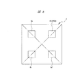
図示のように、スリット7の中途部には、絶縁フィルム2の一部を打ち抜いて形成したデバイスホール8が形成されており、前記チップ5は、このデバイスホール8の中央部に配置されている。デバイスホール8の寸法は、たとえば縦×横=0.8mm×0.8mmであり、チップ5の寸法は、縦×横=0.48mm×0.48mmである。
As shown in the figure, a
図6に示すように、チップ5の主面上には、たとえば4個のAu(金)バンプ9a、9b、9c、9dが形成されている。また、これらのAuバンプ9a、9b、9c、9dのそれぞれには、アンテナ3と一体に形成され、その一端がデバイスホール8の内側に延在するリード10が接続されている。
As shown in FIG. 6, on the main surface of the
上記4本のリード10のうち、2本のリード10は、スリット7によって2分割されたアンテナ3の一方からデバイスホール8の内側に延在し、チップ5のAuバンプ9a、9cと電気的に接続されている。また、残り2本のリード10は、アンテナ3の他方からデバイスホール8の内側に延在し、チップ5のAuバンプ9b、9dと電気的に接続されている。
Of the four leads 10, the two leads 10 extend from one of the
図8は、上記チップ5の主面に形成された4個のAuバンプ9a、9b、9c、9dのレイアウトを示す平面図、図9は、Auバンプ9aの近傍の拡大断面図、図10は、Auバンプ9cの近傍の拡大断面図、図11は、チップ5に形成された回路のブロック図である。
FIG. 8 is a plan view showing a layout of four
チップ5は、厚さ=0.15mm程度の単結晶シリコン基板からなり、その主面には、図11に示すような整流・送信、クロック抽出、セレクタ、カウンタ、ROMなどからなる回路が形成されている。ROMは、128ビットの記憶容量を有しており、バーコードなどの記憶媒体に比べて大容量のデータを記憶することができる。また、ROMに記憶させたデータは、バーコードに記憶させたデータに比べて不正な改竄が困難であるという利点がある。
The
上記回路が形成されたチップ5の主面上には、4個のAuバンプ9a、9b、9c、9dが形成されている。これら4個のAuバンプ9a、9b、9c、9dは、図8の二点鎖線で示す一対の仮想的な対角線上に位置し、かつこれらの対角線の交点(チップ5の主面の中心)からの距離がほぼ等しくなるようにレイアウトされている。これらのAuバンプ9a、9b、9c、9dは、たとえば電解めっき法を用いて形成されたもので、その高さは、たとえば15μm程度である。
Four Au bumps 9a, 9b, 9c, and 9d are formed on the main surface of the
なお、これらAuバンプ9a、9b、9c、9dのレイアウトは、図8に示したレイアウトに限られるものではないが、チップ接続時の加重に対してバランスを取りやすいレイアウトであることが好ましく、たとえば平面レイアウトにおいてAuバンプの接線によって形成される多角形が、チップの中心を囲む様に配置するのが好ましい。 Note that the layout of these Au bumps 9a, 9b, 9c, and 9d is not limited to the layout shown in FIG. 8, but is preferably a layout that can easily balance the weight at the time of chip connection. It is preferable that the polygon formed by the tangent line of the Au bump in the planar layout is arranged so as to surround the center of the chip.
上記4個のAuバンプ9a、9b、9c、9dのうち、たとえばAuバンプ9aは、前記図11に示す回路の入力端子を構成し、Auバンプ9bは、GND端子を構成している。また、残り2個のAuバンプ9c、9dは、上記回路には接続されていないダミーのバンプを構成している。
Of the four
図9に示すように、回路の入力端子を構成するAuバンプ9aは、チップ5の主面を覆うパッシベーション膜20とポリイミド樹脂21とをエッチングして露出させた最上層メタル配線22の上に形成されている。また、Auバンプ9aと最上層メタル配線22との間には、両者の密着力を高めるためのバリアメタル膜23が形成されている。パッシベーション膜20は、たとえば酸化シリコン膜と窒化シリコン膜との積層膜で構成され、最上層メタル配線22は、たとえばAl合金膜で構成されている。また、バリアメタル膜23は、たとえばAl合金膜に対する密着力が高いTi膜と、Auバンプ9aに対する密着力が高いPd膜との積層膜で構成されている。図示は省略するが、回路のGND端子を構成するAuバンプ9bと最上層メタル配線22との接続部も、上記と同様の構成になっている。一方、図10に示すように、ダミーのバンプを構成するAuバンプ9c(および9d)は、上記最上層メタル配線22と同一配線層に形成されたメタル層24に接続されているが、このメタル層24は、前記回路に接続されていない。
As shown in FIG. 9, the
このように、本実施の形態1のインレット1は、絶縁フィルム2の一面に形成したアンテナ3の一部に、その一端がアンテナ3の外縁に達するスリット7を設け、このスリット7によって2分割されたアンテナ3の一方にチップ5の入力端子(Auバンプ9a)を接続し、他方にチップ5のGND端子(Auバンプ9b)を接続する。この構成により、アンテナ3の実効的な長さを長くすることができるので、必要なアンテナ長を確保しつつ、インレット1の小型化を図ることができる。
As described above, the inlet 1 according to the first embodiment is provided with a
また、本実施の形態1のインレット1は、チップ5の主面上に、回路の端子を構成するAuバンプ9a、9bとダミーのAuバンプ9c、9dとを設け、これら4個のAuバンプ9a、9b、9c、9dをアンテナ3のリード10に接続する。この構成により、回路に接続された2個のAuバンプ9a、9bのみをリード10に接続する場合に比べて、Auバンプとリード10の実効的な接触面積が大きくなるので、Auバンプとリード10の接着強度、すなわち両者の接続信頼性が向上する。また、4個のAuバンプ9a、9b、9c、9dを図8に示したようなレイアウトでチップ5の主面上に配置することにより、Auバンプ9a、9b、9c、9dにリード10を接続した際に、チップ5が絶縁フィルム2に対して傾くことがない。これにより、チップ5をポッティング樹脂4で確実に封止することができるので、インレット1の製造歩留まりが向上する。
Further, the inlet 1 of the first embodiment is provided with Au bumps 9a and 9b and dummy Au bumps 9c and 9d constituting circuit terminals on the main surface of the
次に、上記のように構成されたインレット1の製造方法を図12〜図21を用いて説明する。図12は、インレット1の製造工程を説明するフローチャートである。 Next, the manufacturing method of the inlet 1 comprised as mentioned above is demonstrated using FIGS. FIG. 12 is a flowchart for explaining the manufacturing process of the inlet 1.
まず、ウエハ状の半導体基板(以下、単に基板と記す)の主面上に半導体素子、集積回路および上記バンプ電極9a〜9dなどを形成するウエハ処理を実施する(工程P1)。続いて、そのウエハ状の基板をダイシングによりチップ単位に分割し、前述のチップ5を形成する(工程P2)。
First, wafer processing for forming a semiconductor element, an integrated circuit, the
図13は、インレット1の製造に用いる絶縁フィルム2を示す平面図、図14は、図13の一部を拡大して示す平面図である。
FIG. 13 is a plan view showing the insulating
図13に示すように、連続テープ状の絶縁フィルム2は、リール25に巻き取られた状態でインレット1の製造工程に搬入される。この絶縁フィルム2の一面には、あらかじめ多数のアンテナ3が所定の間隔で形成されている。これらのアンテナ3を形成するには、たとえば絶縁フィルム2の一面に厚さ20μm程度のAl箔を接着し、このAl箔をアンテナ3の形状にエッチングする。このとき、それぞれのアンテナ3に、前述したスリット7およびリード10を形成する。絶縁フィルム2は、フィルムキャリアテープの規格に従ったもので、たとえば幅50mmまたは70mm、厚さ25μmのポリエチレンナフタレート製フィルムからなる。このように、アンテナ3をAl箔から形成し、絶縁フィルム2をポリエチレンナフタレートから形成することにより、たとえばアンテナ3をCu箔から形成し、絶縁フィルム2をポリイミド樹脂から形成した場合に比べてインレット1の材料コストを低減することができる。
As shown in FIG. 13, the continuous tape-like
次いで、アンテナ3のチップ5が搭載される面にインレット1の製品番号等の品種を識別するための識別マークを付与する。この識別マークは、たとえばレーザーを用いた刻印方法等によって形成することができる。
Next, an identification mark for identifying the product type such as the product number of the inlet 1 is provided on the surface of the
次に、図15に示すように、ボンディングステージ31とボンディングツール32とを備えたインナーリードボンダ30にリール25を装着し、ボンディングステージ31の上面に沿って絶縁フィルム2を移動させながら、アンテナ3にチップ5を接続する(工程P3)。
Next, as illustrated in FIG. 15, the
絶縁フィルム2を移動させている駆動ローラーKRL1は、寸法および回転速度等の動作が同じ規格のものを2つ一組で用いるものであり、2つの駆動ローラーKRL1が絶縁フィルム2を挟み、摩擦力で絶縁フィルム2を移動させるものである。また、図15中に示した4つの駆動ローラーKRL1は、すべて同じ規格のものである。絶縁フィルム2を移動させるに当たり、このような方式を適用することにより、薄い絶縁フィルム2でも対応でき、絶縁フィルム2へのダメージが少なく、絶縁フィルム2を高速搬送することができる。また、駆動ローラーKRL1は、図15中には示していないパルスモーターから動力を得て動作する。
The driving roller KRL1 that moves the insulating
アンテナ3にチップ5を接続するには、図16(図15の要部拡大図)に示すように、80℃程度に加熱したボンディングステージ31の上にチップ5を搭載し、このチップ5の真上に絶縁フィルム2のデバイスホール8を位置決めした後、デバイスホール8の内側に突出したリード10の上面に350℃程度に加熱したボンディングツール32を押し当て、Auバンプ(9a〜9d)とリード10を接触させる。この時、ボンディングツール32に所定の超音波および荷重を0.2秒程度印加することにより、リード10とAuバンプ(9a〜9d)との界面にAu/Al接合が形成され、Auバンプ(9a〜9d)とリード10が互いに接着する。
In order to connect the
次に、ボンディングステージ31の上に新たなチップ5を搭載し、続いて絶縁フィルム2をアンテナ3の1ピッチ分だけ移動させた後、上記と同様の操作を行うことによって、このチップ5をアンテナ3に接続する。以後、上記と同様の操作を繰り返すことによって、絶縁フィルム2に形成された全てのアンテナ3にチップ5を接続する。チップ5とアンテナ3の接続作業が完了した絶縁フィルム2は、リール25に巻き取られた状態で次の樹脂封止工程に搬送される。
Next, a
なお、Auバンプ(9a〜9d)とリード10の接続信頼性を向上させるためには、図17に示すように、4本のリード10をアンテナ3の長辺方向と直交する方向に延在させた方がよい。図18に示すように、4本のリード10をアンテナ3の長辺方向と平行に延在させた場合は、完成したインレット1を折り曲げたときに、Auバンプ(9a〜9d)とリード10の接合部に強い引っ張り応力が働くので、両者の接続信頼性が低下する虞がある。
In order to improve the connection reliability between the Au bumps (9a to 9d) and the
チップ5の樹脂封止工程では、図19および図20に示すように、ディスペンサ33などを使ってデバイスホール8の内側に実装されたチップ5の上面および側面にポッティング樹脂4を供給する(工程P4)。
In the resin sealing process of the
次いで、組立一貫機KIK内に設けられた加熱炉内において、ポッティング樹脂4に対して約120℃で仮ベーク処理を施す(工程P5)。図示は省略するが、この樹脂封止工程においても、絶縁フィルム2を移動させながら、ポッティング樹脂4の供給および仮ベーク処理を行う。ポッティング樹脂4の供給および仮ベーク処理が完了した絶縁フィルム2は、図21に示すように、リール25に巻き取られた状態で次のベーク処理が行われる加熱炉KNRへ搬送され、約120℃でベーク処理が施される(工程P6)。
Next, a temporary baking process is performed on the potting resin 4 at about 120 ° C. in a heating furnace provided in the integrated assembly machine KIK (process P5). Although illustration is omitted, also in this resin sealing step, the potting resin 4 is supplied and provisional baking is performed while moving the insulating
上記ベーク処理が完了した絶縁フィルム2は、リール25に巻き取られた状態で次工程へ搬送される。ここでは、アンテナ3にチップ5が搭載されチップ5がポッティング樹脂4によって封止されてなる構造体に対して抜取外観検査を行う。ここでは、すべての構造体に対して外観検査を行うのではなく、無作為抽出した所定数の構造体に対して外観検査を行う(工程P7)。すなわち、外観不良が見つかった場合には、外観不良の発生具合から工程P6までに用いた製造装置および材料等で、インレット1の製造に当たって不具合のある個所を特定し、以降のインレット1の製造へフィードバックすることによって不具合の発生を未然に防ぐためのものである。また、ここで言う外観不良とは、構造体への異物の付着、構造体に生じた傷、ポッティング樹脂4の封止不良(ぬれ不足)、チップ5の欠け等の破損、構造体の好ましくない変形、アンテナ3に形成(刻印)された前述の識別マークの認識不良のうちの1つ以上を含むものである。
The insulating
次いで、顧客からの要求がある場合には、絶縁フィルム2の両側部に図22に示すような絶縁フィルム2を搬送するためのスプロケットホール36を所定の間隔で形成する(工程P8)。スプロケットホール36は、絶縁フィルム2の一部をパンチで打ち抜くことによって形成することができる。一方、このようなスプロケットホール36を形成しない場合には、スプロケットホール36の形成に要するコスト(絶縁フィルム2の両端のスプロケットホール36を一組(2個)形成するのに約1円)を削減することができる。
Next, when there is a request from a customer, sprocket holes 36 for conveying the insulating
次いで、インレット1となる上記構造体の各々に対して通信特性検査(工程P9)、ポッティング樹脂4(図20参照)の外観検査(工程P10)、アンテナ3に付与された識別マークの外観検査(工程P11)、および工程P10、P11を経た上での良品選別(工程P12)を順次行う。 Next, for each of the structures to be the inlet 1, a communication characteristic inspection (process P9), an appearance inspection of the potting resin 4 (see FIG. 20) (process P10), and an appearance inspection of the identification mark given to the antenna 3 (step P10). The non-defective product selection (process P12) is performed sequentially after the process P11) and the processes P10 and P11.
次いで、最終的な良品および不良品の上記構造体数をそれぞれ調べる(工程P14)。続いて、リール25に巻き取られた絶縁フィルム2の梱包および払い出しが行われ(工程P15)、その後顧客側へ出荷される(工程P16)。この場合、顧客側で絶縁フィルム2をアンテナ3間で切断することにより個々のインレット1を得ることができる。また、顧客の要求に応じて、製造側(出荷側)で個々のインレット1に切断した状態で出荷してもよい。なお、絶縁フィルム2の梱包および払い出し後、所定数の絶縁フィルム2を無作為抽出し、工程P9と同様の通信特性検査を行ってもよい。
Next, the number of the above-mentioned structures of the final non-defective product and the defective product is examined (step P14). Subsequently, the insulating
次に、上記のようにして製造したインレット1を電子タグへ組み込む工程について説明する。本実施の形態1の電子タグは、たとえばラベルシール型であり、物品の表面に貼付して用いることで商品管理等を行えるようにしたものである。 Next, a process for incorporating the inlet 1 manufactured as described above into an electronic tag will be described. The electronic tag according to the first embodiment is, for example, a label seal type, and can be used for product management and the like by being attached to the surface of an article.
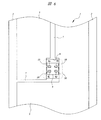
図23、図24および図25は、本実施の形態1の電子タグの製造に用いるラベルシールのそれぞれ要部斜視図、要部側面図および要部平面図である。図23〜図25に示すように、本実施の形態1の紙製のラベルシール41は、一般強粘着タイプのラベルシールであり、種々の印刷等が施されるラベル面およびそのラベル面とは反対側の粘着面を有し、連続テープ状の台紙42に一定の間隔(第1の間隔)を隔てて連続して貼付され、その台紙42が芯部43に巻き取られた状態のラベルテープ(第1のテープ)LTとして供給される。このようなラベルテープLTを図26〜図28に示すような作業ユニット(第1のユニット)に取り付ける。この作業ユニットは、テープ供給リール(テープ供給手段)45、貼付ステージ(インレット貼付台)46、回転板(インレット貼付治具)47、ラベル剥離板(剥離治具)48、ガイド軸49およびテープ巻き取りリール(テープ収容手段)50等から形成されている。また、蝶番51を介して貼付ステージ46と回転板47とが連結され、固定された貼付ステージ46に向かって回転板47が回転動作する構造となっている。回転板47は、たとえば約1mmの厚さでインレット1とほぼ同じ平面外形を有するシリコンゴムから形成されたインレット保持具(インレット配置位置)52を備え、前述の回転運動によってこのインレット保持具52が貼付ステージ46の所定の位置に接触する。また、たとえばテープ巻き取りリール50と連結したハンドル(図示は省略)を操作することにより、ラベルシール41が貼付された台紙42をテープ供給リール45から引き出し、テープ巻き取りリール50に巻き取ることができる。
23, 24, and 25 are a perspective view, a side view, and a plan view, respectively, of main parts of a label seal used for manufacturing the electronic tag according to the first embodiment. As shown in FIGS. 23 to 25, the paper-made
ラベルシール41が貼付された台紙42は、貼付ステージ46とラベルシール41とが対向するようにテープ供給リール45から引き出され、貼付ステージ46上の所定の位置で台紙42のラベルシール41が貼付されていない面と接するラベル剥離板48によって鋭角的(前記面取り部を頂点として第1の角度を形成するように)に搬送軌道を変えられる。ラベル剥離板48の台紙42と接する部分は、所定の曲率半径(第1の曲率半径)の面取り加工が施された面取り部となっている。その後、台紙42は、台紙42のラベルシール41が貼付されていない面と接するガイド軸49によって搬送軌道をガイドされてテープ巻き取りリール50に巻き取られる。ここで本発明者らは、ラベル剥離板48によって台紙42の搬送軌道が変えられる際に、以下のような現象が起こることを見出した。すなわち、その搬送軌道が変わる場所でラベルシール41の貼付ステージ46へ向かっての剥離が始まり(図27参照)、ラベルシール41の終端部がその搬送軌道が変わる場所を通過する時にラベルシール41は完全に剥離せず、復元力が作用して貼付ステージ46から起き上がるようにして台紙42の元々貼付されていた場所へ戻り(図28参照)、再び台紙42に貼付されるものである。
The
そこで本実施の形態1では、上記の現象を利用し、ラベルシール41が台紙42から剥離している際に現れるラベルシール41の粘着面に位置精度よくインレット1を貼付するものである。また、図29に示すように、本実施の形態1において、ラベルシール41は台紙42の搬送方向での幅W1および幅W1と交差する方向での幅W2が20mm〜300mm程度であり、厚さが粘着面の接着剤も含んで50〜100μm程度であり、隣接するラベルシール41間の間隔D1は3〜5mm程度であり、台紙42の厚さが30〜80μm程度である。なお、ラベルシール41の粘着面は、ラベルシール41が台紙42に貼付されている時には台紙と対向している。また、ラベル剥離板48の台紙42と接する部分に施された面取り加工は、曲率半径が1mm〜5mm程度、好ましくは約1.5mmのものであり、ラベルシール41が薄くなるのに合わせて小さくする。
Therefore, in the first embodiment, the above phenomenon is used, and the inlet 1 is attached to the adhesive surface of the
まず、インレット保持具52上に平面外形を合わせて1つのインレット1を配置する(図26参照)。配置されたインレット1は、インレット保持具52自体が有する粘着力によってインレット保持具52に保持される。このインレット保持具52の粘着力(第1の粘着力)は、ラベルシール41の粘着面に塗布されている接着剤の粘着力より弱いものである。
First, one inlet 1 is arranged on the
次に、テープ巻き取りリール50と連結したハンドルを操作し、台紙42をテープ供給リール45から引き出し、ラベル剥離板48によって台紙42の搬送軌道が変わる場所にてラベルシール41を貼付ステージ46上へ剥離させていく。次いで、剥離し始めたラベルシール41の先端が貼付ステージ46の表面に付与してある合わせ位置印(第1の位置)CPに達したら台紙41の引き出しを停止する。次いで、その状況下で回転板47を回転させ、インレット保持具52に保持されているインレット1をラベルシール41の粘着面に押し付ける。次いで、回転板47を逆方向へ回転させて元の位置へ戻す。前述したように、インレット保持具52の粘着力は、ラベルシール41の粘着面に塗布されている接着剤の粘着力より弱いことから、回転板47を元の位置へ戻した際に、インレット1は、インレット保持具52からラベルシール41の粘着面へ移し取られる(図27参照)。このようにしてインレット1をラベルシール41の粘着面へ貼付することにより、その粘着面内における所定位置にインレット1を精度よく、かつ効率よく貼付することが可能となる。
Next, the handle connected to the tape take-
続いて、テープ巻き取りリール50と連結したハンドルを操作してテープ巻き取りリール50による台紙42の巻き取り(テープ供給リール45からの台紙42の引き出し)を再開する。それにより、台紙42から一部が剥離して貼付ステージ46へ引き出され、インレット1が粘着面に貼付されたラベルシール41は、終端部がラベル剥離板48によって台紙42の搬送軌道が変わる場所まで達したところで、復元力が作用して貼付ステージ46から起き上がるようにして台紙42の元々貼付されていた場所へ戻って再び台紙42に貼付され、台紙42ごとテープ巻き取りリール50に巻き取られる(図28および図29参照)。本実施の形態1では、このラベルシール41の台紙42からの剥離から再貼付までの一連の作業を、1枚のラベルシール41につき0.5秒〜1.0秒程度の速さで行うことが好ましい。それにより、ラベルシール41を台紙42の元々貼付されていた場所へ貼り戻す際にも、容易に正確な位置精度で貼り戻すことが可能となる。その結果、ラベルシール41にインレット1を貼付する一連の作業に要する時間を短縮化することができる。また、ラベルシール41の大きさが変わっても、同様の工程を容易に適用することができるので、様々な大きさのラベルシール41に対して短時間かつ低価格でインレット1を貼付する一連の作業を実施することができる。
Subsequently, the handle connected to the tape take-
上記の一連の作業をテープ供給リール45から引き出されるラベルシール41のすべてに対して実施することで、ラベルシール41へのインレット1の貼付作業を行う。ラベルシール41が再び台紙42へ貼付された後には、インレット1はラベルシール41と台紙42との間に位置し、ラベルシール41および台紙42に周囲を覆われることになる。
By performing the above-described series of operations on all of the label seals 41 pulled out from the
上記の実施の形態1では、ラベルシール41にインレット1を貼付するのに用いる作業ユニットにおいて、台紙42と接する部分で所定の曲率半径の面取り加工が施されたラベル剥離板48を配置した場合について説明したが、図30に示すように、ラベル剥離板48の代わりに、断面が前述の曲率半径の値と同程度の値の半径を有する円形の円柱状のシャフト(円柱状治具)48Aを配置してもよい。
In the first embodiment described above, in the work unit used to attach the inlet 1 to the
(実施の形態2)
前記実施の形態1では、ラベルシール41にインレット1を貼付する際には、すでに個片化されているインレット1を用い、1個ずつインレット保持具52上に配置しつつ貼付作業を行う場合について説明したが(図26〜図28参照)、本実施の形態2は、インレット1を個片化する工程から個片化したインレット1をラベルシール41に貼付する工程までの一連の作業を自動化したものである。
(Embodiment 2)
In the first embodiment, when the inlet 1 is pasted on the
図31は、本実施の形態2において上記の一連の作業を行う作業ユニットの説明図である。本実施の形態2におけるその作業ユニットは、前記実施の形態1で図26〜図28を用いて説明した作業ユニットの構成に、インレット搬送ユニット(インレット供給手段)61、CCD(Charge Coupled Device)カメラ62および金型(切断手段)63等を加えたものである。また、インレット保持具52は、インレット1を真空吸着するインレット吸着手段を有し、インレット保持具52自体が有する粘着力だけでなく、そのインレット吸着手段の吸引力も用いてインレット1を保持する構造となっている。
FIG. 31 is an explanatory diagram of a work unit that performs the above-described series of work in the second embodiment. The working unit according to the second embodiment includes an inlet transport unit (inlet supply means) 61, a CCD (Charge Coupled Device) camera in the construction of the working unit described in the first embodiment with reference to FIGS. 62, a mold (cutting means) 63 and the like are added. The
まず、インレット1となる複数の構造体が形成されたテープ状の絶縁フィルム2をインレット搬送ユニット61にセットする。次いで、インレット搬送ユニット61によって絶縁フィルム2を搬送し、CCDカメラ62による画像処理によって絶縁フィルム2の切断位置を確認したら絶縁フィルム2の搬送を停止する。次いで、インレット保持具52のインレット吸着手段が1つのインレット1に相当する絶縁フィルム2を真空吸着し、インレット保持具52の粘着力も用いてその1つのインレット1に相当する絶縁フィルム2を保持する。次いで、インレット保持具52がその1つのインレット1に相当する絶縁フィルム2を保持した状況下で金型63を操作し、前記切断位置にて絶縁フィルム2を切断し、1つのインレット1を個片化する。個片化されたインレット1は、個片化と同時に自動的にインレット保持具52に移し取ることができる。インレット1を個片化した後は、前記実施の形態1において図27および図28を用いて説明した工程と同様に、回転板47を操作してラベルシール41の粘着面にインレット1を貼付し、ラベルシール41を台紙42ごとテープ巻き取りリール50に巻き取っていく。なお、インレット1をラベルシール41の粘着面に貼付した後で前記インレット吸着手段による真空吸着は解除する。このインレット1の個片化からインレット1のラベルシール41への貼付の一連の作業をテープ供給リール45から引き出されるラベルシール41のすべてに対して実施することで、ラベルシール41へのインレット1の貼付作業を行う。
First, the tape-like
上記の本実施の形態2によれば、前記実施の形態1で説明したラベルシール41にインレット1を貼付する作業ユニットにインレット1を個片化するユニット(インレット搬送ユニット61、CCDカメラ62および金型63等)を加えたことにより、たとえば個片化したインレット1をインレット保持具52上に配置する作業等を自動作業で行うことが可能となり、作業者の手作業を廃止することができる。それにより、前記実施の形態1よりもさらに正確な位置精度でインレット1をインレット保持具52上に配置することができる。また、種々の作業を自動化したことにより、ラベルシール41にインレット1を貼付する一連の作業に要する時間を前記実施の形態1よりも短縮化することができる。
According to the above-described second embodiment, the unit (
上記の本実施の形態2によっても前記実施の形態1と同様の効果を得ることができる。 According to the second embodiment described above, the same effect as in the first embodiment can be obtained.
以上、本発明者によってなされた発明を実施の形態に基づき具体的に説明したが、本発明は前記実施の形態に限定されるものではなく、その要旨を逸脱しない範囲で種々変更可能であることはいうまでもない。 As mentioned above, the invention made by the present inventor has been specifically described based on the embodiment. However, the present invention is not limited to the embodiment, and various modifications can be made without departing from the scope of the invention. Needless to say.
たとえば、前記実施の形態では、紙製のラベルシールを用いて電子タグを製造する場合について説明したが、紙製のラベルシールの代わりに樹脂フィルム製のラベルシールを用いてもよい。 For example, in the above embodiment, the case where an electronic tag is manufactured using a paper label seal has been described. However, a resin film label seal may be used instead of a paper label seal.
本発明の電子装置の製造方法は、たとえば個片化された電子タグ用インレットをラベルシールの粘着面に貼付する工程にて適用することができる。 The method for manufacturing an electronic device of the present invention can be applied, for example, in a process of attaching individualized electronic tag inlets to an adhesive surface of a label seal.
1 インレット
2 絶縁フィルム
3 アンテナ
4 ポッティング樹脂
5 チップ
6 カバーフィルム
7 スリット
8 デバイスホール
9a、9b、9c、9d Auバンプ
10 リード
20 パッシベーション膜
21 ポリイミド樹脂
22 最上層メタル配線
23 バリアメタル膜
24 メタル層
25 リール
30 インナーリードボンダ
31 ボンディングステージ
32 ボンディングツール
33 ディスペンサ
36 スプロケットホール
41 ラベルシール
42 台紙
43 芯部
45 テープ供給リール(テープ供給手段)
46 貼付ステージ(インレット貼付台)
47 回転板(インレット貼付治具)
48 ラベル剥離板(剥離治具)
48A シャフト(円柱状治具)
49 ガイド軸
50 テープ巻き取りリール(テープ収容手段)
51 蝶番
52 インレット保持具(インレット配置位置)
61 インレット搬送ユニット(インレット供給手段)
62 CCDカメラ
63 金型(切断手段)
CP 合わせ位置印(第1の位置)
KRL1 駆動ローラー
LT ラベルテープ(第1のテープ)
P1〜P16 工程
DESCRIPTION OF SYMBOLS 1
46 Pasting stage (Inlet pasting stand)
47 Rotating plate (Inlet sticking jig)
48 Label peeling plate (peeling jig)
48A shaft (cylindrical jig)
49
51
61 Inlet transport unit (inlet supply means)
62
CP alignment position mark (first position)
KRL1 Drive roller LT Label tape (first tape)
P1-P16 process
Claims (12)
(a)絶縁フィルムの主面に形成された導電性膜からなるアンテナと、前記アンテナの一部に形成され、一端が前記アンテナの外縁に延在するスリットと、複数のバンプ電極を介して前記アンテナに電気的に接続された半導体チップと、前記半導体チップを封止する樹脂とを備えた複数のインレットを用意する工程、
(b)連続テープ状の台紙と、前記台紙上に第1の間隔を隔てて連続して貼付され、前記台紙と対向している粘着面および前記粘着面とは反対側のラベル面を有する複数のラベルシールとを含む第1のテープを用意する工程、
(c)前記第1のテープを供給するテープ供給手段、第1の曲率半径の面取り部を有する剥離治具、インレット貼付台、前記ラベルシールの前記粘着面より弱い第1の粘着力を有し、前記第1の粘着力で個片化した前記インレットを保持し、保持した前記インレットを前記インレット貼付台上の定位置へ移すことのできるインレット貼付治具、および前記テープ供給手段から供給された前記第1のテープを収容するテープ収容手段を含む第1のユニットを用意し、前記テープ供給手段に前記第1のテープを取り付ける工程、
(d)前記台紙が前記剥離治具の前記面取り部と接し、前記剥離治具の前記面取り部を頂点として第1の角度を形成するように前記第1のテープを搬送し、前記剥離治具の前記面取り部にて前記複数のラベルシールのうちの1枚の一部を前記台紙から剥離して前記ラベル面を前記インレット貼付台と対向させつつ前記インレット貼付台上の第1の位置まで進め、前記第1のテープの搬送を停止する工程、
(e)1つの前記インレットを前記インレット貼付治具のインレット配置位置に配置し、前記インレット貼付治具によって前記1つのインレットを保持させる工程、
(f)前記(d)工程後、前記第1のテープの搬送が停止した状況下において前記インレット貼付治具を動作させ、前記インレット貼付治具に保持された前記1つのインレットを前記インレット貼付台上の前記1枚のラベルシールの前記粘着面へ貼付する工程、
(g)前記(f)工程後、前記第1のテープの搬送を再開し、前記第1のテープが前記剥離治具の前記面取り部を通過する際の復元力で、前記台紙から剥離していた前記1枚のラベルシールの前記一部を前記台紙に再貼付する工程、
(h)前記(d)〜(g)工程を繰り返す工程。 An electronic device manufacturing method including the following steps:
(A) An antenna made of a conductive film formed on the main surface of the insulating film, a slit formed on a part of the antenna, one end extending to the outer edge of the antenna, and a plurality of bump electrodes Preparing a plurality of inlets including a semiconductor chip electrically connected to an antenna and a resin for sealing the semiconductor chip;
(B) a plurality of tapes having a continuous tape-like mount, an adhesive surface that is continuously affixed on the mount with a first interval, facing the mount, and a label surface opposite to the adhesive surface; A first tape including a label seal of
(C) Tape supply means for supplying the first tape, a peeling jig having a chamfered portion with a first radius of curvature, an inlet sticking base, and a first adhesive force weaker than the adhesive surface of the label seal. Supplied from the tape supply means and the inlet sticking jig capable of holding the inlet separated into pieces by the first adhesive force and moving the held inlet to a fixed position on the inlet sticking table. Preparing a first unit including a tape storage means for storing the first tape, and attaching the first tape to the tape supply means;
(D) The mount is in contact with the chamfered portion of the peeling jig, and the first tape is transported so as to form a first angle with the chamfered portion of the peeling jig as a vertex, and the peeling jig A part of one of the plurality of label seals is peeled off from the mount at the chamfered portion, and the label surface is opposed to the inlet sticking table and advanced to a first position on the inlet sticking table. A step of stopping the conveyance of the first tape;
(E) placing one inlet at the inlet placement position of the inlet sticking jig and holding the one inlet by the inlet sticking jig;
(F) After the step (d), the inlet sticking jig is operated in a state where the conveyance of the first tape is stopped, and the one inlet held by the inlet sticking jig is moved to the inlet sticking stand. A process of applying to the adhesive surface of the one label seal on the top,
(G) After the step (f), the conveyance of the first tape is resumed, and the first tape is peeled off from the mount with a restoring force when passing through the chamfered portion of the peeling jig. Reattaching the part of the one label sticker to the mount,
(H) A step of repeating the steps (d) to (g).
前記第1の角度は90°より小さい。 In the manufacturing method of the electronic device of Claim 1,
The first angle is less than 90 °.
前記剥離治具は、前記第1のテープと接する側面に前記面取り部が形成された平板、もしくは前記第1のテープと側面で接する円柱状治具である。 In the manufacturing method of the electronic device of Claim 1,
The peeling jig is a flat plate in which the chamfered portion is formed on a side surface in contact with the first tape, or a cylindrical jig in contact with the first tape on the side surface.
前記テープ供給手段および前記収容手段は、前記第1のテープを巻き取って保持する。 In the manufacturing method of the electronic device of Claim 1,
The tape supply unit and the storage unit wind up and hold the first tape.
前記複数のラベルシールは紙を主成分とする。 In the manufacturing method of the electronic device of Claim 1,
The plurality of label stickers are mainly composed of paper.
前記インレット貼付治具は、シリコンゴムを主成分とする。 In the manufacturing method of the electronic device of Claim 1,
The inlet sticking jig contains silicon rubber as a main component.
(a)連続テープ状の絶縁フィルムの主面に形成された導電性膜からなるアンテナと、前記アンテナの一部に形成され、一端が前記アンテナの外縁に延在するスリットと、複数のバンプ電極を介して前記アンテナに電気的に接続された半導体チップと、前記半導体チップを封止する樹脂とを備えた複数のインレットを用意する工程、
(b)連続テープ状の台紙と、前記台紙上に第1の間隔を隔てて連続して貼付され、前記台紙と対向している粘着面および前記粘着面とは反対側のラベル面を有する複数のラベルシールとを含む第1のテープを用意する工程、
(c)前記第1のテープを供給するテープ供給手段、第1の曲率半径の面取り部を有する剥離治具、インレット貼付台、前記ラベルシールの前記粘着面より弱い第1の粘着力を有し、前記第1の粘着力で個片化した前記インレットを保持し、保持した前記インレットを前記インレット貼付台上の定位置へ移すことのできるインレット貼付治具、1つの前記インレットを前記インレット貼付治具上へ供給するインレット供給手段、前記絶縁フィルムを切断して前記インレット貼付治具上の前記1つのインレットを個片化する切断手段、および前記テープ供給手段から供給された前記第1のテープを収容するテープ収容手段を含む第1のユニットを用意し、前記テープ供給手段に前記第1のテープを取り付ける工程、
(d)前記台紙が前記剥離治具の前記面取り部と接し、前記剥離治具の前記面取り部を頂点として第1の角度を形成するように前記第1のテープを搬送し、前記剥離治具の前記面取り部にて前記複数のラベルシールのうちの1枚の一部を前記台紙から剥離して前記ラベル面を前記インレット貼付台と対向させつつ前記インレット貼付台上の第1の位置まで進め、前記第1のテープの搬送を停止する工程、
(e)前記インレット供給手段によって1つの前記インレットを前記インレット貼付治具のインレット配置位置まで供給した状況下において、前記切断手段によって前記絶縁フィルムを切断して前記インレット貼付治具上の前記1つのインレットを個片化し、前記インレット貼付治具によって前記1つのインレットを保持させる工程、
(f)前記(d)工程後、前記第1のテープの搬送が停止した状況下において前記インレット貼付治具を動作させ、前記インレット貼付治具に保持された前記1つのインレットを前記インレット貼付台上の前記1枚のラベルシールの前記粘着面へ貼付する工程、
(g)前記(f)工程後、前記第1のテープの搬送を再開し、前記第1のテープが前記剥離治具の前記面取り部を通過する際の復元力で、前記台紙から剥離していた前記1枚のラベルシールの前記一部を前記台紙に再貼付する工程、
(h)前記(d)〜(g)工程を繰り返す工程。 An electronic device manufacturing method including the following steps:
(A) An antenna made of a conductive film formed on the main surface of a continuous tape-like insulating film, a slit formed on a part of the antenna, one end extending to the outer edge of the antenna, and a plurality of bump electrodes Preparing a plurality of inlets including a semiconductor chip electrically connected to the antenna via a resin and a resin for sealing the semiconductor chip;
(B) a plurality of tapes having a continuous tape-like mount, an adhesive surface that is continuously affixed on the mount with a first interval, facing the mount, and a label surface opposite to the adhesive surface; A first tape including a label seal of
(C) Tape supply means for supplying the first tape, a peeling jig having a chamfered portion with a first radius of curvature, an inlet sticking base, and a first adhesive force weaker than the adhesive surface of the label seal. An inlet sticking jig that holds the inlet separated into pieces by the first adhesive force and can move the held inlet to a fixed position on the inlet sticking table, and one inlet for the inlet sticking treatment. Inlet supply means for supplying onto the tool, cutting means for cutting the insulating film into pieces of the one inlet on the inlet sticking jig, and the first tape supplied from the tape supply means Preparing a first unit including a tape storage means for storing, and attaching the first tape to the tape supply means;
(D) The mount is in contact with the chamfered portion of the peeling jig, and the first tape is transported so as to form a first angle with the chamfered portion of the peeling jig as a vertex, and the peeling jig A part of one of the plurality of label seals is peeled off from the mount at the chamfered portion, and the label surface is opposed to the inlet sticking table and advanced to a first position on the inlet sticking table. A step of stopping the conveyance of the first tape;
(E) Under the situation where one inlet is supplied to the inlet placement position of the inlet sticking jig by the inlet feeding means, the insulating film is cut by the cutting means and the one on the inlet sticking jig is Dividing the inlet into pieces and holding the one inlet by the inlet attaching jig;
(F) After the step (d), the inlet sticking jig is operated in a state where the conveyance of the first tape is stopped, and the one inlet held by the inlet sticking jig is moved to the inlet sticking stand. A process of applying to the adhesive surface of the one label seal on the top,
(G) After the step (f), the conveyance of the first tape is resumed, and the first tape is peeled off from the mount with a restoring force when passing through the chamfered portion of the peeling jig. Reattaching the part of the one label sticker to the mount,
(H) A step of repeating the steps (d) to (g).
前記第1の角度は90°より小さい。 In the manufacturing method of the electronic device of Claim 7,
The first angle is less than 90 °.
前記剥離治具は、前記第1のテープと接する側面に前記面取り部が形成された平板、もしくは前記第1のテープと側面で接する円柱状治具である。 In the manufacturing method of the electronic device of Claim 7,
The peeling jig is a flat plate in which the chamfered portion is formed on a side surface in contact with the first tape, or a cylindrical jig in contact with the first tape on the side surface.
前記テープ供給手段および前記収容手段は、前記第1のテープを巻き取って保持する。 In the manufacturing method of the electronic device of Claim 7,
The tape supply unit and the storage unit wind up and hold the first tape.
前記複数のラベルシールは紙を主成分とする。 In the manufacturing method of the electronic device of Claim 7,
The plurality of label stickers are mainly composed of paper.
前記インレット貼付治具は、シリコンゴムを主成分とする。 In the manufacturing method of the electronic device of Claim 7,
The inlet sticking jig contains silicon rubber as a main component.
Priority Applications (1)
| Application Number | Priority Date | Filing Date | Title |
|---|---|---|---|
| JP2005254680A JP4809648B2 (en) | 2005-09-02 | 2005-09-02 | Manufacturing method of electronic device |
Applications Claiming Priority (1)
| Application Number | Priority Date | Filing Date | Title |
|---|---|---|---|
| JP2005254680A JP4809648B2 (en) | 2005-09-02 | 2005-09-02 | Manufacturing method of electronic device |
Publications (2)
| Publication Number | Publication Date |
|---|---|
| JP2007066235A JP2007066235A (en) | 2007-03-15 |
| JP4809648B2 true JP4809648B2 (en) | 2011-11-09 |
Family
ID=37928303
Family Applications (1)
| Application Number | Title | Priority Date | Filing Date |
|---|---|---|---|
| JP2005254680A Expired - Fee Related JP4809648B2 (en) | 2005-09-02 | 2005-09-02 | Manufacturing method of electronic device |
Country Status (1)
| Country | Link |
|---|---|
| JP (1) | JP4809648B2 (en) |
Families Citing this family (4)
| Publication number | Priority date | Publication date | Assignee | Title |
|---|---|---|---|---|
| JP2008264787A (en) * | 2007-04-16 | 2008-11-06 | Renesas Technology Corp | Method and apparatus for manufacturing electronic component |
| JP5453790B2 (en) * | 2008-12-05 | 2014-03-26 | 株式会社三洋物産 | Game machine |
| JP5481884B2 (en) * | 2009-03-09 | 2014-04-23 | 株式会社三洋物産 | Game machine |
| JP5708830B2 (en) * | 2014-01-06 | 2015-04-30 | 株式会社三洋物産 | Game machine |
Family Cites Families (5)
| Publication number | Priority date | Publication date | Assignee | Title |
|---|---|---|---|---|
| JP2002187223A (en) * | 2000-12-22 | 2002-07-02 | Sato Corp | Manufacturing method for ic inlet temporary adhesive strip and ic built-in display card |
| JP2003006596A (en) * | 2001-06-25 | 2003-01-10 | Navitas Co Ltd | Manufacturing device data carrier sheet |
| JP2004102353A (en) * | 2002-09-04 | 2004-04-02 | Hitachi Ltd | Manufacturing method of paper, and manufacturing method of wireless ic tag |
| JP2004220141A (en) * | 2003-01-10 | 2004-08-05 | Renesas Technology Corp | Manufacturing method of ic inlet, id tag, id tag reader, and data reading method for the id tag and tag reader |
| JP4535700B2 (en) * | 2003-07-25 | 2010-09-01 | トッパン・フォームズ株式会社 | IC label production equipment |
-
2005
- 2005-09-02 JP JP2005254680A patent/JP4809648B2/en not_active Expired - Fee Related
Also Published As
| Publication number | Publication date |
|---|---|
| JP2007066235A (en) | 2007-03-15 |
Similar Documents
| Publication | Publication Date | Title |
|---|---|---|
| JP2008092198A (en) | Rfid label tag, and its manufacturing method | |
| KR100732648B1 (en) | Noncontact id card or the like and method of manufacturing the same | |
| US20070132594A1 (en) | Electronic device and fabrication method thereof | |
| JP3803097B2 (en) | Method for manufacturing wireless communication medium | |
| US7051428B2 (en) | In line system used in a semiconductor package assembling | |
| KR100553412B1 (en) | Method of connecting microchips to antenna arranged on a support strip for producing a transponder | |
| US7526854B2 (en) | Manufacturing method of electronic device | |
| EP1746636A1 (en) | IC chip mounting method | |
| US20030107486A1 (en) | Method for manufacturing electronic tag | |
| US11937375B2 (en) | Wireless communication device manufacturing method and wireless communication device manufacturing apparatus | |
| JP4809648B2 (en) | Manufacturing method of electronic device | |
| JP4697228B2 (en) | Manufacturing method of electronic device | |
| TWI362619B (en) | Electronic device manufacturing system and electronic device manufacturing method | |
| JP2004054491A (en) | Method for manufacturing electronic tag | |
| JP2002298104A (en) | Method for manufacturing rfid label | |
| JP4386038B2 (en) | Manufacturing method of electronic device | |
| US7704790B2 (en) | Method of manufacturing a carrier member for electronic components | |
| JP2005115916A (en) | Radio communication medium, and manufacturing method therefor | |
| WO2017179380A1 (en) | Carrier tape, method for manufacture of same, and method for manufacture of rfid tag | |
| JP2009129217A (en) | Method for manufacturing semiconductor device | |
| JP2008077198A (en) | Method for manufacturing electronic unit | |
| TWI353044B (en) | Chip packaging apparatus and method thereof | |
| JP6206626B1 (en) | Carrier tape, method for manufacturing the same, and method for manufacturing RFID tag | |
| JP2006023911A (en) | Film with electronic inlet, electronic inlet cartridge, and method for attaching electronic inlet | |
| JP2006185039A (en) | Manufacturing method of inlet for electronic tag, and inlet for electronic tag |
Legal Events
| Date | Code | Title | Description |
|---|---|---|---|
| A621 | Written request for application examination |
Free format text: JAPANESE INTERMEDIATE CODE: A621 Effective date: 20080813 |
|
| A711 | Notification of change in applicant |
Free format text: JAPANESE INTERMEDIATE CODE: A712 Effective date: 20100528 |
|
| A977 | Report on retrieval |
Free format text: JAPANESE INTERMEDIATE CODE: A971007 Effective date: 20110720 |
|
| TRDD | Decision of grant or rejection written | ||
| A01 | Written decision to grant a patent or to grant a registration (utility model) |
Free format text: JAPANESE INTERMEDIATE CODE: A01 Effective date: 20110802 |
|
| A01 | Written decision to grant a patent or to grant a registration (utility model) |
Free format text: JAPANESE INTERMEDIATE CODE: A01 |
|
| A61 | First payment of annual fees (during grant procedure) |
Free format text: JAPANESE INTERMEDIATE CODE: A61 Effective date: 20110819 |
|
| FPAY | Renewal fee payment (event date is renewal date of database) |
Free format text: PAYMENT UNTIL: 20140826 Year of fee payment: 3 |
|
| R150 | Certificate of patent or registration of utility model |
Free format text: JAPANESE INTERMEDIATE CODE: R150 |
|
| S531 | Written request for registration of change of domicile |
Free format text: JAPANESE INTERMEDIATE CODE: R313531 |
|
| R350 | Written notification of registration of transfer |
Free format text: JAPANESE INTERMEDIATE CODE: R350 |
|
| LAPS | Cancellation because of no payment of annual fees |