JP4806537B2 - Test circuit and mask control circuit - Google Patents
Test circuit and mask control circuit Download PDFInfo
- Publication number
- JP4806537B2 JP4806537B2 JP2005127862A JP2005127862A JP4806537B2 JP 4806537 B2 JP4806537 B2 JP 4806537B2 JP 2005127862 A JP2005127862 A JP 2005127862A JP 2005127862 A JP2005127862 A JP 2005127862A JP 4806537 B2 JP4806537 B2 JP 4806537B2
- Authority
- JP
- Japan
- Prior art keywords
- signal
- circuit
- mask
- test
- path
- Prior art date
- Legal status (The legal status is an assumption and is not a legal conclusion. Google has not performed a legal analysis and makes no representation as to the accuracy of the status listed.)
- Expired - Fee Related
Links
Images


Landscapes
- Tests Of Electronic Circuits (AREA)
- Semiconductor Integrated Circuits (AREA)
Description
本発明はマスク回路及びマスク制御回路並びにマスク方法に関し、特に回路内にタイミングフォルスパスが存在した場合の故障検出率の改善に関する。 The present invention relates to a mask circuit, a mask control circuit, and a mask method, and more particularly to an improvement in a failure detection rate when a timing false path exists in the circuit.
現在のLSI(Large Scale Integration、大規模集積回路)のDFT(Design For Test)技術はスキャン手法が主流となっており、その効果は縮退故障における故障検出率では大きな成果を発揮している。しかし、LSI動作周波数の高速化又はLSIの複雑化に伴い、製品不良要因に遅延故障が多数を占めており、縮退故障のみの出荷テストでは不良選別ができなくなっている。 The scan method is the mainstream in the DFT (Design For Test) technology of the current LSI (Large Scale Integration), and the effect has shown great results in the fault detection rate for stuck-at faults. However, with the increase in LSI operating frequency or the complexity of LSI, delay faults occupy a large number of product failure factors, and it is impossible to select defects in a shipping test with only stuck-at faults.
他方、近年、微細化が進んだことによるLSIの大規模化に伴い、スキャンパタン長が増加する傾向があるが、既存のLSIテスターであるATE(Automatic Test Equipment)のスキャンパタンメモリには限界があり、スキャンパタン長の増加はテスト時間の増加につながるため、スキャンパタンを圧縮する必要性が高まっている。 On the other hand, in recent years, the scan pattern length tends to increase as LSIs become larger due to the progress of miniaturization. However, there is a limit to the scan pattern memory of the existing LSI tester ATE (Automatic Test Equipment). In addition, since the increase in scan pattern length leads to an increase in test time, the necessity for compressing the scan pattern is increasing.
上記のような問題は、スキャン手法を用いたLogicBIST(Built-In Self Test)技術を適用し、内部パタン生成回路を有し、PLL(Phase locked loop)を用いた実動作周波数での遅延故障テスト(AtSpeedテスト)により解決することが出来る。 For the above problems, Logic BIST (Built-In Self Test) technology using a scanning method is applied, an internal pattern generation circuit is included, and a delay fault test at the actual operating frequency using a PLL (Phase locked loop) (AtSpeed test).
LSIの大規模化、複雑化に伴い、非同期転送パスやクロックの複数周期で動作するパスなどクロックの1周期で動作する必要がないパス(タイミングフォルスパス)を有するLSIが増加している。この様なLSIの遅延故障テストを行なう場合、タイミングフォルスパスを遅延故障検出対象外とする必要がある。テスト時にタイミングフォルスパスから出力される信号を常に"0"とするため、マスク処理用ゲートを設けることが行われている。 As LSIs become larger and more complex, LSIs having paths (timing false paths) that do not need to operate in one cycle of the clock, such as asynchronous transfer paths and paths that operate in a plurality of clock cycles, are increasing. When performing such an LSI delay fault test, it is necessary to exclude the timing false path from the delay fault detection target. In order to always set the signal output from the timing false pass during testing to “0”, a mask processing gate is provided.
図8を用いて、遅延故障テスト時にタイミングフォルスパスをマスクして遅延故障テストを行う例を説明する。図8に示すパスA、パスBがタイミングフォルスパスである場合に、LogicBISTのAtSpeedテストにおいてパスA、パスBを遅延故障対象外とするため、フリップフロップ(以下、F/F)1のデータ入力直前にマスク回路2が挿入され、マスク回路2に入力する制御用信号としてLogicBIST_Mode信号が入力される。 An example of performing a delay fault test by masking the timing false path during the delay fault test will be described with reference to FIG. When the path A and path B shown in FIG. 8 are timing false paths, the data input of the flip-flop (hereinafter referred to as F / F) 1 is performed in order to exclude the path A and path B from the delay fault object in the LogicBIST AtSpeed test. The mask circuit 2 is inserted immediately before, and a LogicBIST_Mode signal is input as a control signal input to the mask circuit 2.
LogicBIST_Mode信号は、図9に示すLogicBIST Controllerにて制御され、図10に示す通りLogicBIST開始時点から常に"1"が入力される。即ち、LogicBISTのAtSpeedテスト時には、F/F1のデータ入力は常に"0"に固定されることとなり、パスA、パスBは遅延故障検出対象外となる。また、図11が示す通り、マスク回路2の挿入はテストパタン作成工程前に回路的処置として実施されるため、出荷テスト用パタンはF/F1のデータ入力が常に"0"に固定されるようなテストパタンが生成される。 The LogicBIST_Mode signal is controlled by the LogicBIST Controller shown in FIG. 9, and “1” is always input from the start of LogicBIST as shown in FIG. That is, during the LogicBIST AtSpeed test, the data input of F / F1 is always fixed to “0”, and the path A and path B are excluded from the delay fault detection targets. Further, as shown in FIG. 11, since the insertion of the mask circuit 2 is performed as a circuit measure before the test pattern creation process, the F / F1 data input of the shipment test pattern is always fixed to “0”. Test patterns are generated.
図12は図8にスキャンパスDを追加した回路図である。本図を用いてスキャン動作について説明する。スキャン動作では、Scan Enable信号を"1"とすることでスキャンパスDを有効としてパスCに含まれるUserLogicがより活性化しやすくなる値を外部端子であるScan InよりF/F4、F/F5、F/F1及びF/F3へ順次シフト入力させ、当該シフト動作完了後にScan Enableを"0"とし、UserLogic部を遷移させることで故障を検出する。 FIG. 12 is a circuit diagram in which a scan path D is added to FIG. A scanning operation will be described with reference to FIG. In the scan operation, by setting the Scan Enable signal to “1”, the scan path D is validated, and values that make the UserLogic included in the path C easier to be activated are F / F4, F / F5, A fault is detected by sequentially inputting the shift to F / F1 and F / F3, setting Scan Enable to “0” after the shift operation is completed, and changing the UserLogic portion.
しかしながら、パスA、パスBを上記したようにマスクすることによって、キャプチャー時にF/F1のデータ入力値は常に"0"に固定されてしまう。これにより、パスCでの活性化率("0"、"1"変化率)が低下してしまう。なぜなら、パスCに含まれるUserLogicにおいては、fall("1"から"0"への遷移)は起こり得るが、rise("0"から"1"への遷移)は起こり得ないからである。この様に、キャプチャー時の入力が固定値なのでシフト動作時にF/F1に設定した値からもう一方の論理値への遷移しか検出することができないため、パスCでの遅延故障検出率が低下してしまう。
However, by masking the path A and the path B as described above, the data input value of the F /
活性化率低下のメカニズムを、図13、図14を用いて更に詳細に説明する。図13はF/F6、F/F7間のAtSpeedテストを実施する場合に、F/F6を終点とするタイミングフォルスパスを遅延故障検出対象外とするために、F/F6のデータ入力直前にマスク回路8が挿入された回路例を示しており、また、図14は図13の回路構成の場合におけるAtSpeedテストのタイミングチャートを示している。
The mechanism for reducing the activation rate will be described in more detail with reference to FIGS. FIG. 13 shows that when performing an AtSpeed test between F / F6 and F / F7, the timing false path with F / F6 as the end point is excluded from the delay fault detection target, and is masked immediately before data input to F / F6. An example of a circuit in which the
図13、14に示している通り、Scan Enableを"1"とした状態で、シフト動作によりF/F6に"1"を、F/F7に"0"をラッチする。そして、Scan Enableを"0"としてキャプチャー期間に入る。Scan Enableが切り換えられたことにより、F/F6にはマスク回路8からの出力である"0"が入力されている。この場合において、AtSpeedテストの第1クロックでF/F6の出力は"1"から"0"となり、それに従ってゲート9、ゲート10の出力も"1"から"0"となる。また、F/F6への入力はマスク回路8の出力により"0"のままである。従って、第2クロックにおいてもF/F6の出力は"0"のまま変化しないため、ゲート9、ゲート10の出力も変化しない。
As shown in FIGS. 13 and 14, with Scan Enable set to “1”, “1” is latched to F / F6 and “0” is latched to F / F7 by the shift operation. Then, Scan Enable is set to “0” and the capture period starts. By switching Scan Enable, “0”, which is an output from the
この様に、ゲート9、ゲート10においては、fall("1"から"0"への遷移)は検出することが出来るが、rise("0"から"1"への遷移)は検出することが出来ず、ゲート9、ゲート10の遅延故障検出効果は50%であると言える。即ち、マスク回路8による影響で、F/F6、F/F7間の活性化率("0","1"変化率)が低下したことがわかる。
In this way, in the
検出できなかったrise("0"から"1"への遷移)を検出するために、LogicBISTMode=0とした通常のスキャンパタンを準備する必要があるが、この場合、外部からクロックを入力しなければならないため、内部PLLクロックを使用することができず、実動作周波数でのテストができない。更には、スキャンパタン増加へも繋がる。LSI内部に、このようなフォルスパスによるマスク回路挿入箇所が多く存在した場合の活性化率("0","1"変化率)低下はLSI全体の遅延故障検出率低下へ大きく影響し、出荷テストとして十分な遅延故障検出率を維持したテストパタンを作成できないことになる。
ところで、関連する技術としては、特許文献1に開示の技術がある。
Incidentally, as a related technique, there is a technique disclosed in
上記したように、従来、マスク回路がある場合は、スキャンパタン長が増加し、実動作周波数でのテストが困難であった。 As described above, when there is a conventional mask circuit, the scan pattern length increases and it is difficult to test at the actual operating frequency.
本発明に係るテスト回路は、スキャンパスによってユーザ回路をテストするためのテスト回路であって、前記ユーザ回路に含まれる故障検出対象外パスの後段に設けられ、当該故障検出対象外パスをマスクするためのマスク回路と、前記故障検出対象外パス及び前記マスク回路の後段に位置する後続素子とを有し、前記マスク回路は前記後続素子に対して第1又は第2の論理値を設定し、前記後続素子は設定された論理値に基づき前記第1クロックに応じて立ち上がり若しくは立下りの任意の信号を出力する。 A test circuit according to the present invention is a test circuit for testing a user circuit by a scan path, and is provided in a stage subsequent to a failure detection target path included in the user circuit, and masks the failure detection target path. A mask circuit, and a failure detection target path and a subsequent element located at a subsequent stage of the mask circuit, the mask circuit sets a first or second logical value for the subsequent element, The succeeding element outputs an arbitrary signal that rises or falls according to the first clock based on a set logical value.
他方、本発明に係るマスク制御回路は、スキャンパスによってユーザ回路をテストする際に、前記ユーザ回路に含まれる故障検出対象外パスをマスクするマスク回路を制御するためのマスク制御回路であって、前記テストのキャプチャー期間において前記スキャンパスに入力されるクロック信号のうち、少なくとも第1クロックの立ち上がりに応じて前記故障検出対象外パスをマスクするように前記マスク回路を制御する。 On the other hand, the mask control circuit according to the present invention is a mask control circuit for controlling a mask circuit that masks a failure detection target path included in the user circuit when the user circuit is tested by a scan path, The mask circuit is controlled so as to mask the non-failure detection target path in accordance with at least a rising edge of the first clock among clock signals input to the scan path during the capture period of the test.
また、本発明に係るマスク方法は、スキャンパスによってユーザ回路をテストする際に、前記ユーザ回路に含まれる故障検出対象外パスをマスクするマスク方法であって、前記故障検出対象外パスの後段に位置する後続素子に前記テスト用の初期値を入力するステップと、前記後続素子にクロック信号を入力し当該後続素子の出力信号を遷移させるステップと、前記後続素子の出力信号が遷移した後に前記故障検出対象外パスと前記後続素子との間をマスクするステップとを有する。 The masking method according to the present invention is a masking method for masking a non-failure detection target path included in the user circuit when the user circuit is tested by a scan path, and is provided at a subsequent stage of the failure detection non-target path. A step of inputting an initial value for the test to a succeeding element located; a step of inputting a clock signal to the succeeding element to transition an output signal of the succeeding element; and a failure after the output signal of the succeeding element transitions Masking between the non-detection target path and the subsequent element.
本発明により、スキャン手法を用いたLSIの故障検出テストにおいて、スキャンパタン長の低減及び実動作周波数のみでのテストが可能となる。 According to the present invention, it is possible to reduce the scan pattern length and perform the test only at the actual operating frequency in the LSI failure detection test using the scanning method.
以下に、本発明を適用可能な実施の形態が説明される。以下の説明は、本発明の実施形態を説明するものであり、本発明が以下の実施形態に限定されるものではない。説明の明確化のため、以下の記載は、適宜、省略及び簡略化がなされている。又、当業者であれば、以下の実施形態の各要素を、本発明の範囲において容易に変更、追加、変換することが可能である。 Hereinafter, embodiments to which the present invention can be applied will be described. The following description is to describe the embodiment of the present invention, and the present invention is not limited to the following embodiment. For clarity of explanation, the following description is omitted and simplified as appropriate. Moreover, those skilled in the art can easily change, add, and convert each element of the following embodiments within the scope of the present invention.
実施の形態1.
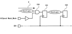
図1は、本実施形態に係る故障検出方法が適用される回路を示す回路図である。図1に示す回路は、遅延故障検出対象であるパスFと、遅延故障検出対象外であるタイミングフォルスパスEと、パスFの入力側に設けられるF/F101と、パスFの出力側に設けられるF/F102と、タイミングフォルスパスEの入力側に設けられるF/F103と、タイミングフォルスパスEとF/F101との間に設けられるマスク回路104と、マスク回路104を制御するマスク制御信号生成部200を有する。マスク制御信号生成部200はF/F201及びゲート202を有し、F/F201の出力がゲート202に入力される。
FIG. 1 is a circuit diagram showing a circuit to which the failure detection method according to this embodiment is applied. The circuit shown in FIG. 1 is provided on a path F that is a delay fault detection target, a timing false path E that is not a delay fault detection target, an F /
F/F101、102、103及びF/F201はCK1信号のクロックで動作する。F/F101、102、103の入力はScan In信号が入力されるスキャンパスDと、UserLogic In信号が入力されるユーザパス(タイミングフォルスパスE、パスF等)とが切り換えられる。当該切換動作はスキャンテストにおけるキャプチャー期間とシフト期間とを区別するScan Enable信号により制御される。言い換えると、Scan Enable信号とはキャプチャー信号である。また、Scan Enable信号はF/F201にも入力される。ゲート202はF/F201の出力(Scan Enable信号)の反転信号と、回路がテスト中であることを示すTest Mode信号との論理積を出力する。ゲート202の出力が、マスク回路104を制御するAtSpeed Mask_Mode信号として用いられる。マスク回路104はAtSpeed Mask_Mode信号の反転信号により制御される。
The F /
図1においては、タイミングフォルスパスE、パスFがユーザパスであり、UserLogic In信号が入力され、F/F101、102、103に入力されるCK1信号に基づいて動作する。スキャンパスDは当該回路のテストをする際に、各F/Fにラッチする信号を順次シフトさせながら入力するためのパスである。ユーザパスとスキャンパスDとは、Scan Enable信号によって選択される。即ち、Scan Enable信号が"1"の時はスキャンパスDが選択され、Scan Enable信号が"0"の時はユーザパスが選択される。
In FIG. 1, the timing false path E and path F are user paths, the UserLogic In signal is input, and the operation is performed based on the CK1 signal input to the F /
マスク回路104は、タイミングフォルスパスEを遅延故障検出対象外とするためのマスク回路であり、通常動作時にはTest Mode信号が"0"であるため、AtSpeed Mask_Mode信号は常に"0"となり、マスク回路104はタイミングフォルスパスEの信号をそのまま出力するため、通常動作時にはマスク回路104は回路に対して何ら影響を及ぼさない。テスト動作時には、Test Mode信号が"1"となり、Scan Enable信号及びCK1信号に基づいてAtSpeed Mask_Mode信号が決定される。AtSpeed Mask_Mode信号が"1"の時、マスク回路104の出力は常に"0"となり、タイミングフォルスパスEがマスクされることとなる。
The
マスク制御信号生成部200は図2に示すようにLogicBISTコントローラとスキャン対象回路との間に設けられる。LogicBISTコントローラで生成されるScan Enable信号とLogicBIST_Mode信号とに基づいてAtSpeed Mask_Mode信号が生成され、スキャン対象回路、本実施形態においてはマスク回路104に入力される。尚、図1においては、LogicBIST_Mode信号はTest Mode信号と示されている。
The mask control
図3はLSIの出荷テストの流れを示すフローチャートである。従来、テストパタンの作成(S404)はBIST回路を挿入(S401)し、Falseパスを指定してマスク回路を挿入(S402)した後に行っていた。本実施形態においては、Falseパスを指定した後にマスク制御信号生成部200を挿入(S403)してから、テストパタンの作成(S404)を行う。その後、出荷テストを行う(S405)。
FIG. 3 is a flowchart showing the flow of the LSI shipment test. Conventionally, a test pattern is created (S404) after inserting a BIST circuit (S401), specifying a False path, and inserting a mask circuit (S402). In the present embodiment, after specifying the False path, the mask control
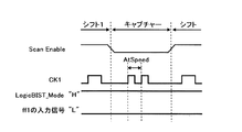
図4は図1に示す回路の動作を示すタイミングチャートである。図4(a)、(b)に示すシフト1期間においては、Scan Enable信号が"1"であり、F/F101、102、103の入力はスキャンパスDが選択されている。当該スキャンパスDを用いて各F/FにScan In信号を入力し、初期値を設定する。この時、Scan Enable信号を"1"としてCK1のクロックに従ってシフト動作を行なうため、F/F201の出力も"1"となり、AtSpeed Mask_Mode信号は"0"となる。
FIG. 4 is a timing chart showing the operation of the circuit shown in FIG. In the
図4にはシフト1期間の最終クロックのみ示されている。シフト1期間におけるシフト動作の最終クロックの時点では、F/F201の出力は"1"であり、AtSpeed Mask_Mode信号は"0"である。図4(a)を用いて動作の一例を説明する。図4(a)に示す例においては、F/F101の初期値として"0"を入力する。また、F/F103にはタイミングフォルスパスEからマスク回路104に入力される信号が"1"となるような初期値を入力する。
FIG. 4 shows only the final clock in the
シフト動作により各F/Fに初期値を入力後、Scan Enable信号を"0"としてキャプチャー期間に入る。キャプチャー期間においては、当該回路の実動作周波数(ユーザクロック)又はそれと同様の周波数でCK1信号が入力される。Scan Enable信号が"0"となったことにより、各F/Fの入力はスキャンパスDからユーザパスに切り換えられる。これにより、F/F201の入力は"0"となる。また、マスク回路104の出力、即ちF/F101の入力は"1"である。この状態において、キャプチャー期間の第1クロックにより、F/F101の出力は"0"から"1"に遷移する。また、F/F201の出力が"0"となり、AtSpeed Mask_Mode信号が"1"となるため、マスク回路104の出力は"0"に固定され、以後、タイミングフォルスパスEがマスクされることとなる。この状態での第2クロックにより、F/F101の出力が"1"から"0"に遷移する。また、第2クロックにおいては、タイミングフォルスパスEはマスクされており遅延故障検出対象外となるため、テスト精度に問題は生じない。
After the initial value is input to each F / F by the shift operation, the Scan Enable signal is set to “0” and the capture period starts. In the capture period, the CK1 signal is input at the actual operating frequency (user clock) of the circuit or a frequency similar thereto. When the Scan Enable signal becomes “0”, the input of each F / F is switched from the scan path D to the user path. As a result, the input of the F /
図4(b)を用いて、より一般的な場合について説明する。シフト1期間においては、Scan Enable信号が"1"であり、スキャンパスDを用いてF/F101、102、103に任意の初期値を入力する。図に示す通り、シフト1期間の最終クロックの状態においては、F/F101の入力はタイミングフォルスパスEの出力信号であり、F/F101の出力はシフト動作により入力された初期値である。この状態においてScan Enable信号を"0"としてキャプチャー期間に入る。キャプチャー期間の第1クロックにより、F/F101の出力はシフト動作によって入力された初期値から、F/F101に入力されていた値、即ちシフト1期間の最終クロック時点でのタイミングフォルスパスEの出力信号に遷移する。
A more general case will be described with reference to FIG. In the
また、F/F201の出力が"0"となり、AtSpeed Mask_Mode信号が"1"となるため、マスク回路104の出力、即ちF/F101の入力は"0"に固定され、以後、タイミングフォルスパスEがマスクされることとなる。この状態での第2クロックにより、F/F101の出力が"0"となる。この様に、マスク回路104を制御するAtSpeed Mask_Mode信号の生成においてScan Enable信号を用いることにより、キャプチャー期間の第1クロックまではタイミングフォルスパスEがマスクされず、当該第一クロックにおいてタイミングフォルスパスEを利用してF/F101の入力信号を遷移させることができる。
Further, since the output of the F /
従来技術においては、マスク回路を制御する信号は本実施形態に係るTest Mode信号のようにテスト中は不変であり、タイミングフォルスパスは常にマスクされた状態であったため、タイミングフォルスパスを利用して信号を遷移させることは不可能であった。しかしながら、本実施形態に係るマスク制御信号生成部200を用いることにより、キャプチャー期間の第1クロックのみ、タイミングフォルスパスEを用いて、その終点であるF/F101の入力信号を遷移させることが可能となる。従って、F/F101の初期値に"0"を選択し、第1クロックにおいてF/F101の値が"0"から"1"に遷移するようにF/F103の初期値を選択することにより、F/F101においてfall("1"から"0"への遷移)とrise("0"から"1"への遷移)との両方を検出することができ、パスFにおける遅延故障検出効果を100%とすることができる。
In the prior art, the signal for controlling the mask circuit is not changed during the test like the Test Mode signal according to this embodiment, and the timing false path is always masked. It was impossible to transition signals. However, by using the mask control
従来技術においては、タイミングフォルスパス以降のパスの遅延故障検出効果を100%とするために、通常スキャンパタンでの補完が必要であったが、本実施形態に係る故障検出方法及びマスク制御信号生成部200を用いることにより、その様な補完が不要となる。従って、スキャンパタン長の低減、スキャンパタン作成工数の削減を図ることができる。また、外部クロックを用いてテストを行う必要がなくなり、LSIの内部全体のパスを実動作周波数でテストすることが可能となる。
In the prior art, in order to set the delay fault detection effect of the path after the timing false path to 100%, it is necessary to supplement the normal scan pattern. However, the fault detection method and mask control signal generation according to the present embodiment By using the
本実施形態におけるマスク制御信号生成部200は、Scan Enable信号、Test Mode信号及びクロック信号であるCK1信号に基づき動作する。Scan Enable信号はスキャン手法を用いたテストを行なう場合は必ず必要となる信号である。また、Test Mode信号はテスト時に"1"、通常動作時に"0"となる信号であり、従来技術におけるLogicBIST_Mode信号と同様であっても構わない。従って、本実施形態に係るマスク制御信号生成部200を用いるだけで、容易に本実施形態に係る故障検出方法を実施することができる。
The mask control
以上説明したように、本発明の実施の形態1によれば、スキャン手法を用いたLSIの故障検出テストにおいて、スキャンパタン長の低減及び実動作周波数のみでのテストが可能となる。
実施の形態2.
As described above, according to the first embodiment of the present invention, it is possible to reduce the scan pattern length and test only at the actual operating frequency in the LSI failure detection test using the scanning method.
Embodiment 2. FIG.
実施の形態1においては、マスク回路104を制御することにより、キャプチャー時に一時的にタイミングフォルスパスEの信号を利用可能とすることで課題を解決した。本実施形態においては、従来技術と同様にタイミングフォルスパスEはマスクしたまま、他の方法によりタイミングフォルスパスの終点以降の入力信号を遷移させる方法を説明する。尚、実施の形態1と同様の符号を付す構成については実施の形態1と同一又は相当部を示し、説明を省略する。
In the first embodiment, the problem is solved by controlling the
図5は、本実施形態に係る故障検出方法が適用される回路を示す回路図である。図に示すように、本実施形態においては、マスク回路104はLogicBIST_Mode信号により直接制御される。即ち、当該回路のテスト中においては、マスク回路104の出力は常に"0"に固定されている。
FIG. 5 is a circuit diagram showing a circuit to which the failure detection method according to this embodiment is applied. As shown in the figure, in the present embodiment, the
マスク回路104とF/F101との間に代替信号生成部300を設ける。代替信号生成部300はF/F301及びゲート302を有し、F/F301の出力及びマスク回路104の出力がゲート302に入力される。ゲート302はマスク回路104の出力とF/F301の出力との排他的論理和を出力するEXOR回路である。
An alternative
F/F301はCK1とは異なるクロック信号CK2に基づいて動作する。F/F301には自身の出力信号及びScan In信号が入力され、いずれか一方がScan Enable信号により選択される。また、F/F301には出力信号を初期化するReset信号が入力される。
The F /
図に示されるように、本実施形態に係るF/F101の入力はScan Enable信号に関わらず代替信号生成部300の出力のみである。代替信号生成部300に含まれるF/F301はF/F101及びF/F102と共にシフトチェーンを構成しており、シフト値であるScan In信号はF/F301に入力され、CK2信号によって順次シフトされる。
As shown in the figure, the input of the F /
通常動作時はScan Enable信号及びLogicBIST_Mode信号が"0"である。従って、マスク回路104はタイミングフォルスパスEの信号をそのまま出力する。また、F/F301はCK2信号に従って自己の信号を繰り返し出力するが、通常動作に入るに際して、F/F301の値はReset信号により"0"になるので、F/F301の出力は通常動作時には"0"に固定される。従って、通常動作時の代替信号生成部300の出力、即ちF/F101の入力はタイミングフォルスパスEの出力と同様の信号である。
During normal operation, the Scan Enable signal and the LogicBIST_Mode signal are “0”. Therefore, the
テスト動作時は、LogicBIST_Mode信号が"1"である。従って、マスク回路104の出力は"0"に固定されるため、代替信号生成部300の出力、即ちF/F101の入力はF/F301の出力と同様の信号である。シフト動作時においては、Scan Enable信号が"1"となり、CK2信号に従ってScan In信号が順次入力される。キャプチャー時においては、Scan Enable信号が"0"となり、F/F301の出力はシフト動作時の最終クロックの値に固定される。即ち、本実施形態においては、タイミングフォルスパスEをマスク回路104によってマスクしながらも、タイミングフォルスパスEの終点にあたるF/F101の入力が"0"に固定されず、F/F301の値を用いてF/F101の値を遷移させることができる。
During the test operation, the LogicBIST_Mode signal is “1”. Therefore, since the output of the
図6は図5に示す回路の動作を示すタイミングチャートである。図6を用いて図5に示す回路の動作を説明する。シフト1期間においては、Scan Enable信号が"1"であり、CK1信号とCK2信号とを同期させ、Scan In信号を用いてF/F101、102及びF/F301に任意の初期値を入力する。図に示す通り、シフト1期間の最終クロックの状態においては、F/F101の入力はF/F301の出力信号であり、F/F101の出力はシフト動作により入力された初期値である。この状態においてScan Enable信号を"0"としてキャプチャー期間に入る。キャプチャー期間のCK1信号の第1クロックにより、F/F101の出力はシフト動作によって入力された初期値から、F/F101に入力されていた値、即ちシフト1期間の最終クロック時点でのF/F301の出力信号に遷移する。
FIG. 6 is a timing chart showing the operation of the circuit shown in FIG. The operation of the circuit shown in FIG. 5 will be described with reference to FIG. In the
ここで、キャプチャー期間においては、CK1信号とCK2信号とは同期しないため、CK1信号のAtSpeedテスト時においては、F/F101の入力信号はシフト1期間の最終クロック時点でのF/F301の出力信号に固定されている。従って、CK1信号の第2クロックにおいても、F/F101の出力は第1クロックと同様である。
Here, in the capture period, the CK1 signal and the CK2 signal are not synchronized. Therefore, during the AtSpeed test of the CK1 signal, the input signal of the F /
CK1信号とは別のタイミングに、CK2信号が動作する。Scan Enable信号は"0"であるため、F/F301は自己の出力信号を繰り返し出力する。キャプチャー期間において、CK1信号とCK2信号とは別のタイミングで動作するため、F/F301からF/F101にAtSpeed対象となるタイミングパスは発生しない。CK2を動作させるのは、主にCK2によって動作する他の回路のテストのためである。
The CK2 signal operates at a timing different from that of the CK1 signal. Since the Scan Enable signal is “0”, the F /
この様に、マスク回路104とF/F101との間に代替信号生成部300を設けることによって、キャプチャー期間におけるF/F101の入力信号が"0"に固定されず、F/F101の値を遷移させることができる。但しキャプチャー期間のCK1信号のAtSpeedテストにおいては、F/F301の出力信号は変化しないため、rise及びfallの両方を検出する場合は、キャプチャー動作を2回行なう必要がある。
As described above, by providing the substitute
以上説明したように、本発明の実施の形態2によれば、タイミングフォルスパスをマスクした状態において、タイミングフォルスパスの後段に入力される信号が"0"に固定されることなく遷移させることができる。 As described above, according to the second embodiment of the present invention, in a state where the timing false path is masked, the signal input to the subsequent stage of the timing false path can be shifted without being fixed to “0”. it can.
尚、上記の説明においては、F/F301はF/F101及びF/F102と共にシフトチェーンを構成していたが、これに限定されない。F/F301とF/F101及びF/F102とは異なるシフトチェーンに属し、夫々異なるScan In信号が入力されても良い。この場合においては、F/F101の入力は代替信号生成部300の出力と、Scan In信号とがScan Enable信号により選択されるように構成される。
その他の実施の形態.
In the above description, the F /
Other embodiments.
実施の形態1においては、回路内にマスク制御信号生成部200を設け、内部クロックに基づいてマスク回路104を制御したが、図7に示すように、AtSpeed Mask_Mode信号を外部から入力し、マスク回路104を直接制御することによっても、課題を解決することができる。即ち、実施の形態1のように、AtSpeed Mask_Mode信号をCK1信号及びScan Enable信号に基づいて生成し、制御するのはなく、外部機器でAtSpeed Mask_Mode信号を生成し、外部機器から直接マスク回路104を制御する。図2に示すタイミングと同様のタイミングでAtSpeed Mask_Mode信号を制御することにより、実施の形態1と同様の効果を得ることができる。
In the first embodiment, the mask control
この様な構成を用いることによって、マスク制御信号生成部200を設ける必要がなくなり、回路のオーバーヘッドを低減することができる。また、CK1信号、Scan Enable信号に関わらず、所望のタイミングでAtSpeed Mask_Mode信号を制御することができる。
By using such a configuration, it is not necessary to provide the mask control
1、3、4、5、6、7 F/F、2、8 マスク回路、9、10 ゲート
101、102、103 F/F、104 マスク回路、
200 マスク制御信号生成部、201 F/F、202 ゲート、
300 代替信号生成部、301 F/F、302 ゲート、
A、B、C パス、D スキャンパス、E タイミングフォルスパス、F パス、
1, 3, 4, 5, 6, 7 F / F, 2, 8 mask circuit, 9, 10
200 mask control signal generator, 201 F / F, 202 gate,
300 Substitute signal generator, 301 F / F, 302 gate,
A, B, C path, D scan campus, E timing false path, F path,
Claims (2)
前記ユーザ回路に含まれる故障検出対象外パスの後段に設けられ、当該故障検出対象外パスをマスクするためのマスク回路と、
前記故障検出対象外パス及び前記マスク回路の後段に位置する後続素子と、
前記テストにおいてキャプチャー期間であることを示すキャプチャー信号が入力され、前記テストのキャプチャー期間において前記スキャンパスに入力されるクロック信号に応じて前記キャプチャー信号を記憶し、同時に当該記憶した信号を出力する第1の制御素子と、
前記第1の制御素子の出力信号の反転信号と、前記ユーザ回路がテストモードであることを示すテストモード信号との論理積信号を前記マスク制御信号として出力する第2の制御素子と、を有し、
前記マスク回路は、前記故障検出対象外パスの信号と、当該マスク回路を制御するマスク制御信号の反転信号との論理積信号を出力し、
前記後続素子は、前記論理積信号により設定された論理値に基づき前記第1クロックに応じて立ち上がり若しくは立下りの任意の信号を出力するテスト回路。 A test circuit for testing a user circuit by a scan path,
A mask circuit for masking the non-failure detection target path, provided at a subsequent stage of the non-failure detection target path included in the user circuit;
The failure detection target path and the succeeding element located in the subsequent stage of the mask circuit;
A capture signal indicating a capture period in the test is input, the capture signal is stored in accordance with a clock signal input to the scan path in the capture period of the test, and the stored signal is output simultaneously. 1 control element;
A second control element that outputs a logical product signal of the inverted signal of the output signal of the first control element and a test mode signal indicating that the user circuit is in a test mode as the mask control signal; And
The mask circuit outputs a logical product signal of the signal of the failure detection target path and an inverted signal of a mask control signal for controlling the mask circuit;
The succeeding element is a test circuit that outputs an arbitrary signal rising or falling according to the first clock based on a logical value set by the logical product signal .
前記テストにおいてキャプチャー期間であることを示すキャプチャー信号が入力され、前記テストのキャプチャー期間において前記スキャンパスに入力されるクロック信号に応じて前記キャプチャー信号を記憶し、同時に当該記憶した信号を出力する第1の制御素子と、
前記第1の制御素子の出力信号の反転信号と、前記ユーザ回路がテストモードであることを示すテストモード信号との論理積信号を前記マスク回路を制御する制御信号として出力する第2の制御素子と、を有し、
前記クロック信号のうち、少なくとも第1クロックの立ち上がりに応じて前記故障検出対象外パスをマスクするように前記マスク回路を制御するマスク制御回路。 A mask control circuit for controlling a mask circuit for masking a path not included in the failure detection included in the user circuit when the user circuit is tested by a scan path,
A capture signal indicating a capture period in the test is input, the capture signal is stored in accordance with a clock signal input to the scan path in the capture period of the test, and the stored signal is output simultaneously. 1 control element;
A second control element that outputs a logical product signal of an inverted signal of the output signal of the first control element and a test mode signal indicating that the user circuit is in a test mode as a control signal for controlling the mask circuit And having
Before Among chrysanthemum lock signal, the mask control circuit for controlling the mask circuit to mask the fault detection object out path in response to a rising edge of the at least first clock.
Priority Applications (1)
| Application Number | Priority Date | Filing Date | Title |
|---|---|---|---|
| JP2005127862A JP4806537B2 (en) | 2005-04-26 | 2005-04-26 | Test circuit and mask control circuit |
Applications Claiming Priority (1)
| Application Number | Priority Date | Filing Date | Title |
|---|---|---|---|
| JP2005127862A JP4806537B2 (en) | 2005-04-26 | 2005-04-26 | Test circuit and mask control circuit |
Publications (3)
| Publication Number | Publication Date |
|---|---|
| JP2006308302A JP2006308302A (en) | 2006-11-09 |
| JP2006308302A5 JP2006308302A5 (en) | 2010-09-02 |
| JP4806537B2 true JP4806537B2 (en) | 2011-11-02 |
Family
ID=37475375
Family Applications (1)
| Application Number | Title | Priority Date | Filing Date |
|---|---|---|---|
| JP2005127862A Expired - Fee Related JP4806537B2 (en) | 2005-04-26 | 2005-04-26 | Test circuit and mask control circuit |
Country Status (1)
| Country | Link |
|---|---|
| JP (1) | JP4806537B2 (en) |
Families Citing this family (2)
| Publication number | Priority date | Publication date | Assignee | Title |
|---|---|---|---|---|
| US8441277B2 (en) | 2007-12-28 | 2013-05-14 | Nec Corporation | Semiconductor testing device, semiconductor device, and testing method |
| WO2010073399A1 (en) * | 2008-12-26 | 2010-07-01 | 株式会社ルネサステクノロジ | Semiconductor integrated circuit design method and software |
Family Cites Families (6)
| Publication number | Priority date | Publication date | Assignee | Title |
|---|---|---|---|---|
| JPH11133120A (en) * | 1997-10-31 | 1999-05-21 | Mitsubishi Electric Corp | Semiconductor device test pattern generating method, and computer-readable recording medium recording semiconductor device test pattern generating program |
| JP2001249164A (en) * | 2000-03-03 | 2001-09-14 | Hitachi Ltd | Lis with built-in type self-test circuit |
| JP2002148309A (en) * | 2000-11-13 | 2002-05-22 | Hitachi Ltd | Semiconductor integrated circuit |
| JP2003344493A (en) * | 2002-05-24 | 2003-12-03 | Mitsubishi Electric Corp | Semiconductor device evaluator |
| JP2004170244A (en) * | 2002-11-20 | 2004-06-17 | Matsushita Electric Ind Co Ltd | Built-in self-checking circuit |
| JP2005017067A (en) * | 2003-06-25 | 2005-01-20 | Matsushita Electric Ind Co Ltd | Semiconductor integrated circuit incorporating self-testing circuit, and method for diagnosing fault in the semiconductor integrated circuit |
-
2005
- 2005-04-26 JP JP2005127862A patent/JP4806537B2/en not_active Expired - Fee Related
Also Published As
| Publication number | Publication date |
|---|---|
| JP2006308302A (en) | 2006-11-09 |
Similar Documents
| Publication | Publication Date | Title |
|---|---|---|
| JP5256840B2 (en) | Logic circuit | |
| JP4815326B2 (en) | Integrated circuit timing failure improvement apparatus, integrated circuit timing failure diagnosis apparatus and method, and integrated circuit | |
| JP6054597B2 (en) | Semiconductor integrated circuit | |
| JP2008275479A (en) | Scan test circuit, scan test control method | |
| US11120187B1 (en) | Semiconductor integrated circuit, circuit designing apparatus, and circuit designing method | |
| JP5032395B2 (en) | Test condition generation method and test condition generation apparatus | |
| JPWO2006132329A1 (en) | Microcomputer and its test method | |
| US7778790B2 (en) | Semiconductor integrated circuit device and delay fault testing method | |
| JP2006329737A (en) | Semiconductor integrated circuit device and its test method | |
| JP2004184316A (en) | Scanning test circuit | |
| US6799292B2 (en) | Method for generating test pattern for semiconductor integrated circuit and method for testing semiconductor integrated circuit | |
| JP4806537B2 (en) | Test circuit and mask control circuit | |
| JP2006292646A (en) | Method for testing lsi | |
| JP7169044B2 (en) | Semiconductor integrated circuit, its design method, program and storage medium | |
| JP5179861B2 (en) | Semiconductor device | |
| US6976199B2 (en) | AC LSSD/LBIST test coverage enhancement | |
| JP2005257366A (en) | Semiconductor circuit device and scan test method concerning semiconductor circuit | |
| JP2006194727A (en) | Method for testing integrated circuit | |
| JP2008064717A (en) | Delay measuring circuit in semiconductor integrated circuit | |
| US8539327B2 (en) | Semiconductor integrated circuit for testing logic circuit | |
| JP2013088400A (en) | Method for inspecting semiconductor integrated circuit, and the semiconductor integrated circuit | |
| JP4650928B2 (en) | Scan flip-flop circuit, scan test circuit and test design method using the same | |
| JP5426933B2 (en) | Failure detection method for semiconductor integrated device | |
| JP3573692B2 (en) | Scan path circuit, scan path circuit generation method, and recording medium recording the program | |
| JP5499528B2 (en) | Semiconductor integrated circuit and electronic equipment |
Legal Events
| Date | Code | Title | Description |
|---|---|---|---|
| A621 | Written request for application examination |
Free format text: JAPANESE INTERMEDIATE CODE: A621 Effective date: 20080314 |
|
| A977 | Report on retrieval |
Free format text: JAPANESE INTERMEDIATE CODE: A971007 Effective date: 20100617 |
|
| A521 | Request for written amendment filed |
Free format text: JAPANESE INTERMEDIATE CODE: A523 Effective date: 20100714 |
|
| A131 | Notification of reasons for refusal |
Free format text: JAPANESE INTERMEDIATE CODE: A131 Effective date: 20101019 |
|
| A521 | Request for written amendment filed |
Free format text: JAPANESE INTERMEDIATE CODE: A523 Effective date: 20101208 |
|
| TRDD | Decision of grant or rejection written | ||
| A01 | Written decision to grant a patent or to grant a registration (utility model) |
Free format text: JAPANESE INTERMEDIATE CODE: A01 Effective date: 20110809 |
|
| A01 | Written decision to grant a patent or to grant a registration (utility model) |
Free format text: JAPANESE INTERMEDIATE CODE: A01 |
|
| A61 | First payment of annual fees (during grant procedure) |
Free format text: JAPANESE INTERMEDIATE CODE: A61 Effective date: 20110815 |
|
| R150 | Certificate of patent or registration of utility model |
Free format text: JAPANESE INTERMEDIATE CODE: R150 |
|
| FPAY | Renewal fee payment (event date is renewal date of database) |
Free format text: PAYMENT UNTIL: 20140819 Year of fee payment: 3 |
|
| S531 | Written request for registration of change of domicile |
Free format text: JAPANESE INTERMEDIATE CODE: R313531 |
|
| R350 | Written notification of registration of transfer |
Free format text: JAPANESE INTERMEDIATE CODE: R350 |
|
| LAPS | Cancellation because of no payment of annual fees |