JP4804082B2 - Image forming apparatus - Google Patents
Image forming apparatus Download PDFInfo
- Publication number
- JP4804082B2 JP4804082B2 JP2005267694A JP2005267694A JP4804082B2 JP 4804082 B2 JP4804082 B2 JP 4804082B2 JP 2005267694 A JP2005267694 A JP 2005267694A JP 2005267694 A JP2005267694 A JP 2005267694A JP 4804082 B2 JP4804082 B2 JP 4804082B2
- Authority
- JP
- Japan
- Prior art keywords
- beams
- image forming
- image
- toner
- forming apparatus
- Prior art date
- Legal status (The legal status is an assumption and is not a legal conclusion. Google has not performed a legal analysis and makes no representation as to the accuracy of the status listed.)
- Expired - Fee Related
Links
Images


Classifications
-
- B—PERFORMING OPERATIONS; TRANSPORTING
- B41—PRINTING; LINING MACHINES; TYPEWRITERS; STAMPS
- B41J—TYPEWRITERS; SELECTIVE PRINTING MECHANISMS, i.e. MECHANISMS PRINTING OTHERWISE THAN FROM A FORME; CORRECTION OF TYPOGRAPHICAL ERRORS
- B41J29/00—Details of, or accessories for, typewriters or selective printing mechanisms not otherwise provided for
- B41J29/38—Drives, motors, controls or automatic cut-off devices for the entire printing mechanism
- B41J29/393—Devices for controlling or analysing the entire machine ; Controlling or analysing mechanical parameters involving printing of test patterns
-
- G—PHYSICS
- G03—PHOTOGRAPHY; CINEMATOGRAPHY; ANALOGOUS TECHNIQUES USING WAVES OTHER THAN OPTICAL WAVES; ELECTROGRAPHY; HOLOGRAPHY
- G03G—ELECTROGRAPHY; ELECTROPHOTOGRAPHY; MAGNETOGRAPHY
- G03G15/00—Apparatus for electrographic processes using a charge pattern
- G03G15/04—Apparatus for electrographic processes using a charge pattern for exposing, i.e. imagewise exposure by optically projecting the original image on a photoconductive recording material
- G03G15/043—Apparatus for electrographic processes using a charge pattern for exposing, i.e. imagewise exposure by optically projecting the original image on a photoconductive recording material with means for controlling illumination or exposure
- G03G15/0435—Apparatus for electrographic processes using a charge pattern for exposing, i.e. imagewise exposure by optically projecting the original image on a photoconductive recording material with means for controlling illumination or exposure by introducing an optical element in the optical path, e.g. a filter
Landscapes
- Physics & Mathematics (AREA)
- General Physics & Mathematics (AREA)
- Facsimile Scanning Arrangements (AREA)
- Control Or Security For Electrophotography (AREA)
- Laser Beam Printer (AREA)
- Fax Reproducing Arrangements (AREA)
Description
本発明は、電子写真技術を用いて画像を形成するデジタル複写機、ファクシミリ、レーザープリンター、これらの機能を複合的に併せ持つデジタル複写機等に関する。特に、複数のビームにより複数のラインを走査して画像を形成するマルチビームを用いる画像形成装置に関する。
The present invention relates to a digital copying machine, a facsimile machine, a laser printer, and a digital copying machine having a combination of these functions for forming an image using electrophotographic technology. In particular, it relates to an image forming equipment using the multi-beam to form an image by scanning a plurality of lines by a plurality of beams.
従来より、像担持体としてのドラム状の電子写真感光体、即ち感光体ドラム上にレーザビーム光などの発光素子による光を照射するレーザ光走査光学系を用いて、電子写真プロセスによって感光体ドラム上に静電潜像を形成する画像形成装置が知られている。 Conventionally, a drum-shaped electrophotographic photosensitive member as an image carrier, that is, a photosensitive drum by an electrophotographic process using a laser beam scanning optical system that irradiates light on a photosensitive drum with a light emitting element such as a laser beam. An image forming apparatus that forms an electrostatic latent image thereon is known.
近年、この画像形成装置に対して、画像形成の高速化と画像形成密度(解像度)の向上が求められている。この要求に対応するために、主走査方向は各画素を形成するための画像クロックを高速化し、副走査方向はポリゴンモータの回転速度を高速化することで実現している。 In recent years, this image forming apparatus is required to increase the speed of image formation and improve the image formation density (resolution). In order to meet this requirement, the main scanning direction is realized by increasing the image clock for forming each pixel, and the sub-scanning direction is realized by increasing the rotation speed of the polygon motor.
しかしながら、ポリゴンモータは回転速度の高速化に限界があるため、更なる高速化の方法として1回の走査で同時にかつ平行に複数のレーザ光を感光体上に走査するマルチビーム走査光学系が提案されている。このマルチビーム走査光学系では、レーザ光による走査速度は1/(レーザ素子数)に制御されて感光体ドラム上に画像が形成されている。 However, since there is a limit to the speedup of the rotation speed of the polygon motor, a multibeam scanning optical system that scans a plurality of laser beams simultaneously and in parallel in one scan is proposed as a method for further speedup. Has been. In this multi-beam scanning optical system, the scanning speed by laser light is controlled to 1 / (number of laser elements), and an image is formed on the photosensitive drum.
マルチビーム光学系を用いて各レーザ光を感光体上に走査する構成では、各光学素子の光学特性の製法時にばらつきを生じると主走査方向の走査倍率が一致しなくなり画質が低下するので、この不一致を補正して等倍性となるような処理が必要である。 In a configuration in which each laser beam is scanned on the photosensitive member using a multi-beam optical system, if the optical characteristics of each optical element vary during the manufacturing process, the scanning magnification in the main scanning direction will not match and the image quality will deteriorate. Processing that corrects the inconsistency and makes it equal in size is necessary.
この問題を解決するためには、主走査方向の走査倍率を決定するパラメータの1つであるレーザ変調速度を各々のレーザで別々に調整可能とし、各ビームの感光体上の走査倍率を一定かつ等倍に走査可能にして、より高画質の画像を形成可能にしなければならない。そこで、主走査方向の先端と後端部にBDセンサを配置し、各ビームの主走査倍率をBDセンサで検知し、各ビームの画像クロック周波数を微調することで主走査倍率を補正する方法が提案されている(特許文献1参照)。
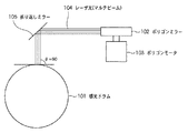
ここで、従来のマルチビーム走査光学系を用いる画像形成装置におけるレーザ光の走査入射角の違いによる画質低下の問題について、図1〜4を用いて説明する。図1は、周知のレーザ走査ユニットである。不図示のレーザダイオードから照射されたレーザ光(図は4ビームの例)104は、ポリゴンモータ103によって所定の回転数で回転駆動するポリゴンミラー102および折り返しミラー105を介して、感光ドラム101上を走査するように制御されている。
Here, the problem of image quality degradation due to the difference in the scanning incident angle of laser light in an image forming apparatus using a conventional multi-beam scanning optical system will be described with reference to FIGS. FIG. 1 shows a known laser scanning unit. Laser light (illustrated as an example of four beams) 104 emitted from a laser diode (not shown) passes on the photosensitive drum 101 via a
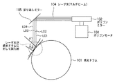
図2は、図1の一部を上部から見た図であり、ポリゴンミラーが図の矢印方向に回転駆動することによりレーザ光は図のように走査され、レーザ光の光路中にはBDセンサ106、107が配置される。BDセンサ106はレーザ走査方向の先端、BDセンサ107はレーザ走査方向の後端にそれぞれ配置され、主走査方向の同期信号出力と主走査倍率検知(走査長差の検知)を行なっている。
FIG. 2 is a view of a part of FIG. 1 as viewed from above, and the polygon mirror is driven to rotate in the direction of the arrow in the figure, so that the laser beam is scanned as shown in the figure. 106 and 107 are arranged. The
ここで、図1のように感光ドラム101へのレーザ光の走査入射角θが各ビームともほぼ同じであれば、レーザ光の走査入射角の違いによる画質の低下は起こらない。 Here, as shown in FIG. 1, if the scanning incident angle θ of the laser beam on the photosensitive drum 101 is substantially the same for each beam, the image quality is not deteriorated due to the difference in the scanning incident angle of the laser beam.
しかしながら、通常の画像形成装置では、図3に示すように、感光ドラムからの反射による戻り光を低減させるため、あるいは、画像形成装置の小型化するなどの制約から、レーザ光の走査入射角が図のθ1、θ2に示すように異なってしまう。このため、BDセンサ配置位置では正しい走査倍率であったものが、図3に示す感光ドラム上ではレーザ光の走査入射角の差により走査倍率が異なることになり、その結果として、図4に示すようにレーザビームの感光ドラム101上での走査長が異なってしまう。 However, in a normal image forming apparatus, as shown in FIG. 3, the scanning incident angle of the laser beam is reduced in order to reduce the return light due to reflection from the photosensitive drum or due to restrictions such as downsizing of the image forming apparatus. They are different as shown by θ1 and θ2 in the figure. For this reason, the correct scanning magnification at the position where the BD sensor is arranged is different on the photosensitive drum shown in FIG. 3 due to the difference in the scanning incident angle of the laser beam. As a result, as shown in FIG. Thus, the scanning length of the laser beam on the photosensitive drum 101 is different.
図4は、図3に示す4本のレーザ走査光LD1〜LD4によって感光体上に形成されたトナー像を示すものであり、図4に示すようなに走査長差、すなわち、走査方向の感光体ドラム上に形成されたトナー像の長さの差を生じる。このようにレーザビームの感光ドラム101上での走査長が異なると、縦線揺らぎ等が発生するため、画質低下を生じる場合があるという問題が発生する。 FIG. 4 shows a toner image formed on the photosensitive member by the four laser scanning lights LD1 to LD4 shown in FIG. 3, and as shown in FIG. 4, the difference in scanning length, that is, the photosensitive in the scanning direction. A difference in the length of the toner image formed on the body drum is generated. In this way, when the scanning length of the laser beam on the photosensitive drum 101 is different, vertical line fluctuations and the like occur, which causes a problem that image quality may be deteriorated.
本発明は、上記説明した従来技術の問題点を解決することを出発点としてなされたものである。その目的は、複数のビームにより複数のラインを走査して画像を形成する際に、感光体ドラム上へのレーザ光の走査入射角が各ビームによって異なる場合でもそれによる画質低下を低減する画像形成装置を提供することである。
The present invention has been made starting from solving the above-described problems of the prior art. The purpose is to form an image that reduces image quality degradation even when the scanning incident angle of the laser beam on the photosensitive drum varies depending on each beam when scanning multiple lines with multiple beams to form an image. it is to provide the equipment.
上記目的を達成するための本発明に係る画像形成装置は、以下の構成を有する。すなわち、感光体の回転方向において前記感光体上の異なる位置に複数のビームが照射されるよう配列された複数の光源を有し、前記複数のビームを、所定の回転速度で回転する前記感光体上の所定の方向に走査させることによって前記感光体上に静電潜像を形成し、前記静電潜像をトナー像に現像する画像形成手段を備える画像形成装置であって、前記感光体上を走査する前記複数のビームのうち前記回転方向の両端を走査するビームそれぞれにより前記感光体上に複数のトナーパターンが形成されるように前記画像形成手段を制御するパターン形成手段と、前記感光体の回転方向の両端を走査するビームそれぞれにより形成された前記複数のトナーパターンを検出する検出手段と、前記検出手段の検出結果に基づいて、前記複数のビームそれぞれによって形成される前記トナー像の前記所定の方向における長さが等しくなる様に前記複数の光源それぞれからのビームを出射させるタイミングを制御する光源制御手段と、前記画像形成手段が前記複数のトナーパターンを形成する際に前記感光体の回転速度を前記所定の回転速度よりも減速させる速度制御手段と、を備えており、前記トナー像は所定の解像度で形成され、前記感光体上を走査する隣り合うビームの間隔が前記所定の解像度に応じた間隔になるように前記複数の光源は配列され、前記複数のビームの数をNとした場合に、前記速度制御手段は、前記複数のトナーパターンが前記所定の解像度で形成されるように前記感光体の回転速度を1/Nに減速させることを特徴とする。また、画像形成装置は、感光体の回転方向において前記感光体上の異なる位置に複数のビームが照射されるよう配列された複数の光源を有し、前記複数のビームを、所定の回転速度で回転する前記感光体上の所定の方向に走査させることによって前記感光体上に静電潜像を形成し、前記静電潜像をトナー像に現像する画像形成手段を備える画像形成装置であって、前記感光体上を走査する前記複数のビームのうち前記回転方向の両端を走査するビームそれぞれにより前記感光体上に複数のトナーパターンが形成されるように前記画像形成手段を制御するパターン形成手段と、前記感光体の回転方向の両端を走査するビームそれぞれにより形成された前記複数のトナーパターンを検出する検出手段と、前記検出手段の検出結果に基づいて、前記複数のビームそれぞれによって形成される前記トナー像の前記所定の方向における長さが等しくなる様に、前記複数の光源それぞれからのビームを出射させるタイミングを制御する光源制御手段と、前記画像形成手段が前記複数のトナーパターンを形成する際に前記感光体の回転速度を前記所定の回転速度よりも減速させる速度制御手段と、を備えており、前記画像形成手段は、前記感光体の回転速度に同期するように回転駆動され、前記感光体上の前記トナー像が転写される中間転写体と、前記中間転写体上に転写されたトナー像を記録媒体に転写する転写手段と、を備えており、前記検出手段は、前記中間転写体上に転写された前記複数のトナーパターンを検出し、前記速度制御手段は、前記複数のトナーパターンを形成する際に前記中間転写体の回転速度を減速させ、前記トナー像は所定の解像度で形成され、前記感光体上を走査する隣り合うビームの間隔が前記所定の解像度に応じた間隔になるように前記複数の光源は配列され、前記複数のビームの数をNとした場合に、前記速度制御手段は、前記感光体上の前記複数のトナーパターンが前記所定の解像度で前記中間転写体に転写されるように前記中間転写体の回転速度を1/Nに減速させることを特徴とする。 In order to achieve the above object, an image forming apparatus according to the present invention has the following arrangement. That is, the photoconductor having a plurality of light sources arranged so that a plurality of beams are irradiated to different positions on the photoconductor in the rotation direction of the photoconductor, and rotating the plurality of beams at a predetermined rotation speed. An image forming apparatus comprising image forming means for forming an electrostatic latent image on the photosensitive member by scanning in a predetermined direction on the photosensitive member, and developing the electrostatic latent image into a toner image. A pattern forming unit that controls the image forming unit so that a plurality of toner patterns are formed on the photoconductor by each of the beams that scan both ends of the rotation direction among the plurality of beams that scan the image; and the photoconductor Detecting means for detecting the plurality of toner patterns formed by the respective beams that scan both ends in the rotation direction of the plurality of beams, and the plurality of beams based on the detection result of the detecting means Light source control means for controlling the timing of emitting the beam from each of the plurality of light sources so that the lengths of the toner images formed by each in the predetermined direction are equal, and the image forming means includes the plurality of image forming means. Speed control means for decelerating the rotational speed of the photoconductor from the predetermined rotational speed when forming the toner pattern, and the toner image is formed with a predetermined resolution, and is formed on the photoconductor. When the plurality of light sources are arranged so that an interval between adjacent beams to be scanned is an interval according to the predetermined resolution, and the number of the plurality of beams is N, the speed control means The rotational speed of the photosensitive member is reduced to 1 / N so that a toner pattern is formed at the predetermined resolution . Further, the image forming apparatus includes a plurality of light sources arranged so that a plurality of beams are irradiated to different positions on the photoconductor in the rotation direction of the photoconductor, and the plurality of beams are transmitted at a predetermined rotation speed. An image forming apparatus including an image forming unit configured to form an electrostatic latent image on the photosensitive member by scanning in a predetermined direction on the rotating photosensitive member, and to develop the electrostatic latent image into a toner image. A pattern forming unit that controls the image forming unit so that a plurality of toner patterns are formed on the photoconductor by each of the beams that scan both ends of the rotation direction among the plurality of beams that scan the photoconductor; And detecting means for detecting the plurality of toner patterns formed by the respective beams that scan both ends of the photosensitive member in the rotation direction, and based on the detection result of the detecting means, A light source control means for controlling the timing of emitting the beams from each of the plurality of light sources, and the image forming means so that the lengths of the toner images formed by each of the plurality of beams are equal in the predetermined direction. Speed control means for reducing the rotational speed of the photoreceptor below the predetermined rotational speed when forming the plurality of toner patterns, and the image forming means is synchronized with the rotational speed of the photoreceptor. And an intermediate transfer member to which the toner image on the photosensitive member is transferred, and transfer means for transferring the toner image transferred onto the intermediate transfer member to a recording medium. The detection means detects the plurality of toner patterns transferred onto the intermediate transfer member, and the speed control means detects the medium patterns when forming the plurality of toner patterns. The plurality of light sources are configured such that the rotational speed of the transfer body is reduced, the toner image is formed with a predetermined resolution, and the interval between adjacent beams that scan on the photoconductor is an interval according to the predetermined resolution. When the number of the plurality of beams arranged is N, the speed control unit is configured to transfer the plurality of toner patterns on the photoconductor to the intermediate transfer body at the predetermined resolution. The rotational speed of the transfer body is reduced to 1 / N.
本発明によれば、複数のビームにより複数のラインを走査して画像を形成する画像形成装置において、各ビーム間の走査長差を簡単な構成で補正することができる。そのため、感光体ドラム上へのレーザ光の走査入射角が各ビームによって異なる場合でも、それによる画質低下を低減する画像形成装置およびその制御方法を提供することができる。 According to the present invention, in an image forming apparatus that scans a plurality of lines with a plurality of beams to form an image, the scanning length difference between the beams can be corrected with a simple configuration. Therefore, even when the scanning incident angle of the laser beam on the photosensitive drum is different for each beam, it is possible to provide an image forming apparatus and a control method therefor that can reduce image quality degradation caused by the beam.
<本実施形態の特徴>
本実施形態の画像形成装置は、複数のビームを感光体ドラム上で走査する時の各ビーム間の走査長差を検出するパターンを、配列方向の両端のビームのみでそれぞれ形成する。そして、形成されたパターンの走査方向の先端および後端の位置を検出して両端のビームの走査長差ΔLを算出し、算出された走査長差に基づいて、各ビーム間の走査長差をそれぞれ補正する補正量を算出して、各ビームの走査長差を補正することができる。そのため本画像形成装置では、感光体ドラム上へのレーザ光の走査入射角が各ビームによって異なる場合でも、走査入射角の差異によって生じる各ビームの走査長差動を補正することにより画質低下を低減することができる。
<Features of this embodiment>
The image forming apparatus according to the present embodiment forms a pattern for detecting a scanning length difference between each beam when scanning a plurality of beams on a photosensitive drum, using only the beams at both ends in the arrangement direction. Then, the positions of the leading and trailing ends in the scanning direction of the formed pattern are detected to calculate the scanning length difference ΔL between the beams at both ends. Based on the calculated scanning length difference, the scanning length difference between the beams is calculated. A correction amount to be corrected can be calculated to correct the scanning length difference of each beam. Therefore, in this image forming apparatus, even when the scanning incident angle of the laser beam on the photosensitive drum is different for each beam, the image quality deterioration is reduced by correcting the scanning length differential of each beam caused by the difference in the scanning incident angle. can do.
<本実施形態の画像形成装置の構成例>
以下、図面を参照しながら、本発明に係る実施形態の画像形成装置の詳細について説明する。
<Example of Configuration of Image Forming Apparatus of Present Embodiment>
Hereinafter, an image forming apparatus according to an embodiment of the present invention will be described in detail with reference to the drawings.
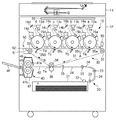
(画像形成装置の要部断面及びその動作例:図5)
図5は、本発明の第1の実施形態の画像形成装置の一例を示す要部断面図である。以下に説明する本実施形態の画像形成装置は、電子写真方式であり、本発明が特に有効であると考えられる複数の画像形成部10を並列に配しかつ中間転写方式を採用したカラー画像形成装置を一例として説明する。
(Cross section of the image forming apparatus and its operation example: FIG. 5)
FIG. 5 is a cross-sectional view of the main part showing an example of the image forming apparatus according to the first embodiment of the present invention. The image forming apparatus of the present embodiment described below is an electrophotographic system, and a color image forming system in which a plurality of
カラー画像形成装置は画像読取部1Rと画像出力部1Pからなる。画像読取部1Rは原稿画像を光学的に読み取り、電気信号に変換して画像出力部1Pに送るが、その詳細な説明は省略する。画像出力部1Pは大別して、画像形成部10(4つのステーションa、b、c、dが並設されており、その構成は同一である。)、給紙ユニット20、中間転写ユニット30、定着ユニット40、クリーニングユニット50、光センサユニット60および制御ユニット70から構成される。
The color image forming apparatus includes an
さらに、個々のユニットについて詳しく説明する。画像形成部10は次に述べるような構成になっている。像担持体としての感光ドラム11a、11b、11c、11dがその中心で軸支され、矢印方向に回転駆動される。感光ドラム11a〜11dの外周面に対向してその回転方向に一次帯電器12a、12b、12c、12d、光学系13a、13b、13c、13d、折り返しミラー16a、16b、16c、16d、現像部14a、14b、14c、14dが配置されている。一次帯電器12a〜12dにおいて感光ドラム11a〜11dの表面に均一な帯電量の電荷を与える。
Further, each unit will be described in detail. The
次いで光学系13a〜13dにより、記録画像信号に応じて変調した例えばレーザビームなどの光線を折り返しミラー16a〜16dを介して感光ドラム11a〜11d上に露光させることによって、そこに静電潜像を形成する。さらに、イエロー、シアン、マゼンタ、ブラックといった4色の現像剤(以下、これをトナーと呼ぶ)をそれぞれ収納した現像部14a〜14dによって上記静電潜像を顕像化する。顕像化された可視画像を中間転写体に転写する画像転写領域Ta、Tb、Tc、Tdの下流側では、クリーニング部15a、15b、15c、15dにより転写材に転写されずに感光ドラム11a〜11d上に残されたトナーを掻き落としてドラム表面の清掃を行う。以上に示したプロセスにより、各トナーによる画像形成が順次行われる。
Next, the
給紙ユニット20は、給紙ローラ対23、給紙ガイド24、およびレジストローラ25から成る。給紙ローラ対23及び給紙ガイド24は、記録材Pを収納するためのカセット21から記録材Pを一枚ずつ送り出すためのピックアップローラ22から送り出された記録材Pをレジストローラ25まで搬送する。レジストローラ25は、画像形成部10の画像形成タイミングに合わせて記録材Pを二次転写領域Teへ送り出す。
The
中間転写ユニット30について詳細に説明する。中間転写ベルト31は、中間転写ベルト31に駆動を伝達する駆動ローラ32、中間転写ベルト31の回動に従動する従動ローラ33、ベルトを挟んで二次転写領域Teに対向する二次転写対向ローラ34に巻回させる。これらのうち駆動ローラ32と従動ローラ33の間に一次転写平面Aが形成される。駆動ローラ32は金属ローラの表面に数mm厚のゴム(ウレタンまたはクロロプレン)をコーティングしてベルトとのスリップを防いでいる。駆動ローラ32はパルスモータ(不図示)によって回転駆動される。
The
各感光ドラム11a〜11dと中間転写ベルト31が対向する一次転写領域Ta〜Tdには、中間転写ベルト31の裏に一次転写用帯電器35a〜35dが配置されている。二次転写対向ローラ34に対向して二次転写ローラ36が配置され、中間転写ベルト31とのニップによって二次転写領域Teを形成する。二次転写ローラ36は中間転写体に対して適度な圧力で加圧されている。また、中間転写ベルト上、二次転写領域Teの下流には中間転写ベルト31の画像形成面をクリーニングするためのクリーニングユニット50(ブレード51、および廃トナーを収納する廃トナーボックス52)が設けられている。
定着ユニット40は、定着ローラ41a、加圧ローラ41b、ガイド43、定着断熱カバー46、47、内排紙ローラ44、外排紙ローラ45、転写材Pを積載する排紙トレー48などから成る。定着ローラ41aは、内部にハロゲンヒーターなどの熱源を備えており、そのローラに加圧される加圧ローラ41bにも熱源を備える場合がある。ガイド43は、上記ローラ対のニップ部へ転写材Pを導くものであり、定着断熱カバー46、47は、定着ユニットの熱を内部で閉じ込めるためのものである。内排紙ローラ44、外排紙ローラ45、は。上記ローラ対から排出されてきた転写材Pをさらに装置外部に導き出すためのものである。
The fixing
レジスト(色ずれ)検知センサ60は、中間転写ベルト31上に形成されたレジストレーション補正用パターン画像や濃度補正用パターン画像を読み取る。その結果を基にレジストレーション(色ずれ)補正および濃度/階調補正を行い、画像品位の向上を図る。
The registration (color misregistration)
制御ユニット70は、上記各ユニット内の機構の動作を制御するためのCPU(不図示)、制御プログラムや各種データを格納したROM(不図示)、RAM(不図示)、モータドライバ部(不図示)などから成る。CPUは制御プログラムに基づいてRAM(不図示)を動作領域として使用しモータドライバ部(不図示)などの各部を制御しながら、後で詳しく説明する主走査倍率の補正などの各種処理を行う。
The
次に、画像形成装置の動作を説明する。 Next, the operation of the image forming apparatus will be described.
CPU(不図示)より画像形成動作開始信号が発せられると、まずピックアップローラ22により、カセット21から転写材Pが一枚ずつ送り出される。そして給紙ローラ対23によって転写材Pが給紙ガイド24の間を案内されてレジストローラ25まで搬送される。その時レジストローラは停止されており、紙先端はニップ部に突き当たる。その後、画像形成部10が画像の形成を開始するタイミングに合わせてレジストローラは回転を始める。この回転時期は、転写材Pと画像形成部10より中間転写ベルト上に一次転写されたトナー画像とが二次転写領域Teにおいてちょうど一致するようにそのタイミングが設定されている。
When an image forming operation start signal is issued from a CPU (not shown), first, the transfer material P is sent one by one from the
一方、画像形成部10では、画像形成動作開始信号が発せられると、前述したプロセスにより中間転写ベルト31の回転方向において一番上流にある感光ドラム11d上に形成される。次に、形成されたトナー画像は、高電圧が印加された一次転写用帯電器35dによって一次転写領域Tdにおいて中間転写ベルト31に一次転写される。一次転写されたトナー像は次の一次転写領域Tcまで搬送される。そこでは各画像形成部10間をトナー像が搬送される時間だけ遅延して画像形成が行われており、前画像の上にレジストを合わせて次のトナー像が転写される事になる。以下も同様の工程が繰り返され、結局4色のトナー像が中間転写ベルト31上において一次転写される。
On the other hand, when the image forming operation start signal is issued, the
その後、記録材Pが二次転写領域Teに進入、中間転写ベルト31に接触すると、記録材Pの通過タイミングに合わせて二次転写ローラ36に、高電圧を印加させる。そして前述したプロセスにより中間転写ベルト上に形成された4色のトナー画像が記録材Pの表面に転写される。その後記録材Pは搬送ガイド43によって定着ローラニップ部まで正確に案内される。そしてローラ対41a、41bの熱及びニップの圧力によってトナー画像が紙表面に定着される。その後、内外排紙ローラ44、45により搬送され、紙は機外に排出され、排紙トレー48に積載される。
Thereafter, when the recording material P enters the secondary transfer region Te and contacts the
(フォトセンサ:図6、7)
次に、レジストレーション補正について図6、7を用いて、説明する。
(Photo sensor: Figs. 6 and 7)
Next, registration correction will be described with reference to FIGS.
図6は、レジストレーション補正用のフォトセンサ60a、60bが転写ベルト31上のレジストレーション補正パターンを読み取る様子を表した図である。
FIG. 6 is a diagram illustrating how the
レジストレーション補正用のフォトセンサ60a、60bはLED(発光ダイオード)501とPTr(フォトトランジスタ)502からなる。フォトセンサ60a、60bは、図に示すように転写ベルト31進行方向と垂直方向に配置され、LED501から例えば赤外光を転写ベルト31上に照射し、転写ベルト31からの反射光をPTr502で読み取り、不図示の受光回路に転送される。
Photosensors 60 a and 60 b for registration correction include an LED (light emitting diode) 501 and a PTr (phototransistor) 502. The
このフォトセンサ60、60bは、図7に示すように、転写ベルトの進行方向と垂直な方向に2つ配置され、複数の感光体ドラムのうちベルト進行方向において最下流に位置する感光体ドラム11aと駆動ローラ32の間(図5参照)に位置する。レジストレーション補正用のフォトセンサ60、60bは、トナーで形成されたレジストレーション補正パターンと転写ベルト31の反射率の違いを利用して、中間転写ベルト31上に形成されたレジストレーション補正用パターン画像601を読み取る。
As shown in FIG. 7, two
(レジストレーション補正用パターン:図8)
図8にレジストレーション補正用パターン601の一例を示す。
(Registration correction pattern: Fig. 8)
FIG. 8 shows an example of a
レジストレーション補正用パターン601はパターン801とパターン802で構成されている。パターン801は副走査の書き出し位置と主走査傾きのずれ量を検知するためで、パターン802は主走査の書き出し位置と主走査倍率のずれ量(走査長差)を検知するためのものであり、それぞれ、イエロー、シアン、マゼンタ、ブラックのトナーによって現像される。
The
<本実施形態の画像形成装置のレジストレーション補正例>
(本実施形態の走査長差の検知手順例)
(主走査倍率のずれ量(走査長差)の検知原理:図9)
次に、レジストレーション補正用パターン601を用いる各色の主走査倍率のずれ量を検知する原理について説明する。まず、図9を用いて、副走査の書き出し位置(パターンの先端部)の検知原理を説明する。図9に示すように第一線分901を検知(図中のa点)してから第二線分902を検知(図中のb点)するまでの時間をT1(sec)とし、中間転写ベルト31の搬送速度をm(μm/sec)とすると、図9のa点からb点までの長さは、T1・m(μm)となる。第一線分901と第二線分902の交点(図中のc点)から主走査方向にセンサが通過する位置(図中のd点)までの距離は、第一線分901と第二線分902間の角度が90度であれば、T1・mに比例するT1・m/2となる。主走査の走査長が異なれば、パターンが形成される位置が異なるためこのT1・m/2が異なることになる。上記説明したのと同様の方法で、副走査の書き終わり位置(パターンの後端部)を検知することができる。
<Example of Registration Correction of Image Forming Apparatus of this Embodiment>
(Example of scanning length difference detection procedure of this embodiment)
(Detection principle of main scanning magnification deviation (scanning length difference): FIG. 9)
Next, the principle of detecting the shift amount of the main scanning magnification of each color using the
(主走査倍率のずれ量(走査長差)の算出例:図10A〜図10C)
次に、図10Aを用いて各色の主走査倍率のずれ量の算出方法について説明する。図10Aのパターン701a、701cはイエローで形成され、パターン701b、701dはマゼンタで形成される。主走査方向手前側に配置されたセンサ60aは中間転写ベルト31が搬送されることによってパターン701a、701bを検知する。同様にセンサ60bによってパターン701c、701dを検知する。各々のセンサはパターン701a〜dを検知することで、図10Aに示すように検知結果を出力することになる。センサ出力は、本実施例では、パターン領域を論理"H"、パターン外すなわち下地領域を論理"L"としている。
(Example of calculation of deviation amount (scanning length difference) of main scanning magnification: FIGS. 10A to 10C)
Next, a method for calculating the shift amount of the main scanning magnification of each color will be described with reference to FIG. 10A. The
そこで、図10Aに示すように、パターン701aの論理"H"の区間の中心(位置a1)から中心(位置b1)までの経過時間をT1とすると、位置a1から位置b1までの距離は、T1・m(μm)となる。同様に、図10Aに示すパターン701b〜701dの場合のパターンの線間までの経過時間をT2、T3、T4とすると、それぞれの距離は、T1・m、T2・m、T3・m、T4・mとなる。
Therefore, as shown in FIG. 10A, when the elapsed time from the center (position a1) to the center (position b1) of the logical “H” section of the
従って、図9と同様にし、T1・m/2とT2・m/2を比較することで各ビームの書き出し位置の差をを算出することができ、T3・m/2とT4・m/2を比較することで各ビームの書き終わり位置の差を算出することができる。したがって、各色の主走査倍率差(走査長差)は、(1)式を用いて算出することができる。 Accordingly, in the same manner as in FIG. 9, the difference between the writing positions of the respective beams can be calculated by comparing T1 · m / 2 and T2 · m / 2, and T3 · m / 2 and T4 · m / 2 can be calculated. Can be used to calculate the difference in the writing end position of each beam. Therefore, the main scanning magnification difference (scanning length difference) for each color can be calculated using the equation (1).
ΔL=(T1−T2)・m/2+(T3−T4)・m/2 (1)
なお、中間転写ベルト31を駆動するモータや感光体を駆動するモータ等の駆動ムラをキャンセルするために、レジストレーション補正用パターンを複数回(例えば、10回)読み取ることで補正精度を向上することができる。
ΔL = (T1−T2) · m / 2 + (T3−T4) · m / 2 (1)
In order to cancel drive unevenness of a motor for driving the
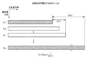
次に、上記説明したN本のマルチビームを用いる画像形成装置における各レーザビーム間の感光ドラム上での走査長差の検出および走査長差の補正方法を簡便かつ精度よく行う方法について具体的に説明する。図10Bは、走査長差の補正を短時間で行う原理を説明する図である。 Next, a specific example of a method for easily and accurately performing a method of detecting a scanning length difference on a photosensitive drum between laser beams and correcting a scanning length difference in the image forming apparatus using N multi-beams described above. explain. FIG. 10B is a diagram for explaining the principle of correcting the scanning length difference in a short time.
マルチビームの走査長差を補正する際に、N本のマルチビームの各ビームによって形成される走査長を上記説明した原理に基づいて測定して走査長差を補正するのが最も正確である。しかしながら、この補正方法では、N本のマルチビーム全てのパターンを形成し、各パターンごとに走査方向の先端および後端の位置を検出し、検出した各ビームの走査長から各ビーム間の走査長差を算出して補正を行わなければならない。そのため、各ビームパターンの形成時間は長くなりトナー量も増える。またパターン検出時間や補正処理時間も長くなるという欠点がある。 When correcting the multi-beam scanning length difference, it is most accurate to correct the scanning length difference by measuring the scanning length formed by each of the N multi-beams based on the principle described above. However, in this correction method, all N multi-beam patterns are formed, the positions of the front and rear ends in the scanning direction are detected for each pattern, and the scanning length between each beam is determined from the detected scanning length of each beam. The difference must be calculated and corrected. For this reason, the time for forming each beam pattern becomes longer and the amount of toner also increases. In addition, there is a disadvantage that the pattern detection time and the correction processing time become long.
そこで、本画像形成装置では、図10Bに示すように、N本のマルチビームのうち走査長差の補正に用いる形成パターンを副走査方向に配列されたビームの両端に位置するビームL1(1ライン目)とLN(Nライン目)の2本のみに限定する。次に、フォトセンサで形成されたパターンL1、LNの主走査方向の先端および後端を読み取り、上記説明した(1)式で、図10Bに模式的に示した1ライン目とNライン目の走査長差ΔLNを算出する。また、Liラインの走査長差ΔLiは、Liラインのパターンを形成せずに、例えば、ΔLNを比例配分した下記の(2)式、
ΔLi=ΔLN×i/(N−1) (2)
で算出する。この結果、パターン形成時間が短縮でき、トナー量が削減でき、さらに、パターンを検出時間や補正処理時間も削減することができるので、走査長差の補正方法を簡便かつ精度よく実現することができる。
Therefore, in the present image forming apparatus, as shown in FIG. 10B, a beam L1 (one line) positioned at both ends of the beam arranged in the sub-scanning direction is used for correcting the scanning length difference among the N multi-beams. Eyes) and LN (Nth line). Next, the leading and trailing edges of the patterns L1 and LN formed by the photosensor in the main scanning direction are read, and the first and Nth lines schematically shown in FIG. The scanning length difference ΔLN is calculated. In addition, the Li line scanning length difference ΔLi is, for example, the following equation (2) in which ΔLN is proportionally distributed without forming the Li line pattern:
ΔLi = ΔLN × i / (N−1) (2)
Calculate with As a result, the pattern formation time can be shortened, the amount of toner can be reduced, and the pattern detection time and correction processing time can also be reduced, so that a method for correcting the scanning length difference can be realized easily and accurately. .
本実施形態では、画像形成動作を行う前に所定のタイミングで中間転写ベルト31上に上記説明したレジストレーション補正用パターン画像601を形成し、次に、レジストレーション補正用フォトセンサ60a、60bで形成したパターン画像601を読み取る。次に、読み取った画像に基づいて各色に相当する感光体ドラム上でのレジストレーションずれを検出し、次に、検出結果に基づいて補正量を算出する。最後に、得られた補正量に基づいて記録されるべき画像信号に電気的な補正をかけ、及び/又は、レーザビーム光路中に設けられている折り返しミラー16aを駆動して、光路長変化或いは光路変化の補正を行う。
In the present embodiment, the registration
以下、上記説明した処理のフローチャートを図10Cに示す。 A flowchart of the above-described processing is shown in FIG. 10C.
図10Cのフローチャートを用いて、本画像形成装置による走査長差の補正方法を説明する。この処理は、ROMに格納された制御プログラムがRAMを作業領域に用いながら各部を制御して実行するものである。 A method of correcting the scanning length difference by the image forming apparatus will be described with reference to the flowchart of FIG. 10C. This process is executed by a control program stored in the ROM controlling each unit while using the RAM as a work area.
まず、ステップS100において、N本のマルチビームを用いる場合、副走査方向に配列されたビームの両端に位置する1ライン目とNライン目のみのビームを用いて補正用パターンL1、LN(図8)を感光体ドラム上に形成する。 First, in the case where N multi-beams are used in step S100, correction patterns L1 and LN (FIG. 8) are performed using only the first and N-th beams positioned at both ends of the beams arranged in the sub-scanning direction. ) On the photosensitive drum.
次に、ステップS110において、フォトセンサで、中間転写ベルト31上転写されたパターンL1、LNの主走査方向の先端および後端の位置(図9)を検出する。
Next, in step S110, the positions of the leading and trailing ends (FIG. 9) in the main scanning direction of the patterns L1 and LN transferred on the
次に、ステップS120において、検出されたパターンL1、LNの主走査方向の先端および後端の位置から1ライン目とNライン目の走査長差ΔLNを(1)式を用いて算出する。 Next, in step S120, the scanning length difference ΔLN for the first line and the N-th line is calculated using the equation (1) from the positions of the leading and trailing ends of the detected patterns L1, LN in the main scanning direction.
次に、ステップS130において、ステップS120で算出されたΔLNを次式で比例配分して、iライン目の走査長差ΔLiを算出する。 Next, in step S130, ΔLN calculated in step S120 is proportionally distributed by the following equation to calculate a scanning length difference ΔLi for the i-th line.
ΔLi=ΔLN×i/(N−1)
次に、ステップS140において、算出された走査長差ΔLiを用いて各ビームの走査長差を補正する。
ΔLi = ΔLN × i / (N−1)
Next, in step S140, the scanning length difference of each beam is corrected using the calculated scanning length difference ΔLi.
(4本のマルチビームを用いる場合の例:図10D)
従って、4本のマルチビームを用いる場合には、図10Dに示すように、1ライン目と4ライン目のみのパターンL1、L4を感光体ドラム上に形成する。次に、フォトセンサで中間転写ベルト31上に転写されたパターンL1、L4の主走査方向の先端および後端の位置を検出する。その結果、(1)式でΔL4が算出でき、2ライン目と3ライン目の走査長差は、下式で算出することができるので、これらの値を用いて走査長差を補正することができる。
(Example of using four multi-beams: FIG. 10D)
Therefore, when four multi-beams are used, patterns L1 and L4 for only the first and fourth lines are formed on the photosensitive drum as shown in FIG. 10D. Next, the positions of the leading and trailing ends of the patterns L1 and L4 transferred on the
ΔL2=ΔL4×(1/3)
ΔL3=ΔL4×(2/3)
(走査長差を検出する方法:図11)
次に、上記説明したマルチビームによる感光体上の走査長差の検出方法について4本のマルチビームを例に詳細に説明する。レーザビーム間の主走査長差を検知するためのパターンには各色の主走査倍率補正用パターンと同形状のものを用いる。このパターンは、両端のレーザビーム(LD1とLD4)の各々の主走査長差を検知するためLD1とLD4の各々のレーザビームで形成することになる。パターン形成時は、副走査方向の形成速度(感光ドラムの回転速度および中間転写ベルトの搬送スピード)を1/(ビーム数)にすることで、通常の画像形成時と同じ副走査方向の解像度が得られることになる。本実施形態では4ビームであるため、副走査方向の形成速度を1/4にしている。パターン検知後の主走査長差は、各色間の主走査倍率誤差と同様の計算で算出することができる。
ΔL2 = ΔL4 × (1/3)
ΔL3 = ΔL4 × (2/3)
(Method of detecting the scanning length difference: FIG. 11)
Next, the above-described method for detecting the scanning length difference on the photosensitive member by the multi-beam will be described in detail by taking four multi-beams as an example. The pattern for detecting the main scanning length difference between the laser beams has the same shape as the main scanning magnification correction pattern for each color. This pattern is formed by the laser beams of LD1 and LD4 in order to detect the main scanning length difference between the laser beams (LD1 and LD4) at both ends. During pattern formation, the resolution in the sub-scanning direction (the rotational speed of the photosensitive drum and the conveyance speed of the intermediate transfer belt) is set to 1 / (number of beams) so that the resolution in the sub-scanning direction is the same as in normal image formation. Will be obtained. In this embodiment, since there are four beams, the formation speed in the sub-scanning direction is ¼. The main scanning length difference after pattern detection can be calculated by the same calculation as the main scanning magnification error between colors.
LD1〜LD4の主走査長差であるが、図11に示すように感光ドラム上に照射されるLD1〜LD4のレーザビームは微小間隔(例えば、解像度600dpiの場合の間隔は、42.3μm)で感光ドラム11上に照射される。ここで、入射角が大きくなければ(45度未満)、隣り合うビーム間の光路長差(ΔA、ΔB、ΔC)はほぼ等しいものになる。このため、LD1とLD4の主走査長差がΔLであったとすると、LD1-LD2間、LD2-LD3間、LD3-LD4間の主走査長差は、それぞれほぼ1/3*ΔLとなる。なお、入射角が大きい場合(45度以上)には、感光ドラムの径と入射角とレーザビーム間隔の関係から計算もしくは所定のテーブルを用いて主走査長差を算出することができる。
The main scanning length difference between LD1 to LD4 is as follows. As shown in FIG. 11, the laser beams of LD1 to LD4 irradiated onto the photosensitive drum are at a very small interval (for example, the interval at a resolution of 600 dpi is 42.3 μm). Irradiated onto the
(本実施形態の主走査長差の補正例)
(各レーザビーム間の主走査長差の補正方法:図13)
次に、上記説明した方法により算出された主走査長差を用いてマルチビームにおける各レーザビーム間の主走査長差を補正する方法を具体的に説明する。図13は、各レーザビーム間の主走査長差の補正に用いるレーザ制御部の構成の一例を示すブロック図である。
(Example of correction of main scanning length difference of this embodiment)
(Main scanning length difference correction method between laser beams: FIG. 13)
Next, a method for correcting the main scanning length difference between the laser beams in the multi-beam using the main scanning length difference calculated by the above-described method will be specifically described. FIG. 13 is a block diagram illustrating an example of a configuration of a laser control unit used for correcting a main scanning length difference between laser beams.
光学系13は4つのレーザダイオード1001、ポリゴンミラー1002、ポリゴンモータ1003、ポリゴン制御部1004、f−θレンズ1009からなる。レーザダイオード1001から照射されたレーザ光は、回転駆動するポリゴンモータ1003によって、図中矢印方向に回転するポリゴンミラー1002によって走査される。次に、レーザ光はf-θレンズ1009によって周知のf−θ補正され、折り返しミラー16を介して感光ドラム11に照射される。また、ポリゴンモータ制御部1004はポリゴンモータ1003を所定回転で正確に回転するための制御部である。BDセンサ1005はレーザ光の1ラインの走査開始位置近傍に設けられ、レーザ光のライン走査(BD信号)を検出し、画像信号タイミング制御部1006に入力される。
The
(画像信号タイミング制御部:図14)
画像信号タイミング制御部1006の詳細を図14に示す。
(Image signal timing control unit: FIG. 14)
Details of the image signal
画像信号タイミング制御部1006は、図14に示すように、セレクタ1100、FIFO(First In First Out memory)1101〜1104、およびBDディレイ回路1105を有する。セレクタ1100には画像信号が入力され、入力された画像信号を1ライン毎に切り替え、FIFO(First In First Out memory)1101〜1104に入力する。BDディレイ回路1105は、BDセンサ1005から送られてくるBD信号を各レーザダイオードの主走査書き出しタイミングに応じて、BDセンサ36の出力の取り込みを遅延させる。この遅延量は4つのレーザビームが感光ドラム11上での主走査方向の物理的な位置ずれ量に応じて決定される。FIFO1101〜1104はラインメモリーであり、不図示の画像信号生成部より入力される4つのレーザダイオードに対応した画像データをBDディレイ回路1100からのタイミング信号に基づいて変調部1007に出力する。
As illustrated in FIG. 14, the image signal
(変調部:図15)
一方、図13において、センサ60からのパターン検知出力は補正量算出部1010に入力され、補正量算出部1010では各レーザビームの主走査長差補正量を変調部1007に出力する。変調部1007は、図15に示すように、PLL回路1201と、分周回路1202と、変調回路1203と、出力回路1204と、カウンタ回路1205とを有する。PLL回路1201は、基本クロック(基本CLK)を入力とし、この基本クロックのn倍の高周波クロックを出力する。この高周波クロックは、分周回路1202、出力回路1204にそれぞれ入力される。
(Modulation unit: FIG. 15)
On the other hand, in FIG. 13, the pattern detection output from the
(分周回路の出力:図16)
変調部1007の分周回路1202は、入力された高周波クロックをx回に一度カウントすることにより、入力された高周波クロックを1/x分周したクロックであるメインクロックを出力する(図16参照)。ここで、xは整数であればいくつでもかまわない。また、ここでは、説明の便宜のため、1/n分周しPLL回路1201に入力される基本クロックと同じ周期のメインクロックを出力すると仮定する。分周回路61から出力されるクロックは、カウンタ回路1205に入力される。
(Output of divider circuit: Fig. 16)
The
(変調回路の出力:図17)
変調部1007の変調回路1203は、後述するクロック信号に同期して、画像信号を変調する。通常、レーザの階調性を表すために、単位時間内での点灯時間をPWM変調で制御することが行われているので、本実施形態では、PWM変調(特にデジタルPWM変調)を行うものとして説明する。例えば、Aビットの画像信号をPWM変調する場合、この画像信号は2Aのパルス幅データに変換される。ここで、2Aのパルス幅データは(3)式を満たすように定数が決められている。
2A=n (3)
この変調回路1203は、画像信号からパルス幅データを生成し、このパルス幅データを出力回路1204に出力する(図17を参照)。
(Output of modulation circuit: FIG. 17)
The
2A = n (3)
The
(出力回路の出力:図18)
変調部1007の出力回路1204は、変調回路1203から出力されたパルス幅データに応じて、PLL回路1201から出力された高周波クロックに同期したPWM信号、高周波クロックに同期したクロック信号を出力する。PWM信号はレーザドライバ1008に、クロック信号は画像処理部(図示せず)および変調回路1203にそれぞれ出力される(図18の(a)クロック信号出力、(d)パルス幅データ、および(e)PWM信号を参照)。
(Output circuit output: Fig. 18)
The
カウンタ回路1205は、分周回路1202から出力されたクロック(高周波クロックを1/n分周したクロック)をカウントする(図18の(b)カウント値を参照)。カウンタ回路1205は、そのカウント値が設定された値に達すると、所定の信号を出力回路1204に出力する(図18の(b)カウント値および(c)カウンタ出力を参照)。ここで、カウンタ回路1205に設定された値は、上記(1)式で求められた値に応じて決定された値である。
The
このカウンタ回路1205が上記所定の信号を出力回路1204に出力すると、出力回路1204は、通常と異なる動作を行う。すなわち、通常動作においては、n個の高周波クロックでPWM信号、クロック信号の1つの周期を生成していたのに対し、上記所定の信号を入力した際には、上記周期と異なる周期のPWM信号、クロック信号を出力する(図18参照)。
When the
(出力回路の構成:図19)
次に、上記出力回路1204の具体的な構成について説明する。図19は図15の出力回路1204の詳細な構成を示すブロック図である。出力回路1204は、図19に示すように、変調制御部80と、9つのDタイプのフリップフロップ81a〜81iと、9つの2入力AND回路82a〜82iと、2つの2入力セレクタ回路83、84と、9入力OR回路86と、2入力OR回路87とを含む。
(Configuration of output circuit: FIG. 19)
Next, a specific configuration of the
変調回路1203は、入力された画像信号を8ビットのパルス幅データに変調する。このパルス幅データの各ビットは、2入力AND回路82a〜82iの入力の一方に入力される。ここで、2入力AND回路82hおよび82iには、同じデータが入力される。
The
フリップフロップ81a〜81iは、高周波クロック(CLK)の立ち上がりでD端子の入力をQ端子に出力する。各フリップフロップ81a〜81iの出力は、上記2入力AND回路82a〜82iの入力の他方に接続される。それと同時に各フリップフロップ81a〜81iは、フリップフロップ81aの出力がフリップフロップ81bの入力に、フリップフロップ81bの出力がフリップフロップ81cの入力にというような縦続に接続されている。また、フリップフロップ81hの出力は2入力セレクタ回路83および2入力セレクタ回路84にも接続される。フリップフロップ81iの出力は、2入力セレクタ回路83にも接続される。
The flip-
2入力AND回路82a〜82iの出力は、それぞれ9入力OR回路86に接続され、9入力OR回路86の出力はPWM信号として出力される。2入力セレクタ回路83は、変調制御部80の出力に応じて、フリップフロップ81h〜81iの出力を選択し、2入力OR回路87の入力の一方に接続される。2入力セレクタ回路84の他方の入力はGNDに接続されている。2入力セレクタ回路84は、変調制御部80の出力によって、フリップフロップ81hの出力をフリップフロップ81iに入力させるか否かを制御する。
The outputs of the 2-input AND
変調制御部80は、カウンタ回路64の出力に応じて、2入力セレクタ回路83、84のセレクト動作を切り換える。2入力OR回路87の入力の他方には、タイミング信号が入力され、2入力OR回路87の出力はフリップフロップ81aに入力される。
The
(出力回路の動作:図20)
次に、出力回路1204の動作について図20を参照しながら説明する。図20は図15の出力回路1204の動作例を示すタイミングチャートである。2入力OR回路87には、フリップフロップ81a〜81iに入力される高周波クロック(CLK)に同期してタイミング信号が入力される。このタイミング信号は、高周波クロックの1クロック分の幅の信号である。これにより、フリップフロップ81a〜81iで構成されるリングのシフトレジスタの出力の1つが常に"1"となる。
(Operation of output circuit: FIG. 20)
Next, the operation of the
変調制御部80では、カウンタ回路64の出力を受け、上記リング状のシフトレジスタの大きさ(すなわちリング状シフトレジスタを構成するフリップフロップの数)を制御するように2入力セレクタ回路83、84の動作を切り換える。1画素を8個の高周波クロック(CLK)で構成する場合は、2入力セレクタ回路83によりフリップフロップ81hの出力を選択し、2入力セレクタ回路84によりGNDを選択する。1画素を9個の高周波クロック(CLK)で構成する場合は、2入力セレクタ回路83によりフリップフロップ81iの出力を選択し、2入力セレクタ回路84によりフリップフロップ81hの出力を選択する。これらの切換で、フリップフロップ81a〜81iの出力として、8/9の高周波クロック(CLK)に1回"1"が出力されるようになる。
The
2入力OR回路82a〜82iにはパルス幅データが設定されており、そのパルス幅データは、1画素(=8/9CLK)毎に変化する。そして、各2入力AND回路82a〜82iにおいて、設定されたデータと8/9個の高周波クロック(CLK)に1度の"1"とのAND演算が行われ、9入力OR回路86において、各2入力OR回路82a〜82iのAND出力がOR演算される。このOR演算の結果として、8/9個の高周波クロック(CLK)で構成されたPWM信号が出力される。
Pulse width data is set in the 2-input OR
なお、図示しないが、これと同じ構成を使用し、画像データに相当するところに画像クロックのパターンを入力して、PWM信号と同様に8/9個の高周波クロック(CLK)で構成されたクロック信号を出力することができる。また、フリップフロップ81a〜81iの特定箇所(例えば81aと81e)の出力をJKフリップフロップ回路に入力することによって、PWM信号と同様に8/9個の高周波クロック(CLK)で構成されたクロック信号を出力することができる。
Although not shown in the figure, a clock composed of 8/9 high-frequency clocks (CLK) is used in the same way as the PWM signal, using the same configuration as this, inputting the pattern of the image clock to the location corresponding to the image data. A signal can be output. Further, by inputting the outputs of specific locations (for example, 81a and 81e) of the flip-
以上により、図20に示すように、1周期(画像有効エリア)内の特定箇所(書込み位置)で1画素の構成数を9個の高周波クロック(CLK)に、その他のときには、8個の高周波クロック(CLK)になるように制御する。この制御により、感光ドラム11面上の各レーザビームの走査長差が電気的に補正され、4つのレーザ光による走査長を互いに等しくすることが可能になる。なお、本実施形態では、1画素を構成する幅を変化させる特定箇所を、カウンタ回路64で決定しているが、例えば別のタイマー手段などで決定してもよい。
As described above, as shown in FIG. 20, the number of components of one pixel is set to nine high-frequency clocks (CLK) at a specific location (writing position) in one cycle (image effective area), and eight high-frequency clocks at other times. Control is performed so that the clock (CLK) is obtained. By this control, the scanning length difference of each laser beam on the surface of the
以上説明したように、本実施形態の画像形成装置では、感光体ドラム上へのレーザ光の走査入射角が各ビームによって異なる場合でも、走査入射角の差異によって生じる各ビームの主走査倍率の変動を上記のように簡単に補正することにより画質低下を低減することができる。 As described above, in the image forming apparatus according to the present embodiment, even when the scanning incident angle of the laser beam on the photosensitive drum is different for each beam, the fluctuation in the main scanning magnification of each beam caused by the difference in the scanning incident angle. Is easily corrected as described above, image quality deterioration can be reduced.
<本実施形態の画像形成装置の変形例>
次に、他の実施形態の画像形成装置について説明する。なお、本実施形態の画像形成装置は上記説明した上記実施形態の画像形成装置と類似する装置であるので、以下の説明では、本実施形態の画像形成装置が上記実施形態の画像形成装置と異なる点についてのみ説明するものとする。
<Modification of Image Forming Apparatus According to Embodiment>
Next, an image forming apparatus according to another embodiment will be described. The image forming apparatus according to the present embodiment is an apparatus similar to the image forming apparatus according to the above-described embodiment. Therefore, in the following description, the image forming apparatus according to the present embodiment is different from the image forming apparatus according to the above-described embodiment. Only the point will be described.
(本実施形態の画像形成装置の特徴:図12)
本実施形態の画像形成装置では、図12に一例を示すレーザビームが主走査方向および副走査方向の両方に複数配置された面発光タイプのマルチビームを用い、このマルチビームを使用する場合の主走査長差を補正する補正処理ができることを特徴としている。
(Characteristics of the image forming apparatus of this embodiment: FIG. 12)
In the image forming apparatus according to the present embodiment, a surface emission type multi-beam in which a plurality of laser beams shown in FIG. 12 are arranged in both the main scanning direction and the sub-scanning direction is used, and the main beam when this multi-beam is used. It is characterized in that a correction process for correcting the scanning length difference can be performed.
図12の例では、主走査方向に4列、副走査方向に4列で合計16個のレーザビームを有する。図中の矢印は走査方向を表す。主走査方向に配置(配列)された4つのビーム(例えば、LD11、LD12、LD13、LD14)は、副走査方向に所定ピッチ(例えば1200dpi=21.2μm)で並んでおり、主走査方向には、所定ピッチ(例えばΔL2)で並んでいる。主走査方向に配置(配列)された他の4つのビーム(例えば、LD21、LD22、LD23、LD24)も同様である。また、副走査方向に配置(配列)された4つのビーム(例えばLD11、LD21、LD31、LD41)は図に示すように副走査方向に所定ピッチ(例えば21.2μm×4=84.7μm )で並んでいる。副走査方向に配置(配列)された他の4つのビーム(例えばLD12、LD22、LD32、LD42)も同様である。このため、16個のレーザビームの副走査方向の走査間隔は全て1200dpi=21.2μm となっている。 In the example of FIG. 12, a total of 16 laser beams are provided in four rows in the main scanning direction and four rows in the sub-scanning direction. The arrow in the figure represents the scanning direction. Four beams (for example, LD11, LD12, LD13, and LD14) arranged (arranged) in the main scanning direction are arranged at a predetermined pitch (for example, 1200 dpi = 21.2 μm) in the sub-scanning direction. Are arranged at a predetermined pitch (for example, ΔL2). The same applies to the other four beams (for example, LD21, LD22, LD23, and LD24) arranged (arranged) in the main scanning direction. Further, four beams (for example, LD11, LD21, LD31, and LD41) arranged (arranged) in the sub-scanning direction have a predetermined pitch (for example, 21.2 μm × 4 = 84.7 μm) in the sub-scanning direction as shown in the figure. Are lined up. The same applies to the other four beams (for example, LD12, LD22, LD32, and LD42) arranged (arranged) in the sub-scanning direction. For this reason, all the scanning intervals of the 16 laser beams in the sub-scanning direction are 1200 dpi = 21.2 μm.
上記のような16個のレーザビームを用いる場合のレジストレーション補正用パターンとしては、トナー、検出時間および補正処理時間の短縮のため1ライン目と16ライン目のパターンのみを形成する。すなわち、図12の副走査方向で両端部に配置されるLD14(1ライン目)とLD41(16ライン目)のみによってトナー像が形成されるようなパターンを形成する。ここで、LD14とLD41の副走査方向のピッチ間隔は、21.2μm×15=317.5μmである。隣り合うビーム間の光路長差はほぼ等しいと考えられるため、LD14とLD41の主走査長差がΔL1であったとすると、LD14-LD13間、LD13-LD12間、・・・LD42-LD41間の主走査長差はすべてほぼ1/15*ΔL1となる。そこで、この1ライン目〜16ライン目までの主走査長差(すべてほぼ1/15*ΔL1)を用い、前述の実施形態で説明した補正方法により、各ビームの主走査倍率(走査長差)の補正を簡単かつ正確に行うことができる。 As the registration correction pattern in the case of using 16 laser beams as described above, only the patterns for the first line and the 16th line are formed in order to shorten the toner, the detection time, and the correction processing time. That is, a pattern is formed such that a toner image is formed only by LD 14 (first line) and LD 41 (16th line) arranged at both ends in the sub-scanning direction of FIG. Here, the pitch interval between the LD 14 and the LD 41 in the sub-scanning direction is 21.2 μm × 15 = 317.5 μm. Since the optical path length difference between adjacent beams is considered to be substantially equal, if the main scanning length difference between LD14 and LD41 is ΔL1, the main path between LD14 and LD13, between LD13 and LD12,. All the scanning length differences are approximately 1/15 * ΔL1. Accordingly, the main scanning magnification difference (scanning length difference) of each beam is obtained by using the correction method described in the above-described embodiment, using the main scanning length difference from the first line to the 16th line (all approximately 1/15 * ΔL1). Can be corrected easily and accurately.
なお、主走査長差の精度を上げるために主走査方向に並んでいる4つごと(LD11〜LD14、LD21〜LD24、LD31〜LD34、LD41〜LD44)に補正を行ってもかまわない。すなわち、LD11〜LD14のグループでは副走査方向の両端に配置されているLD11とLD14の各々のみで主走査長補正用パターンを形成する。隣り合うビーム間の光路長差はほぼ等しいと考えられるため、LD11とLD14の主走査長差がΔL2であったとすると、LD11-LD14間の主走査長差はすべてほぼ1/3*ΔL2となる。同様にLD21〜LD24、LD31〜LD34、LD41〜LD44においても副走査方向の両端に配置されているLD21とLD24、LD31とLD34、LD41とLD44の各々のみで主走査長補正用パターンを形成する。各々の検知結果の1/3がそのレーザビーム間に配置される、隣り合うレーザビーム間の主走査長差となる。そこで、以上の検知結果を元に、前述の実施形態で説明した補正方法を用いることで面発光タイプでの主走査長補正を精度よく簡単に行うことができる。 In order to improve the accuracy of the main scanning length difference, correction may be performed for every four (LD11 to LD14, LD21 to LD24, LD31 to LD34, and LD41 to LD44) arranged in the main scanning direction. That is, in the group of LD11 to LD14, the main scanning length correction pattern is formed only by each of LD11 and LD14 arranged at both ends in the sub-scanning direction. Since the optical path length difference between adjacent beams is considered to be substantially equal, if the main scanning length difference between LD11 and LD14 is ΔL2, all the main scanning length differences between LD11 and LD14 are approximately 1/3 * ΔL2. . Similarly, in LD21 to LD24, LD31 to LD34, and LD41 to LD44, the main scanning length correction pattern is formed only by each of LD21 and LD24, LD31 and LD34, and LD41 and LD44 arranged at both ends in the sub-scanning direction. One-third of each detection result is the main scanning length difference between adjacent laser beams arranged between the laser beams. Therefore, based on the above detection results, the main scanning length correction in the surface emission type can be easily performed with high accuracy by using the correction method described in the above embodiment.
本実施形態においては補正手段としてメインクロックを構成する高周波クロックの個数を変える書込み位置を制御する手段を用いていた。しかしながら、各レーザビームで画像を形成するための画像クロックをPLL制御を用いた周波数変調方式にする手段を用いるように変更しても同様の効果が得られる。このように変更した場合には、図13の構成は変わらないが、画像信号タイミング制御部1006と変調部1007の内部構成が異なる。変調部1007の構成の変更例は図示しないが、周知のパルス幅変調回路などで構成されることになる。
In the present embodiment, means for controlling the write position for changing the number of high-frequency clocks constituting the main clock is used as the correction means. However, the same effect can be obtained even if the image clock for forming an image with each laser beam is changed to use a means for frequency modulation using PLL control. In such a change, the configuration of FIG. 13 does not change, but the internal configurations of the image signal
(画像タイミング制御部:図21)
図21に画像タイミング制御部の構成を示す。
(Image timing control unit: FIG. 21)
FIG. 21 shows the configuration of the image timing control unit.
FIFO1101〜1104の画像信号読み出しタイミングを決定する画像クロックをCLK発生回路1106-1〜4によって生成する。CLK発生回路1106-1〜4は周知のPLL制御を用いた周波数変調回路からなり、外部の調整値で生成するCLKの周波数を決定する。この調整値は主走査長差の補正量によって算出される値が入力されることになる。
The CLK generation circuits 1106-1 to 110-4 generate image clocks for determining the image signal readout timing of the
以上説明したように、従来の画像形成装置の構成をあまり変更することなく、各ビームの主走査倍率の補正が簡単な構成で正確にできる。また、ビーム数が多くなっても主走査長差の補正構成の規模が大きくなることや補正時間が長くなることはない。 As described above, it is possible to accurately correct the main scanning magnification of each beam with a simple configuration without significantly changing the configuration of the conventional image forming apparatus. Further, even if the number of beams increases, the scale of the main scanning length difference correction configuration does not increase and the correction time does not increase.
尚、本発明の目的は、前述した実施形態の機能を実現するソフトウェアのプログラムコードを記録した記録媒体(または記憶媒体)でも達成できる。この場合、記録媒体をシステムあるいは装置に供給し、そのシステムあるいは装置のコンピュータ(またはCPUやMPU)が記録媒体に格納されたプログラムコードを読み出し実行することによっても、達成されることは言うまでもない。この場合、記録媒体から読み出されたプログラムコード自体が前述した実施形態の機能を実現することになり、そのプログラムコードを記録した記録媒体は本発明を構成することになる。 The object of the present invention can also be achieved by a recording medium (or storage medium) that records a program code of software that realizes the functions of the above-described embodiments. In this case, it goes without saying that this can also be achieved by supplying the recording medium to the system or apparatus and reading and executing the program code stored in the recording medium by the computer (or CPU or MPU) of the system or apparatus. In this case, the program code itself read from the recording medium realizes the functions of the above-described embodiment, and the recording medium on which the program code is recorded constitutes the present invention.
また、コンピュータが読み出したプログラムコードを実行することにより、前述した実施形態の機能が実現されるだけでなく、そのプログラムコードの指示に基づき、コンピュータ上で稼働しているオペレーティングシステム(OS)などが実際の処理の一部または全部を行い、その処理によって前述した実施形態の機能が実現される場合も含まれることは言うまでもない。 Further, by executing the program code read by the computer, not only the functions of the above-described embodiments are realized, but also an operating system (OS) running on the computer based on the instruction of the program code. It goes without saying that a case where the function of the above-described embodiment is realized by performing part or all of the actual processing and the processing is included.
さらに、記録媒体から読み出されたプログラムコードは、コンピュータに挿入された機能拡張カードやコンピュータに接続された機能拡張ユニットに備わるメモリに書込まれる。そこで、書込まれたプログラムコードの指示に基づき、その機能拡張カードや機能拡張ユニットに備わるCPUなどが実際の処理の一部または全部を行い、その処理によって前述した実施形態の機能が実現される場合も含まれることは言うまでもない。 Further, the program code read from the recording medium is written in a memory provided in a function expansion card inserted into the computer or a function expansion unit connected to the computer. Therefore, based on the instruction of the written program code, the CPU or the like provided in the function expansion card or function expansion unit performs part or all of the actual processing, and the functions of the above-described embodiments are realized by the processing. Needless to say, cases are also included.
又、自装置にセットされたCD−ROM、或いは、インターネット等の外部供給源から、前述した実施形態の機能を実現する為のプログラムデータを、自装置のメモリにダウンロードし、前述した実施形態の機能が実現されるような形態も本発明に包含される。 Also, program data for realizing the functions of the above-described embodiment is downloaded from the CD-ROM set in the own device or an external supply source such as the Internet to the memory of the own device, and A form in which the function is realized is also included in the present invention.
本発明を上記記録媒体に適用する場合、その記録媒体には、先に説明したフローチャート(図5、図6)に対応するプログラムコードが格納されることが好ましい。 When the present invention is applied to the above recording medium, the recording medium preferably stores program codes corresponding to the above-described flowcharts (FIGS. 5 and 6).
1R 画像読取部
1P 画像出力部
10 画像形成部
11a〜11d 感光ドラム
12a〜12d 一次帯電器
13a〜13d 光学系
16a〜16d 折り返しミラー
14a〜14d 現像部
20 給紙ユニット
30 中間転写ユニット
31 中間転写ベルト
60a、60b レジストレーション補正用のフォトセンサ
601 レジストレーション補正用パターン
801 副走査の書き出し位置と主走査傾きのずれ量の検知パターン
802 主走査の書き出し位置と主走査倍率のずれ量の検知パターン
1R image reading unit 1P
Claims (8)
前記感光体上を走査する前記複数のビームのうち前記回転方向の両端を走査するビームそれぞれにより前記感光体上に複数のトナーパターンが形成されるように前記画像形成手段を制御するパターン形成手段と、
前記感光体の回転方向の両端を走査するビームそれぞれにより形成された前記複数のトナーパターンを検出する検出手段と、
前記検出手段の検出結果に基づいて、前記複数のビームそれぞれによって形成される前記トナー像の前記所定の方向における長さが等しくなる様に、前記複数の光源それぞれからのビームを出射させるタイミングを制御する光源制御手段と、
前記画像形成手段が前記複数のトナーパターンを形成する際に前記感光体の回転速度を前記所定の回転速度よりも減速させる速度制御手段と、
を備えており、
前記トナー像は所定の解像度で形成され、
前記感光体上を走査する隣り合うビームの間隔が前記所定の解像度に応じた間隔になるように前記複数の光源は配列され、
前記複数のビームの数をNとした場合に、前記速度制御手段は、前記複数のトナーパターンが前記所定の解像度で形成されるように前記感光体の回転速度を1/Nに減速させることを特徴とする画像形成装置。 A plurality of light sources arranged to irradiate a plurality of beams on different positions on the photoconductor in a rotation direction of the photoconductor, and the plurality of beams on the photoconductor rotating at a predetermined rotation speed; An image forming apparatus comprising image forming means for forming an electrostatic latent image on the photoreceptor by scanning in a predetermined direction and developing the electrostatic latent image into a toner image,
Pattern forming means for controlling the image forming means so that a plurality of toner patterns are formed on the photosensitive member by beams that scan both ends in the rotation direction among the plurality of beams that scan on the photosensitive member; ,
Detecting means for detecting the plurality of toner patterns formed by the respective beams that scan both ends of the photosensitive member in the rotation direction;
Based on the detection results of the detection means, the timing for emitting the beams from the plurality of light sources is controlled so that the lengths of the toner images formed by the plurality of beams in the predetermined direction are equal. Light source control means for
A speed control means for decelerating the rotational speed of the photoreceptor below the predetermined rotational speed when the image forming means forms the plurality of toner patterns;
Equipped with a,
The toner image is formed with a predetermined resolution,
The plurality of light sources are arranged so that an interval between adjacent beams that scan on the photoconductor is an interval according to the predetermined resolution,
When the number of the plurality of beams is N, the speed control unit reduces the rotational speed of the photoconductor to 1 / N so that the plurality of toner patterns are formed with the predetermined resolution. An image forming apparatus.
前記感光体上を走査する前記複数のビームのうち前記回転方向の両端を走査するビームそれぞれにより前記感光体上に複数のトナーパターンが形成されるように前記画像形成手段を制御するパターン形成手段と、
前記感光体の回転方向の両端を走査するビームそれぞれにより形成された前記複数のトナーパターンを検出する検出手段と、
前記検出手段の検出結果に基づいて、前記複数のビームそれぞれによって形成される前記トナー像の前記所定の方向における長さが等しくなる様に、前記複数の光源それぞれからのビームを出射させるタイミングを制御する光源制御手段と、
前記画像形成手段が前記複数のトナーパターンを形成する際に前記感光体の回転速度を前記所定の回転速度よりも減速させる速度制御手段と、
を備えており、
前記画像形成手段は、
前記感光体の回転速度に同期するように回転駆動され、前記感光体上の前記トナー像が転写される中間転写体と、
前記中間転写体上に転写されたトナー像を記録媒体に転写する転写手段と、
を備えており、
前記検出手段は、前記中間転写体上に転写された前記複数のトナーパターンを検出し、
前記速度制御手段は、前記複数のトナーパターンを形成する際に前記中間転写体の回転速度を減速させ、
前記トナー像は所定の解像度で形成され、
前記感光体上を走査する隣り合うビームの間隔が前記所定の解像度に応じた間隔になるように前記複数の光源は配列され、
前記複数のビームの数をNとした場合に、前記速度制御手段は、前記感光体上の前記複数のトナーパターンが前記所定の解像度で前記中間転写体に転写されるように前記中間転写体の回転速度を1/Nに減速させることを特徴とする画像形成装置。 A plurality of light sources arranged to irradiate a plurality of beams on different positions on the photoconductor in a rotation direction of the photoconductor, and the plurality of beams on the photoconductor rotating at a predetermined rotation speed; An image forming apparatus comprising image forming means for forming an electrostatic latent image on the photoreceptor by scanning in a predetermined direction and developing the electrostatic latent image into a toner image,
Pattern forming means for controlling the image forming means so that a plurality of toner patterns are formed on the photosensitive member by beams that scan both ends in the rotation direction among the plurality of beams that scan on the photosensitive member; ,
Detecting means for detecting the plurality of toner patterns formed by the respective beams that scan both ends of the photosensitive member in the rotation direction;
Based on the detection results of the detection means, the timing for emitting the beams from the plurality of light sources is controlled so that the lengths of the toner images formed by the plurality of beams in the predetermined direction are equal. Light source control means for
A speed control means for decelerating the rotational speed of the photoreceptor below the predetermined rotational speed when the image forming means forms the plurality of toner patterns;
Equipped with a,
The image forming unit includes:
An intermediate transfer member that is rotationally driven to synchronize with the rotation speed of the photosensitive member and to which the toner image on the photosensitive member is transferred;
Transfer means for transferring the toner image transferred onto the intermediate transfer member to a recording medium;
With
The detecting means detects the plurality of toner patterns transferred onto the intermediate transfer member;
The speed control means reduces the rotational speed of the intermediate transfer member when forming the plurality of toner patterns,
The toner image is formed with a predetermined resolution,
The plurality of light sources are arranged so that an interval between adjacent beams that scan on the photoconductor is an interval according to the predetermined resolution,
When the number of the plurality of beams is N, the speed control unit is configured to transfer the plurality of toner patterns on the photosensitive member to the intermediate transfer member at the predetermined resolution. An image forming apparatus, wherein the rotational speed is reduced to 1 / N.
前記光源制御手段は、前記補正量に基づいて前記複数の光源それぞれからのビームを出射させるタイミングを制御することを特徴とする請求項3に記載の画像形成装置。 The light source control means calculates a scanning length difference in the predetermined direction of each of the beams forming the plurality of toner patterns based on the positions of the front and rear ends of the plurality of toner patterns detected by the detection means. And calculating means for calculating a correction amount for each of the plurality of beams so that the lengths of the toner images formed by the plurality of beams in the predetermined direction are equal based on the scanning length difference. With
The image forming apparatus according to claim 3, wherein the light source control unit controls a timing of emitting a beam from each of the plurality of light sources based on the correction amount.
Priority Applications (3)
| Application Number | Priority Date | Filing Date | Title |
|---|---|---|---|
| JP2005267694A JP4804082B2 (en) | 2005-09-14 | 2005-09-14 | Image forming apparatus |
| US11/531,731 US7382390B2 (en) | 2005-09-14 | 2006-09-14 | Image forming apparatus and control method thereof having main scan length correcting feature |
| US12/047,965 US7652684B2 (en) | 2005-09-14 | 2008-03-13 | Image forming apparatus and control method thereof having main scan length correcting feature |
Applications Claiming Priority (1)
| Application Number | Priority Date | Filing Date | Title |
|---|---|---|---|
| JP2005267694A JP4804082B2 (en) | 2005-09-14 | 2005-09-14 | Image forming apparatus |
Publications (3)
| Publication Number | Publication Date |
|---|---|
| JP2007076198A JP2007076198A (en) | 2007-03-29 |
| JP2007076198A5 JP2007076198A5 (en) | 2008-10-30 |
| JP4804082B2 true JP4804082B2 (en) | 2011-10-26 |
Family
ID=37854613
Family Applications (1)
| Application Number | Title | Priority Date | Filing Date |
|---|---|---|---|
| JP2005267694A Expired - Fee Related JP4804082B2 (en) | 2005-09-14 | 2005-09-14 | Image forming apparatus |
Country Status (2)
| Country | Link |
|---|---|
| US (2) | US7382390B2 (en) |
| JP (1) | JP4804082B2 (en) |
Families Citing this family (12)
| Publication number | Priority date | Publication date | Assignee | Title |
|---|---|---|---|---|
| JPH0249354A (en) * | 1988-08-11 | 1990-02-19 | Matsushita Electric Ind Co Ltd | Manufacture of anode plate for sealed elad-acid battery |
| JP4804082B2 (en) * | 2005-09-14 | 2011-10-26 | キヤノン株式会社 | Image forming apparatus |
| JP5127298B2 (en) * | 2007-05-22 | 2013-01-23 | キヤノン株式会社 | Image forming apparatus and curvature correction data calculation method |
| JP4379508B2 (en) * | 2007-09-11 | 2009-12-09 | コニカミノルタビジネステクノロジーズ株式会社 | Image forming apparatus, gradation correction method, and gradation correction program |
| JP5070559B2 (en) * | 2008-09-16 | 2012-11-14 | 株式会社リコー | Optical scanning apparatus and image forming apparatus |
| JP5812669B2 (en) * | 2011-04-27 | 2015-11-17 | キヤノン株式会社 | Image processing apparatus, image processing method, and computer program. |
| US9924105B2 (en) * | 2011-12-12 | 2018-03-20 | Visys Nv | System and method for individually inspecting objects in a stream of products and a sorting apparatus comprising such system |
| JP6150698B2 (en) * | 2013-09-25 | 2017-06-21 | キヤノン株式会社 | Image forming apparatus and control method thereof |
| JP6349883B2 (en) * | 2014-03-31 | 2018-07-04 | ブラザー工業株式会社 | Image forming apparatus, forming condition adjusting method, and forming condition adjusting program |
| JP6164139B2 (en) * | 2014-03-31 | 2017-07-19 | ブラザー工業株式会社 | Image forming apparatus, forming condition adjusting method, and storage medium storing forming condition adjusting program |
| US9691211B2 (en) | 2014-07-03 | 2017-06-27 | Seiko Epson Corporation | Image processing apparatus, image processing method, and program |
| US10761467B1 (en) * | 2019-08-27 | 2020-09-01 | Toshiba Tec Kabushiki Kaisha | Image forming apparatus and image position adjustment method |
Family Cites Families (10)
| Publication number | Priority date | Publication date | Assignee | Title |
|---|---|---|---|---|
| JP3129810B2 (en) * | 1992-01-27 | 2001-01-31 | 大日本スクリーン製造株式会社 | Image recording apparatus and image recording method |
| JP3209810B2 (en) * | 1992-11-25 | 2001-09-17 | 株式会社リコー | Optical scanning device |
| US6185026B1 (en) * | 1998-08-06 | 2001-02-06 | Ricoh Company, Ltd. | Multi-beam scanning apparatus |
| JP2000155277A (en) * | 1998-11-20 | 2000-06-06 | Asahi Optical Co Ltd | Multibeam scanning optical device |
| JP2000218858A (en) * | 1999-01-29 | 2000-08-08 | Canon Inc | Image forming apparatus |
| JP4141056B2 (en) | 1999-06-25 | 2008-08-27 | 株式会社リコー | Multi-beam image forming apparatus |
| JP2004102103A (en) * | 2002-09-12 | 2004-04-02 | Canon Inc | Image forming apparatus and method for controlling scanning length thereof |
| JP2004302062A (en) * | 2003-03-31 | 2004-10-28 | Canon Inc | Multibeam light scanner |
| JP4323939B2 (en) * | 2003-12-11 | 2009-09-02 | キヤノン株式会社 | Image forming apparatus and image forming method |
| JP4804082B2 (en) * | 2005-09-14 | 2011-10-26 | キヤノン株式会社 | Image forming apparatus |
-
2005
- 2005-09-14 JP JP2005267694A patent/JP4804082B2/en not_active Expired - Fee Related
-
2006
- 2006-09-14 US US11/531,731 patent/US7382390B2/en not_active Expired - Fee Related
-
2008
- 2008-03-13 US US12/047,965 patent/US7652684B2/en not_active Expired - Fee Related
Also Published As
| Publication number | Publication date |
|---|---|
| US7652684B2 (en) | 2010-01-26 |
| US20080166140A1 (en) | 2008-07-10 |
| JP2007076198A (en) | 2007-03-29 |
| US7382390B2 (en) | 2008-06-03 |
| US20070057989A1 (en) | 2007-03-15 |
Similar Documents
| Publication | Publication Date | Title |
|---|---|---|
| JP4804082B2 (en) | Image forming apparatus | |
| JP2013240994A (en) | Image forming apparatus for correcting displacement between laser beams | |
| US20020085081A1 (en) | Image forming apparatus for maintaining a constant beam scanning state | |
| JP2006035725A (en) | Color imaging device and process cartridge | |
| US6281922B1 (en) | Image forming apparatus | |
| JP5354891B2 (en) | Image forming apparatus | |
| JP2004004510A (en) | Optical scanning apparatus and image forming apparatus | |
| JP3768942B2 (en) | Image forming apparatus | |
| US10915994B2 (en) | Image forming apparatus | |
| JP6726046B2 (en) | Image forming device | |
| JP2009151286A (en) | Image forming apparatus and method, program and recording medium | |
| JP6700970B2 (en) | Image forming device | |
| JP6486430B2 (en) | Image forming apparatus for correcting misalignment between laser beams | |
| JP4424230B2 (en) | Image forming apparatus | |
| JP4423152B2 (en) | Image forming apparatus | |
| JP2006130740A (en) | Image forming apparatus and method of forming image | |
| JP2009175470A (en) | Optical scanner and image forming apparatus equipped with the same | |
| JP3951519B2 (en) | Multicolor image forming apparatus and multicolor image forming method | |
| JP6758906B2 (en) | Image forming device | |
| JP2002023589A (en) | Image forming device | |
| JP2004258126A (en) | Image forming apparatus and its image writing start position adjusting method | |
| JP4337801B2 (en) | Image forming apparatus and exposure control method thereof | |
| JP2006159502A (en) | Image forming device | |
| JP2006150666A (en) | Image forming device | |
| JP2019130723A (en) | Color image formation apparatus |
Legal Events
| Date | Code | Title | Description |
|---|---|---|---|
| A521 | Request for written amendment filed |
Free format text: JAPANESE INTERMEDIATE CODE: A523 Effective date: 20080916 |
|
| A621 | Written request for application examination |
Free format text: JAPANESE INTERMEDIATE CODE: A621 Effective date: 20080916 |
|
| A977 | Report on retrieval |
Free format text: JAPANESE INTERMEDIATE CODE: A971007 Effective date: 20110204 |
|
| A131 | Notification of reasons for refusal |
Free format text: JAPANESE INTERMEDIATE CODE: A131 Effective date: 20110210 |
|
| A521 | Request for written amendment filed |
Free format text: JAPANESE INTERMEDIATE CODE: A523 Effective date: 20110408 |
|
| A131 | Notification of reasons for refusal |
Free format text: JAPANESE INTERMEDIATE CODE: A131 Effective date: 20110523 |
|
| A521 | Request for written amendment filed |
Free format text: JAPANESE INTERMEDIATE CODE: A523 Effective date: 20110613 |
|
| TRDD | Decision of grant or rejection written | ||
| A01 | Written decision to grant a patent or to grant a registration (utility model) |
Free format text: JAPANESE INTERMEDIATE CODE: A01 Effective date: 20110805 |
|
| A01 | Written decision to grant a patent or to grant a registration (utility model) |
Free format text: JAPANESE INTERMEDIATE CODE: A01 |
|
| A61 | First payment of annual fees (during grant procedure) |
Free format text: JAPANESE INTERMEDIATE CODE: A61 Effective date: 20110809 |
|
| FPAY | Renewal fee payment (event date is renewal date of database) |
Free format text: PAYMENT UNTIL: 20140819 Year of fee payment: 3 |
|
| LAPS | Cancellation because of no payment of annual fees |