JP4800947B2 - Transparent substrate with thin film laminate for electromagnetic shielding - Google Patents
Transparent substrate with thin film laminate for electromagnetic shielding Download PDFInfo
- Publication number
- JP4800947B2 JP4800947B2 JP2006526656A JP2006526656A JP4800947B2 JP 4800947 B2 JP4800947 B2 JP 4800947B2 JP 2006526656 A JP2006526656 A JP 2006526656A JP 2006526656 A JP2006526656 A JP 2006526656A JP 4800947 B2 JP4800947 B2 JP 4800947B2
- Authority
- JP
- Japan
- Prior art keywords
- layer
- substrate
- thickness
- silver
- eag
- Prior art date
- Legal status (The legal status is an assumption and is not a legal conclusion. Google has not performed a legal analysis and makes no representation as to the accuracy of the status listed.)
- Expired - Fee Related
Links
Images


Classifications
-
- C—CHEMISTRY; METALLURGY
- C03—GLASS; MINERAL OR SLAG WOOL
- C03C—CHEMICAL COMPOSITION OF GLASSES, GLAZES OR VITREOUS ENAMELS; SURFACE TREATMENT OF GLASS; SURFACE TREATMENT OF FIBRES OR FILAMENTS MADE FROM GLASS, MINERALS OR SLAGS; JOINING GLASS TO GLASS OR OTHER MATERIALS
- C03C17/00—Surface treatment of glass, not in the form of fibres or filaments, by coating
- C03C17/34—Surface treatment of glass, not in the form of fibres or filaments, by coating with at least two coatings having different compositions
-
- H—ELECTRICITY
- H05—ELECTRIC TECHNIQUES NOT OTHERWISE PROVIDED FOR
- H05K—PRINTED CIRCUITS; CASINGS OR CONSTRUCTIONAL DETAILS OF ELECTRIC APPARATUS; MANUFACTURE OF ASSEMBLAGES OF ELECTRICAL COMPONENTS
- H05K9/00—Screening of apparatus or components against electric or magnetic fields
- H05K9/0073—Shielding materials
- H05K9/0094—Shielding materials being light-transmitting, e.g. transparent, translucent
- H05K9/0096—Shielding materials being light-transmitting, e.g. transparent, translucent for television displays, e.g. plasma display panel
-
- B—PERFORMING OPERATIONS; TRANSPORTING
- B32—LAYERED PRODUCTS
- B32B—LAYERED PRODUCTS, i.e. PRODUCTS BUILT-UP OF STRATA OF FLAT OR NON-FLAT, e.g. CELLULAR OR HONEYCOMB, FORM
- B32B17/00—Layered products essentially comprising sheet glass, or glass, slag, or like fibres
- B32B17/06—Layered products essentially comprising sheet glass, or glass, slag, or like fibres comprising glass as the main or only constituent of a layer, next to another layer of a specific material
- B32B17/10—Layered products essentially comprising sheet glass, or glass, slag, or like fibres comprising glass as the main or only constituent of a layer, next to another layer of a specific material of synthetic resin
- B32B17/10005—Layered products essentially comprising sheet glass, or glass, slag, or like fibres comprising glass as the main or only constituent of a layer, next to another layer of a specific material of synthetic resin laminated safety glass or glazing
- B32B17/10009—Layered products essentially comprising sheet glass, or glass, slag, or like fibres comprising glass as the main or only constituent of a layer, next to another layer of a specific material of synthetic resin laminated safety glass or glazing characterized by the number, the constitution or treatment of glass sheets
- B32B17/10018—Layered products essentially comprising sheet glass, or glass, slag, or like fibres comprising glass as the main or only constituent of a layer, next to another layer of a specific material of synthetic resin laminated safety glass or glazing characterized by the number, the constitution or treatment of glass sheets comprising only one glass sheet
-
- B—PERFORMING OPERATIONS; TRANSPORTING
- B32—LAYERED PRODUCTS
- B32B—LAYERED PRODUCTS, i.e. PRODUCTS BUILT-UP OF STRATA OF FLAT OR NON-FLAT, e.g. CELLULAR OR HONEYCOMB, FORM
- B32B17/00—Layered products essentially comprising sheet glass, or glass, slag, or like fibres
- B32B17/06—Layered products essentially comprising sheet glass, or glass, slag, or like fibres comprising glass as the main or only constituent of a layer, next to another layer of a specific material
- B32B17/10—Layered products essentially comprising sheet glass, or glass, slag, or like fibres comprising glass as the main or only constituent of a layer, next to another layer of a specific material of synthetic resin
- B32B17/10005—Layered products essentially comprising sheet glass, or glass, slag, or like fibres comprising glass as the main or only constituent of a layer, next to another layer of a specific material of synthetic resin laminated safety glass or glazing
- B32B17/10165—Functional features of the laminated safety glass or glazing
- B32B17/10174—Coatings of a metallic or dielectric material on a constituent layer of glass or polymer
-
- B—PERFORMING OPERATIONS; TRANSPORTING
- B32—LAYERED PRODUCTS
- B32B—LAYERED PRODUCTS, i.e. PRODUCTS BUILT-UP OF STRATA OF FLAT OR NON-FLAT, e.g. CELLULAR OR HONEYCOMB, FORM
- B32B17/00—Layered products essentially comprising sheet glass, or glass, slag, or like fibres
- B32B17/06—Layered products essentially comprising sheet glass, or glass, slag, or like fibres comprising glass as the main or only constituent of a layer, next to another layer of a specific material
- B32B17/10—Layered products essentially comprising sheet glass, or glass, slag, or like fibres comprising glass as the main or only constituent of a layer, next to another layer of a specific material of synthetic resin
- B32B17/10005—Layered products essentially comprising sheet glass, or glass, slag, or like fibres comprising glass as the main or only constituent of a layer, next to another layer of a specific material of synthetic resin laminated safety glass or glazing
- B32B17/1055—Layered products essentially comprising sheet glass, or glass, slag, or like fibres comprising glass as the main or only constituent of a layer, next to another layer of a specific material of synthetic resin laminated safety glass or glazing characterized by the resin layer, i.e. interlayer
- B32B17/10761—Layered products essentially comprising sheet glass, or glass, slag, or like fibres comprising glass as the main or only constituent of a layer, next to another layer of a specific material of synthetic resin laminated safety glass or glazing characterized by the resin layer, i.e. interlayer containing vinyl acetal
-
- C—CHEMISTRY; METALLURGY
- C03—GLASS; MINERAL OR SLAG WOOL
- C03C—CHEMICAL COMPOSITION OF GLASSES, GLAZES OR VITREOUS ENAMELS; SURFACE TREATMENT OF GLASS; SURFACE TREATMENT OF FIBRES OR FILAMENTS MADE FROM GLASS, MINERALS OR SLAGS; JOINING GLASS TO GLASS OR OTHER MATERIALS
- C03C17/00—Surface treatment of glass, not in the form of fibres or filaments, by coating
- C03C17/34—Surface treatment of glass, not in the form of fibres or filaments, by coating with at least two coatings having different compositions
- C03C17/36—Surface treatment of glass, not in the form of fibres or filaments, by coating with at least two coatings having different compositions at least one coating being a metal
- C03C17/3602—Surface treatment of glass, not in the form of fibres or filaments, by coating with at least two coatings having different compositions at least one coating being a metal the metal being present as a layer
- C03C17/3618—Coatings of type glass/inorganic compound/other inorganic layers, at least one layer being metallic
-
- C—CHEMISTRY; METALLURGY
- C03—GLASS; MINERAL OR SLAG WOOL
- C03C—CHEMICAL COMPOSITION OF GLASSES, GLAZES OR VITREOUS ENAMELS; SURFACE TREATMENT OF GLASS; SURFACE TREATMENT OF FIBRES OR FILAMENTS MADE FROM GLASS, MINERALS OR SLAGS; JOINING GLASS TO GLASS OR OTHER MATERIALS
- C03C17/00—Surface treatment of glass, not in the form of fibres or filaments, by coating
- C03C17/34—Surface treatment of glass, not in the form of fibres or filaments, by coating with at least two coatings having different compositions
- C03C17/36—Surface treatment of glass, not in the form of fibres or filaments, by coating with at least two coatings having different compositions at least one coating being a metal
- C03C17/3602—Surface treatment of glass, not in the form of fibres or filaments, by coating with at least two coatings having different compositions at least one coating being a metal the metal being present as a layer
- C03C17/3639—Multilayers containing at least two functional metal layers
-
- C—CHEMISTRY; METALLURGY
- C03—GLASS; MINERAL OR SLAG WOOL
- C03C—CHEMICAL COMPOSITION OF GLASSES, GLAZES OR VITREOUS ENAMELS; SURFACE TREATMENT OF GLASS; SURFACE TREATMENT OF FIBRES OR FILAMENTS MADE FROM GLASS, MINERALS OR SLAGS; JOINING GLASS TO GLASS OR OTHER MATERIALS
- C03C17/00—Surface treatment of glass, not in the form of fibres or filaments, by coating
- C03C17/34—Surface treatment of glass, not in the form of fibres or filaments, by coating with at least two coatings having different compositions
- C03C17/36—Surface treatment of glass, not in the form of fibres or filaments, by coating with at least two coatings having different compositions at least one coating being a metal
- C03C17/3602—Surface treatment of glass, not in the form of fibres or filaments, by coating with at least two coatings having different compositions at least one coating being a metal the metal being present as a layer
- C03C17/3644—Surface treatment of glass, not in the form of fibres or filaments, by coating with at least two coatings having different compositions at least one coating being a metal the metal being present as a layer the metal being silver
-
- C—CHEMISTRY; METALLURGY
- C03—GLASS; MINERAL OR SLAG WOOL
- C03C—CHEMICAL COMPOSITION OF GLASSES, GLAZES OR VITREOUS ENAMELS; SURFACE TREATMENT OF GLASS; SURFACE TREATMENT OF FIBRES OR FILAMENTS MADE FROM GLASS, MINERALS OR SLAGS; JOINING GLASS TO GLASS OR OTHER MATERIALS
- C03C17/00—Surface treatment of glass, not in the form of fibres or filaments, by coating
- C03C17/34—Surface treatment of glass, not in the form of fibres or filaments, by coating with at least two coatings having different compositions
- C03C17/36—Surface treatment of glass, not in the form of fibres or filaments, by coating with at least two coatings having different compositions at least one coating being a metal
- C03C17/3602—Surface treatment of glass, not in the form of fibres or filaments, by coating with at least two coatings having different compositions at least one coating being a metal the metal being present as a layer
- C03C17/3652—Surface treatment of glass, not in the form of fibres or filaments, by coating with at least two coatings having different compositions at least one coating being a metal the metal being present as a layer the coating stack containing at least one sacrificial layer to protect the metal from oxidation
-
- C—CHEMISTRY; METALLURGY
- C03—GLASS; MINERAL OR SLAG WOOL
- C03C—CHEMICAL COMPOSITION OF GLASSES, GLAZES OR VITREOUS ENAMELS; SURFACE TREATMENT OF GLASS; SURFACE TREATMENT OF FIBRES OR FILAMENTS MADE FROM GLASS, MINERALS OR SLAGS; JOINING GLASS TO GLASS OR OTHER MATERIALS
- C03C17/00—Surface treatment of glass, not in the form of fibres or filaments, by coating
- C03C17/34—Surface treatment of glass, not in the form of fibres or filaments, by coating with at least two coatings having different compositions
- C03C17/36—Surface treatment of glass, not in the form of fibres or filaments, by coating with at least two coatings having different compositions at least one coating being a metal
- C03C17/3602—Surface treatment of glass, not in the form of fibres or filaments, by coating with at least two coatings having different compositions at least one coating being a metal the metal being present as a layer
- C03C17/3668—Surface treatment of glass, not in the form of fibres or filaments, by coating with at least two coatings having different compositions at least one coating being a metal the metal being present as a layer the multilayer coating having electrical properties
- C03C17/3676—Surface treatment of glass, not in the form of fibres or filaments, by coating with at least two coatings having different compositions at least one coating being a metal the metal being present as a layer the multilayer coating having electrical properties specially adapted for use as electromagnetic shield
-
- G—PHYSICS
- G02—OPTICS
- G02B—OPTICAL ELEMENTS, SYSTEMS OR APPARATUS
- G02B1/00—Optical elements characterised by the material of which they are made; Optical coatings for optical elements
- G02B1/10—Optical coatings produced by application to, or surface treatment of, optical elements
-
- G—PHYSICS
- G02—OPTICS
- G02B—OPTICAL ELEMENTS, SYSTEMS OR APPARATUS
- G02B1/00—Optical elements characterised by the material of which they are made; Optical coatings for optical elements
- G02B1/10—Optical coatings produced by application to, or surface treatment of, optical elements
- G02B1/11—Anti-reflection coatings
-
- H—ELECTRICITY
- H01—ELECTRIC ELEMENTS
- H01J—ELECTRIC DISCHARGE TUBES OR DISCHARGE LAMPS
- H01J17/00—Gas-filled discharge tubes with solid cathode
- H01J17/02—Details
- H01J17/16—Vessels; Containers
-
- H—ELECTRICITY
- H01—ELECTRIC ELEMENTS
- H01J—ELECTRIC DISCHARGE TUBES OR DISCHARGE LAMPS
- H01J5/00—Details relating to vessels or to leading-in conductors common to two or more basic types of discharge tubes or lamps
- H01J5/02—Vessels; Containers; Shields associated therewith; Vacuum locks
-
- B—PERFORMING OPERATIONS; TRANSPORTING
- B32—LAYERED PRODUCTS
- B32B—LAYERED PRODUCTS, i.e. PRODUCTS BUILT-UP OF STRATA OF FLAT OR NON-FLAT, e.g. CELLULAR OR HONEYCOMB, FORM
- B32B2367/00—Polyesters, e.g. PET, i.e. polyethylene terephthalate
-
- C—CHEMISTRY; METALLURGY
- C03—GLASS; MINERAL OR SLAG WOOL
- C03C—CHEMICAL COMPOSITION OF GLASSES, GLAZES OR VITREOUS ENAMELS; SURFACE TREATMENT OF GLASS; SURFACE TREATMENT OF FIBRES OR FILAMENTS MADE FROM GLASS, MINERALS OR SLAGS; JOINING GLASS TO GLASS OR OTHER MATERIALS
- C03C2217/00—Coatings on glass
- C03C2217/70—Properties of coatings
- C03C2217/73—Anti-reflective coatings with specific characteristics
-
- H—ELECTRICITY
- H01—ELECTRIC ELEMENTS
- H01J—ELECTRIC DISCHARGE TUBES OR DISCHARGE LAMPS
- H01J2211/00—Plasma display panels with alternate current induction of the discharge, e.g. AC-PDPs
- H01J2211/20—Constructional details
- H01J2211/34—Vessels, containers or parts thereof, e.g. substrates
- H01J2211/44—Optical arrangements or shielding arrangements, e.g. filters or lenses
- H01J2211/446—Electromagnetic shielding means; Antistatic means
-
- Y—GENERAL TAGGING OF NEW TECHNOLOGICAL DEVELOPMENTS; GENERAL TAGGING OF CROSS-SECTIONAL TECHNOLOGIES SPANNING OVER SEVERAL SECTIONS OF THE IPC; TECHNICAL SUBJECTS COVERED BY FORMER USPC CROSS-REFERENCE ART COLLECTIONS [XRACs] AND DIGESTS
- Y10—TECHNICAL SUBJECTS COVERED BY FORMER USPC
- Y10T—TECHNICAL SUBJECTS COVERED BY FORMER US CLASSIFICATION
- Y10T428/00—Stock material or miscellaneous articles
- Y10T428/12—All metal or with adjacent metals
- Y10T428/12493—Composite; i.e., plural, adjacent, spatially distinct metal components [e.g., layers, joint, etc.]
- Y10T428/12639—Adjacent, identical composition, components
- Y10T428/12646—Group VIII or IB metal-base
Abstract
Description
本発明の主題は、電磁遮蔽のための少なくとも1つの金属層を含む薄膜多層をコーティングされた特にガラス製の透明基板である。 The subject of the present invention is a transparent substrate, in particular made of glass, coated with a thin film multilayer comprising at least one metal layer for electromagnetic shielding.
本発明は、以下、プラズマディスプレイスクリーンにおいてかかる基板の使用についてさらに詳細に説明する。しかしながら、下記の基板は、かかる利用分野に制限されるわけではなく、該基板をあらゆる電磁遮蔽壁の中に組み込むことが可能である。 The invention will now be described in more detail with respect to the use of such substrates in plasma display screens. However, the following substrates are not limited to such fields of use and can be incorporated into any electromagnetic shielding wall.
プラズマディスプレイスクリーンは、2枚のガラス板の間に捕捉されたプラズマガス混合物(Ne,Xe,Ar)、及びディスプレイの後方プレートの内部面上に設置されたリン光体を含む。2枚のガラス板の間のプラズマ放電中にプラズマガス混合物によって発生せしめられた紫外線放射が、後方プレートの内部面上のリン光体と相互作用して可視光放射(赤、緑又は青)を生成する。気体粒子の低準位遷移メカニズムが、紫外発光に競合し、それが800〜1250nmの間の赤外線放射を生成し、主としてディスプレイの前面を通したその伝播は、特に遠隔制御装置などを用いて赤外線によって制御されている近くにある機器に関して、非常に厄介な干渉の源となり得る。 The plasma display screen includes a plasma gas mixture (Ne, Xe, Ar) trapped between two glass plates and a phosphor placed on the inner surface of the rear plate of the display. Ultraviolet radiation generated by the plasma gas mixture during the plasma discharge between the two glass plates interacts with the phosphor on the inner surface of the rear plate to produce visible light radiation (red, green or blue). . The low-level transition mechanism of the gas particles competes with the ultraviolet emission, which generates infrared radiation between 800-1250 nm, and its propagation mainly through the front of the display, especially using a remote control etc. Can be a source of very troublesome interference with nearby equipment being controlled by.
その上に、全ての電子デバイスがそうであるように、プラズマディスプレイスクリーンは、マイクロコンピュータ、携帯電話などといったその他のデバイスと干渉してはならない寄生放射線を生成し得るアドレシングシステム又はドライバを有している。 In addition, like all electronic devices, the plasma display screen has an addressing system or driver that can generate parasitic radiation that should not interfere with other devices such as microcomputers, cell phones, etc. Yes.
かかる放射線の伝播を無くするか又はせめて減衰させるための1つの解決法は、電磁遮蔽を提供する目的で透明かつメタライゼーションを受けているフィルタとも呼ばれるウインドウをディスプレイの前面に設置することにある。このフィルタは、例えば、30MHz〜1GHzの周波数範囲の電磁波及び800nmを超える赤外線を反射する銀ベースの薄い層でコーティングされた透明な基板である。 One solution for eliminating or at least attenuating the propagation of such radiation is to place a window on the front of the display, also called a filter that is transparent and metallized to provide electromagnetic shielding. This filter is, for example, a transparent substrate coated with a thin silver-based layer that reflects electromagnetic waves in the frequency range of 30 MHz to 1 GHz and infrared radiation above 800 nm.
かくして、フランス特許第2,641,272号明細書は、少なくとも1層の金属酸化物を含む透明な副層と、犠牲金属酸化物層、15nm以下の厚みの酸化亜鉛層及び金属酸化物の上部被覆層を含む透明な被覆層の間にはさまれた反射性銀層を含む基板を提案している。 Thus, French Patent No. 2,641,272 discloses a transparent sublayer comprising at least one metal oxide, a sacrificial metal oxide layer, a zinc oxide layer having a thickness of 15 nm or less and an upper portion of the metal oxide. A substrate comprising a reflective silver layer sandwiched between transparent coating layers including a coating layer is proposed.
上記の銀層は、好ましくは、8〜12nmの間の厚みを有する。 The silver layer preferably has a thickness between 8 and 12 nm.
副層の金属酸化物層は、複数の酸化物から選ぶことができ、複数の酸化物の混合物であり得る。好ましい例は、二酸化チタン層とこの二酸化チタン上に被着させられた酸化錫層である。 The sub-metal oxide layer can be selected from a plurality of oxides and can be a mixture of a plurality of oxides. A preferred example is a titanium dioxide layer and a tin oxide layer deposited on the titanium dioxide.
犠牲金属酸化物の目的は、特にスパッタリング技術により実施される場合のその被着の間の酸化から銀層を保護することにある。これは、銀が損なわれたとするとコーティングされた基板はその低い放射率を失ないその光透過は大幅に削減されることになるからである。往々にして好まれる犠牲金属は、酸化に対する非常に有効な保護を銀に提供し、容易に酸化されて非常に吸光度の低い酸化物を形成するという利点を有するという理由で、チタンである。 The purpose of the sacrificial metal oxide is to protect the silver layer from oxidation during its deposition, especially when performed by sputtering techniques. This is because if the silver is damaged, the coated substrate will lose its low emissivity and its light transmission will be greatly reduced. A sacrificial metal that is often preferred is titanium because it provides the silver with very effective protection against oxidation and has the advantage of being readily oxidized to form a very low absorbance oxide.
酸化亜鉛層は、さらに低い層の中への酸素の浸透に対する保護として役立ち、犠牲金属の厚みを幾分か削減できるようにし、このときこの金属はより容易に、より完全にそしてより均一に酸化される。上述の文献は、特に優れた光透過特性を層に与えるべく、酸化亜鉛層の厚みを15nmに制限することを要求している。 The zinc oxide layer serves as protection against oxygen penetration into the lower layers, allowing some reduction in sacrificial metal thickness, where the metal is oxidized more easily, more completely and more uniformly. Is done. The documents mentioned above require that the thickness of the zinc oxide layer be limited to 15 nm in order to give the layer particularly good light transmission properties.
しかしながら、単一金属層をもつこのような基板は、例えば1.8Ω/□未満の表面抵抗を有するのに充分な電磁遮蔽を得るのには適切ではない。その上、その他の特許出願は、特に銀層といった複数の金属層を含む多重層を提案している。しかしながら、層の数を増やすと光透過率は低下することがわかっている。従って、満足のいく光透過率を達成するためには、層の厚みと種類の間の妥協点を見い出さなくてはならない。 However, such a substrate with a single metal layer is not suitable for obtaining sufficient electromagnetic shielding to have a surface resistance of, for example, less than 1.8Ω / □. In addition, other patent applications propose multiple layers including a plurality of metal layers, particularly silver layers. However, it has been found that increasing the number of layers decreases the light transmission. Therefore, in order to achieve satisfactory light transmission, a compromise between layer thickness and type must be found.
国際公開第01/81262号パンフレットとして開示された特許出願は、基板に最も近い銀層の場合には厚みe1でその他の層については厚みe2の2つの銀層を有し、酸化チタンといった犠牲金属酸化物が各々の銀層の上に設置されてそれを保護している多重層を提案している。1つの層構成の例は、次の通りである:
基板/Si3N4/ZnO/Ag/Ti/Si3N4/ZnO/Ag/Ti/ZnO/Si3N4。
The patent application disclosed as WO 01/81262 has two silver layers of thickness e 1 for the silver layer closest to the substrate and thickness e 2 for the other layers, such as titanium oxide. A multilayer is proposed in which a sacrificial metal oxide is placed on top of each silver layer to protect it. An example of one layer configuration is as follows:
Substrate / Si 3 N 4 / ZnO / Ag / Ti / Si 3 N 4 / ZnO / Ag / Ti / ZnO / S i 3N 4.
適切な光透過率をなおも維持しながら1.8Ω/□未満の表面抵抗を達成するためには、厚みe1/e2の比は0.8〜1.1、好ましくは0.9〜1の間にあり、金属層の合計厚みe1+e2は27.5〜30nm、好ましくは28〜29.5nmの間にある。 In order to achieve a surface resistance of less than 1.8 Ω / □ while still maintaining adequate light transmission, the ratio of thickness e 1 / e 2 is 0.8 to 1.1, preferably 0.9 to The total thickness e 1 + e 2 of the metal layer is between 27.5 and 30 nm, preferably between 28 and 29.5 nm.
欧州特許出願第1,155,816号明細書は、例えば酸化亜鉛又好ましくは窒化シリカといった550nmの波長で2.4未満の屈折率をもつ層及び酸化チタン層を交互に有する3層、さらには4層の銀層をもつ多重層について開示している。基板に最も近い銀層及び最も遠く離れた銀層の厚みは、好ましくはその他の銀層の厚みの0.1〜1倍に等しい。67%の光透過率で1.5Ω/□の表面抵抗をもつ層構成の一例が、各々厚み16nmの3層のパラジウム・ドープ銀層を用いて提供されている。この層構成は、次の通りである:
基板/TiOx/SiNx/Ag/SiNx/TiOx/SiNx/Ag/SiNx/TiOx/SiNx/Ag/SiNx/TiOx。
European Patent Application No. 1,155,816 includes three layers having alternating layers of refractive index less than 2.4 at a wavelength of 550 nm, such as zinc oxide or preferably silica nitride, and titanium oxide layers, and A multi-layer with four silver layers is disclosed. The thickness of the silver layer closest to the substrate and the farthest away silver layer is preferably equal to 0.1 to 1 times the thickness of the other silver layers. An example of a layer structure with a surface resistance of 1.5Ω / □ at 67% light transmittance is provided using three palladium doped silver layers, each 16 nm thick. The layer structure is as follows:
Substrate / TiO x / SiN x / Ag / SiN x / TiO x / SiN x / Ag / SiN x / TiO x / SiN x / Ag / SiN x / TiO x.
しかしながら、既存の解決法の特性をさらに改善しかくして光透過率を劣化させることなく表面抵抗をさらに一層実質的に低減させることが常に望まれる。 However, it is always desirable to further improve the properties of existing solutions and thus even more substantially reduce the surface resistance without degrading the light transmission.
従って、本発明の目的は、満足のいく光学特性をなおも達成しながら、電磁波透過の問題を軽減させる目的で、特にプラズマディスプレイスクリーンのための別のフィルタ的解決法を発見することにある。 Accordingly, it is an object of the present invention to find another filter solution, especially for plasma display screens, with the aim of reducing electromagnetic transmission problems while still achieving satisfactory optical properties.
本発明に従うと、3つの銀層を内含し、基板上に二酸化チタン層、金属酸化物層、銀層の1つ及び被覆層を交互に含んで成る薄膜多重層が備わった、特にガラス製の透明基板が提供される。この透明基板は、
金属酸化物が酸化亜鉛であること;
被覆層が犠牲金属であること;及び
少なくとも1つの金属酸化物を含む反射防止層が、基板から最も遠く離れた銀層のための被覆層上に被着されていること、
を特徴とする。
According to the present invention, in particular made of glass, comprising three silver layers, with a thin film multilayer comprising alternately a titanium dioxide layer, a metal oxide layer, one of the silver layers and a covering layer on the substrate. A transparent substrate is provided. This transparent substrate
The metal oxide is zinc oxide;
The coating layer is a sacrificial metal; and an antireflective layer comprising at least one metal oxide is deposited on the coating layer for the silver layer furthest away from the substrate;
It is characterized by.
1つの特徴に従うと、銀層の各々の厚みは、13nm〜19nmの間である。3つのそれぞれの層(Ag1,Ag2,Ag3)の厚み(eAg1,eAg2,eAg3)は同一であるか、そうでなければ、0.8〜1.2の間の比率で変動し、eAg1≦eAg3≦eAg2となるようなものである。 According to one characteristic, the thickness of each of the silver layers is between 13 nm and 19 nm. Three thicknesses of the respective layers (Ag 1, Ag 2, Ag 3) (eAg 1, eAg 2, eAg 3) or are the same, otherwise, in a ratio between 0.8 and 1.2 And so that eAg 1 ≦ eAg 3 ≦ eAg 2 .
もう1つの特徴に従うと、基板に最も近い銀層(Ag1)のための副層としての二酸化チタン層は、10〜20nmの間、好ましくは10〜15nmの間の厚みを有し、その他の2つの銀層(Ag2,Ag3)のための副層としての酸化チタン層は、35〜55nm、好ましくは40〜50nmの間の厚みを有する。 According to another characteristic, the titanium dioxide layer as a sublayer for the silver layer (Ag 1 ) closest to the substrate has a thickness between 10 and 20 nm, preferably between 10 and 15 nm, The titanium oxide layer as a sublayer for the two silver layers (Ag 2 , Ag 3 ) has a thickness between 35 and 55 nm, preferably between 40 and 50 nm.
好ましくは、酸化亜鉛層は、15nmより大きい厚みを有する。 Preferably, the zinc oxide layer has a thickness greater than 15 nm.
有利には、犠牲金属層は、ニオブ、チタン又はジルコニウムからなり、2nmを超えない厚みを有する。 Advantageously, the sacrificial metal layer is made of niobium, titanium or zirconium and has a thickness not exceeding 2 nm.
もう1つの特徴に従うと、反射防止層は、25〜50nm、好ましくは25〜35nmの間の厚みを有する。有利には、この反射防止層は、15〜35nm、好ましくは20〜30nmの間の厚みを有する少なくとも1つの二酸化チタン層を包含し、かつこの二酸化チタン層上に被着させられ、かつ5〜15nm、好ましくは6〜10nmの間の厚みを有する金属酸化物のもう1つの層をも包含し得る。この金属酸化物層は、好ましくは、酸化錫(SnO2)又は窒化珪素(Si3N4)である。 According to another characteristic, the antireflection layer has a thickness of between 25 and 50 nm, preferably between 25 and 35 nm. Advantageously, the antireflective layer comprises at least one titanium dioxide layer having a thickness of between 15 and 35 nm, preferably between 20 and 30 nm, and is deposited on the titanium dioxide layer, and Another layer of metal oxide having a thickness between 15 nm, preferably between 6 and 10 nm may also be included. This metal oxide layer is preferably tin oxide (SnO 2 ) or silicon nitride (Si 3 N 4 ).
このような特徴と共に、本発明に従った基板は、1Ω/□を超えず、好ましくは0.7〜0.9Ω/□の間の表面抵抗を有する。 With such features, the substrate according to the invention has a surface resistance not exceeding 1Ω / □, preferably between 0.7 and 0.9Ω / □.
基板は、強化ガラス又は非強化ガラスから作られていてもよく、さもなければ、プラスチックから作られていてもよい。 The substrate may be made from tempered glass or non-tempered glass, or it may be made from plastic.
かかる基板を、例えばプラズマディスプレイタイプの表示スクリーンに対して適用される電磁遮蔽フィルタ内で使用することが有利であろう。従って、このフィルタは、以下の光学特性を有するべく、任意には反射防止層でコーティングされる単数又は複数の機能的プラスチックシート(例えば顔料又は染料を含有)及び/又はもう1つの透明な基板と合わせて、本発明の多重層を備えた基板を含む:
45〜55%の間の光透過率TL;
透過における10%未満の純度;
5%未満、好ましくは4%未満の光反射率RL;
20%未満の純度での反射における主として紫−青の色;
透過における主として青の色。
It would be advantageous to use such a substrate in, for example, an electromagnetic shielding filter applied to a plasma display type display screen. Thus, the filter has one or more functional plastic sheets (eg containing pigments or dyes) and / or another transparent substrate, optionally coated with an antireflection layer to have the following optical properties: In addition, it includes a substrate with multiple layers of the present invention:
Light transmittance T L between 45-55%;
A purity of less than 10% in permeation;
A light reflectivity R L of less than 5%, preferably less than 4%;
Predominantly purple-blue color in reflections with a purity of less than 20%;
Mainly blue color in transmission.
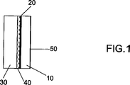
次いで、本発明のその他の特長及び利点を添付の図面を参照して説明する。なお、これらの図面において、図1は、電磁遮蔽フィルタの第1の実施形態を例示し、図2は、電磁遮蔽フィルタの第2の実施形態を例示し、そして図3は、本発明の多重層を概略的に例示している。 Other features and advantages of the present invention will now be described with reference to the accompanying drawings. In these drawings, FIG. 1 illustrates a first embodiment of the electromagnetic shielding filter, FIG. 2 illustrates a second embodiment of the electromagnetic shielding filter, and FIG. The multilayer is schematically illustrated.
本発明の要素のさまざまな寸法、特に厚みに関しては、図面中読取りをより容易にするように、一定の縮尺に基づいて描かれてはいないということをまず最初に指摘しておかなければならない。 It must first be pointed out that the various dimensions, in particular the thickness, of the elements according to the invention are not drawn to scale so that they are easier to read in the drawing.
図1は、光学及び電磁遮蔽フィルタを形成するためにプラズマディスプレイの前面に接合されるように意図された透明な構造体の1実施形態の第1の例を示している。 FIG. 1 shows a first example of one embodiment of a transparent structure intended to be joined to the front surface of a plasma display to form optical and electromagnetic shielding filters.
図示の構造体は、ディスプレイと同じ側に設置されるように意図された、ガラスタイプの、ただし一変形形態としてはプラスチックで作ることのできる第1の透明基板10、該構造体の内側に面して基板10の内部面の上に設置される本発明に従った薄膜多重層20、例えばPVBフィルムのようなプラスチックフィルム40を用いて多重層20に面して第1の基板に接合されるガラスタイプの第2の基板30を含んで成る。この機能的プラスチックフィルムは、有利には、590nmを中心とする波長のオレンジ色をろ光するべく有機染料又は鉱物顔料を包含し得る。該プラスチックフィルム又は該構造体の代替的実施形態についてのさらなる詳細に関しては、フランス特許出願第03/04636号明細書を参照することができる。
The illustrated structure is a first
構造体の外側に向かう基板10及び30の外部面には、好ましくは、反射防止コーティング50が備わっている。
The outer surface of the
図2は、見る人とは反対側にくるように意図された面の1つに薄膜多重層20が備わった基板10、及び第1の実施形態で上述した通りのその他の機能性を有利には包含しうる例えばPVBフィルムのようなプラスチックフィルム40を用いて多重層20に面して基板10に接合されている、ディスプレイと同じ側に設置されるように意図されている例えばPETのようなプラスチックで作られた基板60を含んで成る、構造体の実施形態の第2の例を示している。構造体の外側に向かう基板10の外部面には、好ましくは反射防止コーティング50が具備されている。
FIG. 2 advantageously illustrates the
従って、本発明は、例えば基板10のような基板上に被着された多重層20に関する。この多重層は、3つの金属銀層を包含し、Ag1は、基板に最も近い層であり、Ag2は中央層であり、Ag3は、30MHz〜1GHzの周波数をもつ電磁波及び800nmを超える赤外線波を反射することを機能とする最も遠く離れた銀層である。
Thus, the present invention relates to a multilayer 20 deposited on a substrate, such as
多重層は、基板上に交互に被着させられた状態で、二酸化チタン層21、酸化亜鉛層から成る金属酸化物層22、銀層Ag1、Ag2又はAg3の1つ及び犠牲金属の被覆層23を包含する。基板から最も遠くの銀層Ag3上に被着されている犠牲金属層23の上面に被着されているのは、少なくとも1つの金属酸化物から成る反射防止層24である。
Multilayers, in a state of being brought deposited alternately on the substrate, the
銀層Ag1、Ag2又はAg3の各々の厚みは、13nm〜19nmの間である。それぞれの層Ag1、Ag2及びAg3の厚みeAg1、eAg2及びeAg3は、同一であってよく、さもなければ、0.8〜1.2の間の比率で変動してもよく、eAg1≦eAg3≦eAg2となるようなものである。層の厚みの不均衡は、同じ表面抵抗を維持しながら光反射率を低下させるため、優先的である。 The thickness of each of the silver layers Ag 1 , Ag 2 or Ag 3 is between 13 nm and 19 nm. The thicknesses eAg 1 , eAg 2 and eAg 3 of the respective layers Ag 1 , Ag 2 and Ag 3 may be the same or may vary at a ratio between 0.8 and 1.2. EAg 1 ≦ eAg 3 ≦ eAg 2 . The layer thickness imbalance is preferential because it reduces the light reflectivity while maintaining the same surface resistance.
基板に近い銀層Ag1のための副層としての酸化チタン層21は、10〜20nm、好ましくは10〜15nmの間の厚みを有する。
The
その他の2つの銀層Ag2及びAg3のための副層としての酸化チタン層21は、35〜55nm、好ましくは40〜50nmの間の厚みを有する。
The
酸化亜鉛層22は、好ましくは、15nmを上回る、例えば16又は18nmの厚みを有する。
The
犠牲金属層23は、ニオブ、チタン又はジルコニウム、好ましくはチタンからなるものであり、最大2nm、例えば1.5nmの厚みを有する。
The
犠牲金属層は、銀を酸化から保護し、かつその低効率を改善することを可能にする。チタンの存在は、光透過率を劣化させ得るものの、それはまさに充分適正な光透過率を維持しながらさらに一層低い表面抵抗を得ることができるようにする。フィルタの光学特性とその遮蔽特性の間に見い出すべき妥協点は、優れた光学特性をなおも維持しながら遮蔽を優先させることによって提供される。かくして、3つの銀層に基づく本発明の層構成によると、表面抵抗は、先行技術に従った場合の1.5に比べ0.8Ω/□まで低下し、これは「消費者」製品と呼ばれるものを扱う欧州規格EN55022のクラスAを満たすだけでなく、ホームシネマタイプの特殊な製品を扱うクラスBをも満たすものである。 The sacrificial metal layer makes it possible to protect the silver from oxidation and to improve its low efficiency. Although the presence of titanium can degrade the light transmission, it makes it possible to obtain even lower surface resistances while maintaining just the right light transmission. A compromise to be found between the optical properties of a filter and its shielding properties is provided by prioritizing shielding while still maintaining excellent optical properties. Thus, according to the layer structure of the present invention based on three silver layers, the surface resistance is reduced to 0.8 Ω / □ compared to 1.5 according to the prior art, which is called a “consumer” product In addition to meeting Class A of the European standard EN55022 that handles things, it also meets Class B that handles special products of the home cinema type.
基板から遠隔した銀層Ag3のための反射防止層24は、25〜50nmの間、好ましくは25〜35nmの間の厚みを有する。この層は、15〜35nm、好ましくは20〜30nmの間の厚みの二酸化チタンを少なくとも含む。
有利には、この反射防止層の二酸化チタンの上面に被着されるものとして、5〜15nm、好ましくは6〜10nmの間の小さい厚みのもう1つの金属酸化物がある。この金属酸化物は、例えば、酸化錫(SnO2)又は窒化珪素(Si3N4)であり、反射及び透過における色の純度を改善する一助となる。 Advantageously, there is another metal oxide with a small thickness between 5 and 15 nm, preferably between 6 and 10 nm, which is deposited on the top surface of the titanium dioxide of this antireflection layer. This metal oxide is, for example, tin oxide (SnO 2 ) or silicon nitride (Si 3 N 4 ), which helps to improve the color purity in reflection and transmission.
多重層の全ての層は、既知のスパッタリング技術により基板上に被着される。 All layers of the multilayer are deposited on the substrate by known sputtering techniques.
下記の表では、本発明の多重層20の5つの例(例1〜例5)を示す。表中に示されているのは、各層の厚み(nm単位)、そして基板10に接合された各々の多重層について、光透過率TLの値(%単位)、光反射率RL(%単位)、透過における純度Pe in T(%単位)、反射における純度Pe in R(%単位)、透過及び反射における主波長、それぞれλd in T及びλd in R(nm単位)及び表面抵抗R surf(Ω/□単位)である。
In the table below, five examples (Examples 1 to 5) of the
これらの5つの例は、1Ω/□未満の適切な遮蔽を達成することを可能にする。 These five examples make it possible to achieve adequate shielding of less than 1 Ω / □.
例1、例2及び例5の場合、銀層は同じであり15nmに等しく、酸化亜鉛の厚みは異なり厚みは15nm未満であり、例5の場合は正確に10nmに等しい。各例について、二酸化チタン層の厚みは、多重層の光学特性を最適化するように固定される。 In Examples 1, 2 and 5, the silver layers are the same and equal to 15 nm, the thickness of the zinc oxide is different and the thickness is less than 15 nm, and in Example 5, it is exactly equal to 10 nm. For each example, the thickness of the titanium dioxide layer is fixed to optimize the optical properties of the multilayer.
結果から、例5よりも大きい酸化亜鉛の厚み(6〜8nm及びそれ以上)を有する例1及び例2について、光透過率が、先行技術に関して予想されうるものとは異なり、実質的に同一にとどまっているか又は例1の場合にはわずかに上回っていさえし、酸化亜鉛の厚みは18nmであり、又反射は、例1及び例2の場合、例5の場合に比べ低いものであるという利点を有し、かくして、見る人にとって眩しくない攻撃性の低い形でディスプレイを照射することを可能にしている、ということがわかる。 The results show that for Examples 1 and 2 having a zinc oxide thickness (6-8 nm and above) greater than Example 5, the light transmission is substantially the same, unlike what could be expected for the prior art. Advantages of staying or even slightly exceeding in the case of Example 1, the zinc oxide thickness being 18 nm and the reflection being lower in the case of Examples 1 and 2 than in Example 5. Thus, it can be seen that the display can be illuminated in a less aggressive form that is not dazzling for the viewer.
例3及び例4は、銀層に関して等しくない厚みで、例4の場合SnO2に基づく反射防止層25との比較を提供している。不均衡は、光反射率を低減させるという利点をもつが、透過及び反射における純度を増大させるという欠点を有する。反射防止層の付加は、この欠点を克服し、かくして例1、例2及び例5のものと同等の又は実質的に同等の透過における純度を得る一助となる。 Examples 3 and 4 provide a comparison with the anti-reflective layer 25 based on SnO 2 in the case of Example 4 with unequal thickness with respect to the silver layer. Imbalance has the advantage of reducing light reflectivity, but has the disadvantage of increasing purity in transmission and reflection. The addition of an anti-reflective layer helps to overcome this disadvantage and thus obtain a purity in transmission that is equivalent or substantially equivalent to that of Examples 1, 2 and 5.

かくして、銀及び誘電層の被着及び本発明に従って作成された厚みを制御すると同時に金属保護層を使用することによって、図1又は図2を参照して得られたフィルタは以下の特性を有する:
1Ω/□未満の表面抵抗;
45〜55%の間の光透過率TL;
10%未満の透過における純度;
5%未満、好ましくは4%未満の光反射率RL;
20%未満の純度での反射における主として紫−青の色;及び
透過における主として青の色。
Thus, by controlling the deposition of silver and dielectric layers and the thickness produced according to the present invention while simultaneously using a metal protective layer, the filter obtained with reference to FIG. 1 or 2 has the following characteristics:
Surface resistance of less than 1Ω / □;
Light transmittance T L between 45-55%;
Purity at a transmission of less than 10%;
A light reflectivity R L of less than 5%, preferably less than 4%;
A predominantly purple-blue color in reflection with a purity of less than 20%; and a predominantly blue color in transmission.
本発明の基板を用いた電磁遮蔽フィルタは、表示スクリーン、特にプラズマディスプレイに応用することができる。それは、遮蔽に関し非常に優れた性能を提供し(表面抵抗は1Ω/□未満)、その結果、900nmでの透過率が1%を超えず、特に赤外線を遮断する。このフィルタは同様に、優れた視認性(光透過率は45〜55%の間)を提供し、ディスプレイのコントラストを改善する。 The electromagnetic shielding filter using the substrate of the present invention can be applied to a display screen, particularly a plasma display. It provides very good performance with respect to shielding (surface resistance is less than 1 Ω / □), so that the transmission at 900 nm does not exceed 1% and in particular blocks infrared radiation. This filter also provides excellent visibility (light transmission between 45-55%) and improves display contrast.
Claims (13)
金属酸化物が酸化亜鉛であること;
被覆層(23)が犠牲金属であること;
少なくとも1つの金属酸化物を含む反射防止層(24)が、基板から最も遠く離れた銀層(Ag3)のための被覆層(23)上に被着されていること;
銀層(Ag 1 ,Ag 2 ,Ag 3 )の各々の厚みが13nm〜19nmの間であること;及び
犠牲金属からなる被覆層(23)が、2nmを超えない厚みを有すること、
を特徴とする透明基板。Including three silver layers (Ag 1 , Ag 2 , Ag 3 ) and one of a titanium dioxide layer (21), a metal oxide layer (22), a silver layer (Ag 1 , Ag 2 , Ag 3 ) and In a transparent substrate with thin film multilayers (20) comprising alternating coating layers (23) on the substrate,
The metal oxide is zinc oxide;
The covering layer (23) is a sacrificial metal ;
An antireflective layer (24) comprising at least one metal oxide is deposited on the covering layer (23) for the silver layer (Ag 3 ) furthest away from the substrate ;
The thickness of each of the silver layers (Ag 1 , Ag 2 , Ag 3 ) is between 13 nm and 19 nm; and
The covering layer (23) made of the sacrificial metal has a thickness not exceeding 2 nm ,
A transparent substrate characterized by.
45〜55%の間の光透過率TL;
透過における10%未満の純度;
5%未満の光反射率RL;
20%未満の純度での反射における主として紫−青の色;
透過における主として青の色、
を有することを特徴とする請求項1〜11のいずれか1項に記載の基板を含む電磁遮蔽フィルタ。Optical properties such as:
Light transmittance T L between 45-55%;
A purity of less than 10% in permeation;
A light reflectance R L of less than 5%;
Predominantly purple-blue color in reflections with a purity of less than 20%;
Mainly blue color in transmission,
Electromagnetic shielding filter comprising a substrate according to any one of claims 1 to 11, characterized in that it comprises a.
Applications Claiming Priority (3)
| Application Number | Priority Date | Filing Date | Title |
|---|---|---|---|
| FR0310912A FR2859721B1 (en) | 2003-09-17 | 2003-09-17 | TRANSPARENT SUBSTRATE WITH THIN FILM STACK FOR ELECTROMAGNETIC SHIELDING |
| FR0310912 | 2003-09-17 | ||
| PCT/FR2004/002152 WO2005028391A1 (en) | 2003-09-17 | 2004-08-18 | Transparent substrate comprising a stack of thin layers for electromagnetic armour |
Publications (3)
| Publication Number | Publication Date |
|---|---|
| JP2007505810A JP2007505810A (en) | 2007-03-15 |
| JP2007505810A5 JP2007505810A5 (en) | 2007-08-16 |
| JP4800947B2 true JP4800947B2 (en) | 2011-10-26 |
Family
ID=34203512
Family Applications (1)
| Application Number | Title | Priority Date | Filing Date |
|---|---|---|---|
| JP2006526656A Expired - Fee Related JP4800947B2 (en) | 2003-09-17 | 2004-08-18 | Transparent substrate with thin film laminate for electromagnetic shielding |
Country Status (11)
| Country | Link |
|---|---|
| US (2) | US7452603B2 (en) |
| EP (1) | EP1663897B1 (en) |
| JP (1) | JP4800947B2 (en) |
| KR (1) | KR101148039B1 (en) |
| CN (1) | CN1852871B (en) |
| AT (1) | ATE441624T1 (en) |
| DE (1) | DE602004022955D1 (en) |
| FR (1) | FR2859721B1 (en) |
| MX (1) | MXPA06002831A (en) |
| PL (1) | PL1663897T3 (en) |
| WO (1) | WO2005028391A1 (en) |
Families Citing this family (54)
| Publication number | Priority date | Publication date | Assignee | Title |
|---|---|---|---|---|
| FR2862961B1 (en) | 2003-11-28 | 2006-02-17 | Saint Gobain | TRANSPARENT SUBSTRATE USED ALTERNATELY OR CUMULATIVELY FOR THERMAL CONTROL, ELECTROMAGNETIC SHIELDING AND HEATED GLAZING. |
| JP2006327177A (en) * | 2005-04-26 | 2006-12-07 | Tokai Rubber Ind Ltd | Transparent laminated film, transparent laminate and plasma display |
| FR2889182B1 (en) * | 2005-07-29 | 2007-10-26 | Saint Gobain | GLAZING PROVIDED WITH A STACK OF THIN LAYERS ACTING ON SOLAR RADIATION |
| US7342716B2 (en) * | 2005-10-11 | 2008-03-11 | Cardinal Cg Company | Multiple cavity low-emissivity coatings |
| US7339728B2 (en) | 2005-10-11 | 2008-03-04 | Cardinal Cg Company | Low-emissivity coatings having high visible transmission and low solar heat gain coefficient |
| US7572511B2 (en) * | 2005-10-11 | 2009-08-11 | Cardinal Cg Company | High infrared reflection coatings |
| FR2892409B1 (en) * | 2005-10-25 | 2007-12-14 | Saint Gobain | PROCESS FOR TREATING A SUBSTRATE |
| KR100926233B1 (en) * | 2006-05-30 | 2009-11-09 | 삼성코닝정밀유리 주식회사 | Pdp filter having multi-layer thin film and method for manufacturing the same |
| JP4935215B2 (en) * | 2006-07-18 | 2012-05-23 | 日亜化学工業株式会社 | Light emitting device |
| JP4982149B2 (en) * | 2006-10-25 | 2012-07-25 | 東海ゴム工業株式会社 | Transparent laminated film and transparent laminated body |
| WO2008065962A1 (en) * | 2006-11-27 | 2008-06-05 | National Institute Of Advanced Industrial Science And Technology | Visible light transparent and heat reflective sheet |
| FR2911130B1 (en) * | 2007-01-05 | 2009-11-27 | Saint Gobain | THIN FILM DEPOSITION METHOD AND PRODUCT OBTAINED |
| US8025957B2 (en) | 2007-05-09 | 2011-09-27 | Ppg Industries Ohio, Inc. | Vehicle transparency |
| EP2183102B1 (en) * | 2007-08-24 | 2018-03-14 | Vitro, S.A.B. de C.V. | Vehicle transparency |
| US8658289B2 (en) | 2007-11-16 | 2014-02-25 | Ppg Industries Ohio, Inc. | Electromagnetic radiation shielding device |
| DE102007061419A1 (en) * | 2007-12-20 | 2009-06-25 | Fraunhofer-Gesellschaft zur Förderung der angewandten Forschung e.V. | Transparent plastic film for shielding electromagnetic waves and method for producing such a plastic film |
| US7713633B2 (en) * | 2008-05-27 | 2010-05-11 | Guardian Industries Corp. | EMI filter for plasma display panel |
| US8592059B2 (en) | 2008-08-21 | 2013-11-26 | Guardian Industries Corp. | Plasma display panel including EMI filter, and/or method of making the same |
| FR2936510B1 (en) * | 2008-09-30 | 2019-08-30 | Saint-Gobain Glass France | SUBSTRATE PROVIDED WITH A STACK WITH THERMAL PROPERTIES, ESPECIALLY FOR REALIZING A HEATED GLAZING. |
| KR101056438B1 (en) * | 2008-12-05 | 2011-08-11 | 삼성에스디아이 주식회사 | Display panel and optical filter |
| US10654748B2 (en) | 2010-03-29 | 2020-05-19 | Vitro Flat Glass Llc | Solar control coatings providing increased absorption or tint |
| US10654747B2 (en) | 2010-03-29 | 2020-05-19 | Vitro Flat Glass Llc | Solar control coatings with subcritical copper |
| US8865325B2 (en) * | 2010-03-29 | 2014-10-21 | Ppg Industries Ohio, Inc. | Tempered and non-tempered glass coatings having similar optical characteristics |
| US9932267B2 (en) | 2010-03-29 | 2018-04-03 | Vitro, S.A.B. De C.V. | Solar control coatings with discontinuous metal layer |
| FR2970248B1 (en) | 2011-01-06 | 2019-08-30 | Saint-Gobain Glass France | SUBSTRATE PROVIDED WITH A STACK WITH THERMAL PROPERTIES, ESPECIALLY FOR REALIZING A HEATED GLAZING. |
| GB201106788D0 (en) * | 2011-04-21 | 2011-06-01 | Pilkington Group Ltd | Heat treatable coated glass pane |
| PL2803245T3 (en) | 2012-01-10 | 2017-08-31 | Saint-Gobain Glass France | Transparent pane with electrically heatable coating |
| WO2013104438A1 (en) | 2012-01-10 | 2013-07-18 | Saint-Gobain Glass France | Transparent panel with electrically conductive coating |
| FR2985724B1 (en) * | 2012-01-16 | 2014-03-07 | Saint Gobain | SUBSTRATE PROVIDED WITH A STACK WITH THERMAL PROPERTIES COMPRISING FOUR METAL FUNCTIONAL LAYERS. |
| WO2013109582A1 (en) * | 2012-01-17 | 2013-07-25 | Cardinal Cg Company | Low solar transmittance coatings |
| US9279910B2 (en) * | 2013-03-13 | 2016-03-08 | Intermolecular, Inc. | Color shift of high LSG low emissivity coating after heat treatment |
| US9790127B2 (en) * | 2013-03-14 | 2017-10-17 | Intermolecular, Inc. | Method to generate high LSG low-emissivity coating with same color after heat treatment |
| FR3005048B1 (en) * | 2013-04-30 | 2020-09-25 | Saint Gobain | SUBSTRATE EQUIPPED WITH A STACKING WITH THERMAL PROPERTIES |
| CN103264549B (en) * | 2013-05-17 | 2017-10-10 | 中国南玻集团股份有限公司 | The front infrared shield glass consistent with offside reflection tone |
| US8940400B1 (en) | 2013-09-03 | 2015-01-27 | Guardian Industries Corp. | IG window unit including double silver coating having increased SHGC to U-value ratio, and corresponding coated article for use in IG window unit or other window |
| CN104609740B (en) * | 2015-02-04 | 2018-04-10 | 中国建筑材料科学研究总院 | Can monolithic using sunlight controlling coated glass and preparation method thereof |
| EP3310728B1 (en) * | 2015-06-19 | 2021-06-02 | AGC Glass Europe | Laminated glazing for solar control |
| FR3038597B1 (en) * | 2015-07-08 | 2021-12-10 | Saint Gobain | MATERIAL EQUIPPED WITH A THERMAL PROPERTIES STACK |
| US10942302B2 (en) * | 2015-09-16 | 2021-03-09 | Vitro Flat Glass Llc | Solar mirrors and methods of making solar mirrors having improved properties |
| US10528748B2 (en) * | 2016-04-22 | 2020-01-07 | International Business Machines Corporation | Context-driven on-device data protection |
| FR3051804B1 (en) * | 2016-05-24 | 2018-06-29 | Saint-Gobain Glass France | THIN LAYER DEPOSITION METHOD |
| CN106435475B (en) * | 2016-09-08 | 2018-09-14 | 江苏双星彩塑新材料股份有限公司 | A kind of energy saving fenestrated membrane of blue-green three-silver low radiation and preparation method thereof |
| CN106637108B (en) * | 2016-09-08 | 2019-01-25 | 江苏双星彩塑新材料股份有限公司 | High heat-insulating and energy-saving fenestrated membranes of a kind of indigo pair silver and preparation method thereof |
| CN109716180B (en) * | 2016-09-15 | 2021-03-09 | 中央硝子株式会社 | Solar radiation shielding member |
| FR3056580B1 (en) * | 2016-09-26 | 2021-02-12 | Saint Gobain | SUBSTRATE COATED WITH A LOW-EMISSIVE COATING |
| FR3056579B1 (en) * | 2016-09-26 | 2021-02-12 | Saint Gobain | SUBSTRATE COATED WITH A LOW-EMISSIVE COATING |
| US10556823B2 (en) | 2017-06-20 | 2020-02-11 | Apple Inc. | Interior coatings for glass structures in electronic devices |
| FR3069241B1 (en) * | 2017-07-21 | 2022-02-04 | Saint Gobain | MATERIAL COMPRISING A STACK WITH THERMAL PROPERTIES |
| US11078718B2 (en) | 2018-02-05 | 2021-08-03 | Vitro Flat Glass Llc | Solar control coatings with quadruple metallic layers |
| FR3082198B1 (en) * | 2018-06-12 | 2020-06-26 | Saint-Gobain Glass France | MATERIAL COMPRISING A STACK WITH THERMAL AND AESTHETIC PROPERTIES |
| FR3082199B1 (en) * | 2018-06-12 | 2020-06-26 | Saint-Gobain Glass France | MATERIAL COMPRISING A STACK WITH THERMAL AND AESTHETIC PROPERTIES |
| JP6748150B2 (en) * | 2018-06-14 | 2020-08-26 | ファナック株式会社 | Galvano mirror and laser processing equipment |
| CN112888288B (en) * | 2021-01-18 | 2022-10-28 | 哈尔滨工业大学 | Electromagnetic shielding curved surface optical window based on ultrathin doped metal/medium composite structure |
| CN114719683A (en) * | 2022-04-01 | 2022-07-08 | 江苏铁锚玻璃股份有限公司 | Silver-based electromagnetic shielding and electromagnetic stealth film system structure |
Citations (7)
| Publication number | Priority date | Publication date | Assignee | Title |
|---|---|---|---|---|
| JPH02289449A (en) * | 1989-01-05 | 1990-11-29 | Glaverbel Sa | Coated glass material and its method |
| JPH07108642A (en) * | 1993-08-20 | 1995-04-25 | Asahi Glass Co Ltd | Functional article |
| JP2000252682A (en) * | 1999-02-26 | 2000-09-14 | Central Glass Co Ltd | Substrate with electromagnetic shielding film |
| JP2001146438A (en) * | 1999-11-16 | 2001-05-29 | Asahi Breweries Ltd | Method for treating outer surface of glass bottle and the resultant glass bottle |
| JP2002072897A (en) * | 2000-08-25 | 2002-03-12 | Fuji Photo Film Co Ltd | Electromagnetic wave shieldable transparent film |
| US20030049464A1 (en) * | 2001-09-04 | 2003-03-13 | Afg Industries, Inc. | Double silver low-emissivity and solar control coatings |
| JP2003133787A (en) * | 2001-10-26 | 2003-05-09 | Central Glass Co Ltd | Substrate with electromagnetic wave shielding film |
Family Cites Families (6)
| Publication number | Priority date | Publication date | Assignee | Title |
|---|---|---|---|---|
| CA1331867C (en) * | 1986-12-29 | 1994-09-06 | James Joseph Finley | Low emissivity film for high temperature processing |
| FR2755962B1 (en) * | 1996-11-21 | 1998-12-24 | Saint Gobain Vitrage | GLAZING COMPRISING A SUBSTRATE PROVIDED WITH A STACK OF THIN FILMS FOR SUN PROTECTION AND / OR THERMAL INSULATION |
| DE19726966C1 (en) * | 1997-06-25 | 1999-01-28 | Flachglas Ag | Process for the production of a transparent silver layer with a high specific electrical conductivity, glass pane with a thin layer system with such a silver layer and its use |
| JPH11307987A (en) * | 1998-04-16 | 1999-11-05 | Nippon Sheet Glass Co Ltd | Electromagnetic wave filter |
| KR100424254B1 (en) * | 1999-08-06 | 2004-03-22 | 삼성에스디아이 주식회사 | Optical filter for plasma display device |
| CA2475192C (en) * | 2002-02-11 | 2008-12-09 | Ppg Industries Ohio, Inc. | Solar control coating |
-
2003
- 2003-09-17 FR FR0310912A patent/FR2859721B1/en not_active Expired - Fee Related
-
2004
- 2004-08-18 WO PCT/FR2004/002152 patent/WO2005028391A1/en active Application Filing
- 2004-08-18 AT AT04786318T patent/ATE441624T1/en not_active IP Right Cessation
- 2004-08-18 MX MXPA06002831A patent/MXPA06002831A/en active IP Right Grant
- 2004-08-18 CN CN2004800267040A patent/CN1852871B/en not_active Expired - Fee Related
- 2004-08-18 PL PL04786318T patent/PL1663897T3/en unknown
- 2004-08-18 KR KR1020067004999A patent/KR101148039B1/en active IP Right Grant
- 2004-08-18 DE DE602004022955T patent/DE602004022955D1/en active Active
- 2004-08-18 EP EP04786318A patent/EP1663897B1/en active Active
- 2004-08-18 US US10/572,286 patent/US7452603B2/en not_active Expired - Fee Related
- 2004-08-18 JP JP2006526656A patent/JP4800947B2/en not_active Expired - Fee Related
-
2008
- 2008-09-22 US US12/234,881 patent/US20090015909A1/en not_active Abandoned
Patent Citations (7)
| Publication number | Priority date | Publication date | Assignee | Title |
|---|---|---|---|---|
| JPH02289449A (en) * | 1989-01-05 | 1990-11-29 | Glaverbel Sa | Coated glass material and its method |
| JPH07108642A (en) * | 1993-08-20 | 1995-04-25 | Asahi Glass Co Ltd | Functional article |
| JP2000252682A (en) * | 1999-02-26 | 2000-09-14 | Central Glass Co Ltd | Substrate with electromagnetic shielding film |
| JP2001146438A (en) * | 1999-11-16 | 2001-05-29 | Asahi Breweries Ltd | Method for treating outer surface of glass bottle and the resultant glass bottle |
| JP2002072897A (en) * | 2000-08-25 | 2002-03-12 | Fuji Photo Film Co Ltd | Electromagnetic wave shieldable transparent film |
| US20030049464A1 (en) * | 2001-09-04 | 2003-03-13 | Afg Industries, Inc. | Double silver low-emissivity and solar control coatings |
| JP2003133787A (en) * | 2001-10-26 | 2003-05-09 | Central Glass Co Ltd | Substrate with electromagnetic wave shielding film |
Also Published As
| Publication number | Publication date |
|---|---|
| KR101148039B1 (en) | 2012-07-05 |
| EP1663897B1 (en) | 2009-09-02 |
| CN1852871A (en) | 2006-10-25 |
| US20090015909A1 (en) | 2009-01-15 |
| JP2007505810A (en) | 2007-03-15 |
| WO2005028391A1 (en) | 2005-03-31 |
| MXPA06002831A (en) | 2006-06-14 |
| US7452603B2 (en) | 2008-11-18 |
| FR2859721A1 (en) | 2005-03-18 |
| DE602004022955D1 (en) | 2009-10-15 |
| KR20060073955A (en) | 2006-06-29 |
| EP1663897A1 (en) | 2006-06-07 |
| US20060280951A1 (en) | 2006-12-14 |
| ATE441624T1 (en) | 2009-09-15 |
| FR2859721B1 (en) | 2006-08-25 |
| CN1852871B (en) | 2011-10-05 |
| PL1663897T3 (en) | 2010-02-26 |
Similar Documents
| Publication | Publication Date | Title |
|---|---|---|
| JP4800947B2 (en) | Transparent substrate with thin film laminate for electromagnetic shielding | |
| JP4666087B2 (en) | Protection plate for plasma display | |
| KR101395681B1 (en) | Antireflecttion-coated transparent substrate exhibiting neutral colour in reflection | |
| US20050074591A1 (en) | Transparent substrate with antiglare coating having abrasion-resistant properties | |
| JP5399893B2 (en) | Handling of zinc-based thin films for optical filters | |
| JP2003500249A (en) | Transparent substrate with anti-reflective, low emissivity or sun protection coating | |
| WO2006033861A2 (en) | Plasma display filter with a dielectric/metallic layer stack of at least eleven layers | |
| JP2003500249A5 (en) | ||
| WO2009145864A1 (en) | Emi filter for plasma display panel | |
| JP5098137B2 (en) | Antireflection film | |
| JP4355327B2 (en) | Protection plate for plasma display | |
| JP2006313918A5 (en) | ||
| KR100840688B1 (en) | Multi-layer thin film structure of pdp filter | |
| KR100618374B1 (en) | Pdp filter having structure of multi-layer thin film | |
| KR100715443B1 (en) | Multi-layer thin film structure of pdp filter | |
| JP2006243757A (en) | Protective plate for plasma display and manufacturing method thereof | |
| JP2006133799A (en) | Protective plate for plasma display and manufacturing method thereof | |
| KR20030093734A (en) | Multi-layer thin film structure of pdp filter | |
| JP4086905B2 (en) | Protection plate for plasma display and manufacturing method thereof | |
| JP2004264350A (en) | Front filter | |
| JP2006163428A (en) | Protective plate for plasma display and method for producing the same |
Legal Events
| Date | Code | Title | Description |
|---|---|---|---|
| A521 | Request for written amendment filed |
Free format text: JAPANESE INTERMEDIATE CODE: A523 Effective date: 20070614 |
|
| A621 | Written request for application examination |
Free format text: JAPANESE INTERMEDIATE CODE: A621 Effective date: 20070614 |
|
| A131 | Notification of reasons for refusal |
Free format text: JAPANESE INTERMEDIATE CODE: A131 Effective date: 20100803 |
|
| A601 | Written request for extension of time |
Free format text: JAPANESE INTERMEDIATE CODE: A601 Effective date: 20101102 |
|
| A602 | Written permission of extension of time |
Free format text: JAPANESE INTERMEDIATE CODE: A602 Effective date: 20101110 |
|
| A521 | Request for written amendment filed |
Free format text: JAPANESE INTERMEDIATE CODE: A523 Effective date: 20110202 |
|
| TRDD | Decision of grant or rejection written | ||
| A01 | Written decision to grant a patent or to grant a registration (utility model) |
Free format text: JAPANESE INTERMEDIATE CODE: A01 Effective date: 20110705 |
|
| A01 | Written decision to grant a patent or to grant a registration (utility model) |
Free format text: JAPANESE INTERMEDIATE CODE: A01 |
|
| A61 | First payment of annual fees (during grant procedure) |
Free format text: JAPANESE INTERMEDIATE CODE: A61 Effective date: 20110804 |
|
| FPAY | Renewal fee payment (event date is renewal date of database) |
Free format text: PAYMENT UNTIL: 20140812 Year of fee payment: 3 |
|
| R150 | Certificate of patent or registration of utility model |
Ref document number: 4800947 Country of ref document: JP Free format text: JAPANESE INTERMEDIATE CODE: R150 Free format text: JAPANESE INTERMEDIATE CODE: R150 |
|
| R250 | Receipt of annual fees |
Free format text: JAPANESE INTERMEDIATE CODE: R250 |
|
| R250 | Receipt of annual fees |
Free format text: JAPANESE INTERMEDIATE CODE: R250 |
|
| R250 | Receipt of annual fees |
Free format text: JAPANESE INTERMEDIATE CODE: R250 |
|
| R250 | Receipt of annual fees |
Free format text: JAPANESE INTERMEDIATE CODE: R250 |
|
| R250 | Receipt of annual fees |
Free format text: JAPANESE INTERMEDIATE CODE: R250 |
|
| R250 | Receipt of annual fees |
Free format text: JAPANESE INTERMEDIATE CODE: R250 |
|
| LAPS | Cancellation because of no payment of annual fees |