JP4797185B2 - Bipolar junction transistor compatible with vertical replacement gate transistor - Google Patents
Bipolar junction transistor compatible with vertical replacement gate transistor Download PDFInfo
- Publication number
- JP4797185B2 JP4797185B2 JP2002270858A JP2002270858A JP4797185B2 JP 4797185 B2 JP4797185 B2 JP 4797185B2 JP 2002270858 A JP2002270858 A JP 2002270858A JP 2002270858 A JP2002270858 A JP 2002270858A JP 4797185 B2 JP4797185 B2 JP 4797185B2
- Authority
- JP
- Japan
- Prior art keywords
- doped
- region
- insulating layer
- forming
- layer
- Prior art date
- Legal status (The legal status is an assumption and is not a legal conclusion. Google has not performed a legal analysis and makes no representation as to the accuracy of the status listed.)
- Expired - Fee Related
Links
- 239000004065 semiconductor Substances 0.000 claims description 103
- 238000000034 method Methods 0.000 claims description 85
- 239000000463 material Substances 0.000 claims description 73
- 239000002019 doping agent Substances 0.000 claims description 43
- VYPSYNLAJGMNEJ-UHFFFAOYSA-N Silicium dioxide Chemical compound O=[Si]=O VYPSYNLAJGMNEJ-UHFFFAOYSA-N 0.000 claims description 42
- 238000012545 processing Methods 0.000 claims description 40
- 230000008569 process Effects 0.000 claims description 36
- 239000000758 substrate Substances 0.000 claims description 32
- 235000012239 silicon dioxide Nutrition 0.000 claims description 19
- 239000000377 silicon dioxide Substances 0.000 claims description 19
- XUIMIQQOPSSXEZ-UHFFFAOYSA-N Silicon Chemical compound [Si] XUIMIQQOPSSXEZ-UHFFFAOYSA-N 0.000 claims description 17
- 229910052710 silicon Inorganic materials 0.000 claims description 17
- 239000010703 silicon Substances 0.000 claims description 17
- 238000005530 etching Methods 0.000 claims description 14
- 238000009792 diffusion process Methods 0.000 claims description 13
- 229910052581 Si3N4 Inorganic materials 0.000 claims description 11
- HQVNEWCFYHHQES-UHFFFAOYSA-N silicon nitride Chemical compound N12[Si]34N5[Si]62N3[Si]51N64 HQVNEWCFYHHQES-UHFFFAOYSA-N 0.000 claims description 11
- 238000005229 chemical vapour deposition Methods 0.000 claims description 9
- QVGXLLKOCUKJST-UHFFFAOYSA-N atomic oxygen Chemical compound [O] QVGXLLKOCUKJST-UHFFFAOYSA-N 0.000 claims description 6
- 229910052760 oxygen Inorganic materials 0.000 claims description 6
- 239000001301 oxygen Substances 0.000 claims description 6
- 238000010438 heat treatment Methods 0.000 claims description 5
- 238000002513 implantation Methods 0.000 claims description 5
- 238000011065 in-situ storage Methods 0.000 claims description 5
- 229910044991 metal oxide Inorganic materials 0.000 claims description 5
- 150000004706 metal oxides Chemical class 0.000 claims description 5
- 229910000577 Silicon-germanium Inorganic materials 0.000 claims description 4
- AXQKVSDUCKWEKE-UHFFFAOYSA-N [C].[Ge].[Si] Chemical compound [C].[Ge].[Si] AXQKVSDUCKWEKE-UHFFFAOYSA-N 0.000 claims description 4
- LEVVHYCKPQWKOP-UHFFFAOYSA-N [Si].[Ge] Chemical compound [Si].[Ge] LEVVHYCKPQWKOP-UHFFFAOYSA-N 0.000 claims description 4
- 238000000231 atomic layer deposition Methods 0.000 claims description 3
- 239000004020 conductor Substances 0.000 claims description 3
- 239000003989 dielectric material Substances 0.000 claims description 3
- 238000001312 dry etching Methods 0.000 claims description 3
- 238000001039 wet etching Methods 0.000 claims description 3
- 230000008020 evaporation Effects 0.000 claims 2
- 238000001704 evaporation Methods 0.000 claims 2
- 238000003672 processing method Methods 0.000 claims 1
- 239000007787 solid Substances 0.000 claims 1
- 230000015572 biosynthetic process Effects 0.000 description 10
- 239000007790 solid phase Substances 0.000 description 10
- KRHYYFGTRYWZRS-UHFFFAOYSA-N Fluorane Chemical compound F KRHYYFGTRYWZRS-UHFFFAOYSA-N 0.000 description 6
- 238000004519 manufacturing process Methods 0.000 description 5
- 238000000151 deposition Methods 0.000 description 4
- 238000013461 design Methods 0.000 description 4
- 230000005669 field effect Effects 0.000 description 4
- 229910052814 silicon oxide Inorganic materials 0.000 description 4
- ZOXJGFHDIHLPTG-UHFFFAOYSA-N Boron Chemical compound [B] ZOXJGFHDIHLPTG-UHFFFAOYSA-N 0.000 description 3
- CBENFWSGALASAD-UHFFFAOYSA-N Ozone Chemical compound [O-][O+]=O CBENFWSGALASAD-UHFFFAOYSA-N 0.000 description 3
- 229910021417 amorphous silicon Inorganic materials 0.000 description 3
- 229910052796 boron Inorganic materials 0.000 description 3
- 230000008021 deposition Effects 0.000 description 3
- 238000009826 distribution Methods 0.000 description 3
- 238000001459 lithography Methods 0.000 description 3
- 229910052751 metal Inorganic materials 0.000 description 3
- 239000002184 metal Substances 0.000 description 3
- 229910021420 polycrystalline silicon Inorganic materials 0.000 description 3
- OAICVXFJPJFONN-UHFFFAOYSA-N Phosphorus Chemical group [P] OAICVXFJPJFONN-UHFFFAOYSA-N 0.000 description 2
- 230000009471 action Effects 0.000 description 2
- 238000000137 annealing Methods 0.000 description 2
- 230000004888 barrier function Effects 0.000 description 2
- 230000008901 benefit Effects 0.000 description 2
- 230000008859 change Effects 0.000 description 2
- 238000004140 cleaning Methods 0.000 description 2
- 150000001875 compounds Chemical class 0.000 description 2
- 239000011521 glass Substances 0.000 description 2
- BHEPBYXIRTUNPN-UHFFFAOYSA-N hydridophosphorus(.) (triplet) Chemical compound [PH] BHEPBYXIRTUNPN-UHFFFAOYSA-N 0.000 description 2
- 238000009413 insulation Methods 0.000 description 2
- 238000005468 ion implantation Methods 0.000 description 2
- 150000002739 metals Chemical class 0.000 description 2
- 229910052698 phosphorus Inorganic materials 0.000 description 2
- 239000011574 phosphorus Substances 0.000 description 2
- 238000000623 plasma-assisted chemical vapour deposition Methods 0.000 description 2
- 125000006850 spacer group Chemical group 0.000 description 2
- 239000000126 substance Substances 0.000 description 2
- 241000252506 Characiformes Species 0.000 description 1
- ZOKXTWBITQBERF-UHFFFAOYSA-N Molybdenum Chemical compound [Mo] ZOKXTWBITQBERF-UHFFFAOYSA-N 0.000 description 1
- BOTDANWDWHJENH-UHFFFAOYSA-N Tetraethyl orthosilicate Chemical compound CCO[Si](OCC)(OCC)OCC BOTDANWDWHJENH-UHFFFAOYSA-N 0.000 description 1
- RTAQQCXQSZGOHL-UHFFFAOYSA-N Titanium Chemical compound [Ti] RTAQQCXQSZGOHL-UHFFFAOYSA-N 0.000 description 1
- NRTOMJZYCJJWKI-UHFFFAOYSA-N Titanium nitride Chemical compound [Ti]#N NRTOMJZYCJJWKI-UHFFFAOYSA-N 0.000 description 1
- SCMCGJZNZWBQDK-UHFFFAOYSA-N [Si](O)(O)(O)O.C=C.C=C.C=C.C=C Chemical compound [Si](O)(O)(O)O.C=C.C=C.C=C.C=C SCMCGJZNZWBQDK-UHFFFAOYSA-N 0.000 description 1
- 238000009825 accumulation Methods 0.000 description 1
- 230000002411 adverse Effects 0.000 description 1
- 229910052787 antimony Inorganic materials 0.000 description 1
- WATWJIUSRGPENY-UHFFFAOYSA-N antimony atom Chemical compound [Sb] WATWJIUSRGPENY-UHFFFAOYSA-N 0.000 description 1
- 229910052785 arsenic Inorganic materials 0.000 description 1
- RQNWIZPPADIBDY-UHFFFAOYSA-N arsenic atom Chemical compound [As] RQNWIZPPADIBDY-UHFFFAOYSA-N 0.000 description 1
- 239000003990 capacitor Substances 0.000 description 1
- 230000015556 catabolic process Effects 0.000 description 1
- 239000002800 charge carrier Substances 0.000 description 1
- 238000006243 chemical reaction Methods 0.000 description 1
- 239000013078 crystal Substances 0.000 description 1
- 230000007423 decrease Effects 0.000 description 1
- 230000007547 defect Effects 0.000 description 1
- 230000002950 deficient Effects 0.000 description 1
- 238000005137 deposition process Methods 0.000 description 1
- 239000007772 electrode material Substances 0.000 description 1
- 238000009713 electroplating Methods 0.000 description 1
- 238000001912 gas jet deposition Methods 0.000 description 1
- 230000009931 harmful effect Effects 0.000 description 1
- 238000007373 indentation Methods 0.000 description 1
- 239000011810 insulating material Substances 0.000 description 1
- 239000012212 insulator Substances 0.000 description 1
- 150000002500 ions Chemical class 0.000 description 1
- 238000002955 isolation Methods 0.000 description 1
- 239000007788 liquid Substances 0.000 description 1
- 238000003754 machining Methods 0.000 description 1
- 229910052750 molybdenum Inorganic materials 0.000 description 1
- 239000011733 molybdenum Substances 0.000 description 1
- 229910021421 monocrystalline silicon Inorganic materials 0.000 description 1
- 150000004767 nitrides Chemical class 0.000 description 1
- 230000003647 oxidation Effects 0.000 description 1
- 238000007254 oxidation reaction Methods 0.000 description 1
- 238000004806 packaging method and process Methods 0.000 description 1
- 238000012856 packing Methods 0.000 description 1
- 230000000149 penetrating effect Effects 0.000 description 1
- 230000035515 penetration Effects 0.000 description 1
- 238000001020 plasma etching Methods 0.000 description 1
- 238000005498 polishing Methods 0.000 description 1
- 239000002243 precursor Substances 0.000 description 1
- 230000005855 radiation Effects 0.000 description 1
- 230000009467 reduction Effects 0.000 description 1
- 229910052715 tantalum Inorganic materials 0.000 description 1
- GUVRBAGPIYLISA-UHFFFAOYSA-N tantalum atom Chemical compound [Ta] GUVRBAGPIYLISA-UHFFFAOYSA-N 0.000 description 1
- MZLGASXMSKOWSE-UHFFFAOYSA-N tantalum nitride Chemical compound [Ta]#N MZLGASXMSKOWSE-UHFFFAOYSA-N 0.000 description 1
- 238000012360 testing method Methods 0.000 description 1
- 239000010936 titanium Substances 0.000 description 1
- 229910052719 titanium Inorganic materials 0.000 description 1
- WFKWXMTUELFFGS-UHFFFAOYSA-N tungsten Chemical compound [W] WFKWXMTUELFFGS-UHFFFAOYSA-N 0.000 description 1
- 229910052721 tungsten Inorganic materials 0.000 description 1
- 239000010937 tungsten Substances 0.000 description 1
- WQJQOUPTWCFRMM-UHFFFAOYSA-N tungsten disilicide Chemical compound [Si]#[W]#[Si] WQJQOUPTWCFRMM-UHFFFAOYSA-N 0.000 description 1
- 229910021342 tungsten silicide Inorganic materials 0.000 description 1
Images


Classifications
-
- H—ELECTRICITY
- H01—ELECTRIC ELEMENTS
- H01L—SEMICONDUCTOR DEVICES NOT COVERED BY CLASS H10
- H01L27/00—Devices consisting of a plurality of semiconductor or other solid-state components formed in or on a common substrate
- H01L27/02—Devices consisting of a plurality of semiconductor or other solid-state components formed in or on a common substrate including semiconductor components specially adapted for rectifying, oscillating, amplifying or switching and having at least one potential-jump barrier or surface barrier; including integrated passive circuit elements with at least one potential-jump barrier or surface barrier
- H01L27/12—Devices consisting of a plurality of semiconductor or other solid-state components formed in or on a common substrate including semiconductor components specially adapted for rectifying, oscillating, amplifying or switching and having at least one potential-jump barrier or surface barrier; including integrated passive circuit elements with at least one potential-jump barrier or surface barrier the substrate being other than a semiconductor body, e.g. an insulating body
- H01L27/1203—Devices consisting of a plurality of semiconductor or other solid-state components formed in or on a common substrate including semiconductor components specially adapted for rectifying, oscillating, amplifying or switching and having at least one potential-jump barrier or surface barrier; including integrated passive circuit elements with at least one potential-jump barrier or surface barrier the substrate being other than a semiconductor body, e.g. an insulating body the substrate comprising an insulating body on a semiconductor body, e.g. SOI
-
- H—ELECTRICITY
- H01—ELECTRIC ELEMENTS
- H01L—SEMICONDUCTOR DEVICES NOT COVERED BY CLASS H10
- H01L21/00—Processes or apparatus adapted for the manufacture or treatment of semiconductor or solid state devices or of parts thereof
- H01L21/70—Manufacture or treatment of devices consisting of a plurality of solid state components formed in or on a common substrate or of parts thereof; Manufacture of integrated circuit devices or of parts thereof
- H01L21/77—Manufacture or treatment of devices consisting of a plurality of solid state components or integrated circuits formed in, or on, a common substrate
- H01L21/78—Manufacture or treatment of devices consisting of a plurality of solid state components or integrated circuits formed in, or on, a common substrate with subsequent division of the substrate into plural individual devices
- H01L21/82—Manufacture or treatment of devices consisting of a plurality of solid state components or integrated circuits formed in, or on, a common substrate with subsequent division of the substrate into plural individual devices to produce devices, e.g. integrated circuits, each consisting of a plurality of components
- H01L21/822—Manufacture or treatment of devices consisting of a plurality of solid state components or integrated circuits formed in, or on, a common substrate with subsequent division of the substrate into plural individual devices to produce devices, e.g. integrated circuits, each consisting of a plurality of components the substrate being a semiconductor, using silicon technology
- H01L21/8222—Bipolar technology
- H01L21/8228—Complementary devices, e.g. complementary transistors
- H01L21/82285—Complementary vertical transistors
-
- H—ELECTRICITY
- H01—ELECTRIC ELEMENTS
- H01L—SEMICONDUCTOR DEVICES NOT COVERED BY CLASS H10
- H01L21/00—Processes or apparatus adapted for the manufacture or treatment of semiconductor or solid state devices or of parts thereof
- H01L21/70—Manufacture or treatment of devices consisting of a plurality of solid state components formed in or on a common substrate or of parts thereof; Manufacture of integrated circuit devices or of parts thereof
- H01L21/77—Manufacture or treatment of devices consisting of a plurality of solid state components or integrated circuits formed in, or on, a common substrate
- H01L21/78—Manufacture or treatment of devices consisting of a plurality of solid state components or integrated circuits formed in, or on, a common substrate with subsequent division of the substrate into plural individual devices
- H01L21/82—Manufacture or treatment of devices consisting of a plurality of solid state components or integrated circuits formed in, or on, a common substrate with subsequent division of the substrate into plural individual devices to produce devices, e.g. integrated circuits, each consisting of a plurality of components
- H01L21/822—Manufacture or treatment of devices consisting of a plurality of solid state components or integrated circuits formed in, or on, a common substrate with subsequent division of the substrate into plural individual devices to produce devices, e.g. integrated circuits, each consisting of a plurality of components the substrate being a semiconductor, using silicon technology
- H01L21/8248—Combination of bipolar and field-effect technology
- H01L21/8249—Bipolar and MOS technology
-
- H—ELECTRICITY
- H01—ELECTRIC ELEMENTS
- H01L—SEMICONDUCTOR DEVICES NOT COVERED BY CLASS H10
- H01L21/00—Processes or apparatus adapted for the manufacture or treatment of semiconductor or solid state devices or of parts thereof
- H01L21/70—Manufacture or treatment of devices consisting of a plurality of solid state components formed in or on a common substrate or of parts thereof; Manufacture of integrated circuit devices or of parts thereof
- H01L21/77—Manufacture or treatment of devices consisting of a plurality of solid state components or integrated circuits formed in, or on, a common substrate
- H01L21/78—Manufacture or treatment of devices consisting of a plurality of solid state components or integrated circuits formed in, or on, a common substrate with subsequent division of the substrate into plural individual devices
- H01L21/82—Manufacture or treatment of devices consisting of a plurality of solid state components or integrated circuits formed in, or on, a common substrate with subsequent division of the substrate into plural individual devices to produce devices, e.g. integrated circuits, each consisting of a plurality of components
- H01L21/84—Manufacture or treatment of devices consisting of a plurality of solid state components or integrated circuits formed in, or on, a common substrate with subsequent division of the substrate into plural individual devices to produce devices, e.g. integrated circuits, each consisting of a plurality of components the substrate being other than a semiconductor body, e.g. being an insulating body
-
- H—ELECTRICITY
- H01—ELECTRIC ELEMENTS
- H01L—SEMICONDUCTOR DEVICES NOT COVERED BY CLASS H10
- H01L29/00—Semiconductor devices adapted for rectifying, amplifying, oscillating or switching, or capacitors or resistors with at least one potential-jump barrier or surface barrier, e.g. PN junction depletion layer or carrier concentration layer; Details of semiconductor bodies or of electrodes thereof ; Multistep manufacturing processes therefor
- H01L29/66—Types of semiconductor device ; Multistep manufacturing processes therefor
- H01L29/66007—Multistep manufacturing processes
- H01L29/66075—Multistep manufacturing processes of devices having semiconductor bodies comprising group 14 or group 13/15 materials
- H01L29/66227—Multistep manufacturing processes of devices having semiconductor bodies comprising group 14 or group 13/15 materials the devices being controllable only by the electric current supplied or the electric potential applied, to an electrode which does not carry the current to be rectified, amplified or switched, e.g. three-terminal devices
- H01L29/66234—Bipolar junction transistors [BJT]
- H01L29/66272—Silicon vertical transistors
- H01L29/66287—Silicon vertical transistors with a single crystalline emitter, collector or base including extrinsic, link or graft base formed on the silicon substrate, e.g. by epitaxy, recrystallisation, after insulating device isolation
-
- H—ELECTRICITY
- H01—ELECTRIC ELEMENTS
- H01L—SEMICONDUCTOR DEVICES NOT COVERED BY CLASS H10
- H01L29/00—Semiconductor devices adapted for rectifying, amplifying, oscillating or switching, or capacitors or resistors with at least one potential-jump barrier or surface barrier, e.g. PN junction depletion layer or carrier concentration layer; Details of semiconductor bodies or of electrodes thereof ; Multistep manufacturing processes therefor
- H01L29/66—Types of semiconductor device ; Multistep manufacturing processes therefor
- H01L29/66007—Multistep manufacturing processes
- H01L29/66075—Multistep manufacturing processes of devices having semiconductor bodies comprising group 14 or group 13/15 materials
- H01L29/66227—Multistep manufacturing processes of devices having semiconductor bodies comprising group 14 or group 13/15 materials the devices being controllable only by the electric current supplied or the electric potential applied, to an electrode which does not carry the current to be rectified, amplified or switched, e.g. three-terminal devices
- H01L29/66409—Unipolar field-effect transistors
- H01L29/66477—Unipolar field-effect transistors with an insulated gate, i.e. MISFET
- H01L29/66545—Unipolar field-effect transistors with an insulated gate, i.e. MISFET using a dummy, i.e. replacement gate in a process wherein at least a part of the final gate is self aligned to the dummy gate
-
- H—ELECTRICITY
- H01—ELECTRIC ELEMENTS
- H01L—SEMICONDUCTOR DEVICES NOT COVERED BY CLASS H10
- H01L29/00—Semiconductor devices adapted for rectifying, amplifying, oscillating or switching, or capacitors or resistors with at least one potential-jump barrier or surface barrier, e.g. PN junction depletion layer or carrier concentration layer; Details of semiconductor bodies or of electrodes thereof ; Multistep manufacturing processes therefor
- H01L29/66—Types of semiconductor device ; Multistep manufacturing processes therefor
- H01L29/66007—Multistep manufacturing processes
- H01L29/66075—Multistep manufacturing processes of devices having semiconductor bodies comprising group 14 or group 13/15 materials
- H01L29/66227—Multistep manufacturing processes of devices having semiconductor bodies comprising group 14 or group 13/15 materials the devices being controllable only by the electric current supplied or the electric potential applied, to an electrode which does not carry the current to be rectified, amplified or switched, e.g. three-terminal devices
- H01L29/66409—Unipolar field-effect transistors
- H01L29/66477—Unipolar field-effect transistors with an insulated gate, i.e. MISFET
- H01L29/66666—Vertical transistors
-
- H—ELECTRICITY
- H01—ELECTRIC ELEMENTS
- H01L—SEMICONDUCTOR DEVICES NOT COVERED BY CLASS H10
- H01L29/00—Semiconductor devices adapted for rectifying, amplifying, oscillating or switching, or capacitors or resistors with at least one potential-jump barrier or surface barrier, e.g. PN junction depletion layer or carrier concentration layer; Details of semiconductor bodies or of electrodes thereof ; Multistep manufacturing processes therefor
- H01L29/66—Types of semiconductor device ; Multistep manufacturing processes therefor
- H01L29/68—Types of semiconductor device ; Multistep manufacturing processes therefor controllable by only the electric current supplied, or only the electric potential applied, to an electrode which does not carry the current to be rectified, amplified or switched
- H01L29/76—Unipolar devices, e.g. field effect transistors
- H01L29/772—Field effect transistors
- H01L29/78—Field effect transistors with field effect produced by an insulated gate
- H01L29/7827—Vertical transistors
-
- H—ELECTRICITY
- H01—ELECTRIC ELEMENTS
- H01L—SEMICONDUCTOR DEVICES NOT COVERED BY CLASS H10
- H01L29/00—Semiconductor devices adapted for rectifying, amplifying, oscillating or switching, or capacitors or resistors with at least one potential-jump barrier or surface barrier, e.g. PN junction depletion layer or carrier concentration layer; Details of semiconductor bodies or of electrodes thereof ; Multistep manufacturing processes therefor
- H01L29/66—Types of semiconductor device ; Multistep manufacturing processes therefor
- H01L29/68—Types of semiconductor device ; Multistep manufacturing processes therefor controllable by only the electric current supplied, or only the electric potential applied, to an electrode which does not carry the current to be rectified, amplified or switched
- H01L29/70—Bipolar devices
- H01L29/72—Transistor-type devices, i.e. able to continuously respond to applied control signals
- H01L29/73—Bipolar junction transistors
- H01L29/732—Vertical transistors
Landscapes
- Engineering & Computer Science (AREA)
- Power Engineering (AREA)
- Microelectronics & Electronic Packaging (AREA)
- Physics & Mathematics (AREA)
- Condensed Matter Physics & Semiconductors (AREA)
- General Physics & Mathematics (AREA)
- Computer Hardware Design (AREA)
- Manufacturing & Machinery (AREA)
- Ceramic Engineering (AREA)
- Metal-Oxide And Bipolar Metal-Oxide Semiconductor Integrated Circuits (AREA)
- Bipolar Transistors (AREA)
- Bipolar Integrated Circuits (AREA)
Description
【0001】
【発明の属する技術分野】
本発明は、異なる導電型の接合を組み込んだ半導体デバイス、およびこうしたデバイスを作る方法を対象とする。より具体的には、本発明は、バイポーラ接合トランジスタ・デバイス、およびこうしたデバイスを組み込んだ集積回路の加工方法に関する。
【0002】
【従来の技術】
半導体デバイス性能の向上およびデバイス密度(単位面積当たりのデバイス数)を高くすることは、従来から半導体産業の重要な目的となっている。デバイス密度は、個々のデバイスをより小さくすること、およびデバイスをより密に詰め込むことによって高くする。しかし、デバイスの寸法(フィーチャ・サイズまたはデザイン・ルールとも呼ばれる)が小さくなると、デバイスを形成する方法およびその構成要素を適合させなければならない。例えば、生産ライン・フィーチャ・サイズは、現在0.25ミクロンから0.12ミクロンの範囲にあり、微細化の傾向は変えようがない。しかし、デバイスの寸法が縮小すると、何らかの製作上の制限が、特にリソグラフィ工程で発生する。実際、現在のリソグラフィ工程は、今日のデバイス・ユーザーが要求する必要最小限のサイズで、正確にデバイスを製作することができない点に近づいている。
【0003】
現在、大部分の金属酸化物半導体電界効果トランジスタ(MOSFETs)は、横型配置で形成され、電流は基板の主面またはボデー表面と平行に流れる。これらMOSFETデバイスのサイズが縮小し、デバイス密度が高くなるに従って、加工プロセスの難しさも上昇する。特に、リソグラフィ・パターンへの画像描写に用いられる放射線の波長がデバイス寸法に近づいているので、チャネルを作るためのリソグラフィ工程は問題である。したがって、横型MOSFETについては、ゲート長は、リソグラフィ技術で精密に制御することができない点に近づいている。
【0004】
実装密度の最近の進歩により、いろいろな形の縦型MOSFETが得られている。特に、縦型デバイスは、Takato,H.等の「Impact of Surrounding Gates Transistor(SGT)for Ultra−High−Density LSI’s」、IEEE Transactions on Electron Devices、38(3)巻、573〜577頁(1991年)に記述され、プレーナMOSFETデバイスの代替として提案されている。最近では、縦型リプレイスメント・ゲート・トランジスタとして特徴づけられるMOSFETが記述されている。Hergenrother等「The Vertical−Replacement Gate(VRG)MOSFET:A 50−nm Vertical MOSFET with Lithography−Independent Gate Length」Technical Digest of the International Electron Devices Meeting、75頁、1999年を参照されたい。
【0005】
一般に、集積回路は、MOSFET、JFETおよびバイポーラ接合トランジスタを含めた複数の能動素子、および抵抗器、コンデンサなどの受動構成部品を有する。共有の米国特許第6,027,975号、第6,197,641号は、縦型リプレイスメント・ゲート(VRG)MOSFETを加工するためのある種の技術を教示しており、参照により本明細書に組み込む。したがって、集積回路の製作コストを低減するために、MOSFETの加工に用いられるのと同様の両立性のある処理ステップを用いて、バイポーラ接合トランジスタ(BJTs)を製作することが有利である。
【0006】
【発明が解決しようとする課題】
縦型MOSFETの加工と両立性のあるプロセスを用いてBJTを加工するための、アーキテクチャおよび加工プロセスが提供される。
【0007】
【課題を解決するための手段】
本発明の一実施形態によれば、半導体デバイスは、半導体材料の第1層を有し、その中に第1ドープト領域を形成する。複数の半導体および絶縁層が第1ドープト領域の上に重なり、複数の層にウインドウまたはトレンチが形成される。第1ドープト領域とは異なる導電型の第2ドープト領域が、ウインドウ内で、第1ドープト領域の上に重なっている。やはりウインドウ内で、第2ドープト領域とは異なる導電型の第3ドープト領域が、第2領域の上に重なっている。第1領域は、BJTのコレクタ領域であり、第2領域はベースである。第3領域はエミッタである。
【0008】
関連の製作方法では、集積回路構造を、デバイス形成に適当な半導体層を形成すること、および第1面に沿って第1表面を設けることによって加工する。その上に複数の層を形成し、複数の層内にウインドウを形成する。BJTデバイスでは、第1デバイス領域を半導体層に形成し、このデバイス領域がコレクタである。ベース層をコレクタ層の上に形成し、エミッタ領域をベースの上に形成する。ベースおよびエミッタ領域はいずれもウインドウ内に形成される。
【0009】
本発明によれば、BJTおよび縦型MOSFETは、両立性のある加工プロセスを用いて、最小限の加工ステップを追加して、同じ半導体基板に加工することができる。すなわち、どちらのデバイスも複数の共用の絶縁層および半導体層から形成され、各デバイスの活性領域のいくつかはウインドウ内の複数の層に形成される。
【0010】
好ましい実施形態の説明と以下の図面を用いて検討すれば、本発明をより容易に理解することができ、本発明のさらなる利益および効果がさらに容易に分かるであろう。
【0011】
一般的習慣により、各種記載の特徴は縮尺ではなく、本発明に関連する特定の特徴を強調するように描かれている。参照符合は、図面および試験すべてについて同じ要素を意味する。
【0012】
【発明の実施の形態】
トランジスタおよび集積回路の加工に関して、用語「主表面」は、例えばプレーナ・プロセスで、複数のトランジスタが、その中およびその周りで加工される半導体層の表面を指す。本明細書で用いる用語「縦型」は、主表面に対して実質的に直交していることを意味する。一般に、主表面は、バイポーラ・トランジスタ・デバイスが加工される単結晶シリコン層の<100>面に沿っている。MOSFETについては、用語「縦型トランジスタ」は、個々の半導体構成部品が主表面に対して垂直に配列しているトランジスタを意味し、従って電流はドレインからソースへ垂直に流れる。例として、縦型MOSFETについては、ソース、チャネルおよびドレイン領域は、主表面に対して比較的垂直なアラインメントで形成される。BJTに関しては、用語「縦型トランジスタ」は、コレクタ、ベースおよびエミッタ領域が、主表面に対して比較的垂直なアラインメントで形成されることを意味する。コレクタは、トランジスタ動作中に、電流の伝導および電荷のコレクションを含む、バイポーラ・トランジスタ・デバイスのコレクタ機能を行う半導体層の一部を意味する。そのような領域が無くてもトランジスタの電気特性が変わらない場合には、同じ導電型の隣接領域はコレクタに含まれない。
【0013】
本発明は、縦型リプレイスメント・ゲート金属酸化物半導体電界効果トランジスタ(MOSFETs)の加工と類似しており両立性があるプロセスを用いて、バイポーラ接合トランジスタ(BJTs)を加工するプロセスを対象とする。ここに記述する一つまたは複数の実施形態によれば、BJTおよびVRGトランジスタは、コストおよび加工の複雑さを最小化する方法で、例えばVRG形成に対して追加のマスク・ステップの数を最小にするように、単一のシリコン基板上に形成される。本発明は、これらの目的を実現するBJTデバイスおよび加工プロセスを開示する。
【0014】
図1Aから1Qは、本発明による代表的なデバイスを形成するための加工の様々な段階にある、集積回路構造200の断面図を示す。この説明から、バイポーラ接合トランジスタを単独で、またはVRGトランジスタの加工とともに、いかにして加工できるかが明白になるであろう。
【0015】
VRGMOSFETおよびBJT両方を形成するための加工プロセスを、図1Aから1Qに図示する。単一の加工プロセスで両方のデバイス型を加工することの両立性を実証するために、VRGMOSFETおよびBJT両方の形成を図示する。しかし、本発明は、縦型MOSFETおよびBJTが並列配列で、または同じプロセス・フロー中に加工される実施形態に限定されるものではない。
【0016】
本明細書に記載の様々な半導体フィーチャおよび領域は、シリコン半導体処理に基づくことが好ましいが、本発明の他の実施形態は、単独または組み合わせた、化合物半導体またはヘテロ接合半導体を含む異なる半導体材料に基づいてもよい。
【0017】
図1Aを参照すると、濃厚にドープしたソース領域205を、シリコン基板200、好ましくは<100>結晶配向を有する基板に、露出した主表面203に沿って形成する。この縦型MOSFETの実施形態では、後述するように、デバイスのソース領域はシリコン基板に形成され、ドレイン領域はその後形成される縦型チャネルの上に形成される。別法として、ドレイン領域を基板に形成し、ソース領域を縦型チャネルの上に形成することもできる。前の実施形態が、本明細書の説明の主題である。しかし、本明細書の説明から、ドレイン領域がシリコン基板に形成され、ソース領域がその後形成される縦型チャネルの上に形成されるデバイスを容易に形成できることは明らかであろう。
【0018】
MOSFETデバイスに、濃厚にドープしたソース領域205を形成した後、ソース領域205をマスクし、シリコン基板200に埋め込みコレクタ領域206を形成する。ソース領域205にn型をドープした場合は、埋め込みコレクタ領域206にはp型をドープし、PNP BJTの一領域を形成する。ソース領域205にp型をドープする実施形態では、埋め込みコレクタ領域206にはn型がドープされ、NPN BJTを形成する。本発明の他の実施形態では、埋め込み絶縁体充填トレンチまたはLOCOS領域(すなわち、シリコンの局所酸化)など、何らかの形の分離を同じドーパント型領域の間に介在させる場合は、ソース領域205にp型(またはn型)をドープすることができ、埋め込みコレクタにもp型(またはn型)をドープすることができる。
【0019】
濃厚にドープしたソース領域205および埋め込みコレクタ領域206の深さ、その中のドーパント濃度およびドーパントの型(例えば、n型またはp型)は、すべて設計選択事項である。ドーパントがリン(P)、ヒ素(As)、アンチモン(Sb)、またはホウ素(B)である代表的なソース領域205は、約1×10¹⁹原子/cm3から約5×1020原子/cm3の範囲のドーパント濃度を有する。基板200におけるソース領域205の深さは、約200nm未満であることが好ましい。埋め込みコレクタ領域206の代表的濃度も、約1×1019原子/cm3から約5×1020原子/cm3の範囲である。埋め込みコレクタ領域206の深さは、一般にソース領域の深さと同じである。下記から明らかなように、埋め込みコレクタ領域206は、後で形成され図1Fで参照符合234によって識別される隣接コレクタ領域(すなわち、「コレクタ」動作の大部分が行われる活性コレクタ領域)より高いドーピング濃度を有する。したがって、コレクタ領域234との電気的接触は、より高いドーピング濃度の結果より低い抵抗を有する、より高くドープされた埋め込みコレクタ206を経由して行われる。
【0020】
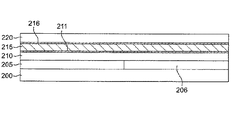
図1Bでは、ソース領域205および埋め込みコレクタ206の上に複数の材料層が形成される。一実施形態では、材料210、211、215、216および220の5層が、基板200のソース領域205および埋め込みコレクタ206の上に形成される。絶縁層210は、ソース領域205および埋め込みコレクタ206を、上に重なる層から電気的に分離する。したがって、絶縁層210は、この絶縁の目的に合致する材料から構成され、絶縁の目的に整合する厚みを有する。適当な材料の例には、ドープト酸化シリコンが含まれる。ドープト絶縁層の使用は、絶縁層210もドーパント・ソースとしての役割を果たして、後で説明するように、引き続き形成されるMOSFETデバイスのソース/ドレイン拡張部に、固相拡散プロセスによってドープするような実施形態で有利である。二酸化シリコン・ドーピング・ソースの一例は、PSG(リンガラス、すなわちリンドープト酸化シリコン)またはBSG(ボロン・ガラス、すなわちボロン・ドープト酸化シリコン)である。当分野の技術者なら、基板上にPSGまたはBSGの層を形成する適当な手段、例えば、プラズマ増速化学気相成長法(PECVD)を知っている。絶縁層210の適当な厚みは、約25nmから約250nmの範囲である。絶縁層210は、1×1021/cm3のオーダーの高いドーパント濃度を有する。
【0021】
絶縁層210の上に、エッチ・ストップ層211を形成する。エッチ・ストップは、当分野の技術者に知られているように、エッチングが下にある層または上に重なる層に進行するのを防止することを意図している。したがって、エッチ・ストップは、選択されたエッチング液に対して、隣接層より著しく大きな耐エッチング性を有する。具体的にこの場合は、選択されたエッチング液に対して、エッチ・ストップ層211のエッチング速度は、後述する犠牲層である上に重なる層のエッチング速度よりずっと遅い。本発明によれば、二酸化シリコン(例えば、テトラエチレンオルソシリケート(TEOS)から形成された二酸化シリコン)の犠牲層の除去のために、下にある層に対するエッチング液の作用を制限する適当なエッチ・ストップ材料が選択される。窒化シリコン(Si3N4)はこうした適当なエッチ・ストップ材料である。
【0022】
エッチ・ストップ層211の厚みは、エッチング工程で取り除かれる材料の深さに対して、選択されたエッチング液に対するエッチ・ストップ材料の抵抗性がどの程度であるかで決まる。エッチング液が下にある層に作用するのを防ぐことに加えて、エッチ・ストップ層211は、固相拡散工程中にソース/ドレイン拡張部を作るのに用いられたドーパントの、下方への拡散に対するオフセット・スペーサおよび拡散バリヤの役割も果たし、これによりゲートに対するソース/ドレイン拡張部の間隔および長さを画定する。エッチ・ストップ層211は、約5nmから約50nmの範囲の厚みを有する。
【0023】
エッチ・ストップ層211の上に、(例えば、TEOSプロセスによって)犠牲層215を形成する。後続の処理ステップ中に、犠牲層215を除去し、犠牲層215が空けたスペースにMOSFETゲートを形成する。したがって、犠牲層215の絶縁材料は、エッチング液が、エッチ・ストップ層211と比べて、犠牲層215を除去するために著しく高い選択性を有するように選ばれる。犠牲層215の厚みは、最終MOSFETデバイスのチャネル長に対応するように選ばれる。二酸化シリコンは、犠牲層215の適当な半導体材料の一例である。
TEOSプロセスでは、一般に、酸素雰囲気中、650℃から750℃での化学気相成長(CVD)によって、気化した液体TEOS(テトラエチルオルソシリケート前駆体(Si(OC2H5)4)が分解してシリコン酸化膜(TEOS堆積酸化物と呼ばれる)の形成が起こる。こうしたTEOS堆積は、良好な均一性およびステップ・カバレッジを実現することが知られている。一般に、この堆積膜は、二酸化シリコンと呼ばれることが多いが、シリコンの非化学量論的酸化物であることが分かっている。オゾン(O3)を、例えば反応酸素の10パーセントまで混ぜると、より低温での堆積が促進される。オゾンを含む代表的な反応は、400℃および300トルで、オゾン6パーセントを含む酸素を1分当たり4標準リットル(slm)、Heを1.5slm、およびTEOSを1分当たり300標準立方センチメートル(sccm)として行われる。
【0024】
エッチ・ストップ層216は、犠牲層215の上にも形成される。エッチ・ストップ層216は、層211の機能と同様な役割を果たし、例えば窒化シリコンで形成することができる。
【0025】
エッチ・ストップ層216の上に、絶縁層220を形成する。絶縁層220は、絶縁層210と同じエッチング速度(共通のエッチング液に対して)を有することが有利であるので、これらの層を同じ材料、例えばPSGまたはBSGから形成することが好ましく、したがって、これもまたMOSFETソース/ドレイン拡張部へのドーパント・ソースとしての役割を果たすことができる。
【0026】
層210、211、215、216および220のすべては、通常の化学気相成長法(CVD)プロセス、または他のよく知られた堆積技術を用いて堆積することができる。上記の層の順序については、他の実施形態が、大きな変更、例えば堆積層の減少を含んでもよいことにも留意しなければならない。いずれにせよ、得られる構造を用いてMOSFETデバイス用の一つの縦型チャネル領域と、BJTデバイス用の他の領域が形成される。
【0027】
図1Cを参照すると、開口、ウインドウ、またはトレンチ225および227が、絶縁層220、エッチ・ストップ層216、犠牲層215、エッチ・ストップ層211、および絶縁層210を通して、MOSFETのソース領域205およびBJTの埋め込みコレクタ領域206まで異方的にエッチングされている。ウインドウの水平寸法、すなわち図1Dの断面の水平寸法は、最終デバイスの所望の性能特性、加工されるデバイスのサイズ的制約、およびウインドウ225および227の形成に用いられるリソグラフィ工程の限界によって決まる。ウインドウ225および227の長さ、すなわち頁内部への距離も、主として設計選択事項である。ウインドウ225および227は、同寸法である必要は無い。所与のウインドウ水平寸法に対して、ウインドウ内に後で形成されるコンダクタの電流容量は、ウインドウ長さの増大と共に増加する。
【0028】
次いで、ウインドウ225および227は、化学洗浄工程(例えば、RCAまたはピランハ・クリーン)にかけて、ウインドウ225および227の底のシリコンを洗浄する。この洗浄ステップの結果、ウインドウ225および227との境界を形成している絶縁層210および220の小部分が除去される。得られたくぼみ228を図1Dに示す。こうして、犠牲層215およびエッチ・ストップ層211および216は、絶縁層210および220の端部を越えて延在する。
【0029】
図1Eを参照すると、デバイス品質の結晶性半導体材料(例えばシリコン)230および231を、それぞれウインドウ225および227内に形成する。使用可能な結晶性半導体材料の他の例には、シリコンゲルマニウムおよびシリコンゲルマニウム炭素がある。結晶性半導体材料をウインドウ内に形成する技術は、当分野の技術者にはよく知られている。例えば、結晶性半導体材料は、エピタキシャルに(すなわち、それぞれソース領域205および埋め込みコレクタ領域206から成長させて)または堆積させて、ウインドウ225および227内に形成することができる。他の実施形態では、基板200全体上にアモルファス・シリコンを堆積させ、ウインドウ225および227、ならびに各ウインドウ上端の頭部232および233を除いてすべてを除去する。次いでアモルファス・シリコンは、例えばレーザーでアニールしてこれを再結晶化する。
【0030】
ウインドウ225内の結晶性半導体材料またはプラグ230には、ドープしてMOSFETチャネルを形成し、かつ反対にドープしたソースおよびドレイン拡張部を形成しなければならない。但し、一般に後者はプロセスの後方で形成される。チャネル領域を形成するために結晶性半導体材料230をドーピングする各種の周知技術は適当である。エピタキシャル成長または堆積による形成中のIn−situドーピング、または形成後の結晶性半導体材料230中へのドーパントの注入は、チャネル領域を形成する適当な方法である。In situ、すなわち化学気相成長法で材料の層が形成されるときのドーパント導入は、よく知られており本明細書では詳細に説明しない。一般に、ドーパントは、堆積工程の適当な点で雰囲気中に導入されて所望の濃度を形成する。これらの技術はいずれも、BJTの結晶性半導体材料231の、二つの反対にドープされた領域の形成にも適用することができる。
【0031】
結晶性半導体材料230および231は、ドープされていない状態で成長または堆積し、次いで注入によってドーピングすることもできる。BJT用の結晶性半導体材料231は、2つのドーパント型を含む。すなわち、頭部領域235はベースを形成し、したがって下にあるコレクタ領域234とは反対のドーパント型を有するので、2つの注入ステップが必要になる。第1ステップでは、両領域234および235には、イオン注入によって第1ドーパント型をドープする。次いで、適当なエネルギーでイオンを注入することによって反対にドーピングして、領域234のドーパントを第1ドーパント型から第2ドーパント型へ変えてベース領域235を形成し、一方、下にあるベース領域234は、第1ドーパント型でドーピングされたままである。代表的な最終ドーパント濃度は、エミッタについては1×10¹⁹から5×10²⁰/cm3、ベースについては1×1017/cm3、およびコレクタについては1×1016/cm3である。MOSFET用チャネルの底部にソース/ドレイン拡張部を形成するためには、基板200から結晶性半導体材料230の底部へドーパントを拡散することができる。イオン注入も、結晶性半導体材料230の頭部にソース/ドレイン拡張部領域を作るための適当な手段である。また下記に詳述するように、隣接する絶縁層からソース/ドレイン拡張部の領域にドーパントを拡散するために固相拡散を用いることもできる。
【0032】
さらに他の実施形態では、ウインドウ227の2つのBJT領域234および235に異なる半導体材料を用いることが所望される。このときは、次に他の材料をその中に堆積させることができるように、成長エピタキシャル層が完全にウインドウ227を充填しないようにする。当分野の技術者なら分かるように、この実施形態に従ってウインドウ227に異なる材料を形成させるには、他のウインドウで何らかの加工ステップが行われている間は、ウインドウ225と227を交互にマスキングすることが必要である。
【0033】
結晶性半導体材料230および231にドープし、ドーパントがその中に所望どうりに分布した後は(ある実施形態では、ソースおよびドレイン拡張部は、プロセスのこの点ではまだ形成されていない)、基板には、ドーパントの分布に著しく影響を与える条件を施すべきではない。このステップの後、1100℃を超える温度に基板をさらさないことが、必ずしもではないが、好ましい。実際、プロセスのこの点の後、1000℃を超える温度に基板をさらさないことが有利である。ある実施形態では、基板は、900℃を超える温度に長時間(例えば、数分を超えて)さらさない。しかし、基板に、約1000℃の温度で、ドーパントの分布に悪影響を与えずに瞬時熱アニールを施すことができる。別法として、所望のドーパント分布を生じさせるように、この後の高温処理を計画することもできる。
【0034】
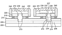
結晶性半導体材料230および231の頭部232および233は、例えば化学的/機械的研摩によって除去される。この工程の結果、図1Fに示したように、結晶性半導体材料230および231の上面と絶縁層220とが平坦化される。同様に図1Fに示したように、ベース領域235に隣接する絶縁層の領域上に、窒化シリコン層236を形成する。窒化層236は、今後形成されるエミッタを、絶縁層220のBSG材料からのp型固相拡散から分離することが好ましい。ベース領域235にアクセスするために、窒化シリコン層236にウインドウ237をエッチングする。これらのプロセス・ステップの間、MOSFETデバイスはマスクされる。
【0035】
絶縁層220および窒化シリコン層236を含めた構造全体の上に、共形層238を形成する。層238は、MOSFETの自己整合頭部コンタクト(この実施形態ではドレイン・コンタクト)を提供する。層238の適当な材料の1例は、ドープト多結晶シリコンであり、この場合ドーパントの型は、MOSFETチャネル・ドーパントと反対である。層238のドーパントの濃度は、約1×10²⁰原子/cm3より高い。
【0036】
図1Gにさらに示したように、層238の上に共形層239を堆積する。層239用に選ぶ材料は、犠牲層215のエッチング速度より著しく遅いエッチング速度を有するように選ぶ。好ましくは、239用に選ぶ材料は、エッチ・ストップ層211および216の材料と同じである。適当な材料の1例は窒化シリコンである。層239は、既知の技術を用いて層238の上に形成される。
【0037】
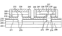
通常のリソグラフィ技術を用いて、層238、層239および絶縁層220をパターン化し、残る部分が結晶性半導体材料230またはベース235の上に重なる部分または隣接部だけとなるように、(1つまたは複数のドライ・エッチ・ステップを用いて)エッチングする。図1Hを参照されたい。ここで、BJTのエミッタは参照符合241で呼ばれ、MOSFETのドレインは参照符合242で呼ばれる。
【0038】
一実施形態では、プロセスのこの点で、上記のようにPSGまたはBSG材料から形成されている絶縁層210および220からの固相拡散によってソース/ドレイン拡張部を形成する。ドーパントは、絶縁層210および220からの固相拡散によって、結晶性半導体材料230および231内に移動させられて、MOSFETのソース拡張部270およびドレイン拡張部272、およびBJTの領域拡張部274を形成する。固相拡散では、酸化物(例えば、二酸化シリコン)はドーパント・ソースとしての役割を果たす。高温で、ドーパントは、結晶性半導体材料230および231のドープされた酸化物から隣接のドープされてない(またはわずかにドープされた)領域に移動させられる。ドープされる領域が、結晶性半導体材料230および231と、ドーパント・ソースとしての役割を果たす絶縁層210および220の間の界面によって画定されているので、この技術は有利である。この技術は、自己整合ソース/ドレイン拡張部(すなわち、ソース・ドレイン拡張部がゲートと整合している)の形成を可能にする。固相拡散技術の例は、Ono,M等「Sub−50nm Gate Length N−MOSFETS with 10nm Phosphorus Sourceand Drain Junctions」、IEDM 93、119〜122頁(1993年)、およびSaito,M等「An SPDD D−MOSFET Structure Suitable for 0.1 and Sub 0.1 Micron Channel Length and Its Electrical Characteristics」、IEDM 92、897〜900頁(1992年)に記載されており、これらを参照により本明細書に組み込む。
【0039】
絶縁層210および220からドープされる結晶性半導体材料230部分のドーパントの濃度は、一般に、少なくとも約1×10¹⁹/cm3であり、約5×1019/cm3のドーパント濃度が有利であると考えられる。この固相拡散技術を用いて、非常に浅いソースおよびドレイン拡張部270/272を得ることができる。ソース拡張部270およびドレイン拡張部272は、結晶性半導体材料230内部へ、好ましくは結晶性半導体材料230の幅の半分未満まで浸透していることが示されている。このようにドーパントの浸透を制限することにより、結晶性半導体材料230の反対側からチャネル領域で重なる可能性が回避される。さらに、ソース拡張部270およびドレイン拡張部272がゲート誘電体250の下へ延在する距離は、ゲート長の4分の1未満に制限されることが好ましい。この距離は、オフセット・スペーサとしての役割を果たすエッチ・ストップ層211および216の厚みによって制御することができる。当分野の技術者なら周知のように、ソース拡張部270およびドレイン拡張部272のドーパントは、結晶性半導体材料230のチャネル260のドーパントとは反対の型である。
【0040】
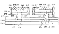
図1Iに示したように、次いで共形層240を堆積する。所与のエッチ化学反応に対して、層240の材料は、犠牲層215のエッチング速度より著しく遅いエッチング速度であるように選ぶ。層240の適当な材料の一例は窒化シリコンである。層240の厚みは、ドレイン242、エミッタ241、層239および絶縁層220の残る部分が、その後のエッチング液との接触から保護されるように選ばれる。
【0041】
次いで、ドライ・プラズマ・エッチングなどの異方性エッチングを用いて層240をエッチングする。これによりエッチ・ストップ層216の一部分が除去される。したがって、図1Jに示したように、異方性エッチング後に残る層240の部分は、絶縁層220、ドレイン242、エミッタ241、および層239の横に隣接する側壁のみである。このエッチング工程の結果、エッチ・ストップ層211の一部が除去され、ここで犠牲層215が露出する。
【0042】
次いで、デバイスに、ウエット・エッチング(例えば、水性フッ化水素酸)または等方性ドライ・エッチング(例えば、無水フッ化水素酸)を施す。これにより、犠牲層215の露出残存部分が除去される。結果を図1Kに示す。ここでは、絶縁層210は、エッチ・ストップ層211にまだ覆われている。絶縁層220およびドレイン242は、エッチ・ストップ層216、ならびに層239および240の残存部分によって包まれている。したがって、絶縁層210および220、ならびにドレイン242の残存部分は、その後のエッチング手段との接触から分離されている。犠牲層215の除去によって露出した結晶性半導体材料230の領域は、MOSFETデバイスの物理的チャネル長を画定する。さらに、BJT領域内のエミッタ241および絶縁層220は、層239および240、ならびにエッチ・ストップ層216によって保護されている。
【0043】
図1Lを参照すると、熱二酸化シリコンの犠牲層245を、結晶性半導体材料230および231(後者がコレクタ領域234およびベース領域235を含む)の露出表面上に、約10nm未満のオーダーの厚みまで成長させる。犠牲二酸化シリコン245を、通常の等方性エッチング(例えば、水性フッ化水素酸)を用いて除去する(図1M参照)。犠牲二酸化シリコン245の形成および除去の結果、結晶性半導体材料230および231各々の表面は、より滑らかになり側壁欠陥のいくつかは除去される。エッチ・ストップ層211および216は、この手段が絶縁層210および220、ならびにドレイン242に接触することを防ぐ。このステップは必要ないが、結晶性半導体材料230および231に過度の欠陥がある場合には、これを含めることが望ましいであろう。
【0044】
次いで、ゲート誘電体またはゲート酸化膜の層250を、結晶性半導体材料230および231の露出部分に形成する。図1Nを参照されたい。適当な誘電体材料には、例えば、熱成長二酸化シリコン、酸窒化シリコン、窒化シリコンまたは金属酸化物が含まれる。ゲート誘電体250の厚みは、約1nmから約20nmである。適当な厚みの一例は6mmである。一実施形態では、酸素含有雰囲気で約700℃から約1000℃の範囲の温度に基板を加熱することによって、二酸化シリコン層を形成する。ゲート誘電体250を形成する他の手段には、化学気相成長法、ジェット蒸着法、原子層堆積法があり、これらすべてが適当であると思われる。所望の厚みのゲート誘電体250を形成する条件は、当分野の技術者にはよく知られている。
【0045】
図1Oを参照すると、ゲートは、十分共形で適当なゲート材料からなる層255(例えば、ドーパントをin situで導入し、次いで再結晶化して多結晶シリコンを形成したドープト・アモルファス・シリコンの層)を堆積することによってゲート誘電体250の周辺に形成される。好ましくは、このステップは、結晶性半導体材料230および231のドーパントのドーパント・プロフィルに著しい影響を与えない条件で行われる。適当なゲート電極材料の他の例には、ドープト多結晶シリコン、ドープト・シリコン・ゲルマニウム、およびドープト・シリコン・ゲルマニウム炭素がある。適当に低い抵抗率を有し、ゲート誘電体250の材料および他の半導体処理ステップと適合する金属および金属含有化合物も、適当なゲート材料であると考えられる。こうした金属の例には、チタン、窒化チタン、タングステン、タングステン・シリサイド、タンタル、窒化タンタル、およびモリブデンが含まれる。ゲート材料が、半導体プラグ材料230のバンド・ギャップほぼ中央近くの仕事関数を有すると有利である。ゲートを形成する適当な手段には、化学気相成長法、電気めっき法、およびこれらの組合せが含まれる。
【0046】
図1Pを参照すると、層255をパターン化して、MOSFETデバイスのゲート265およびBJTデバイスの制御端子266を形成する。ゲート265の配置は、主として設計選択事項である。ゲート265は、MOSFETのチャネル260を形成する結晶性半導体材料230およびゲート酸化膜250を囲んでいる。BJTの領域では、制御端子266を所望によりパターン化し、フローティングさせておく(すなわち、他の導電層と接続しない)か、この頁面外の第3次元での配線によって、ベース領域235と接続することができる。
【0047】
図1Qは、完成した構造を示す。MOSFETドレイン242へのアクセスは、絶縁層239にウインドウをエッチングすることによって実現される。BJTエミッタ241には、層255および絶縁層239にウインドウをエッチングすることによってアクセスする。MOSFETソース領域205およびBJT埋め込みコレクタ領域206の両方には、図1Q断面の面外の第3次元でアクセスする。BJTベース領域235へも、第3次元でアクセスする。
【0048】
さらに他の実施形態では、ドープされていない二酸化シリコンの薄層(例えば、厚み約25nm)を、ソース領域205の上に形成する。図1Eを参照すると、この層(示さず)は、絶縁層210(ドーパント・ソース)から下へソース領域205を通過し、次いで、結晶性半導体材料230が形成されると、上の結晶性半導体材料230へと拡散する、望ましくない固相拡散へのバリヤとして働く。
【0049】
本発明の教示により、上述の加工プロセス・フローに従って組み立てられたNPN BJTの断面図を図2に示す。図2に示した層および領域は、それぞれ図1Aから1Qの同じ番号の層および領域に対応する。この例では、エミッタ241にはn+をドープし、ベース235にはpをドープし、コレクタ領域234にはnをドープし、埋め込みコレクタ206にはn+をドープしている。こうして、通常のNPN BJTトランジスタが形成されている。NMOS VRGデバイスの加工により、PNP BJTトランジスタの形成が可能になる。したがって、PMOSおよびNMOS VRGデバイスの両方を有するCMOS集積回路では、本発明の教示に従って、プロセス・フローに追加のステップをほとんど必要とせずに、NPNおよびPNPトランジスタの両方を形成することができる。MOSFETのソースおよびドレイン拡張部270および272の形成と同時に、BJTに拡張部274が形成される。拡張部274は、BJTの動作には必要ないが、有害作用はない。MOSFETの酸化膜と同時に形成される酸化膜250は、コレクタ234とベース235がゲート255を経由して短絡するのを防止する。
【0050】
有利には、一実施形態では、BJTの制御端子266は、分離した導電領域を形成する。この領域には、電圧を印加することができ、したがって酸化膜250と共に働くと、電界効果作用、すなわち電界効果領域内の可動電荷キャリアのデプリーション、反転、またはアキュムレーションによってバイポーラ接合トランジスタのある種の性能特性を制御または修正することができる。例えば、層制御端子266への適当な電圧の印加により、コレクタ領域234およびベース領域235内にデプリーション領域を形成することができる。こうして、印加電圧は、コレクタ234およびベース235を通る電流を制御する。印加電圧は、BJTの耐圧または利得(すなわち、BJTの出力動力に対する入力動力の割合)の制御にも用いることができる。MOSFETのゲートのように、制御端子は、高い入力インピーダンスを示す。
【0051】
上記の実施形態は、本発明を用いたプロセスの具体例を例示するために提供される。当分野の技術者なら、本発明を実施するために有用な、多くのプロセス・シーケンス、材料、および手段があることを理解するであろう。本発明は、頭記の特許請求の範囲と整合性がある点以外は、例示した例に限定されるものではない。
【図面の簡単な説明】
【図1A】順次加工ステップ中の、本発明の一実施形態による回路構造の断面図である。
【図1B】順次加工ステップ中の、本発明の一実施形態による回路構造の断面図である。
【図1C】順次加工ステップ中の、本発明の一実施形態による回路構造の断面図である。
【図1D】順次加工ステップ中の、本発明の一実施形態による回路構造の断面図である。
【図1E】順次加工ステップ中の、本発明の一実施形態による回路構造の断面図である。
【図1F】順次加工ステップ中の、本発明の一実施形態による回路構造の断面図である。
【図1G】順次加工ステップ中の、本発明の一実施形態による回路構造の断面図である。
【図1H】順次加工ステップ中の、本発明の一実施形態による回路構造の断面図である。
【図1I】順次加工ステップ中の、本発明の一実施形態による回路構造の断面図である。
【図1J】順次加工ステップ中の、本発明の一実施形態による回路構造の断面図である。
【図1K】順次加工ステップ中の、本発明の一実施形態による回路構造の断面図である。
【図1L】順次加工ステップ中の、本発明の一実施形態による回路構造の断面図である。
【図1M】順次加工ステップ中の、本発明の一実施形態による回路構造の断面図である。
【図1N】順次加工ステップ中の、本発明の一実施形態による回路構造の断面図である。
【図1O】順次加工ステップ中の、本発明の一実施形態による回路構造の断面図である。
【図1P】順次加工ステップ中の、本発明の一実施形態による回路構造の断面図である。
【図1Q】順次加工ステップ中の、本発明の一実施形態による回路構造の断面図である。
【図2】本発明の一実施形態によるバイポーラ接合トランジスタ構造の断面図である。[0001]
BACKGROUND OF THE INVENTION
The present invention is directed to semiconductor devices incorporating junctions of different conductivity types and methods of making such devices. More specifically, the present invention relates to bipolar junction transistor devices and methods for processing integrated circuits incorporating such devices.
[0002]
[Prior art]
Increasing semiconductor device performance and increasing device density (number of devices per unit area) have been important objectives in the semiconductor industry. Device density is increased by making individual devices smaller and packing devices more densely. However, as device dimensions (also called feature sizes or design rules) become smaller, the method of forming the device and its components must be adapted. For example, production line feature sizes are currently in the range of 0.25 microns to 0.12 microns, and the trend of miniaturization is unchanging. However, as device dimensions shrink, some manufacturing limitations arise, especially in the lithography process. In fact, current lithographic processes are approaching the point that devices cannot be fabricated accurately with the minimum size required by today's device users.
[0003]
Currently, most metal oxide semiconductor field effect transistors (MOSFETs) are formed in a lateral arrangement, and current flows parallel to the main surface or body surface of the substrate. As the size of these MOSFET devices decreases and the device density increases, the difficulty of the processing process also increases. In particular, the lithography process for creating the channel is problematic because the wavelength of the radiation used to image the lithographic pattern is approaching the device dimensions. Therefore, for lateral MOSFETs, the gate length is approaching the point where it cannot be precisely controlled by lithography techniques.
[0004]
Due to recent advances in packaging density, various types of vertical MOSFETs have been obtained. In particular, vertical devices are described in Takato, H. et al. "Impact of Surrounding Gates Transistor (SGT) for Ultra-High-Density LSI's", IEEE Transactions on Electron Devices, 38 (3), pp. 573-577. Proposed as an alternative. Recently, MOSFETs characterized as vertical replacement gate transistors have been described. "The Vertical-Replacement Gate (VRG) MOSFET: A 50-nm Vertical MOSFET with Lithium-Independent Gate Length 19", Technical Digest of Int.
[0005]
In general, an integrated circuit has a plurality of active elements including MOSFETs, JFETs and bipolar junction transistors, and passive components such as resistors and capacitors. Shared US Pat. Nos. 6,027,975 and 6,197,641 teach certain techniques for fabricating vertical replacement gate (VRG) MOSFETs, and are hereby incorporated by reference. Incorporate into. Therefore, it is advantageous to fabricate bipolar junction transistors (BJTs) using compatible processing steps similar to those used in MOSFET processing to reduce the cost of fabricating integrated circuits.
[0006]
[Problems to be solved by the invention]
An architecture and processing process is provided for processing BJTs using processes compatible with vertical MOSFET processing.
[0007]
[Means for Solving the Problems]
According to one embodiment of the present invention, a semiconductor device has a first layer of semiconductor material and forms a first doped region therein. A plurality of semiconductor and insulating layers overlie the first doped region, and windows or trenches are formed in the plurality of layers. A second doped region of a conductivity type different from the first doped region overlaps the first doped region within the window. Also in the window, a third doped region having a conductivity type different from that of the second doped region overlaps the second region. The first region is a BJT collector region, and the second region is a base. The third region is an emitter.
[0008]
In a related fabrication method, an integrated circuit structure is processed by forming a semiconductor layer suitable for device formation and providing a first surface along the first surface. A plurality of layers are formed thereon, and windows are formed in the plurality of layers. In the BJT device, a first device region is formed in a semiconductor layer, and this device region is a collector. A base layer is formed on the collector layer and an emitter region is formed on the base. Both the base and emitter regions are formed in the window.
[0009]
According to the present invention, the BJT and the vertical MOSFET can be processed into the same semiconductor substrate by using a compatible processing process and adding a minimum number of processing steps. That is, both devices are formed from a plurality of shared insulating and semiconductor layers, and some of the active regions of each device are formed in multiple layers within the window.
[0010]
The invention will be more readily understood and further benefits and advantages of the invention will be more readily appreciated when considered with the description of the preferred embodiment and the following drawings.
[0011]
In accordance with common practice, the various described features are not drawn to scale but are drawn to emphasize specific features relevant to the present invention. Reference signs refer to the same elements for all drawings and tests.
[0012]
DETAILED DESCRIPTION OF THE INVENTION
With respect to transistor and integrated circuit processing, the term “major surface” refers to the surface of a semiconductor layer in which a plurality of transistors are processed in and around, for example, in a planar process. As used herein, the term “vertical” means substantially perpendicular to the major surface. In general, the main surface is along the <100> plane of the single crystal silicon layer in which the bipolar transistor device is processed. For MOSFETs, the term “vertical transistor” means a transistor in which individual semiconductor components are arranged perpendicular to the major surface, so that current flows vertically from drain to source. As an example, for a vertical MOSFET, the source, channel and drain regions are formed with an alignment that is relatively perpendicular to the major surface. With respect to BJT, the term “vertical transistor” means that the collector, base and emitter regions are formed with an alignment that is relatively perpendicular to the major surface. Collector refers to the portion of the semiconductor layer that performs the collector function of a bipolar transistor device, including current conduction and charge collection during transistor operation. If the electrical characteristics of the transistor do not change without such a region, adjacent regions of the same conductivity type are not included in the collector.
[0013]
The present invention is directed to a process for processing bipolar junction transistors (BJTs) using a process that is similar and compatible with the processing of vertical replacement gate metal oxide semiconductor field effect transistors (MOSFETs). According to one or more embodiments described herein, BJT and VRG transistors can be used in a manner that minimizes cost and processing complexity, eg, minimizes the number of additional mask steps for VRG formation. Thus, it is formed on a single silicon substrate. The present invention discloses BJT devices and fabrication processes that achieve these objectives.
[0014]
1A through 1Q show cross-sectional views of an
[0015]
A fabrication process for forming both VRGMOSFET and BJT is illustrated in FIGS. 1A through 1Q. In order to demonstrate the compatibility of processing both device types in a single processing process, the formation of both VRGMOSFET and BJT is illustrated. However, the present invention is not limited to embodiments in which vertical MOSFETs and BJTs are processed in a parallel arrangement or during the same process flow.
[0016]
While the various semiconductor features and regions described herein are preferably based on silicon semiconductor processing, other embodiments of the invention can be applied to different semiconductor materials, including compound semiconductors or heterojunction semiconductors, alone or in combination. May be based.
[0017]
Referring to FIG. 1A, a heavily doped
[0018]
After the heavily doped
[0019]
The depth of the heavily doped
[0020]
In FIG. 1B, multiple material layers are formed over
[0021]
An
[0022]
The thickness of the
[0023]
A
In the TEOS process, liquid TEOS (tetraethylorthosilicate precursor (Si (OC)) vaporized by chemical vapor deposition (CVD) at 650 ° C. to 750 ° C. in an oxygen atmosphere is generally used. 2 H 5 ) 4 ) Decomposes to form a silicon oxide film (referred to as TEOS deposited oxide). Such TEOS deposition is known to provide good uniformity and step coverage. In general, this deposited film, often referred to as silicon dioxide, has been found to be a non-stoichiometric oxide of silicon. Ozone (O 3 ) For example up to 10 percent of the reactive oxygen promotes lower temperature deposition. A typical reaction involving ozone is 4 standard liters per minute (slm) of oxygen containing 6 percent ozone, 1.5 slm of He, and 300 standard cubic centimeters per minute (sccm) of TEOS at 400 ° C. and 300 torr. ) Is done.
[0024]
An
[0025]
An insulating
[0026]
All of
[0027]
Referring to FIG. 1C, openings, windows, or
[0028]
The
[0029]
Referring to FIG. 1E, device quality crystalline semiconductor materials (eg, silicon) 230 and 231 are formed in
[0030]
The crystalline semiconductor material or plug 230 in the
[0031]
[0032]
In still other embodiments, it is desirable to use different semiconductor materials for the two
[0033]
After the
[0034]
The
[0035]
A
[0036]
As further illustrated in FIG. 1G, a
[0037]
Using conventional lithographic techniques,
[0038]
In one embodiment, at this point in the process, source / drain extensions are formed by solid phase diffusion from insulating
[0039]
The concentration of dopant in the
[0040]
A
[0041]
[0042]
The device is then subjected to wet etching (eg, aqueous hydrofluoric acid) or isotropic dry etching (eg, anhydrous hydrofluoric acid). Thereby, the exposed remaining portion of the
[0043]
Referring to FIG. 1L, a thermal silicon dioxide
[0044]
A gate dielectric or
[0045]
Referring to FIG. 1O, the gate is a
[0046]
Referring to FIG. 1P,
[0047]
FIG. 1Q shows the completed structure. Access to the
[0048]
In yet another embodiment, a thin layer of undoped silicon dioxide (eg, about 25 nm thick) is formed over the
[0049]
A cross-sectional view of an NPN BJT assembled according to the machining process flow described above in accordance with the teachings of the present invention is shown in FIG. The layers and regions shown in FIG. 2 correspond to the same numbered layers and regions in FIGS. 1A through 1Q, respectively. In this example,
[0050]
Advantageously, in one embodiment, the control of the
[0051]
The above embodiments are provided to illustrate specific examples of processes using the present invention. Those skilled in the art will appreciate that there are many process sequences, materials, and means useful for practicing the present invention. The present invention is not limited to the illustrated example except that it is consistent with the appended claims.
[Brief description of the drawings]
FIG. 1A is a cross-sectional view of a circuit structure according to an embodiment of the present invention during sequential processing steps.
FIG. 1B is a cross-sectional view of a circuit structure according to one embodiment of the present invention during sequential processing steps.
FIG. 1C is a cross-sectional view of a circuit structure according to one embodiment of the present invention during sequential processing steps.
FIG. 1D is a cross-sectional view of a circuit structure according to an embodiment of the present invention during sequential processing steps.
FIG. 1E is a cross-sectional view of a circuit structure according to an embodiment of the present invention during sequential processing steps.
FIG. 1F is a cross-sectional view of a circuit structure according to an embodiment of the invention during sequential processing steps.
FIG. 1G is a cross-sectional view of a circuit structure according to an embodiment of the present invention during sequential processing steps.
FIG. 1H is a cross-sectional view of a circuit structure according to an embodiment of the present invention during sequential processing steps.
FIG. 1I is a cross-sectional view of a circuit structure according to an embodiment of the present invention during sequential processing steps.
FIG. 1J is a cross-sectional view of a circuit structure according to an embodiment of the present invention during sequential processing steps.
FIG. 1K is a cross-sectional view of a circuit structure according to an embodiment of the present invention during sequential processing steps.
FIG. 1L is a cross-sectional view of a circuit structure according to an embodiment of the present invention during sequential processing steps.
FIG. 1M is a cross-sectional view of a circuit structure according to an embodiment of the present invention during sequential processing steps.
FIG. 1N is a cross-sectional view of a circuit structure according to an embodiment of the present invention during sequential processing steps.
FIG. 1O is a cross-sectional view of a circuit structure according to an embodiment of the present invention during sequential processing steps.
FIG. 1P is a cross-sectional view of a circuit structure according to one embodiment of the present invention during sequential processing steps.
FIG. 1Q is a cross-sectional view of a circuit structure according to an embodiment of the present invention during sequential processing steps.
FIG. 2 is a cross-sectional view of a bipolar junction transistor structure according to an embodiment of the present invention.
Claims (30)
半導体基板に、第1導電型をドープした埋め込みコレクタ領域(206)を形成するステップと、
前記半導体基板の埋め込みコレクタ領域の上に、順に、第1絶縁層(210)、犠牲層(215)、そして第2絶縁層(220)を形成するステップと、
前記第1絶縁層(210)、犠牲層(215)及び第2絶縁層(220)を通じて、前記埋め込みコレクタ領域が露出するように、ウインドウ(227)を形成するステップと、
前記ウインドウに、前記埋め込みコレクタ領域と接触し、前記第1導電型をドープしたコレクタ領域(234)と、第2導電型をドープしたベース領域(235)とを含む、ドープト半導体プラグ(231)を形成するステップと、
前記ドープト半導体プラグのベース領域の上に重なり、前記第1導電型をドープした、エミッタ領域(241)を形成するステップと、
エッチングプロセスにより、前記犠牲層を除去して、前記ドープト半導体プラグの一部を露出させるステップと、
前記ドープト半導体プラグの露出部にゲート誘電体(250)を形成するステップ、
前記犠牲層の除去によって生じた空間に、前記ゲート誘電体の周囲に、半導体材料または導電体材料を充填し、制御端子(266)を形成するステップと
を含む方法。A method of processing a vertical bipolar junction transistor,
Forming a buried collector region (206) doped with a first conductivity type in a semiconductor substrate;
Sequentially forming a first insulating layer (210), a sacrificial layer (215), and a second insulating layer (220) on the buried collector region of the semiconductor substrate;
Forming a window (227) through the first insulating layer (210), the sacrificial layer (215) and the second insulating layer (220) so that the buried collector region is exposed;
A doped semiconductor plug (231) in the window that includes a collector region (234) doped with the first conductivity type and a base region (235) doped with the second conductivity type in contact with the buried collector region; Forming step;
Forming an emitter region (241) overlying a base region of the doped semiconductor plug and doped with the first conductivity type;
Removing the sacrificial layer by an etching process to expose a portion of the doped semiconductor plug; and
Forming a gate dielectric (250) on an exposed portion of the doped semiconductor plug;
Filling the space created by the removal of the sacrificial layer with a semiconductor or conductor material around the gate dielectric and forming a control terminal (266).
前記半導体基板を加熱して前記第1絶縁層(210)および前記第2絶縁層(220)からドーパントを拡散させて、ドープト半導体プラグの隣接領域をさらにドープするステップをさらに含み、前記第1絶縁層(210)および前記第2絶縁層(220)のドープト二酸化シリコンの導電型が、ドープト半導体プラグに含まれるコレクタ領域の導電型と反対である、請求項1に記載の方法。 The material of the first insulating layer (210) and the second insulating layer (220) is doped silicon dioxide,
The method further comprises heating the semiconductor substrate to diffuse dopant from the first insulating layer (210) and the second insulating layer (220) to further dope adjacent regions of the doped semiconductor plug, the first insulating layer. The method of claim 1, wherein the conductivity type of the doped silicon dioxide of the layer (210) and the second insulating layer (220) is opposite to the conductivity type of the collector region included in the doped semiconductor plug.
半導体基板の主表面のMOSFETを形成する領域に、第1導電型をドープした第1ドープト領域(205)を形成するステップであって、前記第1ドープト領域がソース領域である、ステップ、
前記半導体基板の主表面の縦型バイポーラ接合トランジスタを形成する領域に、第2導電型をドープした埋め込みコレクタ領域(206)を形成するステップと、
前記第1ドープト領域及び埋め込みコレクタ領域上に、順に、第1絶縁層(210)、犠牲層(215)、そして第2絶縁層(220)を形成するステップと、
前記第1絶縁層(210)、犠牲層(215)、第2絶縁層(220)を通じて、前記MOSFETを形成する領域に、前記第1ドープト領域を露出するように第1ウインドウ(225)を形成し、前記縦型バイポーラ接合トランジスタを形成する領域に、前記埋め込みコレクタ領域を露出するように第2ウインドウ(227)を形成するステップと、
前記第1ウインドウに、第2の導電型でドープされた第1ドープト半導体プラグ(230)を形成し、前記第2ウインドウに、前記第2導電型をドープしたコレクタ領域(234)、および前記第1導電型をドープしたベース領域(235)を含み、該コレクタ領域が前記埋め込みコレクタ領域と接触している、第2ドープト半導体プラグ(231)を形成するステップと、
前記第1ドープト半導体プラグ上に第2ドープト領域(242)を、及び第2ドープト半導体プラグ上にエミッタ領域(241)を形成するステップであって、該第2ドープト領域がドレイン領域である、ステップ、
前記半導体基板を加熱することにより、前記第1絶縁層(210)及び第2絶縁層(220)からの固体拡散によって、該第1及び第2絶縁層(210,220)のドーパントが前記第1ドープト半導体プラグに移動することにより、該第1ドープト半導体プラグと該第1絶縁層(210)の隣接する領域に第1ドープト領域の拡張部(270)を、該第1ドープト半導体プラグと該第2絶縁層(220)の隣接する領域に第2ドープト領域の拡張部(272)を形成するステップと、
エッチングプロセスにより、前記犠牲層を除去し、それにより第1ドープト半導体プラグおよび第2ドープト半導体プラグの一部を露出するステップと、
前記第1ドープト半導体プラグの露出部及び第2ドープト半導体プラグの露出部上に、ゲート誘電体(250)を形成するステップと、
前記犠牲層の除去によって生じた空間に、前記ゲート誘電体の周囲に、半導体材料または導電体材料を充填することにより、前記MOSFETが形成される領域にゲート(265)を形成し、前記縦型バイポーラ接合トランジスタを形成する領域に制御端子(266)を形成するステップを含む方法。An integrated circuit structure processing method comprising:
Forming a first doped region (205) doped with a first conductivity type in a region for forming a MOSFET on a main surface of a semiconductor substrate, wherein the first doped region is a source region;
Forming a buried collector region (206) doped with a second conductivity type in a region for forming a vertical bipolar junction transistor on the main surface of the semiconductor substrate;
Forming a first insulating layer (210), a sacrificial layer (215), and a second insulating layer (220) in sequence on the first doped region and the buried collector region;
A first window (225) is formed through the first insulating layer (210), the sacrificial layer (215), and the second insulating layer (220) to expose the first doped region in a region where the MOSFET is to be formed. And forming a second window (227) in the region for forming the vertical bipolar junction transistor so as to expose the buried collector region;
The first window, the first to form a doped semiconductor plug (230) doped with a second conductivity type, the second window, the second conductive type doped collector region (234), and the first Forming a second doped semiconductor plug (231) including a base region (235) doped with one conductivity type, wherein the collector region is in contact with the buried collector region;
Forming a second doped region (242) on the first doped semiconductor plug and an emitter region (241) on the second doped semiconductor plug, wherein the second doped region is a drain region; ,
Wherein by heating the semiconductor substrate, the solid diffusion from the first insulating layer (210) and a second insulating layer (220), the dopant is the first of said first and second insulating layers (210, 220) by moving the doped semiconductor plug, extension of the first doped region adjacent the first region doped semiconductor plug and the first insulating layer (210) to (270), said first doped semiconductor plug and the second Forming an extension (272) of the second doped region in adjacent regions of the two insulating layers (220);
Removing the sacrificial layer by an etching process, thereby exposing a portion of the first doped semiconductor plug and the second doped semiconductor plug;
Forming a gate dielectric (250) on the exposed portion of the first doped semiconductor plug and the exposed portion of the second doped semiconductor plug;
The space created by the removal of the sacrificial layer is filled with a semiconductor material or a conductor material around the gate dielectric, thereby forming a gate (265) in a region where the MOSFET is to be formed. Forming a control terminal (266) in a region to form a bipolar junction transistor.
Applications Claiming Priority (2)
| Application Number | Priority Date | Filing Date | Title |
|---|---|---|---|
| US09/956,382 US6759730B2 (en) | 2001-09-18 | 2001-09-18 | Bipolar junction transistor compatible with vertical replacement gate transistor |
| US09/956382 | 2001-09-18 |
Publications (3)
| Publication Number | Publication Date |
|---|---|
| JP2003179067A JP2003179067A (en) | 2003-06-27 |
| JP2003179067A5 JP2003179067A5 (en) | 2005-11-04 |
| JP4797185B2 true JP4797185B2 (en) | 2011-10-19 |
Family
ID=25498168
Family Applications (1)
| Application Number | Title | Priority Date | Filing Date |
|---|---|---|---|
| JP2002270858A Expired - Fee Related JP4797185B2 (en) | 2001-09-18 | 2002-09-18 | Bipolar junction transistor compatible with vertical replacement gate transistor |
Country Status (5)
| Country | Link |
|---|---|
| US (1) | US6759730B2 (en) |
| JP (1) | JP4797185B2 (en) |
| KR (1) | KR100918779B1 (en) |
| GB (1) | GB2383190B (en) |
| TW (1) | TW569451B (en) |
Cited By (1)
| Publication number | Priority date | Publication date | Assignee | Title |
|---|---|---|---|---|
| US9209095B2 (en) | 2014-04-04 | 2015-12-08 | International Business Machines Corporation | III-V, Ge, or SiGe fin base lateral bipolar transistor structure and method |
Families Citing this family (38)
| Publication number | Priority date | Publication date | Assignee | Title |
|---|---|---|---|---|
| US6706603B2 (en) * | 2001-02-23 | 2004-03-16 | Agere Systems Inc. | Method of forming a semiconductor device |
| US6929983B2 (en) * | 2003-09-30 | 2005-08-16 | Cabot Microelectronics Corporation | Method of forming a current controlling device |
| DE102004055213B4 (en) * | 2004-11-16 | 2009-04-09 | Atmel Germany Gmbh | Method for producing an integrated circuit on a semiconductor chip |
| US7365016B2 (en) * | 2004-12-27 | 2008-04-29 | Dalsa Semiconductor Inc. | Anhydrous HF release of process for MEMS devices |
| JP2006310651A (en) * | 2005-04-28 | 2006-11-09 | Toshiba Corp | Method of manufacturing semiconductor device |
| US7714355B1 (en) * | 2005-12-20 | 2010-05-11 | National Semiconductor Corp | Method of controlling the breakdown voltage of BSCRs and BJT clamps |
| TWI305669B (en) * | 2006-07-14 | 2009-01-21 | Nanya Technology Corp | Method for making a raised vertical channel transistor device |
| DE102008047127B4 (en) * | 2008-05-30 | 2010-07-08 | Advanced Micro Devices, Inc., Sunnyvale | A method of fabricating integrally formed drain and source regions in a silicon germanium-containing transistor device and semiconductor device |
| US7820532B2 (en) * | 2008-12-29 | 2010-10-26 | Honeywell International Inc. | Methods for simultaneously forming doped regions having different conductivity-determining type element profiles |
| KR20110016325A (en) * | 2009-08-11 | 2011-02-17 | 삼성전자주식회사 | Semiconductor device and method of fabricating the same |
| GB201105953D0 (en) * | 2011-04-07 | 2011-05-18 | Metryx Ltd | Measurement apparatus and method |
| US9349902B2 (en) | 2012-06-01 | 2016-05-24 | Taiwan Semiconductor Manufacturing Company, Ltd. | System and method for reducing irregularities on the surface of a backside illuminated photodiode |
| KR20140026156A (en) * | 2012-08-24 | 2014-03-05 | 에스케이하이닉스 주식회사 | Access device and fabrication method thereof, and semiconductor memory device having the same |
| US9406793B2 (en) * | 2014-07-03 | 2016-08-02 | Broadcom Corporation | Semiconductor device with a vertical channel formed through a plurality of semiconductor layers |
| US9847233B2 (en) * | 2014-07-29 | 2017-12-19 | Taiwan Semiconductor Manufacturing Company Limited | Semiconductor device and formation thereof |
| US9716155B2 (en) * | 2015-12-09 | 2017-07-25 | International Business Machines Corporation | Vertical field-effect-transistors having multiple threshold voltages |
| US10217817B2 (en) | 2016-01-27 | 2019-02-26 | International Business Machines Corporation | Sacrificial layer for channel surface retention and inner spacer formation in stacked-channel FETs |
| US10096673B2 (en) | 2016-02-17 | 2018-10-09 | International Business Machines Corporation | Nanowire with sacrificial top wire |
| US9530866B1 (en) | 2016-04-13 | 2016-12-27 | Globalfoundries Inc. | Methods of forming vertical transistor devices with self-aligned top source/drain conductive contacts |
| US9799751B1 (en) | 2016-04-19 | 2017-10-24 | Globalfoundries Inc. | Methods of forming a gate structure on a vertical transistor device |
| US9640636B1 (en) | 2016-06-02 | 2017-05-02 | Globalfoundries Inc. | Methods of forming replacement gate structures and bottom and top source/drain regions on a vertical transistor device |
| US10170616B2 (en) | 2016-09-19 | 2019-01-01 | Globalfoundries Inc. | Methods of forming a vertical transistor device |
| US10347745B2 (en) | 2016-09-19 | 2019-07-09 | Globalfoundries Inc. | Methods of forming bottom and top source/drain regions on a vertical transistor device |
| US9859172B1 (en) * | 2016-09-29 | 2018-01-02 | International Business Machines Corporation | Bipolar transistor compatible with vertical FET fabrication |
| US9882025B1 (en) | 2016-09-30 | 2018-01-30 | Globalfoundries Inc. | Methods of simultaneously forming bottom and top spacers on a vertical transistor device |
| US9966456B1 (en) | 2016-11-08 | 2018-05-08 | Globalfoundries Inc. | Methods of forming gate electrodes on a vertical transistor device |
| KR20180066708A (en) * | 2016-12-09 | 2018-06-19 | 삼성전자주식회사 | Semiconductor device and method for manufacturing the same |
| US9935018B1 (en) | 2017-02-17 | 2018-04-03 | Globalfoundries Inc. | Methods of forming vertical transistor devices with different effective gate lengths |
| US10229999B2 (en) | 2017-02-28 | 2019-03-12 | Globalfoundries Inc. | Methods of forming upper source/drain regions on a vertical transistor device |
| US10014370B1 (en) | 2017-04-19 | 2018-07-03 | Globalfoundries Inc. | Air gap adjacent a bottom source/drain region of vertical transistor device |
| US10269800B2 (en) * | 2017-05-26 | 2019-04-23 | Taiwan Semiconductor Manufacturing Co., Ltd. | Vertical gate semiconductor device with steep subthreshold slope |
| US9991359B1 (en) * | 2017-06-15 | 2018-06-05 | International Business Machines Corporation | Vertical transistor gated diode |
| WO2019215808A1 (en) * | 2018-05-08 | 2019-11-14 | ユニサンティス エレクトロニクス シンガポール プライベート リミテッド | Method for manufacturing columnar semiconductor device |
| US10900952B2 (en) * | 2019-05-16 | 2021-01-26 | International Business Machines Corporation | Dual surface charge sensing biosensor |
| US11355585B2 (en) | 2019-10-01 | 2022-06-07 | Analog Devices International Unlimited Company | Bipolar junction transistor, and a method of forming a charge control structure for a bipolar junction transistor |
| US11563084B2 (en) | 2019-10-01 | 2023-01-24 | Analog Devices International Unlimited Company | Bipolar junction transistor, and a method of forming an emitter for a bipolar junction transistor |
| US11404540B2 (en) | 2019-10-01 | 2022-08-02 | Analog Devices International Unlimited Company | Bipolar junction transistor, and a method of forming a collector for a bipolar junction transistor |
| US11189701B1 (en) * | 2020-12-11 | 2021-11-30 | International Business Machines Corporation | Bipolar junction transistor with vertically integrated resistor |
Family Cites Families (30)
| Publication number | Priority date | Publication date | Assignee | Title |
|---|---|---|---|---|
| US4366495A (en) | 1979-08-06 | 1982-12-28 | Rca Corporation | Vertical MOSFET with reduced turn-on resistance |
| US4455565A (en) | 1980-02-22 | 1984-06-19 | Rca Corporation | Vertical MOSFET with an aligned gate electrode and aligned drain shield electrode |
| US4837606A (en) | 1984-02-22 | 1989-06-06 | General Electric Company | Vertical MOSFET with reduced bipolar effects |
| US4587713A (en) | 1984-02-22 | 1986-05-13 | Rca Corporation | Method for making vertical MOSFET with reduced bipolar effects |
| JPS6126261A (en) | 1984-07-16 | 1986-02-05 | Nippon Telegr & Teleph Corp <Ntt> | Vertical mosfet and manufacture thereof |
| US4786953A (en) | 1984-07-16 | 1988-11-22 | Nippon Telegraph & Telephone | Vertical MOSFET and method of manufacturing the same |
| JPS61269377A (en) * | 1985-05-24 | 1986-11-28 | Hitachi Ltd | Semiconductor device |
| US4764801A (en) * | 1985-10-08 | 1988-08-16 | Motorola Inc. | Poly-sidewall contact transistors |
| US4851362A (en) | 1987-08-25 | 1989-07-25 | Oki Electric Industry Co., Ltd. | Method for manufacturing a semiconductor device |
| IT1217323B (en) * | 1987-12-22 | 1990-03-22 | Sgs Microelettronica Spa | INTEGRATED STRUCTURE OF HIGH VOLTAGE BIPOLAR POWER TRANSISTOR AND LOW VOLTAGE POWER MOS TRANSISTOR IN THE "EMITTER SWITCHING" CONFIGURATION AND RELATED MANUFACTURING PROCESS |
| JPH01238166A (en) * | 1988-03-18 | 1989-09-22 | Fujitsu Ltd | Semiconductor device |
| US5342797A (en) | 1988-10-03 | 1994-08-30 | National Semiconductor Corporation | Method for forming a vertical power MOSFET having doped oxide side wall spacers |
| US5001533A (en) | 1988-12-22 | 1991-03-19 | Kabushiki Kaisha Toshiba | Bipolar transistor with side wall base contacts |
| US5208172A (en) | 1992-03-02 | 1993-05-04 | Motorola, Inc. | Method for forming a raised vertical transistor |
| US5252849A (en) * | 1992-03-02 | 1993-10-12 | Motorola, Inc. | Transistor useful for further vertical integration and method of formation |
| US5324673A (en) * | 1992-11-19 | 1994-06-28 | Motorola, Inc. | Method of formation of vertical transistor |
| JPH07161726A (en) * | 1993-12-08 | 1995-06-23 | Canon Inc | Bipolar transistor |
| US5484737A (en) * | 1994-12-13 | 1996-01-16 | Electronics & Telecommunications Research Institute | Method for fabricating bipolar transistor |
| JP2613029B2 (en) * | 1994-12-16 | 1997-05-21 | 財団法人韓国電子通信研究所 | Manufacturing method of super self-aligned vertical structure bipolar transistor |
| US5538908A (en) * | 1995-04-27 | 1996-07-23 | Lg Semicon Co., Ltd. | Method for manufacturing a BiCMOS semiconductor device |
| US5576238A (en) | 1995-06-15 | 1996-11-19 | United Microelectronics Corporation | Process for fabricating static random access memory having stacked transistors |
| US5668391A (en) | 1995-08-02 | 1997-09-16 | Lg Semicon Co., Ltd. | Vertical thin film transistor |
| US5683930A (en) | 1995-12-06 | 1997-11-04 | Micron Technology Inc. | SRAM cell employing substantially vertically elongated pull-up resistors and methods of making, and resistor constructions and methods of making |
| FR2756104B1 (en) * | 1996-11-19 | 1999-01-29 | Sgs Thomson Microelectronics | MANUFACTURE OF BIPOLAR / CMOS INTEGRATED CIRCUITS |
| US6133099A (en) | 1997-02-04 | 2000-10-17 | Nec Corporation | Vertical MOSFET and method of manufacturing thereof |
| US6297531B2 (en) | 1998-01-05 | 2001-10-02 | International Business Machines Corporation | High performance, low power vertical integrated CMOS devices |
| US6242775B1 (en) * | 1998-02-24 | 2001-06-05 | Micron Technology, Inc. | Circuits and methods using vertical complementary transistors |
| US6072216A (en) | 1998-05-01 | 2000-06-06 | Siliconix Incorporated | Vertical DMOS field effect transistor with conformal buried layer for reduced on-resistance |
| US6197641B1 (en) | 1998-08-28 | 2001-03-06 | Lucent Technologies Inc. | Process for fabricating vertical transistors |
| US6027975A (en) * | 1998-08-28 | 2000-02-22 | Lucent Technologies Inc. | Process for fabricating vertical transistors |
-
2001
- 2001-09-18 US US09/956,382 patent/US6759730B2/en not_active Expired - Lifetime
-
2002
- 2002-08-22 TW TW091119025A patent/TW569451B/en not_active IP Right Cessation
- 2002-08-30 GB GB0220210A patent/GB2383190B/en not_active Expired - Fee Related
- 2002-09-17 KR KR1020020056476A patent/KR100918779B1/en not_active IP Right Cessation
- 2002-09-18 JP JP2002270858A patent/JP4797185B2/en not_active Expired - Fee Related
Cited By (1)
| Publication number | Priority date | Publication date | Assignee | Title |
|---|---|---|---|---|
| US9209095B2 (en) | 2014-04-04 | 2015-12-08 | International Business Machines Corporation | III-V, Ge, or SiGe fin base lateral bipolar transistor structure and method |
Also Published As
| Publication number | Publication date |
|---|---|
| JP2003179067A (en) | 2003-06-27 |
| TW569451B (en) | 2004-01-01 |
| GB2383190B (en) | 2006-05-24 |
| US20030052721A1 (en) | 2003-03-20 |
| KR20030024626A (en) | 2003-03-26 |
| GB2383190A (en) | 2003-06-18 |
| KR100918779B1 (en) | 2009-09-23 |
| US6759730B2 (en) | 2004-07-06 |
| GB0220210D0 (en) | 2002-10-09 |
Similar Documents
| Publication | Publication Date | Title |
|---|---|---|
| JP4797185B2 (en) | Bipolar junction transistor compatible with vertical replacement gate transistor | |
| US7033877B2 (en) | Vertical replacement-gate junction field-effect transistor | |
| JP5579280B2 (en) | CMOS vertical replacement gate (VRG) transistor | |
| US6653181B2 (en) | CMOS integrated circuit having vertical transistors and a process for fabricating same | |
| JP5274490B2 (en) | Structure and fabrication method of capacitors that can be integrated with vertical replacement gate transistors | |
| KR100572647B1 (en) | Process for fabricating vertical transistors | |
| US6197641B1 (en) | Process for fabricating vertical transistors |
Legal Events
| Date | Code | Title | Description |
|---|---|---|---|
| A521 | Request for written amendment filed |
Free format text: JAPANESE INTERMEDIATE CODE: A523 Effective date: 20050916 |
|
| A621 | Written request for application examination |
Free format text: JAPANESE INTERMEDIATE CODE: A621 Effective date: 20050916 |
|
| A131 | Notification of reasons for refusal |
Free format text: JAPANESE INTERMEDIATE CODE: A131 Effective date: 20090721 |
|
| A521 | Request for written amendment filed |
Free format text: JAPANESE INTERMEDIATE CODE: A523 Effective date: 20091021 |
|
| A131 | Notification of reasons for refusal |
Free format text: JAPANESE INTERMEDIATE CODE: A131 Effective date: 20100112 |
|
| A601 | Written request for extension of time |
Free format text: JAPANESE INTERMEDIATE CODE: A601 Effective date: 20100412 |
|
| A521 | Request for written amendment filed |
Free format text: JAPANESE INTERMEDIATE CODE: A523 Effective date: 20100415 |
|
| A602 | Written permission of extension of time |
Free format text: JAPANESE INTERMEDIATE CODE: A602 Effective date: 20100415 |
|
| RD02 | Notification of acceptance of power of attorney |
Free format text: JAPANESE INTERMEDIATE CODE: A7422 Effective date: 20100427 |
|
| TRDD | Decision of grant or rejection written | ||
| A01 | Written decision to grant a patent or to grant a registration (utility model) |
Free format text: JAPANESE INTERMEDIATE CODE: A01 Effective date: 20110620 |
|
| A01 | Written decision to grant a patent or to grant a registration (utility model) |
Free format text: JAPANESE INTERMEDIATE CODE: A01 |
|
| A711 | Notification of change in applicant |
Free format text: JAPANESE INTERMEDIATE CODE: A712 Effective date: 20110712 |
|
| A61 | First payment of annual fees (during grant procedure) |
Free format text: JAPANESE INTERMEDIATE CODE: A61 Effective date: 20110712 |
|
| FPAY | Renewal fee payment (event date is renewal date of database) |
Free format text: PAYMENT UNTIL: 20140812 Year of fee payment: 3 |
|
| R150 | Certificate of patent or registration of utility model |
Free format text: JAPANESE INTERMEDIATE CODE: R150 |
|
| R250 | Receipt of annual fees |
Free format text: JAPANESE INTERMEDIATE CODE: R250 |
|
| R250 | Receipt of annual fees |
Free format text: JAPANESE INTERMEDIATE CODE: R250 |
|
| S111 | Request for change of ownership or part of ownership |
Free format text: JAPANESE INTERMEDIATE CODE: R313113 |
|
| S533 | Written request for registration of change of name |
Free format text: JAPANESE INTERMEDIATE CODE: R313533 |
|
| R350 | Written notification of registration of transfer |
Free format text: JAPANESE INTERMEDIATE CODE: R350 |
|
| R250 | Receipt of annual fees |
Free format text: JAPANESE INTERMEDIATE CODE: R250 |
|
| LAPS | Cancellation because of no payment of annual fees |