JP4792180B2 - Semiconductor device manufacturing method, substrate processing method, and substrate processing apparatus - Google Patents
Semiconductor device manufacturing method, substrate processing method, and substrate processing apparatus Download PDFInfo
- Publication number
- JP4792180B2 JP4792180B2 JP2001231330A JP2001231330A JP4792180B2 JP 4792180 B2 JP4792180 B2 JP 4792180B2 JP 2001231330 A JP2001231330 A JP 2001231330A JP 2001231330 A JP2001231330 A JP 2001231330A JP 4792180 B2 JP4792180 B2 JP 4792180B2
- Authority
- JP
- Japan
- Prior art keywords
- region
- monogermane
- substrates
- substrate processing
- reactor
- Prior art date
- Legal status (The legal status is an assumption and is not a legal conclusion. Google has not performed a legal analysis and makes no representation as to the accuracy of the status listed.)
- Expired - Lifetime
Links
Images
Landscapes
- Chemical Vapour Deposition (AREA)
Description
【0001】
【発明の属する技術分野】
本発明は、半導体デバイスの製造方法および基板処理装置に関し、特に、減圧CVD法(化学気相堆積法)によって、ポリまたはアモルファスシリコンゲルマニウムを成膜する半導体デバイスの製造方法、基板処理方法および基板処理装置に関する。
【0002】
【従来の技術】
IC、LSI等の半導体デバイスを製造する工程においては、減圧CVD法(化学気相堆積法)によって、基板上に薄膜を成膜することが行われている。そのような成膜工程の中の一つとして、減圧CVD法によって、ポリシリコンゲルマニウム膜をMOSトランジスタのゲート電極部分に形成することが試されている。
【0003】
従来、MOSトランジスタのゲート電極部分にはシリコンが使用されてきたが、近年のゲート絶縁膜の薄膜化に伴い、ゲートにバイアス電圧を印加した際のゲートの空乏化や、熱処理工程におけるドーパントの電極からチャネル部分への突き抜けが、デバイス特性を悪化させる大きな問題点となっていた。上記の問題点は、シリコンに代えてシリコンゲルマニウムを用いることによって大幅に改善されることが判明している。
【0004】
【発明が解決しようとする課題】
シリコンに代えてシリコンゲルマニウムを用いた場合、同じ成膜条件下(500℃)での成膜速度は、シリコンの場合と比較して、ゲルマニウム比率が20%の時で約6倍、ゲルマニウム比率が30%の時で約14倍に増加する。それに伴い、反応炉内を通過する際の反応ガスの消費量も増加し、その消費量の増加割合は、シリコンよりもゲルマニウムのほうが1cm3あたりの質量が2.3倍程度大きいため顕著である。ゲルマニウムの原料ガスであるモノゲルマンを反応炉下部から1本のノズルで炉内に供給した場合、モノゲルマンの消費により、反応炉内の上流側と下流側でガス濃度が顕しく異なり、膜厚およびゲルマニウム比率の面内・面間均一性は大幅に悪化する。
【0005】
本発明の目的は、上記課題を解決し、モノシランとモノゲルマンとを使用して、減圧CVD法によって、膜厚およびゲルマニウム比率の面内・面間均一性が良好なシリコンゲルマニウム膜を基板上に形成する半導体デバイスの製造方法、基板処理方法および基板処理装置を提供することである。
【0006】
【課題を解決するための手段】
上記課題を解決するために、本発明は、請求項1に記載のように、
反応炉内でボートにより複数枚の基板を垂直方向に積層支持する工程と、前記反応炉内にモノシランとモノゲルマンとを供給して、前記ボートにより積層支持された前記複数枚の基板上にシリコンゲルマニウム膜を成膜する工程と、を有し、前記シリコンゲルマニウム膜を成膜する工程では、前記モノゲルマンを長さの異なる複数本のノズルを用いて、前記反応炉内の前記複数枚の基板が存在する領域の垂直方向において異なる複数箇所から供給することを特徴とする半導体デバイスの製造方法を構成する。
【0007】
また、本発明は、請求項2に記載のように、
前記複数枚の基板が存在する領域は、トップ領域と、該トップ領域下方のセンタ領域と、該センタ領域下方のボトム領域とを含んでおり、前記シリコンゲルマニウム膜を成膜する工程では、前記モノゲルマンを前記トップ領域、前記センタ領域および前記ボトム領域のそれぞれの領域から供給することを特徴とする請求項1記載の半導体デバイスの製造方法を構成する。
また、本発明は、請求項3に記載のように、
前記シリコンゲルマニウム膜を成膜する工程では、前記モノゲルマンを前記反応炉内の前記複数枚の基板が存在する領域の下方からも供給することを特徴とする請求項1または2に記載の半導体デバイスの製造方法を構成する。
また、本発明は、請求項4に記載のように、
前記シリコンゲルマニウム膜を成膜する工程では、前記モノゲルマンを前記反応炉内の前記複数枚の基板が存在する領域の上流側からも供給することを特徴とする請求項1または2に記載の半導体デバイスの製造方法を構成する。
また、本発明は、請求項5に記載のように、
反応炉内でボートにより複数枚の基板を垂直方向に積層支持する工程と、前記反応炉内にモノシランとモノゲルマンとを供給して、前記ボートにより積層支持された前記複数枚の基板上にシリコンゲルマニウム膜を成膜する工程と、を有し、前記シリコンゲルマニウム膜を成膜する工程では、前記モノゲルマンを長さの異なる複数本のノズルを用いて、前記反応炉内の前記複数枚の基板が存在する領域の垂直方向において異なる複数箇所から供給することを特徴とする基板処理方法を構成する。
また、本発明は、請求項6に記載のように、
基板を処理する反応炉と、前記反応炉内にモノシランを供給する第1ノズルと、前記反応炉内にモノゲルマンを供給する第2ノズルと、前記反応炉内で複数枚の基板を垂直方向に積層支持するボートと、を有し、前記反応炉内にモノシランとモノゲルマンとを供給して、前記ボートにより積層支持された前記複数枚の基板上にシリコンゲルマニウム膜を成膜する処理を行う基板処理装置であって、前記第2ノズルは、前記モノゲルマンを前記反応炉内の前記複数枚の基板が存在する領域の垂直方向において異なる複数箇所から供給するよう、長さの異なる複数本のノズルで構成されることを特徴とする基板処理装置を構成する。
また、本発明は、請求項7に記載のように、
前記複数枚の基板が存在する領域は、トップ領域と、該トップ領域下方のセンタ領域と、該センタ領域下方のボトム領域とを含んでおり、前記第2ノズルは、前記モノゲルマンを前記トップ領域、前記センタ領域および前記ボトム領域のそれぞれの領域から供給するよう構成されることを特徴とする請求項6記載の基板処理装置を構成する。
また、本発明は、請求項8に記載のように、
前記第2ノズルは、前記モノゲルマンを前記反応炉内の前記複数枚の基板が存在する領域の下方からも供給するよう構成されることを特徴とする請求項6または7に記載の基板処理装置を構成する。
また、本発明は、請求項9に記載のように、
前記第2ノズルは、前記モノゲルマンを前記反応炉内の前記複数枚の基板が存在する領域の上流側からも供給するよう構成されることを特徴とする請求項6または7に記載の基板処理装置を構成する。
【0008】
【発明の実施の形態】
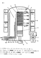
図1は、本発明の実施の形態例である基板処理装置の概要を示す。
【0009】
本発明の半導体デバイスの製造方法においては、反応ガスとしてモノシランとモノゲルマンとを使用し、反応炉11内において、減圧CVD法によって、基板であるウエハ4の上にシリコンゲルマニウム膜を成膜する半導体デバイスの製造方法において、図1に示すような長さの異なる多数本ノズル12a〜12eを通してモノゲルマンを炉内に供給することを特徴とする。
【0010】
本発明がなされる前の予備的考察において、膜厚およびゲルマニウム比率の面内・面間均一性を良好(3%以下)にするには、反応ガスの流れに沿って、成膜反応が始まる箇所から成膜が反応終わる箇所までの間で、モノシランガスおよびモノゲルマンガス、特に前述したようにモノゲルマンガスの消費を10%以下に保つことが必要であることが、経験上、認められている。
【0011】
モノゲルマンガスを反応炉11下部から1本のノズルで炉内に供給する形態で、モノゲルマンガスの消費を10%以下に保つために必要なモノゲルマン流量は、8インチウエハ用の内径26cmで高さが130cmの反応管内で、成膜される部分の表面積(反応管内壁およびウエハ表面)と実際の成膜速度(実験値)を考慮して見積もると、ゲルマニウム比率20%の場合約140sccmとなる。実際は安全のために反応ガスを10%程度に希釈して用いるので、1400sccmの希釈モノゲルマンを流すことになる。この時に必要なモノシラン流量はゲルマニウム比率20%で成膜温度が500℃の場合、約2800sccm(非希釈)である。ゲルマニウム比率をデバイス特性改善のためにもっと上げようとすると、前述したようにゲルマニウム比率を上げると成膜速度は速くなるので、ゲルマニウム比率30%の時に、モノゲルマンガスの消費を10%以下に保つために必要なモノゲルマンおよびモノシランの流量はそれぞれ500sccm(実際は5000sccmの希釈モノゲルマン)および5000sccm(非希釈)となり、このような大流量のガスを流して、反応炉内を一般的なプロセス圧力(30〜60Pa)にする場合には特大排気容量のポンプが必要であり現実的ではない。
【0012】
これらの計算結果から、多数本ノズルを用いてモノゲルマンを炉内に途中供給し、モノゲルマンの消費を、反応ガスの流れに沿って、成膜反応が始まる箇所から成膜が反応終わる箇所までの間で、10%以下に保つことが、膜厚およびゲルマニウム比率の面内・面間均一性が良好なシリコンゲルマニウム膜の形成を行う上で重要であるといえる。本発明は、このような考察に基づいてなされたものである。なお、このような条件下で形成されたシリコンゲルマニウム膜はポリシリコンゲルマニウム膜であるが、これとは異なる条件下ではアモルファスシリコンゲルマニウム膜が形成される場合もある。
【0013】
本発明に係る基板処理装置の一例として、反応ガスとしてモノシラン(SiH4)とモノゲルマン(GeH4)とを使用して、反応炉内でボートに複数枚のウエハを垂直方向に積層支持した状態で、炉体下部よりガスを導入し垂直方向に上昇させ、そのガスを用いたCVD法により、前記ウエハ上に薄膜を形成する減圧CVD装置の構造概略図を図1に示す。
【0014】
4ゾーンに分かれたヒータ6の内側に、反応炉11の外筒である石英製のアウターチューブ1およびアウターチューブ1内部の反応管であるインナーチューブ2が設置されており、この2種のチューブの間をメカニカルブースタポンプ7およびドライポンプ8を用いて真空引きしている。従って、インナーチューブ2内側に導入される反応ガスは、インナーチューブ2内を上昇し、2種のチューブ1、2の間を下降して排気される。ウエハ4が装填された石英ボート3はインナーチューブ2内に設置され、反応ガスにさらされた時に気相中およびウエハ4表面での反応により、ウエハ4上に薄膜が形成される。断熱板5はボート3と装置下部との間を断熱するためのものである。また、図1中、9はボート回転軸であり、10はステンレス製蓋である。
【0015】
なお、ボート3には、ウエハ4を支持するスロットが合計172個設けられており、一番下のスロットから数えて10スロット目まではダミーのウエハ4が、11から167スロット目までは製品のウエハ4が、168から172スロット目まではダミーのウエハ4が支持される。また、図1中のトップ領域、センタ領域、ボトム領域とは、それぞれ、129から167スロット目までの製品のウエハ4の存在する領域、37から128スロット目までの製品のウエハ4の存在する領域、11から36スロット目までの製品のウエハ4の存在する領域のことを示している。また、4つに分かれたヒータゾーンのうち、一番下のL(Lower)ゾーンは1スロット目より下側の、ウエハが殆ど存在しない領域に対応しており、下から二番目のCL(Center Lower)ゾーンは2から56スロット目までのダミーのウエハ4と製品のウエハ4とが混在する領域に対応しており、下から三番目すなわち上から二番目のCU(Center Upper)ゾーンは57から172スロット目までの製品のウエハ4とダミーのウエハ4とが混在する領域に対応しており、下から四番目すなわち一番上のU(Upper)ゾーンはそれより上側のウエハの存在しない領域に対応している。
【0016】
モノゲルマン(GeH4)を反応炉11内に供給する石英ノズル12a〜12eは長さが異なり、合計5本設けられており、12aはモノシラン(SiH4)を供給するノズルとともに炉口部(図中、左下)に設けられており、12b、12c、12d及び12eは、前記炉口部を通り、それぞれの噴出口が30スロット目、70スロット目、110スロット目及び150スロット目の位置に対応するように、設けられている。このような長さの異なる複数本ノズル12a〜12eを用いることによって、モノゲルマンを反応炉炉11内に途中供給することができる。
【0017】
また、断熱板5はLゾーンに対応するヒータ6よりも下側に設置される。
【0018】
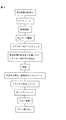
本発明に係る半導体デバイスの製造方法の一例として、図1に示した基板処理装置を用いる成膜手順を図2に示す。
【0019】
まず反応炉11内を成膜温度に安定化させた後、基板であるウエハ4を装填したボート3を反応炉11内にロード(挿入)する。リアクター(反応炉11)内を排気し、ボート3やチューブ1、2に吸着した水分等を脱離させるためにN2パージを行う。リアクター(反応炉11)内リークチェックを行った後、モノシランとモノゲルマンの流量を設定し、反応炉11内にガスを流して圧力を安定化させ成膜を行う。成膜が終了したら配管内をN2でサイクルパージし、N2でリアクター内を大気圧まで戻す。大気圧に戻ったらボート3をアンロードし、ウエハ4を自然冷却する。最後にウエハ4をボート3から取り出す。
【0020】
[実施の形態例]
(複数本ノズルを用いたモノゲルマンの途中供給)
図1に例示した基板処理装置において、長さの異なる複数本ノズルを用いてモノゲルマンを反応炉内に途中供給することで、膜厚およびゲルマニウム比率の面内・面間均一性が良好なポリシリコンゲルマニウム膜の形成が可能となる。
【0021】
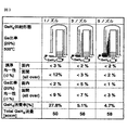
実際に実験を行った結果、得られた膜厚およびゲルマニウム比率の面内・面間均一性を、従来例をも含めて、モノゲルマン供給形態で比較して図3に示す。
【0022】
図3中、「1ノズル」は従来例に該当する形態であり、この場合に、モノゲルマンのノズルは1本のみであり、その噴出口はモノシランの噴出口の近くにある。これに対して、「3ノズル」と「5ノズル」とは本発明における形態であり、3ノズルの場合に、3本のモノゲルマンのノズルの噴出口はモノシランの噴出口の近くと、ボート3の70スロット目の近くと、150スロット目の近くとにあり、5ノズルの場合に、5本のモノゲルマンのノズルの噴出口はモノシランの噴出口の近くと、ボート3の30スロット目の近くと、70スロット目の近くと、110スロット目の近くと、150スロット目の近くとにある。各噴出口からは、ほぼ等量のモノゲルマンが噴出するようになっている。
【0023】
成膜温度は500℃、気相圧力は30Pa、ゲルマニウム比率は20%であり、モノゲルマンの(非希釈)全流量は、図3最下行(Total GeH4 流量で表示)に示したように、1ノズルの場合に50sccm、3ノズルおよび5ノズルの場合に58sccmである。モノシランおよびモノゲルマンは水素によって約10倍に希釈されて反応炉に供給される。
【0024】
実験の結果得られた膜厚の面内・面間均一性およびゲルマニウム比率(Ge比率と表示)の面内・面間均一性は図中に示されている。
【0025】
図3から明らかなように、多数本ノズルを用いてモノゲルマンを炉内に供給することで、1本のノズルのみで供給する形態(従来例)と比較して、大幅に膜厚およびゲルマニウム比率の面内・面間均一性が改善されていることが分かる。
【0026】
【発明の効果】
本発明の実施によって、モノシランとモノゲルマンとを使用して、減圧CVD法によって、膜厚およびゲルマニウム比率の面内・面間均一性が良好なシリコンゲルマニウム膜を基板上に形成する半導体デバイスの製造方法、基板処理方法および基板処理装置を提供することができる。
【図面の簡単な説明】
【図1】本発明に係る、反応ガスとしてモノシラン(SiH4)とモノゲルマン(GeH4)とを使用して薄膜を形成する減圧CVD装置の構造概略図である。
【図2】減圧CVD法による成膜手順を説明する図である。
【図3】膜厚およびゲルマニウム比率の面内・面間均一性の、モノゲルマン供給形態での比較を示す図である。
【符号の説明】
1…アウターチューブ、2…インナーチューブ、3…ボート、4…ウエハ、5…断熱板、6…ヒータ、7…メカニカルブースタポンプ、8…ドライポンプ、9…ボート回転軸、10…ステンレス製蓋、11…反応炉、12a〜12e…ノズル。[0001]
BACKGROUND OF THE INVENTION
The present invention relates to a semiconductor device manufacturing method and a substrate processing apparatus, and more particularly to a semiconductor device manufacturing method , a substrate processing method, and a substrate processing for forming a poly or amorphous silicon germanium film by low pressure CVD (chemical vapor deposition). Relates to the device.
[0002]
[Prior art]
In a process of manufacturing a semiconductor device such as an IC or LSI, a thin film is formed on a substrate by a low pressure CVD method (chemical vapor deposition method). As one of such film forming steps, it has been tried to form a polysilicon germanium film on the gate electrode portion of the MOS transistor by a low pressure CVD method.
[0003]
Conventionally, silicon has been used for the gate electrode portion of the MOS transistor. However, with the recent thinning of the gate insulating film, the gate electrode is depleted when a bias voltage is applied, and the dopant electrode is used in the heat treatment process. The penetration from the channel to the channel portion has been a major problem that deteriorates the device characteristics. It has been found that the above problems are greatly improved by using silicon germanium instead of silicon.
[0004]
[Problems to be solved by the invention]
When silicon germanium is used instead of silicon, the film formation rate under the same film formation conditions (500 ° C.) is about 6 times the germanium ratio when the germanium ratio is 20% compared to the case of silicon. It increases about 14 times at 30%. Along with this, the amount of reaction gas consumed when passing through the reactor also increases, and the rate of increase in consumption is remarkable because germanium has a mass per cm 3 larger than silicon by about 2.3 times. . When monogermane, which is the source gas of germanium, is supplied into the furnace from the bottom of the reactor with a single nozzle, the gas concentration differs significantly between the upstream side and the downstream side in the reactor due to the consumption of monogermane. In-plane and inter-surface uniformity of the germanium ratio is greatly deteriorated.
[0005]
The object of the present invention is to solve the above-mentioned problems and to form a silicon germanium film with good in-plane and inter-surface uniformity of film thickness and germanium ratio on a substrate by low pressure CVD using monosilane and monogermane. A manufacturing method of a semiconductor device to be formed , a substrate processing method, and a substrate processing apparatus are provided.
[0006]
[Means for Solving the Problems]
In order to solve the above problems, the present invention provides a method as described in
Laminating supporting a plurality of substrates in a vertical direction by a boat in a reaction furnace, wherein by supplying the monosilane and monogermane in the reaction furnace, a laminated supported the plurality of substrates by the boat A step of forming a recon germanium film, and in the step of forming the silicon germanium film, the monogermane is formed by using a plurality of nozzles having different lengths to form the plurality of sheets in the reactor. The semiconductor device manufacturing method is characterized in that the semiconductor device is supplied from a plurality of different locations in the vertical direction of the region where the substrate exists .
[0007]
Further, the present invention provides the following, as described in
The region where the plurality of substrates are present includes a top region, a center region below the top region, and a bottom region below the center region. In the step of forming the silicon germanium film, 2. The semiconductor device manufacturing method according to
Further, the present invention provides a method as claimed in
3. The semiconductor device according to
Further, the present invention provides the following, as described in claim 4.
3. The semiconductor according to
Further, the present invention provides the following, as described in
A process of stacking and supporting a plurality of substrates in a vertical direction by a boat in a reaction furnace, supplying monosilane and monogermane into the reaction furnace, and silicon on the plurality of substrates stacked and supported by the boat A step of forming a germanium film, and in the step of forming the silicon germanium film, the plurality of substrates in the reactor using the monogermane using a plurality of nozzles having different lengths. The substrate processing method is characterized in that the substrate is supplied from a plurality of different locations in the vertical direction of the region where the substrate exists.
Further, the present invention provides the following, as described in
A reaction furnace for treating a substrate; a first nozzle for supplying monosilane into the reaction furnace; a second nozzle for supplying monogermane into the reaction furnace; and a plurality of substrates in the reaction furnace in a vertical direction. A substrate that supports stacking, supplies monosilane and monogermane into the reaction furnace, and performs a process of forming a silicon germanium film on the plurality of substrates stacked and supported by the boat The processing apparatus, wherein the second nozzle has a plurality of nozzles having different lengths so as to supply the monogermane from a plurality of different locations in a vertical direction of a region where the plurality of substrates exist in the reactor. A substrate processing apparatus characterized by comprising:
Further, the present invention provides the following, as described in
The region where the plurality of substrates are present includes a top region, a center region below the top region, and a bottom region below the center region, and the second nozzle causes the monogerman to move to the top region. The substrate processing apparatus according to
Further, the present invention provides the following, as described in
The substrate processing apparatus according to
Further, the present invention provides the following, as described in
The substrate processing according to
[0008]
DETAILED DESCRIPTION OF THE INVENTION
FIG. 1 shows an outline of a substrate processing apparatus according to an embodiment of the present invention.
[0009]
In the method for manufacturing a semiconductor device of the present invention, monosilane and monogermane are used as reaction gases, and a semiconductor in which a silicon germanium film is formed on a wafer 4 as a substrate by a low pressure CVD method in a
[0010]
In preliminary considerations before the present invention is made, in order to improve the in-plane and inter-surface uniformity of the film thickness and germanium ratio (less than 3%), the film formation reaction starts along the flow of the reaction gas. Experience has shown that the consumption of monosilane gas and monogermane gas, particularly monogermane gas, as described above, must be kept below 10% from the point to the point where film formation is completed. .
[0011]
In the form in which the monogermane gas is supplied into the furnace from the lower part of the
[0012]
From these calculation results, monogermane is supplied into the furnace halfway using a large number of nozzles, and the consumption of monogermane is changed from the point where the film formation reaction starts to the point where the film formation reaction ends along the flow of the reaction gas. In the meantime, it can be said that it is important to keep the film thickness and germanium ratio within 10% or less when forming a silicon germanium film having good in-plane and inter-surface uniformity of the film thickness and germanium ratio. The present invention has been made based on such consideration. Note that the silicon germanium film formed under such conditions is a polysilicon germanium film, but an amorphous silicon germanium film may be formed under different conditions.
[0013]
As an example of a substrate processing apparatus according to the present invention, a state in which monosilane (SiH 4 ) and monogermane (GeH 4 ) are used as reaction gases and a plurality of wafers are stacked and supported in a vertical direction on a boat in a reaction furnace. FIG. 1 shows a schematic view of the structure of a low-pressure CVD apparatus for introducing a gas from the lower part of the furnace body and raising it vertically, and forming a thin film on the wafer by the CVD method using the gas.
[0014]
Inside the
[0015]
The
[0016]
[0017]
Moreover, the
[0018]
As an example of the semiconductor device manufacturing method according to the present invention, a film forming procedure using the substrate processing apparatus shown in FIG. 1 is shown in FIG.
[0019]
First, after the inside of the
[0020]
[Example of embodiment]
(Intermediate supply of monogermane using multiple nozzles)
In the substrate processing apparatus illustrated in FIG. 1, by supplying monogermane into the reaction furnace halfway using a plurality of nozzles having different lengths, a polycrystal having good in-plane uniformity between the film thickness and germanium ratio. A silicon germanium film can be formed.
[0021]
As a result of the actual experiment, the in-plane and inter-surface uniformity of the obtained film thickness and germanium ratio are shown in FIG.
[0022]
In FIG. 3, “1 nozzle” corresponds to a conventional example. In this case, there is only one monogerman nozzle, and its outlet is close to the monosilane outlet. On the other hand, “3 nozzles” and “5 nozzles” are forms according to the present invention. In the case of 3 nozzles, the nozzles of the three monogerman nozzles are close to the monosilane nozzle, and the
[0023]
The film formation temperature is 500 ° C., the gas phase pressure is 30 Pa, the germanium ratio is 20%, and the total flow rate of monogermane (undiluted) is as shown in the bottom row of FIG. 3 (shown as the total GeH 4 flow rate). 50 sccm for 1 nozzle and 58 sccm for 3 nozzles and 5 nozzles. Monosilane and monogermane are diluted about 10 times with hydrogen and supplied to the reactor.
[0024]
The in-plane and inter-plane uniformity of the film thickness and the in-plane and inter-plane uniformity of the germanium ratio (shown as Ge ratio) obtained as a result of the experiment are shown in the figure.
[0025]
As can be seen from FIG. 3, by supplying monogermane into the furnace using a large number of nozzles, the film thickness and germanium ratio are significantly greater than in the case of supplying only one nozzle (conventional example). It can be seen that the in-plane and inter-surface uniformity is improved.
[0026]
【The invention's effect】
In accordance with the practice of the present invention, by using low pressure CVD method using monosilane and monogermane, manufacture of a semiconductor device that forms a silicon germanium film with good in-plane and inter-surface uniformity of film thickness and germanium ratio on a substrate A method , a substrate processing method, and a substrate processing apparatus can be provided.
[Brief description of the drawings]
FIG. 1 is a schematic structural view of a low pressure CVD apparatus for forming a thin film using monosilane (SiH 4 ) and monogermane (GeH 4 ) as reaction gases according to the present invention.
FIG. 2 is a diagram illustrating a film forming procedure by a low pressure CVD method.
FIG. 3 is a diagram showing a comparison of in-plane and inter-surface uniformity of film thickness and germanium ratio in a monogerman supply form.
[Explanation of symbols]
DESCRIPTION OF
Claims (9)
前記反応炉内にモノシランとモノゲルマンとを供給して、前記ボートにより積層支持された前記複数枚の基板上にシリコンゲルマニウム膜を成膜する工程と、を有し、
前記シリコンゲルマニウム膜を成膜する工程では、前記モノゲルマンを長さの異なる複数本のノズルを用いて、前記反応炉内の前記複数枚の基板が存在する領域の垂直方向において異なる複数箇所から供給することを特徴とする半導体デバイスの製造方法。 Stacking and supporting a plurality of substrates in a vertical direction by a boat in a reaction furnace;
Wherein by supplying monosilane and monogermane in the reaction furnace, and a step of forming a divorced germanium film stack supported by said plurality of substrates by the boat,
In the step of forming the silicon germanium film, the monogermane is supplied from a plurality of different locations in the vertical direction of the region where the plurality of substrates are present in the reactor using a plurality of nozzles having different lengths. A method for manufacturing a semiconductor device.
前記反応炉内にモノシランとモノゲルマンとを供給して、前記ボートにより積層支持された前記複数枚の基板上にシリコンゲルマニウム膜を成膜する工程と、を有し、Supplying monosilane and monogermane into the reactor, and forming a silicon germanium film on the plurality of substrates stacked and supported by the boat,
前記シリコンゲルマニウム膜を成膜する工程では、前記モノゲルマンを長さの異なる複数本のノズルを用いて、前記反応炉内の前記複数枚の基板が存在する領域の垂直方向において異なる複数箇所から供給することを特徴とする基板処理方法。In the step of forming the silicon germanium film, the monogermane is supplied from a plurality of different locations in the vertical direction of the region where the plurality of substrates are present in the reactor using a plurality of nozzles having different lengths. And a substrate processing method.
前記反応炉内にモノシランを供給する第1ノズルと、
前記反応炉内にモノゲルマンを供給する第2ノズルと、
前記反応炉内で複数枚の基板を垂直方向に積層支持するボートと、を有し、
前記反応炉内にモノシランとモノゲルマンとを供給して、前記ボートにより積層支持された前記複数枚の基板上にシリコンゲルマニウム膜を成膜する処理を行う基板処理装置であって、
前記第2ノズルは、前記モノゲルマンを前記反応炉内の前記複数枚の基板が存在する領域の垂直方向において異なる複数箇所から供給するよう、長さの異なる複数本のノズルで構成されることを特徴とする基板処理装置。A reactor for processing substrates;
A first nozzle for supplying monosilane into the reactor ;
A second nozzle for supplying monogermane into the reactor ;
A boat for vertically stacking and supporting a plurality of substrates in the reactor ,
A substrate processing apparatus for supplying monosilane and monogermane into the reaction furnace and performing a process of forming a silicon germanium film on the plurality of substrates stacked and supported by the boat,
Before Stories second nozzle to supply the monogermane from a plurality of locations which differ in the vertical direction of a region where the plurality of substrates present in the reactor, it consists of a plurality of nozzles of different lengths A substrate processing apparatus.
Priority Applications (1)
| Application Number | Priority Date | Filing Date | Title |
|---|---|---|---|
| JP2001231330A JP4792180B2 (en) | 2001-07-31 | 2001-07-31 | Semiconductor device manufacturing method, substrate processing method, and substrate processing apparatus |
Applications Claiming Priority (1)
| Application Number | Priority Date | Filing Date | Title |
|---|---|---|---|
| JP2001231330A JP4792180B2 (en) | 2001-07-31 | 2001-07-31 | Semiconductor device manufacturing method, substrate processing method, and substrate processing apparatus |
Publications (2)
| Publication Number | Publication Date |
|---|---|
| JP2003045811A JP2003045811A (en) | 2003-02-14 |
| JP4792180B2 true JP4792180B2 (en) | 2011-10-12 |
Family
ID=19063401
Family Applications (1)
| Application Number | Title | Priority Date | Filing Date |
|---|---|---|---|
| JP2001231330A Expired - Lifetime JP4792180B2 (en) | 2001-07-31 | 2001-07-31 | Semiconductor device manufacturing method, substrate processing method, and substrate processing apparatus |
Country Status (1)
| Country | Link |
|---|---|
| JP (1) | JP4792180B2 (en) |
Families Citing this family (7)
| Publication number | Priority date | Publication date | Assignee | Title |
|---|---|---|---|---|
| US7622007B2 (en) | 2003-08-07 | 2009-11-24 | Hitachi Kokusai Electric Inc. | Substrate processing apparatus and semiconductor device producing method |
| JP2005123532A (en) | 2003-10-20 | 2005-05-12 | Tokyo Electron Ltd | Film forming apparatus and film forming method |
| CN100397575C (en) * | 2003-10-30 | 2008-06-25 | 台湾积体电路制造股份有限公司 | Strained multilayer structure and method for manufacturing field effect transistor with strained layer |
| CN100397574C (en) * | 2003-10-30 | 2008-06-25 | 台湾积体电路制造股份有限公司 | Strained multilayer structure and method for manufacturing field effect transistor with strained layer |
| JP4586544B2 (en) * | 2004-02-17 | 2010-11-24 | 東京エレクトロン株式会社 | Process for oxidizing object, oxidation apparatus and storage medium |
| JP4609098B2 (en) * | 2004-03-24 | 2011-01-12 | 東京エレクトロン株式会社 | Process for oxidizing object, oxidation apparatus and storage medium |
| JP2019047027A (en) * | 2017-09-05 | 2019-03-22 | 株式会社Kokusai Electric | Substrate processing apparatus, semiconductor device manufacturing method and program |
Family Cites Families (4)
| Publication number | Priority date | Publication date | Assignee | Title |
|---|---|---|---|---|
| JPH01164022A (en) * | 1987-12-21 | 1989-06-28 | Hitachi Ltd | Method for forming silicon-germanium-based amorphous alloy film |
| JP2822756B2 (en) * | 1992-03-10 | 1998-11-11 | 日本電気株式会社 | Vapor phase growth apparatus and thin film forming method thereof |
| JPH06232042A (en) * | 1993-01-29 | 1994-08-19 | Oki Electric Ind Co Ltd | Formation of si-ge thin film |
| JPH0745532A (en) * | 1993-07-30 | 1995-02-14 | Sony Corp | Low pressure CVD apparatus and film forming method |
-
2001
- 2001-07-31 JP JP2001231330A patent/JP4792180B2/en not_active Expired - Lifetime
Also Published As
| Publication number | Publication date |
|---|---|
| JP2003045811A (en) | 2003-02-14 |
Similar Documents
| Publication | Publication Date | Title |
|---|---|---|
| US11251040B2 (en) | Cyclical deposition method including treatment step and apparatus for same | |
| JP7509548B2 (en) | Cyclic deposition method and apparatus for filling recesses formed in a substrate surface - Patents.com | |
| US8722510B2 (en) | Trench-filling method and film-forming system | |
| US6867152B1 (en) | Properties of a silica thin film produced by a rapid vapor deposition (RVD) process | |
| CN100426475C (en) | Method and apparatus for forming silicon oxide film | |
| US7211525B1 (en) | Hydrogen treatment enhanced gap fill | |
| US8753984B2 (en) | Method and apparatus for forming silicon nitride film | |
| JP4935687B2 (en) | Film forming method and film forming apparatus | |
| US7482283B2 (en) | Thin film forming method and thin film forming device | |
| JP5383784B2 (en) | Semiconductor device manufacturing method, substrate processing method, and substrate processing apparatus | |
| KR101503725B1 (en) | Film forming method and film forming apparatus | |
| CN102956538B (en) | The burying method of groove and the manufacture method of conductor integrated circuit device | |
| US20030119288A1 (en) | Method for fabricating a semiconductor device and a substrate processing apparatus | |
| US10147599B2 (en) | Methods for depositing low K and low wet etch rate dielectric thin films | |
| US20020192982A1 (en) | Method of forming a carbon doped oxide layer on a substrate | |
| KR100860683B1 (en) | Film forming method and heat treating device | |
| JP4792180B2 (en) | Semiconductor device manufacturing method, substrate processing method, and substrate processing apparatus | |
| WO2022159883A1 (en) | Gapfill process using pulsed high-frequency radio-frequency (hfrf) plasma | |
| WO2021060109A1 (en) | Film formation method | |
| JPWO2023283144A5 (en) | ||
| JP4439796B2 (en) | Semiconductor device manufacturing method and substrate processing apparatus | |
| JP3230185B2 (en) | Deposition method of uniform dielectric layer | |
| JP3753986B2 (en) | Semiconductor device manufacturing method and substrate processing apparatus | |
| US20250037993A1 (en) | Method for forming silicon nitride film selectively on sidewalls of trenches | |
| JP2006173299A (en) | Method of manufacturing semiconductor device |
Legal Events
| Date | Code | Title | Description |
|---|---|---|---|
| A621 | Written request for application examination |
Free format text: JAPANESE INTERMEDIATE CODE: A621 Effective date: 20080728 |
|
| A977 | Report on retrieval |
Free format text: JAPANESE INTERMEDIATE CODE: A971007 Effective date: 20110411 |
|
| A131 | Notification of reasons for refusal |
Free format text: JAPANESE INTERMEDIATE CODE: A131 Effective date: 20110419 |
|
| A521 | Written amendment |
Free format text: JAPANESE INTERMEDIATE CODE: A523 Effective date: 20110615 |
|
| TRDD | Decision of grant or rejection written | ||
| A01 | Written decision to grant a patent or to grant a registration (utility model) |
Free format text: JAPANESE INTERMEDIATE CODE: A01 Effective date: 20110712 |
|
| A01 | Written decision to grant a patent or to grant a registration (utility model) |
Free format text: JAPANESE INTERMEDIATE CODE: A01 |
|
| A61 | First payment of annual fees (during grant procedure) |
Free format text: JAPANESE INTERMEDIATE CODE: A61 Effective date: 20110725 |
|
| FPAY | Renewal fee payment (event date is renewal date of database) |
Free format text: PAYMENT UNTIL: 20140729 Year of fee payment: 3 |
|
| R150 | Certificate of patent or registration of utility model |
Free format text: JAPANESE INTERMEDIATE CODE: R150 Ref document number: 4792180 Country of ref document: JP Free format text: JAPANESE INTERMEDIATE CODE: R150 |
|
| S111 | Request for change of ownership or part of ownership |
Free format text: JAPANESE INTERMEDIATE CODE: R313111 |
|
| S531 | Written request for registration of change of domicile |
Free format text: JAPANESE INTERMEDIATE CODE: R313531 |
|
| R350 | Written notification of registration of transfer |
Free format text: JAPANESE INTERMEDIATE CODE: R350 |
|
| EXPY | Cancellation because of completion of term |