JP4792125B2 - Information recording / reproducing device - Google Patents
Information recording / reproducing device Download PDFInfo
- Publication number
- JP4792125B2 JP4792125B2 JP2010505229A JP2010505229A JP4792125B2 JP 4792125 B2 JP4792125 B2 JP 4792125B2 JP 2010505229 A JP2010505229 A JP 2010505229A JP 2010505229 A JP2010505229 A JP 2010505229A JP 4792125 B2 JP4792125 B2 JP 4792125B2
- Authority
- JP
- Japan
- Prior art keywords
- recording
- recording layer
- layer
- region
- electrode layer
- Prior art date
- Legal status (The legal status is an assumption and is not a legal conclusion. Google has not performed a legal analysis and makes no representation as to the accuracy of the status listed.)
- Expired - Fee Related
Links
Images


Classifications
-
- G—PHYSICS
- G11—INFORMATION STORAGE
- G11B—INFORMATION STORAGE BASED ON RELATIVE MOVEMENT BETWEEN RECORD CARRIER AND TRANSDUCER
- G11B11/00—Recording on or reproducing from the same record carrier wherein for these two operations the methods are covered by different main groups of groups G11B3/00 - G11B7/00 or by different subgroups of group G11B9/00; Record carriers therefor
- G11B11/002—Recording on or reproducing from the same record carrier wherein for these two operations the methods are covered by different main groups of groups G11B3/00 - G11B7/00 or by different subgroups of group G11B9/00; Record carriers therefor using recording by perturbation of the physical or electrical structure
-
- B—PERFORMING OPERATIONS; TRANSPORTING
- B82—NANOTECHNOLOGY
- B82Y—SPECIFIC USES OR APPLICATIONS OF NANOSTRUCTURES; MEASUREMENT OR ANALYSIS OF NANOSTRUCTURES; MANUFACTURE OR TREATMENT OF NANOSTRUCTURES
- B82Y10/00—Nanotechnology for information processing, storage or transmission, e.g. quantum computing or single electron logic
-
- G—PHYSICS
- G11—INFORMATION STORAGE
- G11B—INFORMATION STORAGE BASED ON RELATIVE MOVEMENT BETWEEN RECORD CARRIER AND TRANSDUCER
- G11B9/00—Recording or reproducing using a method not covered by one of the main groups G11B3/00 - G11B7/00; Record carriers therefor
- G11B9/04—Recording or reproducing using a method not covered by one of the main groups G11B3/00 - G11B7/00; Record carriers therefor using record carriers having variable electric resistance; Record carriers therefor
-
- G—PHYSICS
- G11—INFORMATION STORAGE
- G11B—INFORMATION STORAGE BASED ON RELATIVE MOVEMENT BETWEEN RECORD CARRIER AND TRANSDUCER
- G11B9/00—Recording or reproducing using a method not covered by one of the main groups G11B3/00 - G11B7/00; Record carriers therefor
- G11B9/12—Recording or reproducing using a method not covered by one of the main groups G11B3/00 - G11B7/00; Record carriers therefor using near-field interactions; Record carriers therefor
- G11B9/14—Recording or reproducing using a method not covered by one of the main groups G11B3/00 - G11B7/00; Record carriers therefor using near-field interactions; Record carriers therefor using microscopic probe means, i.e. recording or reproducing by means directly associated with the tip of a microscopic electrical probe as used in Scanning Tunneling Microscopy [STM] or Atomic Force Microscopy [AFM] for inducing physical or electrical perturbations in a recording medium; Record carriers or media specially adapted for such transducing of information
- G11B9/1463—Record carriers for recording or reproduction involving the use of microscopic probe means
- G11B9/149—Record carriers for recording or reproduction involving the use of microscopic probe means characterised by the memorising material or structure
-
- G—PHYSICS
- G11—INFORMATION STORAGE
- G11C—STATIC STORES
- G11C11/00—Digital stores characterised by the use of particular electric or magnetic storage elements; Storage elements therefor
- G11C11/56—Digital stores characterised by the use of particular electric or magnetic storage elements; Storage elements therefor using storage elements with more than two stable states represented by steps, e.g. of voltage, current, phase, frequency
- G11C11/5685—Digital stores characterised by the use of particular electric or magnetic storage elements; Storage elements therefor using storage elements with more than two stable states represented by steps, e.g. of voltage, current, phase, frequency using storage elements comprising metal oxide memory material, e.g. perovskites
-
- G—PHYSICS
- G11—INFORMATION STORAGE
- G11C—STATIC STORES
- G11C13/00—Digital stores characterised by the use of storage elements not covered by groups G11C11/00, G11C23/00, or G11C25/00
- G11C13/0002—Digital stores characterised by the use of storage elements not covered by groups G11C11/00, G11C23/00, or G11C25/00 using resistive RAM [RRAM] elements
- G11C13/0007—Digital stores characterised by the use of storage elements not covered by groups G11C11/00, G11C23/00, or G11C25/00 using resistive RAM [RRAM] elements comprising metal oxide memory material, e.g. perovskites
-
- G—PHYSICS
- G11—INFORMATION STORAGE
- G11C—STATIC STORES
- G11C13/00—Digital stores characterised by the use of storage elements not covered by groups G11C11/00, G11C23/00, or G11C25/00
- G11C13/0002—Digital stores characterised by the use of storage elements not covered by groups G11C11/00, G11C23/00, or G11C25/00 using resistive RAM [RRAM] elements
- G11C13/0021—Auxiliary circuits
- G11C13/003—Cell access
-
- G—PHYSICS
- G11—INFORMATION STORAGE
- G11C—STATIC STORES
- G11C16/00—Erasable programmable read-only memories
- G11C16/02—Erasable programmable read-only memories electrically programmable
- G11C16/04—Erasable programmable read-only memories electrically programmable using variable threshold transistors, e.g. FAMOS
- G11C16/0483—Erasable programmable read-only memories electrically programmable using variable threshold transistors, e.g. FAMOS comprising cells having several storage transistors connected in series
-
- G—PHYSICS
- G11—INFORMATION STORAGE
- G11B—INFORMATION STORAGE BASED ON RELATIVE MOVEMENT BETWEEN RECORD CARRIER AND TRANSDUCER
- G11B11/00—Recording on or reproducing from the same record carrier wherein for these two operations the methods are covered by different main groups of groups G11B3/00 - G11B7/00 or by different subgroups of group G11B9/00; Record carriers therefor
- G11B11/08—Recording on or reproducing from the same record carrier wherein for these two operations the methods are covered by different main groups of groups G11B3/00 - G11B7/00 or by different subgroups of group G11B9/00; Record carriers therefor using recording by electric charge or by variation of electric resistance or capacitance
-
- G—PHYSICS
- G11—INFORMATION STORAGE
- G11C—STATIC STORES
- G11C2211/00—Indexing scheme relating to digital stores characterized by the use of particular electric or magnetic storage elements; Storage elements therefor
- G11C2211/56—Indexing scheme relating to G11C11/56 and sub-groups for features not covered by these groups
- G11C2211/564—Miscellaneous aspects
- G11C2211/565—Multilevel memory comprising elements in triple well structure
-
- G—PHYSICS
- G11—INFORMATION STORAGE
- G11C—STATIC STORES
- G11C2213/00—Indexing scheme relating to G11C13/00 for features not covered by this group
- G11C2213/30—Resistive cell, memory material aspects
- G11C2213/31—Material having complex metal oxide, e.g. perovskite structure
-
- G—PHYSICS
- G11—INFORMATION STORAGE
- G11C—STATIC STORES
- G11C2213/00—Indexing scheme relating to G11C13/00 for features not covered by this group
- G11C2213/50—Resistive cell structure aspects
- G11C2213/53—Structure wherein the resistive material being in a transistor, e.g. gate
-
- G—PHYSICS
- G11—INFORMATION STORAGE
- G11C—STATIC STORES
- G11C2213/00—Indexing scheme relating to G11C13/00 for features not covered by this group
- G11C2213/50—Resistive cell structure aspects
- G11C2213/56—Structure including two electrodes, a memory active layer and a so called passive or source or reservoir layer which is NOT an electrode, wherein the passive or source or reservoir layer is a source of ions which migrate afterwards in the memory active layer to be only trapped there, to form conductive filaments there or to react with the material of the memory active layer in redox way
-
- G—PHYSICS
- G11—INFORMATION STORAGE
- G11C—STATIC STORES
- G11C2213/00—Indexing scheme relating to G11C13/00 for features not covered by this group
- G11C2213/70—Resistive array aspects
- G11C2213/71—Three dimensional array
-
- G—PHYSICS
- G11—INFORMATION STORAGE
- G11C—STATIC STORES
- G11C2213/00—Indexing scheme relating to G11C13/00 for features not covered by this group
- G11C2213/70—Resistive array aspects
- G11C2213/72—Array wherein the access device being a diode
-
- G—PHYSICS
- G11—INFORMATION STORAGE
- G11C—STATIC STORES
- G11C2213/00—Indexing scheme relating to G11C13/00 for features not covered by this group
- G11C2213/70—Resistive array aspects
- G11C2213/75—Array having a NAND structure comprising, for example, memory cells in series or memory elements in series, a memory element being a memory cell in parallel with an access transistor
-
- G—PHYSICS
- G11—INFORMATION STORAGE
- G11C—STATIC STORES
- G11C2213/00—Indexing scheme relating to G11C13/00 for features not covered by this group
- G11C2213/70—Resistive array aspects
- G11C2213/78—Array wherein the memory cells of a group share an access device, all the memory cells of the group having a common electrode and the access device being not part of a word line or a bit line driver
-
- G—PHYSICS
- G11—INFORMATION STORAGE
- G11C—STATIC STORES
- G11C2213/00—Indexing scheme relating to G11C13/00 for features not covered by this group
- G11C2213/70—Resistive array aspects
- G11C2213/79—Array wherein the access device being a transistor
Landscapes
- Engineering & Computer Science (AREA)
- Chemical & Material Sciences (AREA)
- Nanotechnology (AREA)
- Microelectronics & Electronic Packaging (AREA)
- Materials Engineering (AREA)
- Physics & Mathematics (AREA)
- Mathematical Physics (AREA)
- Theoretical Computer Science (AREA)
- Crystallography & Structural Chemistry (AREA)
- Computer Hardware Design (AREA)
- Semiconductor Memories (AREA)
Description
本発明は、高記録密度の情報記録再生装置に関する。 The present invention relates to an information recording / reproducing apparatus having a high recording density.
将来のユビキタス社会の実現に向け、近年、小型携帯機器の普及に伴い、小型大容量不揮発性メモリの需要が年々急速に増加している。その中でも、NAND型フラッシュメモリ及び小型HDD(Hard Disk Drive)は、急速な記録密度の進化を遂げ、大市場を創り上げている。 In order to realize a future ubiquitous society, in recent years, with the spread of small portable devices, the demand for small and large-capacity non-volatile memories has been rapidly increasing year by year. Among them, NAND flash memory and small HDD (Hard Disk Drive) have rapidly evolved in recording density and created a large market.
しかし、NAND型フラッシュメモリ及び小型HDD共に近い将来、記録密度の限界という問題が発生する。特に、小型HDDでは、トラッキング精度の限界が言われており、NAND型フラッシュメモリにおいては、微細化の限界及び最小線幅の縮小によるプロセスコストの増大が生じる。この記録密度の限界を打破する技術の開発が強く求められており、最近、記録密度の限界を大幅に超えることを目指した新規固体メモリが提案されている。 However, both the NAND flash memory and the small HDD will have a problem of recording density limitations in the near future. In particular, a small HDD is said to have a limit of tracking accuracy, and a NAND flash memory has an increase in process cost due to a limit of miniaturization and a reduction in the minimum line width. There is a strong demand for the development of a technology that overcomes the limit of recording density, and recently, a new solid-state memory has been proposed aiming to greatly exceed the limit of recording density.
世の中では、新規固体メモリとして、PRAM(Phase change RAM;相変化型メモリ)と呼ばれる記録材料の膜状態(アモルファス状態と結晶状態)の変化により、ON状態(アモルファス状態)及びOFF状態(結晶状態)を利用したメモリが提案されており、実用化レベルまで開発が進んでいる(例えば、T. Gotoh, K. Sugawara and K. Tanaka, Jpn. J. Appl. Phys., 43, 6B, 2004, L818、及び、A.Sawa, T.Fuji, M. Kawasaki and Y. Tokura, Appl. Phys. Lett., 85, 18, 4073 (2004)を参照)。 In the world, as a new solid-state memory, ON state (amorphous state) and OFF state (crystalline state) due to the change of film state (amorphous state and crystalline state) of recording material called PRAM (Phase change RAM) A memory that uses a PC has been proposed and is being developed to a practical level (for example, T. Gotoh, K. Sugawara and K. Tanaka, Jpn. J. Appl. Phys., 43, 6B, 2004, L818 And A. Sawa, T. Fuji, M. Kawasaki and Y. Tokura, Appl. Phys. Lett., 85, 18, 4073 (2004)).
また、最近では、RRAM(Resistive RAM;抵抗変化型メモリ)と呼ばれる新規固体メモリの研究開発が行われ、NiOやCuOなどの記憶材料が報告されている。このRRAMは、記憶材料に電圧パルスを印加し、記憶材料の抵抗変化を利用して、低抵抗状態(セット状態)と高抵抗状態(リセット状態)を繰り返し変化させ、この状態を2値データ(0または1)に変えて情報を記録または消去するものである。このメモリの最大の特長は、素子サイズを10nm程度にまで縮小しても原理的に動作可能であり、この場合には、約10Tbpsi (tera bite par square inch)の記録密度を実現できるため、高記録密度化への候補の一つとされている。 Recently, a new solid-state memory called RRAM (Resistive RAM) has been researched and developed, and storage materials such as NiO and CuO have been reported. This RRAM applies a voltage pulse to the memory material and uses the resistance change of the memory material to repeatedly change the low resistance state (set state) and the high resistance state (reset state). Information is recorded or erased instead of 0 or 1). The biggest feature of this memory is that it can operate in principle even if the element size is reduced to about 10 nm. In this case, a recording density of about 10 Tbpsi (tera bite par square inch) can be achieved, One of the candidates for increasing the recording density.
また、MEMS(micro electro mechanical systems)技術を使ったMEMSメモリと呼ばれるものが提案されている(例えば、P. Vettiger, G. Cross, M. Despont, U. Drechsler, U. Durig, B. Gotsmann, W. Haberle, M. A. Lants, H. E. Rothuizen, R. Stutz and G. K. Binnig, IEEE Trans. Nanotechnology 1, 39(2002)を参照)。このMEMSメモリは、記録部に配線を必要としないため、飛躍的な記録密度を実現できる可能性がある。最近、このMEMS技術と各種記録原理を組み合わせが提案されており、消費電力や記録再生密度、動作速度の検討が行われている(例えば、P. Vettiger, T. Albrecht, M. Despont, U. Drechsler, U. Durig, B. Gotsmann, D. Jubin, W. Haberle, M. A. Lants, H. E. Rothuizen, R. Stutz, D. Wiesmann and G. K. Binnig, P. Bachtold, G. Cherubini, C. Hagleitner, T. Loeliger, A. Pantazi, H. Pozidis and E. Eleftheriou, in Technical Digest, IEDM03 pp.763-766を参照)
しかし、抵抗変化型の新たな記録材料を用いた新規情報記録媒体は実現されていないのが現状である。その理由として、メモリスイッチングにおける繰り返し劣化が大きいこと、及び、各抵抗状態の熱安定性が低いこと、さらに、ポストアニール処理による記録層/電極層の耐熱性(プロセス耐性)が問題となっている。Also, what is called MEMS memory using MEMS (micro electro mechanical systems) technology has been proposed (for example, P. Vettiger, G. Cross, M. Despont, U. Drechsler, U. Durig, B. Gotsmann, W. Haberle, MA Lants, HE Rothuizen, R. Stutz and GK Binnig, IEEE Trans. Nanotechnology 1, 39 (2002)). Since this MEMS memory does not require wiring in the recording part, there is a possibility that a dramatic recording density can be realized. Recently, a combination of this MEMS technology and various recording principles has been proposed, and power consumption, recording / reproducing density, and operation speed have been studied (for example, P. Vettiger, T. Albrecht, M. Despont, U. Drechsler, U. Durig, B. Gotsmann, D. Jubin, W. Haberle, MA Lants, HE Rothuizen, R. Stutz, D. Wiesmann and GK Binnig, P. Bachtold, G. Cherubini, C. Hagleitner, T. Loeliger , A. Pantazi, H. Pozidis and E. Eleftheriou, in Technical Digest, IEDM03 pp.763-766)
However, the current situation is that a new information recording medium using a new resistance-change recording material has not been realized. The reason is that the repeated deterioration in memory switching is large, the thermal stability of each resistance state is low, and the heat resistance (process resistance) of the recording layer / electrode layer by post-annealing is a problem. .
本発明は、高記録密度を実現しつつ十分に記録媒体の膜特性を確保する技術を提案する。 The present invention proposes a technique for sufficiently securing film characteristics of a recording medium while realizing a high recording density.
本発明の例に係わる情報記録再生装置は、ダイオードと、ダイオードと共に積層構造を構成し、典型元素と遷移元素を少なくとも1種類ずつ含み、典型元素の移動により異なる電気抵抗率の2つの状態が記録される記録層と、記録層の一端に配置され、記録層に電圧又は電流を与える電極層とを備える。電極層は、記録層に接する第1領域を有し、記録層は、電極層に接する第2領域を有し、第1及び第2領域は、対向し、第1領域は、第2領域内の典型元素の濃度よりも高い濃度の典型元素を添加物として含んでいる。
本発明の例に係わる情報記録再生装置は、ダイオードと、ダイオードと共に積層構造を構成し、典型元素と遷移元素を少なくとも1種類ずつ含み、典型元素の移動により異なる電気抵抗率の2つの状態が記録される記録層と、記録層の一端に配置され、記録層に電圧又は電流を与える電極層とを備える。記録層は、電極層に接する第1領域と、第1領域以外の第2領域とを有し、第1及び第2領域は、組成が相違しており、第1領域は、第2領域内の典型元素の濃度よりも高い濃度の典型元素を添加物として含んでいる。
An information recording / reproducing apparatus according to an example of the present invention includes a diode and a laminated structure together with the diode, includes at least one kind of typical element and transition element, and has two states having different electrical resistivity due to movement of the typical element. The recording layer includes a recording layer, and an electrode layer that is disposed at one end of the recording layer and applies voltage or current to the recording layer. The electrode layer has a first region in contact with the recording layer, the recording layer has a second region in contact with the electrode layer, the first and second regions face each other, and the first region is in the second region. The concentration of a typical element higher than the concentration of the typical element is included as an additive.
An information recording / reproducing apparatus according to an example of the present invention includes a diode and a laminated structure together with the diode, includes at least one kind of typical element and transition element, and records two states having different electrical resistivity due to movement of the typical element. And a recording layer disposed at one end of the recording layer, and an electrode layer for applying voltage or current to the recording layer. The recording layer has a first region in contact with the electrode layer and a second region other than the first region, the first and second regions have different compositions, and the first region is within the second region. The concentration of a typical element higher than the concentration of the typical element is included as an additive.
本発明によれば、高記録密度を実現しつつ十分に記録媒体の膜特性を確保する不揮発性の情報記録再生装置を実現することができる。 According to the present invention, it is possible to realize a non-volatile information recording / reproducing apparatus that sufficiently secures film characteristics of a recording medium while realizing a high recording density.
以下、図面を参照しながら、本発明の例を実施するための最良の形態について詳細に説明する。 The best mode for carrying out an example of the present invention will be described below in detail with reference to the drawings.
1. 概要
新規固体メモリを実用化するためには、耐熱性が良好な記録媒体又は記録素子を開発することが必要である。ここで、耐熱性を良好にするとは、記録媒体又は記録素子を形成した後にポストアニール処理(熱処理)を行っても、記録層内の拡散イオンとしての典型元素が電極層に拡散しないこと、即ち、ポストアニール処理の前後において記録層内の拡散イオンとしての典型元素の濃度を一定に保つこと、を意味する。1. Overview
In order to put a new solid-state memory into practical use, it is necessary to develop a recording medium or a recording element with good heat resistance. Here, to improve heat resistance means that even if post-annealing treatment (heat treatment) is performed after forming a recording medium or a recording element, typical elements as diffusion ions in the recording layer do not diffuse into the electrode layer. This means that the concentration of the typical element as diffusion ions in the recording layer is kept constant before and after the post-annealing treatment.
そのために、本発明の例に係わる情報記録再生装置では、拡散イオンとしての典型元素を含み、典型元素の移動により異なる電気抵抗率の2以上の状態が記録される記録層と、記録層の一端に配置され、記録層に電圧又は電流を与える電極層とを備え、電極層は、記録層に接する領域において記録層内の典型元素の濃度よりも高い濃度の典型元素を添加物(ドーパント)として含んでいる。 For this purpose, in the information recording / reproducing apparatus according to the example of the present invention, a recording layer containing a typical element as diffusion ions, in which two or more states having different electrical resistivity are recorded by the movement of the typical element, and one end of the recording layer are recorded. And an electrode layer for applying a voltage or current to the recording layer, wherein the electrode layer has, as an additive (dopant), a typical element having a concentration higher than the concentration of the typical element in the recording layer in a region in contact with the recording layer. Contains.
また、本発明の例に係わる情報記録再生装置では、拡散イオンとしての典型元素を含み、典型元素の移動により異なる電気抵抗率の2以上の状態が記録される記録層と、記録層の一端に配置され、記録層に電圧又は電流を与える電極層とを備え、記録層は、電極層に接する領域とその他の領域とで組成が相違しており、電極層に接する領域は、その他の領域内の典型元素の濃度よりも高い濃度の典型元素を含んでいる。 Further, in the information recording / reproducing apparatus according to the example of the present invention, a recording layer containing a typical element as diffusion ions, in which two or more states having different electrical resistivity are recorded by the movement of the typical element, and one end of the recording layer are recorded. And an electrode layer for applying voltage or current to the recording layer, the composition of the recording layer being different between the region in contact with the electrode layer and the other region, and the region in contact with the electrode layer is within the other region The concentration of the typical element is higher than the concentration of the typical element.
このような構造にする意図は、予め、電極層の、記録層に接する領域内、又は、記録層の、電極層に接する領域内に、記録層内に含まれる拡散イオンとしての典型元素と同じ元素であって、その濃度よりも高い濃度を有する元素を含ませておくことにより、これらの領域を、記録層から電極層への元素の拡散をブロックする拡散防止領域とすることにある。 The intention to make such a structure is the same as that of the typical element as diffusion ions contained in the recording layer in the electrode layer in the region in contact with the recording layer or in the region in contact with the electrode layer in the recording layer. By including an element having a higher concentration than that of the element, these regions are to be diffusion preventing regions that block the diffusion of the element from the recording layer to the electrode layer.
また、拡散防止領域としての機能を実効あらしめるため、電極層の、記録層に接する領域内、又は、記録層の、電極層に接する領域内には、記録層内に含まれる拡散イオンとしての典型元素と同じ元素を、飽和状態になるまで添加するのが好ましい。 Further, in order to effectively function as a diffusion preventing region, the region of the electrode layer in contact with the recording layer or the region of the recording layer in contact with the electrode layer is used as diffusion ions contained in the recording layer. It is preferable to add the same element as the typical element until saturation occurs.
ここで、記録層内の拡散イオンとしての典型元素の濃度とは、記録媒体又は記録素子を形成した後に行われるポストアニール処理(熱処理)後の濃度のことをいうものとする。また、本発明の例では、拡散イオンとしての典型元素の移動により異なる電気抵抗率の2以上の状態が記録される記録媒体又は記録素子を対象とする。即ち、記録層内の拡散イオンとしての典型元素の濃度は、動的に変化しているものと考えられる。そこで、記録層内の拡散イオンとしての典型元素の濃度とは、記録媒体又は記録素子が初期状態にあるときの濃度のことをいうものとする。 Here, the density | concentration of the typical element as a diffusion ion in a recording layer shall mean the density | concentration after the post-annealing process (heat processing) performed after forming a recording medium or a recording element. In the example of the present invention, a recording medium or a recording element on which two or more states having different electrical resistivity are recorded by movement of a typical element as diffusion ions is targeted. That is, it is considered that the concentration of the typical element as diffusion ions in the recording layer changes dynamically. Therefore, the concentration of the typical element as diffusion ions in the recording layer refers to the concentration when the recording medium or the recording element is in the initial state.
このように、電極層の、記録層に接する領域内、又は、記録層の、電極層に接する領域内に、記録層内に含まれる拡散イオンとしての典型元素と同じ元素であって、その濃度よりも高い濃度を有する元素を含ませておくことにより、記録層から電極層への元素の拡散を防止することができるため、膜特性の改善によりスイッチング動作の安定性及びセット/リセット状態での抵抗値の熱安定性を確保できる。 Thus, in the region of the electrode layer in contact with the recording layer, or in the region of the recording layer in contact with the electrode layer, the same element as the typical element as diffusion ions contained in the recording layer, the concentration thereof By including an element having a higher concentration than that, the diffusion of the element from the recording layer to the electrode layer can be prevented. Therefore, the stability of the switching operation and the set / reset state can be improved by improving the film characteristics. The thermal stability of the resistance value can be ensured.
尚、典型元素は、Zn、Cd、Hg、Al、Ga、In、Ti、Be、Mg、Caのグループから選択される元素であるのが好ましい。また、電極層は、Ti、Zr、Hf、V、Nb、Ta、Cr、Mo、W、Ru、Ni、Pd、Pt、Cu、Ag、Auのグループから選択される元素を主成分とするのが好ましい。電極層の厚さは、20nm以下であるのが好ましい。 The typical element is preferably an element selected from the group consisting of Zn, Cd, Hg, Al, Ga, In, Ti, Be, Mg, and Ca. The electrode layer is mainly composed of an element selected from the group consisting of Ti, Zr, Hf, V, Nb, Ta, Cr, Mo, W, Ru, Ni, Pd, Pt, Cu, Ag, and Au. Is preferred. The thickness of the electrode layer is preferably 20 nm or less.
記録層は、例えば、化学式: AxMyX4(0.1≦x≦2.2、1.5≦y≦2)で表される材料を含む。但し、Aは、Zn、Cd、Hgのグループから選択される典型元素、Mは、Cu、Mo、W、Mn、Tc、Re、Feのグループから選択される遷移元素、Xは、O、Nのグループから選択される元素である。Recording layer, for example, the formula: containing A x M y X material expressed by 4 (0.1 ≦ x ≦ 2.2,1.5 ≦ y ≦ 2). However, A is a typical element selected from the group of Zn, Cd, and Hg, M is a transition element selected from the group of Cu, Mo, W, Mn, Tc, Re, and Fe, and X is O, N Element selected from the group of
記録層は、スピネル構造、イルメナイト構造、ウルフラマイト構造、デラフォサイト構造のグループから選択される結晶構造を有するのが好ましい。また、記録層の厚さは、50nm以下であるのが好ましい。 The recording layer preferably has a crystal structure selected from the group of spinel structure, ilmenite structure, wolframite structure, and delafossite structure. The thickness of the recording layer is preferably 50 nm or less.
ポストアニール処理は、例えば、N2雰囲気中で600℃の温度下で行われる。The post-annealing process is performed at a temperature of 600 ° C. in an N 2 atmosphere, for example.
2. 基本原理
本発明に用いられる記録層の記録動作の基本原理について説明する。2. Basic principle
The basic principle of the recording operation of the recording layer used in the present invention will be described.
以下では、記録層は、電気抵抗率が異なる2つの状態のうちの1つをとるものとし、2種類のイオンが存在する系で説明する。 In the following description, the recording layer assumes one of two states having different electric resistivities, and a system in which two types of ions are present will be described.
記録層の初期状態は、絶縁体(高抵抗状態)、例えば、電気抵抗率が107Ω・cmの状態であるものとする。そして、記録層の両端に電位差を与えることにより、記録層の内部に存在する陽イオン元素の一部が陰極(負極)側に移動する。The initial state of the recording layer is an insulator (high resistance state), for example, an electrical resistivity of 10 7 Ω · cm. Then, by applying a potential difference to both ends of the recording layer, a part of the cation element existing inside the recording layer moves to the cathode (negative electrode) side.
この結果、陽極(正極)側に記録層、陰極側に導電性酸化物層がそれぞれ位置付けられていると、記録層から排出された陽イオン元素が導電性酸化物層内に導入され、導電性酸化物層内では、相対的に陽イオン元素の割合が陰イオン元素の割合よりも多くなる。 As a result, when the recording layer is positioned on the anode (positive electrode) side and the conductive oxide layer is positioned on the cathode side, the cation element discharged from the recording layer is introduced into the conductive oxide layer, and the conductivity is increased. In the oxide layer, the proportion of the cationic element is relatively higher than the proportion of the anionic element.
これと同時に、導電性酸化物層は、電気的中性を保つために陰極から電子を受け取り、導電性酸化物層内の遷移元素の価数が低下する結果として低い酸化状態の化合物になる。 At the same time, the conductive oxide layer receives electrons from the cathode to maintain electrical neutrality, resulting in a compound in a low oxidation state as a result of a decrease in the valence of the transition element in the conductive oxide layer.
また、陽極側の記録層は、相対的に陽イオン元素の割合が陰イオン元素の割合よりも少なくなるため、陽極に電子を放出して高い酸化状態の化合物になる。 In addition, the recording layer on the anode side has a relatively smaller proportion of the cationic element than the proportion of the anionic element, so that electrons are emitted to the anode and become a highly oxidized compound.
これにより、記録層は、低抵抗状態、例えば、電気抵抗率が103Ω・cmの状態になる。As a result, the recording layer is in a low resistance state, for example, an electrical resistivity of 10 3 Ω · cm.
これがセット動作である。 This is a set operation.
低抵抗状態の記録層に電流を与えると、低抵抗のために低電位差であっても大電流が流れることになるが、このときに発生するジュール熱は、記録層の温度を上昇させる。 When a current is applied to the recording layer in the low resistance state, a large current flows even if the potential difference is low due to the low resistance. Joule heat generated at this time raises the temperature of the recording layer.
先ほどのセット動作によって引き上げられた高エネルギー準安定状態から、熱エネルギーにより、再びセット前の低エネルギー安定状態である絶縁体(高抵抗状態)に戻ることになる。 From the high energy metastable state pulled up by the previous set operation, the thermal energy returns to the insulator (high resistance state) which is the low energy stable state before setting again.
これがリセット動作である。 This is a reset operation.
ここで、上述のような記録層の抵抗変化に際して、導電性酸化物層の電気抵抗率は、変化しないのが好ましいが、導電性酸化物層の電気抵抗率を記録層の電気抵抗率の最小値よりも十分に小さくしておけば、導電性酸化物層の電気抵抗率が変化しても何ら問題はない。 Here, it is preferable that the electrical resistivity of the conductive oxide layer does not change when the resistance of the recording layer is changed as described above, but the electrical resistivity of the conductive oxide layer is the minimum of the electrical resistivity of the recording layer. If the value is sufficiently smaller than the value, there is no problem even if the electric resistivity of the conductive oxide layer changes.
本発明の導電性酸化物層を有する情報記録再生装置においては、原理的にはPbpsi(Peta bit per square inch)級を実現でき、さらに大幅なライトディスターブ耐性の改善を実現できる。 In principle, the information recording / reproducing apparatus having the conductive oxide layer of the present invention can realize the Pbpsi (Peta bit per square inch) class, and can further improve the write disturb resistance.
3. 基本構造
図1は、本発明の前提となる記録部の構造を示している。
11は電極層、12は記録層、13Aは電極層(又は保護層)、14はメタル層である。大きな白丸は、陰イオン典型元素(酸素イオン)、小さな黒丸は、陽イオン遷移元素(母体陽イオン)Y、小さな白丸は、拡散イオンとしての典型元素(陽イオン)Xである。3. Basic structure
FIG. 1 shows the structure of a recording unit as a premise of the present invention.
11 is an electrode layer, 12 is a recording layer, 13A is an electrode layer (or protective layer), and 14 is a metal layer. A large white circle is an anion typical element (oxygen ion), a small black circle is a cation transition element (matrix cation) Y, and a small white circle is a typical element (cation) X as a diffusion ion.
記録層12は、例えば、スピネル構造のZnMn2O4であり、この場合、Znが拡散イオンとしての典型元素、Mnが陽イオン遷移元素、Oが陰イオン典型元素に相当する。The
記録層12に電圧を印加し、記録層12内に電位勾配を発生させると、陽イオンXの一部が結晶中を移動する。ここで、本発明の例では、記録層12を絶縁体(高抵抗状態相)とし、電位勾配により記録層12を相変化させ、記録層12に導電性を持たせる(低抵抗状態相)ことにより情報の記録を行う。例えば、電極層13Aの電位が電極層11の電位よりも相対的に低い状態を作る。電極層11を固定電位(例えば、接地電位)とすれば、電極層13Aに負の電位を与えればよい。
When a voltage is applied to the
この時、記録層12内の陽イオンXの一部が電極層(陰極)13A側に移動し、記録層(結晶)12内の陽イオンXが酸素イオンに対して相対的に減少する。電極層13A側に移動した陽イオンXは、電極層13Aから電子を受け取り、メタルであるX原子として析出してメタル層14を形成する。
At this time, a part of the cation X in the
記録層12の内部では、酸素イオンが過剰となり、拡散せずに残された陽イオンYの価数を上昇させる。このとき、その価数があがったときに電気抵抗が減少するように陽イオンXを選択すると、メタル層14、記録層12内ともに陽イオンXの移動により電気抵抗が減少するので、記録層12全体として低抵抗状態相へと相変化することにより、情報記録(セット動作)が完了する。
Inside the
また、メタル層14を有する記録層12を大電流パルスによりジュール加熱して記録層12の酸化還元反応を促進させる。大電流パルス遮断後の残留熱によりメタル層14中のX原子の一部が電極層13Aに電子を放出し、陽イオンXとして記録層12の結晶中の空隙サイトに配置されるため、記録層12は絶縁体に変化する(リセット動作)。
Further, the
そこで、本発明の例では、記録層12及びメタル層14の初期状態を導電体(低抵抗状態相)とし、大電流パルスのジュール加熱により記録層12を相変化させ、記録層12に絶縁性を持たせる(高抵抗状態相)。
Therefore, in the example of the present invention, the initial state of the
記録層12内部では、陽イオンXが入り込むため、酸素イオンが欠損状態になることにより、記録層12内の陽イオンYの価数を減少させる。
Since the cation X enters the
以上の過程は、一種の電気分解であり、電極層(陽極)11側では電気化学的酸化により酸化剤が生じ、電極層(陰極)13A側では電気化学的還元により還元剤が生じた、と考えることができる。 The above process is a kind of electrolysis, and an oxidizing agent is generated by electrochemical oxidation on the electrode layer (anode) 11 side, and a reducing agent is generated by electrochemical reduction on the electrode layer (cathode) 13A side. Can think.
この動作原理を実用化するには、室温でリセット動作が生じないこと(十分に長いリテンション時間の確保)と、リセット動作の消費電力が十分に小さいこととを確認しなければならない。 In order to put this operating principle into practical use, it is necessary to confirm that the reset operation does not occur at room temperature (a sufficiently long retention time is ensured) and that the power consumption of the reset operation is sufficiently small.
前者に対しては、陽イオンXの価数を2価以上にすることで対応できる。これにより室温で、かつ電位勾配がない状態での陽イオンXの移動を妨げることができる。 The former can be dealt with by making the cation X valence two or more. Thereby, the movement of the cation X at room temperature and without a potential gradient can be prevented.
また、後者に対しては、結晶格子の崩れが発生しないので、記録層12内を移動する陽イオンXの移動パスを見つけ出すことにより対応できる。
Further, the latter can be dealt with by finding the movement path of the cation X moving in the
拡散陽イオンXに関して説明する。 The diffusion cation X will be described.
前述のように、記録層12の空隙サイトに拡散陽イオンXを配置させるため、拡散陽イオンXが2価であると、拡散陽イオンXの拡散と、熱安定性が同時に満たされるので、拡散陽イオンXは2価であることが好ましい。拡散陽イオンXとしては、Zn、Cd、Hg、Mg、Ca、Sr、Cu、Ni、Co、Fe、Mn、Cr、Vを用いることが好ましい。
As described above, since the diffusion cation X is arranged at the void site of the
また、セット動作後の電極層(陽極)11側には酸化剤が生じるため、電極層11は、酸化され難い材料(例えば、電気伝導性窒化物、電気伝導性酸化物など)から構成されることが好ましい。また、このような材料としては、イオン伝導性を有しないものがよい。
Further, since an oxidizing agent is generated on the electrode layer (anode) 11 side after the setting operation, the
そのような材料としては、以下に示されるものがあり、その中でも、電気伝導率の良さなどを加味した総合的性能の点から、LaNiO3は、最も好ましい材料ということができる。Examples of such a material include those shown below. Among them, LaNiO 3 can be said to be the most preferable material from the viewpoint of comprehensive performance in consideration of good electrical conductivity and the like.
(a) MN
Mは、Ti, Zr, Hf, V, Nb, Ta のグループから選択される少なくとも1種類の元素である。Nは、窒素である。(a) MN
M is at least one element selected from the group consisting of Ti, Zr, Hf, V, Nb, and Ta. N is nitrogen.
(b) MOx
Mは、Ti, V, Cr, Mn, Fe, Co, Ni, Cu, Zr, Nb, Mo, Ru, Rh, Pd, Ag, Hf, Ta, W, Re, Ir, Os, Pt のグループから選択される少なくとも1種類の元素である。モル比xは、1≦x≦4を満たすものとする。(b) MO x
M is selected from the group of Ti, V, Cr, Mn, Fe, Co, Ni, Cu, Zr, Nb, Mo, Ru, Rh, Pd, Ag, Hf, Ta, W, Re, Ir, Os, Pt At least one element. The molar ratio x shall satisfy 1 ≦ x ≦ 4.
(c) AMO3
Aは、La, K, Ca, Sr, Ba, Ln(Lanthanide) のグループから選択される少なくとも1種類の元素である。(c) AMO 3
A is at least one element selected from the group consisting of La, K, Ca, Sr, Ba, and Ln (Lanthanide).
Mは、Ti, V, Cr, Mn, Fe, Co, Ni, Cu, Zr, Nb, Mo, Ru, Rh, Pd, Ag, Hf, Ta, W, Re, Ir, Os, Pt のグループから選択される少なくとも1種類の元素である。 M is selected from the group of Ti, V, Cr, Mn, Fe, Co, Ni, Cu, Zr, Nb, Mo, Ru, Rh, Pd, Ag, Hf, Ta, W, Re, Ir, Os, Pt At least one element.
Oは、酸素である。 O is oxygen.
(d) A2MO4
Aは、K, Ca, Sr, Ba, Ln(Lanthanide) のグループから選択される少なくとも1種類の元素である。(d) A 2 MO 4
A is at least one element selected from the group of K, Ca, Sr, Ba, and Ln (Lanthanide).
Mは、Ti, V, Cr, Mn, Fe, Co, Ni, Cu, Zr, Nb, Mo, Ru, Rh, Pd, Ag, Hf, Ta, W, Re, Ir, Os, Pt のグループから選択される少なくとも1種類の元素である。 M is selected from the group of Ti, V, Cr, Mn, Fe, Co, Ni, Cu, Zr, Nb, Mo, Ru, Rh, Pd, Ag, Hf, Ta, W, Re, Ir, Os, Pt At least one element.
Oは、酸素である。 O is oxygen.
また、セット動作後の保護層(陰極)13側には還元剤が生じるため、保護層13としては、記録層12が大気と反応することを防止する機能を持っていることが好ましい。
In addition, since a reducing agent is generated on the protective layer (cathode) 13 side after the setting operation, the protective layer 13 preferably has a function of preventing the
そのような材料としては、例えば、アモルファスカーボン、ダイヤモンドライクカーボン、SnO2などの半導体がある。Examples of such a material include semiconductors such as amorphous carbon, diamond-like carbon, and SnO 2 .
電極層13Aは、記録層12を保護する保護層として機能させてもよいし、電極層13Aの代わりに保護層を設けてもよい。この場合、保護層は、絶縁体でもよいし、導電体でもよい。
The
また、リセット動作において記録層12の加熱を効率よく行うために、陰極側、ここでは、電極層13A側に、ヒータ層(抵抗率が約10-5Ωcm以上の材料)を設けてもよい。In order to efficiently heat the
また、記録層12のイオン拡散パスの方向を記録層12の膜面に対して垂直に配向制御させるために、電極層/記録層の下地層としてM3N4、M3N5、MN2、M4O7、MO2、M2O5で表される材料(MはSi、Ge、Sn、Zr、Hf、Nb、Ta、Mo、W、Ce、Tbから選ばれる少なくとも1種類の元素)を有することが好ましい。Further, in order to control the orientation of the ion diffusion path of the
上述の動作は、記録層12の初期状態がメタル状態である一例を示したが、記録層12の初期状態が絶縁体状態である場合にも同様に適用される。
The operation described above is an example in which the initial state of the
次に、本発明の例に係わる記録部の基本構造について説明する。 Next, the basic structure of the recording unit according to the example of the present invention will be described.
図2は、第一の基本構造を示している。
記録層は、拡散イオンとしての典型元素(typical element)TEを含み、典型元素TEの移動により異なる電気抵抗率の2以上の状態をとる。記録層は、例えば、ZnMn2O4である。FIG. 2 shows a first basic structure.
The recording layer includes a typical element TE as diffusion ions, and takes two or more states having different electrical resistivity due to the movement of the typical element TE. The recording layer is, for example, ZnMn 2 O 4 .
電極層は、記録層の一端に配置され、記録層に電圧又は電流を与えるために設けられる。 The electrode layer is disposed at one end of the recording layer and is provided for applying a voltage or a current to the recording layer.
そして、電極層は、記録層に接する領域Xにおいて記録層内の典型元素TEの濃度よりも高い濃度の典型元素TEを添加物(ドーパント)として含む。電極層の、記録層に接する領域Xは、記録層内の元素の拡散を防止する拡散防止機能を有する。 The electrode layer includes, as an additive (dopant), the typical element TE having a concentration higher than the concentration of the typical element TE in the recording layer in the region X in contact with the recording layer. The region X of the electrode layer that is in contact with the recording layer has a diffusion preventing function for preventing diffusion of elements in the recording layer.
従って、記録層/電極層を形成した後にポストアニール処理(熱処理)を行っても、記録層内の拡散イオンとしての典型元素TEが電極層に拡散せず、ポストアニール処理の前後において記録層内の拡散イオンとしての典型元素TEの濃度を一定に保つことができる。 Therefore, even if post-annealing (heat treatment) is performed after the recording layer / electrode layer is formed, the typical element TE as diffusion ions in the recording layer does not diffuse into the electrode layer. The concentration of the typical element TE as a diffusion ion can be kept constant.
従って、上述のセット/リセット動作を安定的に行うことが可能になる。 Therefore, the above set / reset operation can be stably performed.
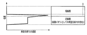
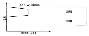
図3及び図4は、比較例としての構造を示している。
図3は、ポストアニール処理前の拡散イオンとしての典型元素TEの濃度分布であり、図4は、ポストアニール処理後の拡散イオンとしての典型元素TEの濃度分布である。3 and 4 show a structure as a comparative example.
FIG. 3 shows the concentration distribution of the typical element TE as diffusion ions before the post-annealing treatment, and FIG. 4 shows the concentration distribution of the typical element TE as diffusion ions after the post-annealing treatment.
比較例では、図3に示すように、ポストアニール処理前において、記録層内に拡散イオンとしての典型元素TEが均一に含まれており、電極層の、記録層に接する領域内、又は、記録層の、電極層に接する領域内に、拡散イオンとしての典型元素TEの濃度のピークを有しない。 In the comparative example, as shown in FIG. 3, the typical element TE as diffusion ions is uniformly contained in the recording layer before the post-annealing process, and the electrode layer is in the region in contact with the recording layer or the recording layer. There is no peak of the concentration of the typical element TE as diffusion ions in the region of the layer in contact with the electrode layer.
従って、図4に示すように、ポストアニール処理後においては、記録層内の拡散イオンとしての典型元素TEがほとんど全て電極層内に拡散してしまうため、上述のセット/リセット動作を安定的に行うことができない。 Therefore, as shown in FIG. 4, after the post-annealing process, almost all of the typical element TE as diffusion ions in the recording layer diffuses into the electrode layer, so that the above set / reset operation can be stably performed. I can't do it.
図2に示す第一の基本構造では、ポストアニール処理時に、電極層の、記録層に接する領域内、又は、記録層の、電極層に接する領域内に存在する拡散イオンとしての典型元素TEが電極層内に多少拡散する。しかし、それにより拡散イオンとしての典型元素TEの濃度プロファイルが大きく変わることはなく、ポストアニール処理後においても、電極層の、記録層に接する領域内、又は、記録層の、電極層に接する領域内に、拡散イオンとしての典型元素TEの濃度のピークを有する。 In the first basic structure shown in FIG. 2, the typical element TE as diffusion ions existing in the electrode layer in the region in contact with the recording layer or in the recording layer in the region in contact with the electrode layer is formed during the post-annealing process. Some diffusion in the electrode layer. However, this does not significantly change the concentration profile of the typical element TE as diffusion ions. Even after the post-annealing treatment, the electrode layer is in the region in contact with the recording layer or in the recording layer in the region in contact with the electrode layer. Inside, there is a peak of the concentration of the typical element TE as diffusion ions.
即ち、第一の基本構造では、比較例とは異なり、ポストアニール処理前後において、記録層内の拡散イオンとしての典型元素TEの濃度分布は変わらない。 That is, in the first basic structure, unlike the comparative example, the concentration distribution of the typical element TE as the diffusion ions in the recording layer does not change before and after the post-annealing process.
従って、既に述べたように、上述のセット/リセット動作を安定的に行うことが可能になる。 Therefore, as described above, the set / reset operation described above can be performed stably.
図5は、第二の基本構造を示している。
記録層は、拡散イオンとしての典型元素TEを含み、典型元素TEの移動により異なる電気抵抗率の2以上の状態をとる。記録層は、例えば、ZnMn2O4である。FIG. 5 shows a second basic structure.
The recording layer contains a typical element TE as diffusion ions, and takes two or more states having different electrical resistivity due to the movement of the typical element TE. The recording layer is, for example, ZnMn 2 O 4 .
電極層は、記録層の一端に配置され、記録層に電圧又は電流を与えるために設けられる。 The electrode layer is disposed at one end of the recording layer and is provided for applying a voltage or a current to the recording layer.
そして、記録層の、電極層に接する領域Xは、記録層のその他の領域よりも、高い濃度の拡散イオンとしての典型元素TEを含む。即ち、記録層の、電極層に接する領域Xは、記録層のその他の領域とは組成が異なる組成相違記録層となる。この電極層の、記録層に接する領域Xは、記録層内の元素の拡散を防止する拡散防止機能を有する。 The region X in contact with the electrode layer of the recording layer contains the typical element TE as a diffusion ion having a higher concentration than the other regions of the recording layer. That is, the region X of the recording layer that is in contact with the electrode layer is a different composition recording layer having a composition different from that of the other regions of the recording layer. The region X of the electrode layer in contact with the recording layer has a diffusion preventing function for preventing diffusion of elements in the recording layer.
この場合も、第一の基本構造と同様に、記録層/電極層を形成した後にポストアニール処理(熱処理)を行っても、記録層内の拡散イオンとしての典型元素TEが電極層に拡散せず、ポストアニール処理の前後において記録層内の拡散イオンとしての典型元素TEの濃度を一定に保つことができる。 In this case, as in the first basic structure, even if post-annealing (heat treatment) is performed after the recording layer / electrode layer is formed, the typical element TE as diffusion ions in the recording layer is diffused into the electrode layer. First, the concentration of the typical element TE as diffusion ions in the recording layer can be kept constant before and after the post-annealing process.
従って、上述のセット/リセット動作を安定的に行うことが可能になる。 Therefore, the above set / reset operation can be stably performed.
図6は、第三の基本構造を示している。
第三の基本構造が上述の第一及び第二の基本構造と異なる点は、記録層の一端及び他端にそれぞれ電極層が配置されている点にある。FIG. 6 shows a third basic structure.
The third basic structure is different from the first and second basic structures described above in that electrode layers are disposed at one end and the other end of the recording layer, respectively.
記録層は、拡散イオンとしての典型元素TEを含み、典型元素TEの移動により異なる電気抵抗率の2以上の状態をとる。記録層は、例えば、ZnMn2O4である。The recording layer contains a typical element TE as diffusion ions, and takes two or more states having different electrical resistivity due to the movement of the typical element TE. The recording layer is, for example, ZnMn 2 O 4 .
第一及び第二の電極層は、記録層を挟み込み、典型元素TEの移動のために記録層に電圧又は電流を与えるために設けられる。 The first and second electrode layers are provided to sandwich the recording layer and apply voltage or current to the recording layer for the movement of the typical element TE.
第一の電極層と記録層との界面付近における典型元素の濃度分布及び第二の電極層と記録層との界面付近における典型元素の濃度分布の少なくとも一つは、図2(第一の基本構造)又は図5(第二の基本構造)に示す濃度分布と同じに設定される。 At least one of the concentration distribution of the typical element in the vicinity of the interface between the first electrode layer and the recording layer and the concentration distribution of the typical element in the vicinity of the interface between the second electrode layer and the recording layer are shown in FIG. Structure) or the concentration distribution shown in FIG. 5 (second basic structure).
ここで、二つの界面の少なくとも一つに図2又は図5の濃度分布を適用したのは、電極を構成する材料によっては、記録層内の拡散イオンとしての典型元素が電極層内に拡散し難くなることもあるからである。 Here, the concentration distribution shown in FIG. 2 or 5 is applied to at least one of the two interfaces, depending on the material constituting the electrode, a typical element as a diffusion ion in the recording layer diffuses into the electrode layer. It can be difficult.
第一及び第二の電極層が同じ材料から構成され、典型元素が第一及び第二の電極層内に拡散する恐れがある場合には、当然に、二つの界面のそれぞれに図2又は図5の濃度分布を適用するのが好ましい。 If the first and second electrode layers are made of the same material and there is a risk that the typical element may diffuse into the first and second electrode layers, then naturally, the two interfaces are each shown in FIG. A concentration distribution of 5 is preferably applied.
4. 実施形態
次に、最良と思われるいくつかの実施形態について説明する。
以下では、本発明の例を、プローブ型固体メモリに適用した場合とクロスポイント型固体メモリに適用した場合の2つについて説明する。4). Embodiment
Next, some embodiments considered to be the best will be described.
Below, the example of this invention is demonstrated about the case where it applies to a probe type solid memory, and the case where it applies to a cross point type solid memory.
(1) プローブ型固体メモリ
A. 構造
図7及び図8は、本発明の例に係わるプローブ型固体メモリを示している。(1) Probe type solid-state memory
A. Structure
7 and 8 show a probe type solid state memory according to an example of the present invention.
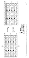
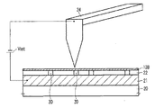
半導体基板20上には、電極層21が配置され、電極層21上には、データエリアとサーボエリアとを有する記録部22が配置される。記録部(記録媒体)22は、例えば、図2に示す記録層12から構成される。記録部22は、半導体基板20の中央部にベタに形成される。
An
サーボエリアは、半導体基板20の縁に沿って配置される。
The servo area is arranged along the edge of the
データエリア及びサーボエリアは、複数のブロックから構成される。データエリア上及びサーボエリア上には、複数のブロックに対応して複数のプローブ24が配置される。複数のプローブ24の各々は、先鋭化された形状を有する。
The data area and the servo area are composed of a plurality of blocks. On the data area and the servo area, a plurality of
複数のプローブ24は、プローブアレイを構成し、半導体基板23の一面側に形成される。複数のプローブ24は、MEMS技術を利用することにより、半導体基板23の一面側に容易に形成できる。
The plurality of
データエリア上のプローブ24の位置は、サーボエリアから読み出されるサーボバースト信号により制御される。具体的には、ドライバ27により、半導体基板20をX方向に往復運動させ、複数のプローブ24のY方向の位置制御を行うことにより、アクセス動作を実行する。
The position of the
尚、ブロックごとに記録媒体を独立に形成し、記録媒体がハードディスクのように円形で回転するような構造とし、複数のプローブ24の各々を、記録媒体の半径方向、例えば、X方向に移動させるようにしてもよい。
The recording medium is formed independently for each block, and the recording medium is configured to rotate in a circle like a hard disk, and each of the plurality of
複数のプローブ24は、それぞれ、記録/消去ヘッドとしての機能及び再生ヘッドとしての機能を有する。マルチプレクスドライバ25,26は、記録、再生及び消去時に、複数のプローブ24に対して所定の電圧を供給する。
Each of the plurality of
B. 記録/再生動作
図7及び図8のプローブ型固体メモリの記録/再生動作について説明する。B. Recording / playback operation
The recording / reproducing operation of the probe type solid-state memory shown in FIGS. 7 and 8 will be described.
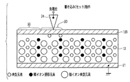
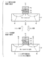
図9は、記録動作(セット動作)について示している。
記録部(記録媒体)22は、半導体チップ20上の電極層21上に形成される。記録部22は、保護層13Bにより覆われる。FIG. 9 shows the recording operation (set operation).
The recording unit (recording medium) 22 is formed on the
情報記録は、プローブ24の先端を保護層13Bの表面に接触させて、記録部(記録媒体)22の記録単位30に電圧パルスを印加し、記録部22の記録単位30内に電位勾配を発生させることにより行う。本例では、プローブ24の電位が電極層21の電位よりも相対的に低い状態を作る。電極層21を固定電位(例えば、接地電位)とすれば、プローブ24に負電位を与えればよい。
For information recording, the tip of the
電圧パルスは、例えば、電子発生源又はホットエレクトロン源を使用し、プローブ24から電極層21に向かって電子を放出することにより発生させてもよい。
The voltage pulse may be generated by emitting electrons from the
この時、例えば、図10に示すように、記録層12の記録単位30では、拡散イオンの一部がプローブ(陰極)24側に移動し、結晶内の拡散イオンが陰イオンに対して相対的に減少する。また、プローブ24側に移動した拡散イオンは、プローブ24から電子を受け取ってメタルとして析出する。
At this time, for example, as shown in FIG. 10, in the
記録層12の記録単位30では、陰イオンが過剰となり、結果的に、記録層12内に残された遷移元素イオンの価数を上昇させる。つまり、記録層12の記録単位30は、相変化によるキャリアの注入により電子伝導性を有するようになるため、情報記録(セット動作)が完了する。
In the
尚、情報記録のための電圧パルスは、プローブ24の電位が電極層21の電位よりも相対的に高い状態を作ることにより発生させることもできる。
The voltage pulse for recording information can be generated by creating a state in which the potential of the
本例のプローブ型固体メモリによれば、ハードディスクと同様に、記録媒体の記録単位30に情報記録を行うことができると共に、新規な記録材料を採用することにより、従来のハードディスクや半導体メモリよりも高記録密度が実現できる。
According to the probe type solid-state memory of this example, information can be recorded in the
図11は、再生動作について示している。
再生動作に関しては、電圧パルスを記録層12の記録単位30に流し、記録層12の記録単位30の抵抗値を検出することにより行う。但し、電圧パルスは、記録層12の記録単位30を構成する材料が相変化を起こさない程度の微小な値とする。FIG. 11 shows the reproduction operation.
The reproduction operation is performed by flowing a voltage pulse to the
例えば、センスアンプS/Aにより発生した読み出し電流をプローブ24から記録層12の記録単位30に流し、センスアンプS/Aにより記録単位30の抵抗値を測定する。既に説明した新材料を採用すると、高抵抗状態と低抵抗状態との抵抗の比は、103以上を確保できる。For example, the read current generated by the sense amplifier S / A is passed from the
尚、再生動作では、記録媒体上をプローブ24により走査(スキャン)することで、連続再生が可能となる。 In the reproducing operation, continuous reproduction is possible by scanning the recording medium with the probe 24 (scanning).
消去(リセット)動作に関しては、記録層12の記録単位30を大電流パルスによりジュール加熱して、記録層12の記録単位30における酸化還元反応を促進させることにより行う。或いは、セット時とは逆向きの電圧パルスを記録層12に印加することによっても行うことができる。
The erasure (reset) operation is performed by heating the
消去動作は、記録単位30ごとに行うこともできるし、複数の記録単位30又はブロック単位で行うこともできる。
The erasing operation can be performed for each
C. まとめ
このようなプローブ型固体メモリによれば、現在のハードディスクやフラッシュメモリよりも高記録密度及び低消費電力を実現できる。C. Summary
According to such a probe type solid-state memory, higher recording density and lower power consumption can be realized than current hard disks and flash memories.
(2) クロスポイント型固体メモリ
A. 構造
図12は、本発明の例に係わるクロスポイント型固体メモリを示している。(2) Cross-point type solid-state memory
A. Structure
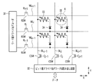
FIG. 12 shows a cross-point type solid-state memory according to an example of the present invention.
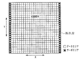
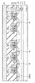
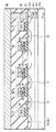
ワード線WLi−1,WLi,WLi+1は、X方向に延び、ビット線BLj−1,BLj,BLj+1は、Y方向に延びる。The word lines WL i−1 , WL i and WL i + 1 extend in the X direction, and the bit lines BL j−1 , BL j and BL j + 1 extend in the Y direction.
ワード線WLi−1,WLi,WLi+1の一端は、選択スイッチとしてのMOSトランジスタRSWを経由してワード線ドライバ&デコーダ31に接続され、ビット線BLj−1,BLj,BLj+1の一端は、選択スイッチとしてのMOSトランジスタCSWを経由してビット線ドライバ&デコーダ&読み出し回路32に接続される。One end of each of the word lines WL i−1 , WL i , WL i + 1 is connected to the word line driver &
MOSトランジスタRSWのゲートには、1本のワード線(ロウ)を選択するための選択信号Ri−1,Ri,Ri+1が入力され、MOSトランジスタCSWのゲートには、1本のビット線(カラム)を選択するための選択信号Cj−1,Cj,Cj+1が入力される。Selection signals R i−1 , R i and R i + 1 for selecting one word line (row) are input to the gate of the MOS transistor RSW, and one bit line is input to the gate of the MOS transistor CSW. Selection signals C j−1 , C j , C j + 1 for selecting (column) are input.
メモリセル33は、ワード線WLi−1,WLi,WLi+1とビット線BLj−1,BLj,BLj+1との交差部に配置される。いわゆるクロスポイント型セルアレイ構造である。The
メモリセル33には、記録/再生時における回り込み電流(sneak current)を防止するためのダイオード34が付加される。
The
図13は、図12のクロスポイント型固体メモリのメモリセルアレイ部の構造を示している。 FIG. 13 shows the structure of the memory cell array portion of the cross-point type solid-state memory shown in FIG.
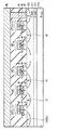
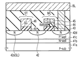
半導体チップ30上には、ワード線WLi−1,WLi,WLi+1とビット線BLj−1,BLj,BLj+1が配置され、これら配線の交差部にメモリセル33及びダイオード34が配置される。On the
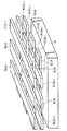
このようなクロスポイント型セルアレイ構造の特長は、メモリセル33に個別にMOSトランジスタを接続する必要がないため、高集積化に有利な点にある。例えば、図14及び図15に示すように、メモリセル33を積み重ねて、メモリセルアレイを3次元構造にすることも可能である。
The feature of such a cross-point cell array structure is that it is advantageous for high integration because it is not necessary to individually connect a MOS transistor to the
メモリセル33の構造例を説明する。
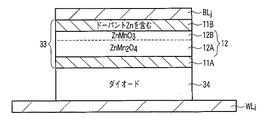
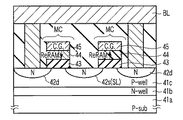
A structural example of the
図16は、メモリセルの第一例を示している。
ワード線WLi上にダイオード34が形成され、ダイオード34上にメモリセル33が形成される。メモリセル33は、電極層11A/記録層12/電極層11Bのスタック構造を有する。メモリセル33上にビット線BLjが形成される。FIG. 16 shows a first example of the memory cell.
A
電極層11Bは、添加物(ドーパント)として、記録層12内の拡散イオンとしての典型元素、即ち、亜鉛(Zn)を含む。また、その量(濃度)は、記録層12内の亜鉛(Zn)の量(濃度)よりも高い。
The
図17は、メモリセルの第二例を示している。
ワード線WLi上にダイオード34が形成され、ダイオード34上にメモリセル33が形成される。メモリセル33は、電極層11A/記録層12/電極層11Bのスタック構造を有する。さらに、記録層12は、電極層11Bに接する領域に存在する組成相違記録層12Bとその他の領域に存在する記録層本体12Aとから構成される。メモリセル33上にビット線BLjが形成される。FIG. 17 shows a second example of the memory cell.
A
記録層本体12Aと組成相違記録層12Bとは、同一の材料から構成され、両者の相違は、それらを構成する元素の組成比のみである。例えば、記録層本体12Aは、ZnMn2O4であり、組成相違記録層12Bは、ZnMnO3である。The recording layer
但し、組成相違記録層12B内の拡散イオンとしての典型元素、即ち、亜鉛(Zn)の量(濃度)は、記録層本体12A内の亜鉛(Zn)の量(濃度)よりも高い。
However, the amount (concentration) of the typical element as diffusion ions in the composition-
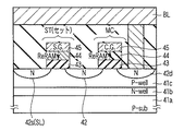
図18は、メモリセルの第三例を示している。
第三例は、第一例と第二例とを組み合わせた構造を有する。FIG. 18 shows a third example of the memory cell.
The third example has a structure in which the first example and the second example are combined.
ワード線WLi上にダイオード34が形成され、ダイオード34上にメモリセル33が形成される。メモリセル33は、電極層11A/記録層12/電極層11Bのスタック構造を有する。さらに、記録層12は、電極層11Bに接する領域に存在する組成相違記録層12Bとその他の領域に存在する記録層本体12Aとから構成される。メモリセル33上にビット線BLjが形成される。A
記録層本体12Aと組成相違記録層12Bとは、同一の材料から構成され、両者の相違は、それらを構成する元素の組成比のみである。例えば、記録層本体12Aは、ZnMn2O4であり、組成相違記録層12Bは、ZnMnO3である。The recording layer
但し、組成相違記録層12B内の拡散イオンとしての典型元素、即ち、亜鉛(Zn)の量(濃度)は、記録層本体12A内の亜鉛(Zn)の量(濃度)よりも高い。
However, the amount (concentration) of the typical element as diffusion ions in the composition-
また、電極層11Bは、添加物(ドーパント)として、記録層12内の拡散イオンとしての典型元素、即ち、亜鉛(Zn)を含む。また、その量(濃度)は、記録層本体12A内の亜鉛(Zn)の量(濃度)よりも高い。
The
図19は、メモリセルの第四例を示している。
第四例は、第一例の応用例であり、その特徴は、記録層12の両端に存在する電極層11A,11B内に、添加物(ドーパント)として、記録層12内の拡散イオンとしての典型元素を含ませた点にある。FIG. 19 shows a fourth example of the memory cell.
The fourth example is an application example of the first example, and its feature is that it is used as an additive (dopant) in the electrode layers 11A and 11B existing at both ends of the
ワード線WLi上にダイオード34が形成され、ダイオード34上にメモリセル33が形成される。メモリセル33は、電極層11A/記録層12/電極層11Bのスタック構造を有する。メモリセル33上にビット線BLjが形成される。A
電極層11A,11Bは、添加物(ドーパント)として、記録層12内の拡散イオンとしての典型元素、即ち、亜鉛(Zn)を含む。また、その量(濃度)は、記録層12内の亜鉛(Zn)の量(濃度)よりも高い。
The electrode layers 11A and 11B contain a typical element as diffusion ions in the
図20は、メモリセルの第五例を示している。
第五例は、第二例の応用例であり、その特徴は、記録層本体12Aの両端にそれぞれ組成相違記録層12A,12Bを配置した点にある。FIG. 20 shows a fifth example of the memory cell.
The fifth example is an application example of the second example, and is characterized in that the composition-
ワード線WLi上にダイオード34が形成され、ダイオード34上にメモリセル33が形成される。メモリセル33は、電極層11A/記録層12/電極層11Bのスタック構造を有する。さらに、記録層12は、電極層11Bに接する領域に存在する組成相違記録層12B、電極層11Aに接する領域に存在する組成相違記録層12C、及び、その他の領域に存在する記録層本体12Aから構成される。メモリセル33上にビット線BLjが形成される。A
記録層本体12Aと組成相違記録層12B,12Cとは、同一の材料から構成され、両者の相違は、それらを構成する元素の組成比のみである。例えば、記録層本体12Aは、ZnMn2O4であり、組成相違記録層12B,12Cは、ZnMnO3である。The recording layer
但し、組成相違記録層12B,12C内の拡散イオンとしての典型元素、即ち、亜鉛(Zn)の量(濃度)は、記録層本体12A内の亜鉛(Zn)の量(濃度)よりも高い。
However, the amount (concentration) of a typical element as diffusion ions in the composition-difference recording layers 12B and 12C, that is, zinc (Zn), is higher than the amount (concentration) of zinc (Zn) in the
また、二つの組成相違記録層12B,12Cの組成比は、異なっていてもよい。
Further, the composition ratio of the two composition
ところで、メモリセル33は、1ビット以上のデータを記憶する。また、ダイオード34は、ワード線WLiとメモリセル33との間ではなく、ビット線BLjとメモリセル33との間に配置してもよい。By the way, the
尚、ワード線WLiとダイオード34との間、及び、メモリセル33とビット線BLjとの間の少なくとも1つにバリアメタルを配置してもよい。A barrier metal may be disposed between at least one of the word line WL i and the
また、ダイオード34は、電圧の向きのみによってセット/リセット動作を行う場合には省略するのが好ましい。
The
B. 記録/再生動作
図12、図13及び図16を用いて記録/再生動作を説明する。
ここでは、点線Aで囲んだメモリセル33を選択し、これについて記録/再生動作を実行するものとする。B. Recording / playback operation
The recording / reproducing operation will be described with reference to FIGS.
Here, it is assumed that the
情報記録(セット動作)は、選択されたメモリセル33に電圧を印加し、そのメモリセル33内に電位勾配を発生させて電流パルスを流せばよいため、例えば、ワード線WLiの電位がビット線BLjの電位よりも相対的に低い状態を作る。ビット線BLjを固定電位(例えば、接地電位)とすれば、ワード線WLiに負電位を与えればよい。In the information recording (set operation), it is only necessary to apply a voltage to the selected
この時、点線Aで囲まれた選択されたメモリセル33の記録層12内では、拡散イオンの一部がワード線(陰極)WLi側に移動し、記録層12内の拡散イオンが陰イオンに対して相対的に減少する。また、ワード線WLi側に移動した拡散イオンは、ワード線WLiから電子を受け取ってメタルとして析出する。At this time, in the
点線Aで囲まれた選択されたメモリセル33の記録層12では、陰イオンが過剰となり、結果的に、記録層12内における遷移元素イオンの価数を上昇させる。つまり、点線Aで囲まれた選択されたメモリセル33は、相変化によるキャリアの注入により電子伝導性を有するようになるため、情報記録(セット動作)が完了する。
In the
尚、情報記録時には、非選択のワード線WLi−1,WLi+1及び非選択のビット線BLj−1,BLj+1については、全て同電位にバイアスしておくことが好ましい。During information recording, it is preferable that the non-selected word lines WL i−1 and WL i + 1 and the non-selected bit lines BL j−1 and BL j + 1 are all biased to the same potential.
また、情報記録前のスタンバイ時には、全てのワード線WLi−1,WLi,WLi+1及び全てのビット線BLj−1,BLj,BLj+1をプリチャージしておくことが好ましい。In standby before recording information, it is preferable to precharge all the word lines WL i−1 , WL i , WL i + 1 and all the bit lines BL j−1 , BL j , BL j + 1 .
また、情報記録のための電圧パルスは、ワード線WLiの電位がビット線BLjの電位よりも相対的に高い状態を作ることにより発生させてもよい。The voltage pulse for recording information may be generated by creating a state in which the potential of the word line WL i is relatively higher than the potential of the bit line BL j .
消去(リセット)動作は、選択されたメモリセル33に大電流パルスを流すことにより発生するジュール熱とその残留熱を利用するため、例えば、ワード線WLiの電位をビット線BLjの電位よりも相対的に高くする。ビット線BLjを固定電位(例えば、接地電位)とすれば、ワード線WLiに正の電位を与えればよい。Since the erase (reset) operation uses Joule heat generated by flowing a large current pulse to the selected
この時、点線Aで囲まれた選択されたメモリセル33の記録層12内に陽イオンの一部が移動する。このため、導電性酸化物層15内の陽イオン(遷移元素)の価数が増大し、記録層12内の陽イオン(遷移元素)の価数が減少する。
At this time, some of the cations move into the
その結果、メモリセル33は、低抵抗状態から高抵抗状態に変化し、リセット動作(消去)が完了する。
As a result, the
ここで、消去動作は、以下の方法により行うこともできる。 Here, the erasing operation can also be performed by the following method.
但し、この場合には、上述したように、図12、図13及び図16の半導体メモリからダイオード34を取り除くことが好ましい。
However, in this case, as described above, it is preferable to remove the
例えば、ワード線WLiの電位をビット線BLjの電位よりも相対的に低くする。ビット線BLjを固定電位(例えば、接地電位)とすれば、ワード線WLiに負の電位を与えればよい。For example, the potential of the word line WL i is made relatively lower than the potential of the bit line BL j . Bit lines BL j and a fixed potential (e.g., ground potential) if, a negative potential may be applied to the word line WL i.
この時、点線Aで囲まれた選択されたメモリセル33では、導電性酸化物層15内の陽イオンの一部が記録層12内に移動する。このため、導電性酸化物層15内の陽イオン(遷移元素)の価数が増大し、記録層12内の陽イオン(遷移元素)の価数が減少する。
At this time, in the selected
その結果、メモリセル33は、低抵抗状態から高抵抗状態に変化し、リセット動作(消去)が完了する。
As a result, the
尚、消去時にも、非選択のワード線WLi−1,WLi+1及び非選択のビット線BLj−1,BLj+1については、全て同電位にバイアスしておくことが好ましい。Even at the time of erasing, it is preferable that the unselected word lines WL i−1 and WL i + 1 and the unselected bit lines BL j−1 and BL j + 1 are all biased to the same potential.
また、消去前のスタンバイ時には、全てのワード線WLi−1,WLi,WLi+1及び全てのビット線BLj−1,BLj,BLj+1をプリチャージしておくことが好ましい。In standby before erasing, it is preferable to precharge all the word lines WL i−1 , WL i , WL i + 1 and all the bit lines BL j−1 , BL j , BL j + 1 .
読み出し動作は、電流パルスを点線Aで囲まれた選択されたメモリセル33に流し、そのメモリセル33の抵抗値を検出することにより行う。但し、電流パルスは、メモリセル33を構成する材料が抵抗変化を起こさない程度の微小な値とすることが必要である。
The read operation is performed by passing a current pulse through the selected
例えば、読み出し回路により発生した読み出し電流(電流パルス)をビット線BLjから点線Aで囲まれたメモリセル33に流し、読み出し回路によりそのメモリセル33の抵抗値を測定する。既に説明した新材料を採用すれば、セット/リセット状態の抵抗値の差は、103以上を確保できる。For example, read current generated by the reading circuit (current pulses) to the
C. まとめ
このようなクロスポイント型固体メモリによれば、現在のハードディスクやフラッシュメモリよりも高記録密度及び低消費電力を実現できる。C. Summary
According to such a cross-point type solid-state memory, higher recording density and lower power consumption can be realized than current hard disks and flash memories.
(3) その他
本実施形態では、プローブ型固体メモリとクロスポイント型固体メモリの2つについて説明したが、本発明の例で提案する材料及び原理を、現在のハードディスクやDVDなどの記録媒体に適用することも可能である。(3) Other
In this embodiment, the probe type solid-state memory and the cross-point type solid-state memory have been described. However, the material and principle proposed in the example of the present invention can be applied to a recording medium such as a current hard disk or DVD. It is.
5. フラッシュメモリへの適用
(1) 構造
本発明の例は、フラッシュメモリに適用することも可能である。5. Application to flash memory
(1) Structure
The example of the present invention can also be applied to a flash memory.
図21は、フラッシュメモリのメモリセルを示している。 FIG. 21 shows a memory cell of the flash memory.
フラッシュメモリのメモリセルは、MIS(metal-insulator-semiconductor)トランジスタから構成される。 The memory cell of the flash memory is composed of a MIS (metal-insulator-semiconductor) transistor.
半導体基板41の表面領域には、拡散層42が形成される。拡散層42の間のチャネル領域上には、ゲート絶縁層43が形成される。ゲート絶縁層43上には、本発明に係わる記録部(ReRAM: Resistive RAM)44が形成される。記録部44上には、コントロールゲート電極45が形成される。
A
半導体基板41は、ウェル領域でもよく、また、半導体基板41と拡散層42とは、互いに逆の導電型を有する。コントロールゲート電極45は、ワード線となり、例えば、導電性ポリシリコンから構成される。
The
記録部44は、例えば、図2の記録層から構成され、コントロールゲート電極45は、例えば、図2の電極層から構成される。
The
(2) 基本動作
図21を用いて基本動作について説明する。
セット(書き込み)動作は、コントロールゲート電極45に電位V1を与え、半導体基板41に電位V2を与えることにより実行する。(2) Basic operation
The basic operation will be described with reference to FIG.
The set (write) operation is performed by applying the potential V1 to the
電位V1,V2の差は、記録部44が相変化又は抵抗変化するのに十分な大きさであることが必要であるが、その向きについては、特に、限定されない。
The difference between the potentials V1 and V2 needs to be large enough for the
即ち、V1>V2及びV1<V2のいずれでもよい。 That is, either V1> V2 or V1 <V2 may be used.
例えば、初期状態(リセット状態)において、記録部44が絶縁体(抵抗大)であると仮定すると、実質的にゲート絶縁層43が厚くなったことになるため、メモリセル(MISトランジスタ)の閾値は、高くなる。
For example, assuming that the
この状態から電位V1,V2を与えて記録部44を導電体(抵抗小)に変化させると、実質的にゲート絶縁層43が薄くなったことになるため、メモリセル(MISトランジスタ)の閾値は、低くなる。
When the potentials V1 and V2 are applied from this state to change the
尚、電位V2は、半導体基板41に与えたが、これに代えて、メモリセルのチャネル領域に拡散層42から電位V2を転送するようにしてもよい。
Although the potential V2 is applied to the
リセット(消去)動作は、コントロールゲート電極45に電位V1’を与え、拡散層42の一方に電位V3を与え、拡散層42の他方に電位V4(<V3)を与えることにより実行する。
The reset (erase) operation is performed by applying the potential V1 'to the
電位V1’は、セット状態のメモリセルの閾値を越える値にする。 The potential V1 'is set to a value exceeding the threshold value of the memory cell in the set state.
この時、メモリセルは、オンになり、電子が拡散層42の他方から一方に向かって流れると共に、ホットエレクトロンが発生する。このホットエレクトロンは、ゲート絶縁層43を介して記録部44に注入されるため、記録部44の温度が上昇する。
At this time, the memory cell is turned on, electrons flow from one side of the
これにより、記録部44は、導電体(抵抗小)から絶縁体(抵抗大)に変化するため、実質的にゲート絶縁層43が厚くなったことになり、メモリセル(MISトランジスタ)の閾値は、高くなる。
As a result, since the
このように、フラッシュメモリと類似した原理により、メモリセルの閾値を変えることができるため、フラッシュメモリの技術を利用して、本発明の例に係る情報記録再生装置を実用化できる。 As described above, the threshold value of the memory cell can be changed based on a principle similar to that of the flash memory. Therefore, the information recording / reproducing apparatus according to the example of the present invention can be put into practical use by using the technology of the flash memory.
(3) NAND型フラッシュメモリ
図22は、NANDセルユニットの回路図を示している。図23は、本発明の例に係るNANDセルユニットの構造を示している。(3) NAND flash memory
FIG. 22 shows a circuit diagram of the NAND cell unit. FIG. 23 shows the structure of a NAND cell unit according to an example of the present invention.
P型半導体基板41a内には、N型ウェル領域41b及びP型ウェル領域41cが形成される。P型ウェル領域41c内に、本発明の例に係るNANDセルユニットが形成される。
An N-
NANDセルユニットは、直列接続される複数のメモリセルMCからなるNANDストリングと、その両端に1つずつ接続される合計2つのセレクトゲートトランジスタSTとから構成される。 The NAND cell unit is composed of a NAND string composed of a plurality of memory cells MC connected in series, and a total of two select gate transistors ST connected to the both ends one by one.
メモリセルMC及びセレクトゲートトランジスタSTは、同じ構造を有する。具体的には、これらは、N型拡散層42と、N型拡散層42の間のチャネル領域上のゲート絶縁層43と、ゲート絶縁層43上の記録部(ReRAM)44と、記録部44上のコントロールゲート電極45とから構成される。
The memory cell MC and the select gate transistor ST have the same structure. Specifically, these include an N-
メモリセルMCの記録部44の状態(絶縁体/導電体)は、上述の基本動作により変化させることが可能である。これに対し、セレクトゲートトランジスタSTの記録部44は、セット状態、即ち、導電体(抵抗小)に固定される。
The state (insulator / conductor) of the
セレクトゲートトランジスタSTの1つは、ソース線SLに接続され、他の1つは、ビット線BLに接続される。 One of the select gate transistors ST is connected to the source line SL, and the other one is connected to the bit line BL.
セット(書き込み)動作前には、NANDセルユニット内の全てのメモリセルは、リセット状態(抵抗大)になっているものとする。 It is assumed that all memory cells in the NAND cell unit are in a reset state (resistance is large) before the set (write) operation.
セット(書き込み)動作は、ソース線SL側のメモリセルMCからビット線BL側のメモリセルに向かって1つずつ順番に行われる。 The set (write) operation is sequentially performed one by one from the memory cell MC on the source line SL side to the memory cell on the bit line BL side.
選択されたワード線(コントロールゲート電極)WLに書き込み電位としてV1(プラス電位)を与え、非選択のワード線WLに転送電位(メモリセルMCがオンになる電位)としてVpassを与える。 V1 (plus potential) is applied to the selected word line (control gate electrode) WL as a write potential, and Vpass is applied to the unselected word line WL as a transfer potential (a potential at which the memory cell MC is turned on).
ソース線SL側のセレクトゲートトランジスタSTをオフ、ビット線BL側のセレクトゲートトランジスタSTをオンにし、ビット線BLから選択されたメモリセルMCのチャネル領域にプログラムデータを転送する。 The select gate transistor ST on the source line SL side is turned off, the select gate transistor ST on the bit line BL side is turned on, and program data is transferred from the bit line BL to the channel region of the selected memory cell MC.
例えば、プログラムデータが“1”のときは、選択されたメモリセルMCのチャネル領域に書き込み禁止電位(例えば、V1と同じ程度の電位)を転送し、選択されたメモリセルMCの記録部44の抵抗値が高い状態から低い状態に変化しないようにする。
For example, when the program data is “1”, a write inhibit potential (for example, the same potential as V1) is transferred to the channel region of the selected memory cell MC, and the
また、プログラムデータが“0”のときは、選択されたメモリセルMCのチャネル領域にV2(<V1)を転送し、選択されたメモリセルMCの記録部44の抵抗値を高い状態から低い状態に変化させる。
When the program data is “0”, V2 (<V1) is transferred to the channel region of the selected memory cell MC, and the resistance value of the
リセット(消去)動作では、例えば、全てのワード線(コントロールゲート電極)WLにV1’を与え、NANDセルユニット内の全てのメモリセルMCをオンにする。また、2つのセレクトゲートトランジスタSTをオンにし、ビット線BLにV3を与え、ソース線SLにV4(<V3)を与える。 In the reset (erase) operation, for example, V1 'is applied to all the word lines (control gate electrodes) WL, and all the memory cells MC in the NAND cell unit are turned on. Further, the two select gate transistors ST are turned on, V3 is applied to the bit line BL, and V4 (<V3) is applied to the source line SL.
この時、ホットエレクトロンがNANDセルユニット内の全てのメモリセルMCの記録部44に注入されるため、NANDセルユニット内の全てのメモリセルMCに対して一括してリセット動作が実行される。
At this time, since hot electrons are injected into the
読み出し動作は、選択されたワード線(コントロールゲート電極)WLに読み出し電位(プラス電位)を与え、非選択のワード線(コントロールゲート電極)WLには、メモリセルMCがデータ“0”、“1”によらず必ずオンになる電位を与える。 In the read operation, a read potential (plus potential) is applied to the selected word line (control gate electrode) WL, and the memory cell MC receives data “0”, “1” on the unselected word line (control gate electrode) WL. A potential to be turned on without fail is given.
また、2つのセレクトゲートトランジスタSTをオンにし、NANDストリングに読み出し電流を供給する。 Further, the two select gate transistors ST are turned on to supply a read current to the NAND string.
選択されたメモリセルMCは、読み出し電位が印加されると、それに記憶されたデータの値に応じてオン又はオフになるため、例えば、読み出し電流の変化を検出することにより、データを読み出すことができる。 When a read potential is applied to the selected memory cell MC, the selected memory cell MC is turned on or off according to the value of the data stored therein. For example, data can be read by detecting a change in the read current. it can.
尚、図23の構造では、セレクトゲートトランジスタSTは、メモリセルMCと同じ構造を有しているが、例えば、図24に示すように、セレクトゲートトランジスタSTについては、記録部(記録層)を形成せずに、通常のMISトランジスタとすることも可能である。 In the structure of FIG. 23, the select gate transistor ST has the same structure as the memory cell MC. For example, as shown in FIG. 24, the select gate transistor ST has a recording portion (recording layer). A normal MIS transistor may be used without forming it.
図25は、NAND型フラッシュメモリの変形例である。 FIG. 25 shows a modification of the NAND flash memory.
この変形例は、NANDストリングを構成する複数のメモリセルMCのゲート絶縁層がP型半導体層47に置き換えられている点に特徴を有する。
This modification is characterized in that the gate insulating layers of the plurality of memory cells MC constituting the NAND string are replaced with a P-
高集積化が進み、メモリセルMCが微細化されると、電圧を与えていない状態で、P型半導体層47は、空乏層で満たされることになる。
When the high integration progresses and the memory cell MC is miniaturized, the P-
セット(書き込み)時には、選択されたメモリセルMCのコントロールゲート電極45にプラスの書き込み電位(例えば、3.5V)を与え、かつ、非選択のメモリセルMCのコントロールゲート電極45にプラスの転送電位(例えば、1V)を与える。
At the time of setting (writing), a positive write potential (for example, 3.5 V) is applied to the
この時、NANDストリング内の複数のメモリセルMCのP型ウェル領域41cの表面がP型からN型に反転し、チャネルが形成される。
At this time, the surface of the P-
そこで、上述したように、ビット線BL側のセレクトゲートトランジスタSTをオンにし、ビット線BLから選択されたメモリセルMCのチャネル領域にプログラムデータ“0”を転送すれば、セット動作を行うことができる。 Therefore, as described above, the set operation can be performed by turning on the select gate transistor ST on the bit line BL side and transferring the program data “0” from the bit line BL to the channel region of the selected memory cell MC. it can.
リセット(消去)は、例えば、全てのコントロールゲート電極45にマイナスの消去電位(例えば、-3.5V)を与え、P型ウェル領域41c及びP型半導体層47に接地電位(0V)を与えれば、NANDストリングを構成する全てのメモリセルMCに対して一括して行うことができる。
For example, reset (erase) is performed by applying a negative erase potential (for example, −3.5 V) to all the
読み出し時には、選択されたメモリセルMCのコントロールゲート電極45にプラスの読み出し電位(例えば、0.5V)を与え、かつ、非選択のメモリセルMCのコントロールゲート電極45に、メモリセルMCがデータ“0”、“1”によらず必ずオンになる転送電位(例えば、1V)を与える。
At the time of reading, a positive read potential (for example, 0.5 V) is applied to the
但し、“1”状態のメモリセルMCの閾値電圧Vth”1”は、0V < Vth”1” < 0.5Vの範囲内にあるものとし、“0”状態のメモリセルMCの閾値電圧Vth”0”は、0.5V < Vth”0” < 1Vの範囲内にあるものとする。 However, the threshold voltage Vth ”1” of the memory cell MC in the “1” state is in the range of 0V <Vth ”1” <0.5V, and the threshold voltage Vth ”0 of the memory cell MC in the“ 0 ”state "" Is assumed to be in the range of 0.5V <Vth "0" <1V.
また、2つのセレクトゲートトランジスタSTをオンにし、NANDストリングに読み出し電流を供給する。 Further, the two select gate transistors ST are turned on to supply a read current to the NAND string.
このような状態にすれば、選択されたメモリセルMCに記憶されたデータの値に応じてNANDストリングに流れる電流量が変わるため、この変化を検出することにより、データを読み出すことができる。 In such a state, since the amount of current flowing through the NAND string changes according to the value of the data stored in the selected memory cell MC, data can be read by detecting this change.
尚、この変形例においては、P型半導体層47のホールドープ量がP型ウェル領域41cのそれよりも多く、かつ、P型半導体層47のフェルミレベルがP型ウェル領域41cのそれよりも0.5V程度深くなっていることが好ましい。
In this modification, the hole doping amount of the P-
これは、コントロールゲート電極45にプラスの電位を与えたときに、N型拡散層42間のP型ウェル領域41cの表面部分からP型からN型への反転が開始し、チャネルが形成されるようにするためである。
This is because when a positive potential is applied to the
このようにすることで、例えば、書き込み時には、非選択のメモリセルMCのチャネルは、P型ウェル領域41cとP型半導体層47の界面のみに形成され、読み出し時には、NANDストリング内の複数のメモリセルMCのチャネルは、P型ウェル領域41cとP型半導体層47の界面のみに形成される。
Thus, for example, at the time of writing, the channel of the non-selected memory cell MC is formed only at the interface between the P-
つまり、メモリセルMCの記録部44が導電体(セット状態)であっても、拡散層42とコントロールゲート電極45とが短絡することはない。
That is, even if the
(4) NOR型フラッシュメモリ
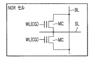
図26は、NORセルユニットの回路図を示している。図27は、本発明の例に係るNORセルユニットの構造を示している。(4) NOR flash memory
FIG. 26 shows a circuit diagram of the NOR cell unit. FIG. 27 shows the structure of a NOR cell unit according to an example of the present invention.
P型半導体基板41a内には、N型ウェル領域41b及びP型ウェル領域41cが形成される。P型ウェル領域41c内に、本発明の例に係るNORセルが形成される。
An N-
NORセルは、ビット線BLとソース線SLとの間に接続される1つのメモリセル(MISトランジスタ)MCから構成される。 The NOR cell is composed of one memory cell (MIS transistor) MC connected between the bit line BL and the source line SL.
メモリセルMCは、N型拡散層42と、N型拡散層42の間のチャネル領域上のゲート絶縁層43と、ゲート絶縁層43上の記録部(ReRAM)44と、記録部44上のコントロールゲート電極45とから構成される。
The memory cell MC includes an N-
メモリセルMCの記録部44の状態(絶縁体/導電体)は、上述の基本動作により変化させることが可能である。
The state (insulator / conductor) of the
(5) 2トラ型フラッシュメモリ
図28は、2トラセルユニットの回路図を示している。図29は、本発明の例に係る2トラセルユニットの構造を示している。(5) Two-tra type flash memory
FIG. 28 shows a circuit diagram of a 2-tracell unit. FIG. 29 shows the structure of a two-tracell unit according to an example of the present invention.
2トラセルユニットは、NANDセルユニットの特徴とNORセルの特徴とを併せ持った新たなセル構造として最近開発されたものである。 The 2-tra cell unit has been recently developed as a new cell structure that combines the characteristics of a NAND cell unit and the characteristics of a NOR cell.
P型半導体基板41a内には、N型ウェル領域41b及びP型ウェル領域41cが形成される。P型ウェル領域41c内に、本発明の例に係る2トラセルユニットが形成される。
An N-
2トラセルユニットは、直列接続される1つのメモリセルMCと1つのセレクトゲートトランジスタSTとから構成される。 The two tracell unit is composed of one memory cell MC and one select gate transistor ST connected in series.
メモリセルMC及びセレクトゲートトランジスタSTは、同じ構造を有する。具体的には、これらは、N型拡散層42と、N型拡散層42の間のチャネル領域上のゲート絶縁層43と、ゲート絶縁層43上の記録部(ReRAM)44と、記録部44上のコントロールゲート電極45とから構成される。
The memory cell MC and the select gate transistor ST have the same structure. Specifically, these include an N-
メモリセルMCの記録部44の状態(絶縁体/導電体)は、上述の基本動作により変化させることが可能である。これに対し、セレクトゲートトランジスタSTの記録部44は、セット状態、即ち、導電体(抵抗小)に固定される。
The state (insulator / conductor) of the
セレクトゲートトランジスタSTは、ソース線SLに接続され、メモリセルMCは、ビット線BLに接続される。 Select gate transistor ST is connected to source line SL, and memory cell MC is connected to bit line BL.
メモリセルMCの記録部44の状態(絶縁体/導電体)は、上述の基本動作により変化させることが可能である。
The state (insulator / conductor) of the
図29の構造では、セレクトゲートトランジスタSTは、メモリセルMCと同じ構造を有しているが、例えば、図30に示すように、セレクトゲートトランジスタSTについては、記録部(記録層)を形成せずに、通常のMISトランジスタとすることも可能である。 In the structure of FIG. 29, the select gate transistor ST has the same structure as the memory cell MC. For example, as shown in FIG. 30, the select gate transistor ST is not formed with a recording portion (recording layer). Alternatively, a normal MIS transistor can be used.
6. むすび
本発明によれば、高記録密度及び低消費電力の不揮発性の情報記録再生装置を実現できる。6). Conclusion
According to the present invention, a nonvolatile information recording / reproducing apparatus with high recording density and low power consumption can be realized.
本発明の例は、上述の実施形態に限定されるものではなく、その要旨を逸脱しない範囲で、各構成要素を変形して具体化できる。また、上述の実施形態に開示されている複数の構成要素の適宜な組み合せにより種々の発明を構成できる。例えば、上述の実施形態に開示される全構成要素から幾つかの構成要素を削除してもよいし、異なる実施形態の構成要素を適宜組み合わせてもよい。 The example of the present invention is not limited to the above-described embodiment, and can be embodied by modifying each component without departing from the gist thereof. Various inventions can be configured by appropriately combining a plurality of constituent elements disclosed in the above-described embodiments. For example, some constituent elements may be deleted from all the constituent elements disclosed in the above-described embodiments, or constituent elements of different embodiments may be appropriately combined.
本発明の例に関わる情報記録再生装置よれば、極めて単純な仕組みであるにもかかわらず、従来技術では到達することのできない記録密度による情報記録を可能とすると同時に高速動作を実現することが可能になる。従って、本発明の例は、現在の不揮発性メモリの記録密度の壁を打ち破る次世代技術として産業上のメリットは多大である。 According to the information recording / reproducing apparatus according to the example of the present invention, it is possible to perform information recording at a recording density that cannot be achieved by the conventional technology, but at the same time, it is possible to realize high-speed operation even though it is an extremely simple mechanism. become. Therefore, the example of the present invention has a great industrial advantage as a next generation technology that breaks down the recording density barrier of the current nonvolatile memory.
Claims (9)
前記電極層は、前記記録層に接する第1領域を有し、前記記録層は、前記電極層に接する第2領域を有し、前記第1及び第2領域は、対向し、前記第1領域は、前記第2領域内の前記典型元素の濃度よりも高い濃度の前記典型元素を添加物として含んでいる
ことを特徴とする情報記録再生装置。A recording layer that includes a diode and a laminated structure together with the diode, includes at least one kind of typical element and transition element, and records two states of different electrical resistivity due to movement of the typical element; and the recording layer And an electrode layer for applying a voltage or current to the recording layer,
The electrode layer has a first region in contact with the recording layer, the recording layer has a second region in contact with the electrode layer, the first and second regions face each other, and the first region The information recording / reproducing apparatus includes the typical element having a concentration higher than the concentration of the typical element in the second region as an additive.
前記記録層は、前記電極層に接する第1領域と、前記第1領域以外の第2領域とを有し、前記第1及び第2領域は、組成が相違しており、前記第1領域は、前記第2領域内の前記典型元素の濃度よりも高い濃度の前記典型元素を添加物として含んでいる
ことを特徴とする情報記録再生装置。 A diode, a stacked structure together with the diode, including at least one kind of typical element and transition element, and two states having different electrical resistivity recorded by movement of the typical element; and An electrode layer disposed at one end and applying voltage or current to the recording layer;
The recording layer has a first region in contact with the electrode layer and a second region other than the first region, and the first and second regions have different compositions, and the first region is An information recording / reproducing apparatus comprising the typical element in a concentration higher than the concentration of the typical element in the second region as an additive .
化学式: AxMyX4(0.1≦x≦2.2、1.5≦y≦2)
但し、Aは、Zn、Cd、Hgのグループから選択される典型元素、Mは、Cu、Mo、W、Mn、Tc、Re、Feのグループから選択される遷移元素、Xは、O、Nのグループから選択される元素である。
で表される材料を含むことを特徴とする請求項1又は2に記載の情報記録再生装置。The recording layer is
Formula: A x M y X 4 ( 0.1 ≦ x ≦ 2.2,1.5 ≦ y ≦ 2)
However, A is a typical element selected from the group of Zn, Cd, and Hg, M is a transition element selected from the group of Cu, Mo, W, Mn, Tc, Re, and Fe, and X is O, N Element selected from the group of
Information recording and reproducing apparatus according in to contain represented material to claim 1 or 2, characterized in.
Applications Claiming Priority (1)
| Application Number | Priority Date | Filing Date | Title |
|---|---|---|---|
| PCT/JP2008/056499 WO2009122572A1 (en) | 2008-04-01 | 2008-04-01 | Information recording and replaying apparatus |
Publications (2)
| Publication Number | Publication Date |
|---|---|
| JPWO2009122572A1 JPWO2009122572A1 (en) | 2011-07-28 |
| JP4792125B2 true JP4792125B2 (en) | 2011-10-12 |
Family
ID=41134992
Family Applications (1)
| Application Number | Title | Priority Date | Filing Date |
|---|---|---|---|
| JP2010505229A Expired - Fee Related JP4792125B2 (en) | 2008-04-01 | 2008-04-01 | Information recording / reproducing device |
Country Status (4)
| Country | Link |
|---|---|
| US (1) | US8431920B2 (en) |
| JP (1) | JP4792125B2 (en) |
| TW (1) | TWI406407B (en) |
| WO (1) | WO2009122572A1 (en) |
Families Citing this family (5)
| Publication number | Priority date | Publication date | Assignee | Title |
|---|---|---|---|---|
| US9070876B2 (en) * | 2011-03-18 | 2015-06-30 | Nec Corporation | Variable resistance element and semiconductor storage device |
| US8711601B2 (en) * | 2011-12-28 | 2014-04-29 | Industrial Technology Research Institute | Resistive random access memory cell and resistive random access memory module |
| JP5798052B2 (en) * | 2012-01-31 | 2015-10-21 | 株式会社東芝 | Storage device |
| US8664632B2 (en) * | 2012-01-31 | 2014-03-04 | Kabushiki Kaisha Toshiba | Memory device |
| TWI572074B (en) * | 2015-02-04 | 2017-02-21 | 力晶科技股份有限公司 | Resistive random access memory and method for manufacturing the same |
Citations (2)
| Publication number | Priority date | Publication date | Assignee | Title |
|---|---|---|---|---|
| WO2005101420A1 (en) * | 2004-04-16 | 2005-10-27 | Matsushita Electric Industrial Co. Ltd. | Thin film memory device having a variable resistance |
| JP2006140412A (en) * | 2004-11-15 | 2006-06-01 | Sony Corp | Storage element and storage device |
Family Cites Families (6)
| Publication number | Priority date | Publication date | Assignee | Title |
|---|---|---|---|---|
| US5825046A (en) * | 1996-10-28 | 1998-10-20 | Energy Conversion Devices, Inc. | Composite memory material comprising a mixture of phase-change memory material and dielectric material |
| JP3974756B2 (en) * | 2001-06-05 | 2007-09-12 | 株式会社日本触媒 | Method for producing metal oxide particles |
| KR100906056B1 (en) * | 2002-03-19 | 2009-07-03 | 파나소닉 주식회사 | Information recording medium and its manufacturing method |
| US7719875B2 (en) * | 2003-03-18 | 2010-05-18 | Kabushiki Kaisha Toshiba | Resistance change memory device |
| US7326950B2 (en) * | 2004-07-19 | 2008-02-05 | Micron Technology, Inc. | Memory device with switching glass layer |
| US7733684B2 (en) * | 2005-12-13 | 2010-06-08 | Kabushiki Kaisha Toshiba | Data read/write device |
-
2008
- 2008-04-01 WO PCT/JP2008/056499 patent/WO2009122572A1/en not_active Ceased
- 2008-04-01 JP JP2010505229A patent/JP4792125B2/en not_active Expired - Fee Related
-
2009
- 2009-03-30 TW TW098110468A patent/TWI406407B/en not_active IP Right Cessation
-
2010
- 2010-09-17 US US12/884,880 patent/US8431920B2/en not_active Expired - Fee Related
Patent Citations (2)
| Publication number | Priority date | Publication date | Assignee | Title |
|---|---|---|---|---|
| WO2005101420A1 (en) * | 2004-04-16 | 2005-10-27 | Matsushita Electric Industrial Co. Ltd. | Thin film memory device having a variable resistance |
| JP2006140412A (en) * | 2004-11-15 | 2006-06-01 | Sony Corp | Storage element and storage device |
Also Published As
| Publication number | Publication date |
|---|---|
| JPWO2009122572A1 (en) | 2011-07-28 |
| US8431920B2 (en) | 2013-04-30 |
| US20110062407A1 (en) | 2011-03-17 |
| TWI406407B (en) | 2013-08-21 |
| WO2009122572A1 (en) | 2009-10-08 |
| TW201003909A (en) | 2010-01-16 |
Similar Documents
| Publication | Publication Date | Title |
|---|---|---|
| JP5351144B2 (en) | Information recording / reproducing device | |
| JP4792107B2 (en) | Information recording / reproducing device | |
| JP5216847B2 (en) | Information recording / reproducing device | |
| JP4792008B2 (en) | Information recording / reproducing device | |
| JP4792007B2 (en) | Information recording / reproducing device | |
| JP4792009B2 (en) | Information recording / reproducing device | |
| JP4792006B2 (en) | Information recording / reproducing device | |
| JP4908555B2 (en) | Information recording / reproducing device | |
| JPWO2009122569A1 (en) | Information recording / reproducing device | |
| KR20070062937A (en) | Data read / write device | |
| JP4791948B2 (en) | Information recording / reproducing device | |
| JP4792125B2 (en) | Information recording / reproducing device | |
| JP2008251108A (en) | Information recording / reproducing device | |
| JP4792108B2 (en) | Information recording / reproducing device | |
| JP4977158B2 (en) | Information recording / reproducing device | |
| JPWO2009116139A1 (en) | Information recording / reproducing device | |
| WO2009122571A1 (en) | Information recording/reproducing device | |
| JP2008276904A (en) | Information recording / reproducing device | |
| JP2012138512A (en) | Information recording/reproducing apparatus | |
| JP2008251107A (en) | Information recording / reproducing device | |
| JP2008251126A (en) | Information recording / reproducing device |
Legal Events
| Date | Code | Title | Description |
|---|---|---|---|
| A131 | Notification of reasons for refusal |
Free format text: JAPANESE INTERMEDIATE CODE: A131 Effective date: 20110308 |
|
| A521 | Request for written amendment filed |
Free format text: JAPANESE INTERMEDIATE CODE: A523 Effective date: 20110509 |
|
| TRDD | Decision of grant or rejection written | ||
| A01 | Written decision to grant a patent or to grant a registration (utility model) |
Free format text: JAPANESE INTERMEDIATE CODE: A01 Effective date: 20110628 |
|
| A01 | Written decision to grant a patent or to grant a registration (utility model) |
Free format text: JAPANESE INTERMEDIATE CODE: A01 |
|
| A61 | First payment of annual fees (during grant procedure) |
Free format text: JAPANESE INTERMEDIATE CODE: A61 Effective date: 20110722 |
|
| FPAY | Renewal fee payment (event date is renewal date of database) |
Free format text: PAYMENT UNTIL: 20140729 Year of fee payment: 3 |
|
| LAPS | Cancellation because of no payment of annual fees |