JP4779305B2 - Multiplier circuit, oscillation circuit, and wireless communication device - Google Patents
Multiplier circuit, oscillation circuit, and wireless communication device Download PDFInfo
- Publication number
- JP4779305B2 JP4779305B2 JP2004134279A JP2004134279A JP4779305B2 JP 4779305 B2 JP4779305 B2 JP 4779305B2 JP 2004134279 A JP2004134279 A JP 2004134279A JP 2004134279 A JP2004134279 A JP 2004134279A JP 4779305 B2 JP4779305 B2 JP 4779305B2
- Authority
- JP
- Japan
- Prior art keywords
- output
- terminal
- signal
- terminals
- circuit
- Prior art date
- Legal status (The legal status is an assumption and is not a legal conclusion. Google has not performed a legal analysis and makes no representation as to the accuracy of the status listed.)
- Expired - Fee Related
Links
Images


Description
本発明は、入力信号の周波数を逓倍する逓倍回路、この逓倍回路を用いた発振回路、並びに無線通信装置に関するものである。 The present invention relates to a multiplier circuit that multiplies the frequency of an input signal, an oscillation circuit using the multiplier circuit, and a wireless communication apparatus.
入力信号の2倍の周波数の信号を生成する2逓倍回路が、たとえば特許文献1に記載されている。
For example,
図10は、特許文献1に記載された2逓倍回路の基本構成を示す回路図である。
この2逓倍回路1は、図10に示すように、絶縁ゲート型電界効果トランジスタであるMOSトランジスタQ1,Q2、負荷抵抗素子R1、キャパシタC1、差動入力端子TIN,TINX、および出力端子TOUTを有している。
FIG. 10 is a circuit diagram showing a basic configuration of the double circuit described in
As shown in FIG. 10, the
MOSトランジスタQ1のゲートが信号INの入力端子TINに接続され、MOSトランジスタQ2のゲートが信号INXの入力端子TINXに接続されている。
MOSトランジスタQ1およびQ2のソースが接地され、ドレイン同士が接続され、ドレイン同士の接続点が抵抗素子R1の一端に接続され、抵抗素子の他端が電源電位VCCに接続されている。そして、MOSトランジスタQ1およびQ2のドレイン同士の接続点と抵抗素子R1の一端との接続点がキャパシタC1の第1電極に接続され、キャパシタC1の第2電極が出力端子TOUTに接続されている。
The gate of the MOS transistor Q1 is connected to the input terminal TIN for the signal IN, and the gate of the MOS transistor Q2 is connected to the input terminal TINX for the signal INX.
The sources of the MOS transistors Q1 and Q2 are grounded, the drains are connected, the connection point between the drains is connected to one end of the resistance element R1, and the other end of the resistance element is connected to the power supply potential VCC. The connection point between the drains of the MOS transistors Q1 and Q2 and one end of the resistor element R1 is connected to the first electrode of the capacitor C1, and the second electrode of the capacitor C1 is connected to the output terminal TOUT.
このような構成を有する2逓倍回路1において、差動の入力信号IN,INXが入力されると、これらの入力信号IN,INXの電圧がMOSトランジスタQ1,Q2のしきい値電圧より大きいときに負荷に電流が流れることで半整流を行い、入力信号の周波数に対して2倍の周波数の出力を得る。
一般に、2逓倍回路は、電圧制御発振器(VCO:Voltage Controlled Oscillator)か増幅器の出力側に接続して用いられる。
ところが、2逓倍回路の出力レベルは、負荷に流れる電流に依存する。この電流は前段に接続されたVCOや増幅器の振幅や2逓倍回路を構成するデバイスの特性によって変化する。
このため、従来の2逓倍回路では出力レベルを一定に保つことが困難という不利益があった。
In general, the double circuit is used by being connected to a voltage controlled oscillator (VCO) or an output side of an amplifier.
However, the output level of the doubler circuit depends on the current flowing through the load. This current varies depending on the VCO connected in the previous stage, the amplitude of the amplifier, and the characteristics of the devices constituting the double circuit.
For this reason, the conventional double circuit has the disadvantage that it is difficult to keep the output level constant.
本発明は、かかる事情に鑑みてなされたものであり、その目的は、出力レベルを一定に保つことが可能な逓倍回路、この逓倍回路を用いた発振回路、並びに無線通信装置を提供することにある。 The present invention has been made in view of such circumstances, and an object of the present invention is to provide a multiplication circuit capable of keeping the output level constant, an oscillation circuit using the multiplication circuit, and a wireless communication device. is there.
上記目的を達成するため、本発明の第1の観点は、制御信号に応じて差動発振出力信号の振幅を制御可能な信号出力回路による差動発振出力信号の周波数を逓倍した信号を生成する逓倍回路であって、上記信号出力回路による差動発振出力信号の周波数を逓倍した信号を生成して出力するコア回路と、上記信号出力回路による差動発振出力信号を受けて上記コア回路の出力信号と等価なレベルの信号を生成するモニタ回路と、上記モニタ回路の信号出力レベルに基づいて、上記コア回路の出力信号のレベルが一定となるように上記制御信号を生成して上記信号出力回路に出力する制御信号生成手段と、を有し、上記コア回路は、制御端子並びに入出力用の第1の端子および第2の端子を有する第1から第6のトランジスタと、第1電源に接続された第1の負荷素子と、第2電源に接続された第1の電流源と、を含み、上記第1および第2のトランジスタの第1の端子同士が接続され、その接続点が上記第1の負荷素子に接続され、並びに、第2の端子同士が接続され、その接続点が上記第5のトランジスタの第1の端子に接続され、上記第3および第4のトランジスタの第1の端子同士が接続され、その接続点が出力負荷に接続され、並びに、第2の端子同士が接続され、その接続点が上記6のトランジスタの第1の端子に接続され、上記第5および第6のトランジスタの第2の端子同士が接続され、その接続点が上記第1の電流源に接続され、上記第1、第4および第5のトランジスタの制御端子が上記差動発振出力信号のうちの一方の出力信号の供給ラインに接続され、上記第2、第3および第6のトランジスタの制御端子が上記差動発振出力信号のうちの他方の出力信号の供給ラインに接続され、上記モニタ回路は、制御端子並びに入出力用の第1の端子および第2の端子を有する第7から第12のトランジスタと、第1電源に接続された第2の負荷素子と、第2電源に接続された第2の電流源と、を含み、上記第7および第8のトランジスタの第1の端子同士が接続され、その接続点が上記第2の負荷素子に接続され、並びに、第2の端子同士が接続され、その接続点が上記第11のトランジスタの第1の端子に接続され、上記第9および第10のトランジスタの第1の端子同士が接続され、その接続点が出力端子に接続され、当該出力端子が上記制御信号生成手段に接続され、並びに、第2の端子同士が接続され、その接続点が上記第12のトランジスタの第1の端子に接続され、上記第11および第12のトランジスタの第2の端子同士が接続され、その接続点が上記第2の電流源に接続され、上記第7、第10および第11のトランジスタの制御端子が上記差動発振出力信号のうちの一方の出力信号の供給ラインに接続され、上記第8、第9および第12のトランジスタの制御端子が上記差動発振出力信号のうちの他方の出力信号の供給ラインに接続され、上記制御信号生成手段は、定電流源と、低インピーダンス入力端子が上記モニタ回路の出力端子に接続され、高インピーダンス出力端子が上記定電流源に接続されたカンレトミラー回路と、を含み、上記定電流源と上記カンレトミラー回路の高インピーダンス出力端子との接続点により上記制御信号を出力する。 In order to achieve the above object, a first aspect of the present invention generates a signal obtained by multiplying the frequency of a differential oscillation output signal by a signal output circuit capable of controlling the amplitude of the differential oscillation output signal in accordance with a control signal. A multiplier circuit for generating and outputting a signal obtained by multiplying the frequency of the differential oscillation output signal by the signal output circuit; and an output of the core circuit upon receiving the differential oscillation output signal by the signal output circuit A monitor circuit that generates a signal having a level equivalent to the signal; and the signal output circuit that generates the control signal based on the signal output level of the monitor circuit so that the level of the output signal of the core circuit is constant. And a control signal generating means for outputting to the control circuit, wherein the core circuit is connected to the first power source and the first to sixth transistors having the control terminal, the first terminal for input / output, and the second terminal. A first current source connected to a second power source, the first terminals of the first and second transistors are connected to each other, and the connection point is the first current source. Connected to the first load element, the second terminals are connected to each other, the connection point is connected to the first terminal of the fifth transistor, and the first terminals of the third and fourth transistors Are connected to each other, the connection point is connected to the output load, the second terminals are connected to each other, the connection point is connected to the first terminal of the transistor of the sixth, and the fifth and sixth The second terminals of the transistors are connected to each other, the connection point is connected to the first current source, and the control terminal of the first, fourth, and fifth transistors is one of the differential oscillation output signals. Connected to the output signal supply line of the The control terminals of the third and sixth transistors are connected to a supply line for the other output signal of the differential oscillation output signals, and the monitor circuit includes a control terminal, a first terminal for input / output, and a first terminal. 7th to 12th transistors having two terminals, a second load element connected to the first power supply, and a second current source connected to the second power supply, The first terminals of the eight transistors are connected, the connection point is connected to the second load element, and the second terminals are connected, and the connection point is the first of the eleventh transistor. The first terminals of the ninth and tenth transistors are connected to each other, the connection point is connected to the output terminal, the output terminal is connected to the control signal generating means, and the first The two terminals are connected The connection point is connected to the first terminal of the twelfth transistor, the second terminals of the eleventh and twelfth transistors are connected to each other, and the connection point is connected to the second current source. The control terminals of the seventh, tenth and eleventh transistors are connected to the supply line of one of the differential oscillation output signals, and the control terminals of the eighth, ninth and twelfth transistors. Is connected to the supply line of the other output signal of the differential oscillation output signal, and the control signal generating means has a constant current source, a low impedance input terminal connected to the output terminal of the monitor circuit, and a high impedance A current mirror circuit having an output terminal connected to the constant current source, and the control point is controlled by a connection point between the constant current source and the high impedance output terminal of the current mirror circuit. And it outputs the signal.
好適には、上記コア回路と上記モニタ回路は、出力端子が負荷に接続され、上記信号出力回路による信号が制御端子に供給され、当該出力端子から逓倍した信号を出力するトランジスタを含み、上記制御信号生成手段は、上記モニタ回路に流れる電流を検知して検知結果に応じて上記制御信号を生成する。 Preferably, the core circuit and the monitor circuit include a transistor in which an output terminal is connected to a load, a signal from the signal output circuit is supplied to the control terminal, and a signal that is multiplied from the output terminal is output. The signal generator detects the current flowing through the monitor circuit and generates the control signal according to the detection result.
本発明の第2の観点の発振回路は、制御信号に応じて差動発振出力信号の振幅を制御可能な電圧制御発振器を含む位相同期ループと、上記電圧制御発振器の差動発振出力信号の周波数を逓倍した信号を生成する逓倍回路と、を有し、上記逓倍回路は、上記電圧制御発振器の差動発振出力信号の周波数を逓倍した信号を生成して出力するコア回路と、上記電圧制御発振器の差動発振出力信号を受けて上記コア回路の出力信号と等価なレベルの信号を生成するモニタ回路と、上記モニタ回路の信号出力レベルに基づいて、上記コア回路の出力信号のレベルが一定となるように上記制御信号を生成して上記電圧制御発振器に出力する制御信号生成手段と、を含み、上記コア回路は、制御端子並びに入出力用の第1の端子および第2の端子を有する第1から第6のトランジスタと、第1電源に接続された第1の負荷素子と、第2電源に接続された第1の電流源と、を含み、上記第1および第2のトランジスタの第1の端子同士が接続され、その接続点が上記第1の負荷素子に接続され、並びに、第2の端子同士が接続され、その接続点が上記第5のトランジスタの第1の端子に接続され、上記第3および第4のトランジスタの第1の端子同士が接続され、その接続点が出力負荷に接続され、並びに、第2の端子同士が接続され、その接続点が上記6のトランジスタの第1の端子に接続され、上記第5および第6のトランジスタの第2の端子同士が接続され、その接続点が上記第1の電流源に接続され、上記第1、第4および第5のトランジスタの制御端子が上記差動発振出力信号のうちの一方の出力信号の供給ラインに接続され、上記第2、第3および第6のトランジスタの制御端子が上記差動発振出力信号のうちの他方の出力信号の供給ラインに接続され、上記モニタ回路は、制御端子並びに入出力用の第1の端子および第2の端子を有する第7から第12のトランジスタと、第1電源に接続された第2の負荷素子と、第2電源に接続された第2の電流源と、を含み、上記第7および第8のトランジスタの第1の端子同士が接続され、その接続点が上記第2の負荷素子に接続され、並びに、第2の端子同士が接続され、その接続点が上記第11のトランジスタの第1の端子に接続され、上記第9および第10のトランジスタの第1の端子同士が接続され、その接続点が出力端子に接続され、当該出力端子が上記制御信号生成手段に接続され、並びに、第2の端子同士が接続され、その接続点が上記第12のトランジスタの第1の端子に接続され、上記第11および第12のトランジスタの第2の端子同士が接続され、その接続点が上記第2の電流源に接続され、上記第7、第10および第11のトランジスタの制御端子が上記差動発振出力信号のうちの一方の出力信号の供給ラインに接続され、上記第8、第9および第12のトランジスタの制御端子が上記差動発振出力信号のうちの他方の出力信号の供給ラインに接続され、上記制御信号生成手段は、定電流源と、低インピーダンス入力端子が上記モニタ回路の出力端子に接続され、高インピーダンス出力端子が上記定電流源に接続されたカンレトミラー回路と、を含み、上記定電流源と上記カンレトミラー回路の高インピーダンス出力端子との接続点により形成される出力ノードから上記制御信号を出力し、上記電圧制御発振器は、制御端子並びに入出力用の第1の端子および第2の端子を有する第13から第15のトランジスタと、第1および第2のインダクタと、第1および第2の可変容量キャパシタと、を含み、上記第1のインダクタの一端が第1電源に接続され、他端が上記第13のトランジスタの第1の端子に接続され、その接続点に上記第14のトランジスタの制御端子および上記第1の可変容量キャパシタの一端が接続され、上記第2のインダクタの一端が第1電源に接続され、他端が上記第14のトランジスタの第1の端子に接続され、その接続点に上記第13のトランジスタの制御端子および上記第2の可変容量キャパシタの一端が接続され、上記第1の可変容量キャパシタの他端と上記第2の可変容量キャパシタの他端に発振制御電圧が供給され、上記第15のトランジスタの第1の端子が上記第13および第14のトランジスタの第2の端子に接続され、第2の端子が第2電源に接続され、制御端子が上記制御信号生成手段の上記制御信号を出力する上記出力ノードに接続されている。 An oscillation circuit according to a second aspect of the present invention includes a phase locked loop including a voltage controlled oscillator capable of controlling the amplitude of a differential oscillation output signal according to a control signal, and the frequency of the differential oscillation output signal of the voltage controlled oscillator. A multiplier circuit for generating a signal obtained by multiplying the frequency controlled oscillator, the multiplier circuit generating and outputting a signal obtained by multiplying the frequency of the differential oscillation output signal of the voltage controlled oscillator, and the voltage controlled oscillator. A monitor circuit that receives a differential oscillation output signal and generates a signal having a level equivalent to the output signal of the core circuit, and the level of the output signal of the core circuit is constant based on the signal output level of the monitor circuit. Control signal generating means for generating the control signal and outputting the control signal to the voltage controlled oscillator, wherein the core circuit includes a control terminal, a first terminal for input / output, and a second terminal having a second terminal. To the sixth transistor, a first load element connected to the first power supply, and a first current source connected to the second power supply, and the first of the first and second transistors. The terminals are connected, the connection point is connected to the first load element, and the second terminals are connected, the connection point is connected to the first terminal of the fifth transistor, The first terminals of the third and fourth transistors are connected to each other, the connection point is connected to the output load, and the second terminals are connected to each other. The second terminals of the fifth and sixth transistors are connected to each other, the connection point is connected to the first current source, and the first, fourth, and fifth transistors are controlled. The terminal is one of the differential oscillation output signals And the control terminals of the second, third, and sixth transistors are connected to the other output signal supply line of the differential oscillation output signals, and the monitor circuit includes: Seventh to twelfth transistors having a control terminal and first and second terminals for input / output, a second load element connected to the first power source, and a second connected to the second power source. The first terminals of the seventh and eighth transistors are connected to each other, the connection point is connected to the second load element, and the second terminals are connected to each other. The connection point is connected to the first terminal of the eleventh transistor, the first terminals of the ninth and tenth transistors are connected to each other, the connection point is connected to the output terminal, and the output terminal In the control signal generating means And the second terminals are connected to each other, the connection point is connected to the first terminal of the twelfth transistor, the second terminals of the eleventh and twelfth transistors are connected to each other, The connection point is connected to the second current source, the control terminals of the seventh, tenth and eleventh transistors are connected to the supply line of one of the differential oscillation output signals, The control terminals of the eighth, ninth and twelfth transistors are connected to the other output signal supply line of the differential oscillation output signals, and the control signal generating means includes a constant current source, a low impedance input terminal Is connected to the output terminal of the monitor circuit, and a high-impedance output terminal is connected to the constant current source, and a high-impedance of the constant current source and the constant mirror circuit. And outputs the control signal from an output node formed by the connection point between the impedance output terminal, the voltage controlled oscillator, 15 a 13 with a control terminal and a first terminal and a second terminal for input and output The first inductor has one end connected to the first power supply, and the other end connected to the thirteenth transistor. The control terminal of the fourteenth transistor and one end of the first variable capacitor are connected to the connection point, and one end of the second inductor is connected to the first power source, The other end is connected to the first terminal of the fourteenth transistor, and the control terminal of the thirteenth transistor and one end of the second variable capacitor are connected to the connection point. An oscillation control voltage is supplied to the other end of the first variable capacitor and the other end of the second variable capacitor, and the first terminal of the fifteenth transistor is connected to the thirteenth and fourteenth transistors. The second terminal is connected to the second power source, and the control terminal is connected to the output node that outputs the control signal of the control signal generating means.
好適には、上記コア回路と上記モニタ回路は、出力端子が負荷に接続され、上記電圧制御発振器による発振出力信号が制御端子に供給され、当該出力端子から逓倍した信号を出力するトランジスタを含み、上記制御信号生成手段は、上記モニタ回路に流れる電流を検知して検知結果に応じて上記制御信号を生成する。 Preferably, the core circuit and the monitor circuit include a transistor whose output terminal is connected to a load, an oscillation output signal from the voltage controlled oscillator is supplied to the control terminal, and outputs a multiplied signal from the output terminal, The control signal generating means detects a current flowing through the monitor circuit and generates the control signal according to a detection result.
また、好適には、上記制御信号生成手段は、定電流源と、低インピーダンス入力端子が上記モニタ回路の出力端子に接続され、高インピーダンス出力端子が上記定電流源に接続されたカンレトミラー回路と、を含み、上記定電流源と上記カンレトミラー回路の高インピーダンス出力端子との接続点により上記制御信号を出力する。 Preferably, the control signal generating means includes a constant current source, a current mirror circuit having a low impedance input terminal connected to the output terminal of the monitor circuit, and a high impedance output terminal connected to the constant current source, The control signal is output at a connection point between the constant current source and the high impedance output terminal of the current mirror circuit.
好適には、上記モニタ回路のトランジスタの素子サイズは、上記コア回路のトランジスタの素子サイズより小さく設定されている。 Preferably, the element size of the transistor of the monitor circuit is set smaller than the element size of the transistor of the core circuit.
本発明の第3の観点は、局部発振部による局部発振信号に基づいて受信信号および送信信号の少なくとも一方に対する所定の処理を行うフロントエンド部を有する無線通信装置であって、上記局部発振部は、制御信号に応じて差動発振出力信号の振幅を制御可能な電圧制御発振器を含む位相同期ループと、上記電圧制御発振器の差動発振出力信号の周波数を逓倍した信号を生成する逓倍回路と、を有し、上記逓倍回路は、上記電圧制御発振器の差動発振出力信号の周波数を逓倍した信号を生成して出力するコア回路と、上記電圧制御発振器の差動発振出力信号を受けて上記コア回路の出力信号と等価なレベルの信号を生成するモニタ回路と、上記モニタ回路の信号出力レベルに基づいて、上記コア回路の出力信号のレベルが一定となるように上記制御信号を生成して上記電圧制御発振器に出力する制御信号生成手段と、を含み、上記コア回路は、制御端子並びに入出力用の第1の端子および第2の端子を有する第1から第6のトランジスタと、第1電源に接続された第1の負荷素子と、第2電源に接続された第1の電流源と、を含み、上記第1および第2のトランジスタの第1の端子同士が接続され、その接続点が上記第1の負荷素子に接続され、並びに、第2の端子同士が接続され、その接続点が上記第5のトランジスタの第1の端子に接続され、上記第3および第4のトランジスタの第1の端子同士が接続され、その接続点が出力負荷に接続され、並びに、第2の端子同士が接続され、その接続点が上記第6のトランジスタの第1の端子に接続され、上記第5および第6のトランジスタの第2の端子同士が接続され、その接続点が上記第1の電流源に接続され、上記第1、第4および第5のトランジスタの制御端子が上記差動発振出力信号のうちの一方の出力信号の供給ラインに接続され、上記第2、第3および第6のトランジスタの制御端子が上記差動発振出力信号のうちの他方の出力信号の供給ラインに接続され、上記モニタ回路は、制御端子並びに入出力用の第1の端子および第2の端子を有する第7から第12のトランジスタと、第1電源に接続された第2の負荷素子と、第2電源に接続された第2の電流源と、を含み、上記第7および第8のトランジスタの第1の端子同士が接続され、その接続点が上記第2の負荷素子に接続され、並びに、第2の端子同士が接続され、その接続点が上記第11のトランジスタの第1の端子に接続され、上記第9および第10のトランジスタの第1の端子同士が接続され、その接続点が出力端子に接続され、当該出力端子が上記制御信号生成手段に接続され、並びに、第2の端子同士が接続され、その接続点が上記第12のトランジスタの第1の端子に接続され、上記第11および第12のトランジスタの第2の端子同士が接続され、その接続点が上記第2の電流源に接続され、上記第7、第10および第11のトランジスタの制御端子が上記差動発振出力信号のうちの一方の出力信号の供給ラインに接続され、上記第8、第9および第12のトランジスタの制御端子が上記差動発振出力信号のうちの他方の出力信号の供給ラインに接続され、上記制御信号生成手段は、定電流源と、低インピーダンス入力端子が上記モニタ回路の出力端子に接続され、高インピーダンス出力端子が上記定電流源に接続されたカンレトミラー回路と、を含み、上記定電流源と上記カンレトミラー回路の高インピーダンス出力端子との接続点により形成される出力ノードから上記制御信号を出力し、上記電圧制御発振器は、制御端子並びに入出力用の第1の端子および第2の端子を有する第13から第15のトランジスタと、第1および第2のインダクタと、第1および第2の可変容量キャパシタと、を含み、上記第1のインダクタの一端が第1電源に接続され、他端が上記第13のトランジスタの第1の端子に接続され、その接続点に上記第14のトランジスタの制御端子および上記第1の可変容量キャパシタの一端が接続され、上記第2のインダクタの一端が第1電源に接続され、他端が上記第14のトランジスタの第1の端子に接続され、その接続点に上記第13のトランジスタの制御端子および上記第2の可変容量キャパシタの一端が接続され、上記第1の可変容量キャパシタの他端と上記第2の可変容量キャパシタの他端に発振制御電圧が供給され、上記第15のトランジスタの第1の端子が上記第13および第14のトランジスタの第2の端子に接続され、第2の端子が第2電源に接続され、制御端子が上記制御信号生成手段の上記制御信号を出力する上記出力ノードに接続されている。 According to a third aspect of the present invention, there is provided a wireless communication apparatus having a front-end unit that performs predetermined processing on at least one of a reception signal and a transmission signal based on a local oscillation signal by a local oscillation unit, wherein the local oscillation unit includes: A phase-locked loop including a voltage-controlled oscillator capable of controlling the amplitude of the differential oscillation output signal in accordance with the control signal; a multiplication circuit for generating a signal obtained by multiplying the frequency of the differential oscillation output signal of the voltage-controlled oscillator; The multiplier circuit generates and outputs a signal obtained by multiplying the frequency of the differential oscillation output signal of the voltage controlled oscillator; and the core receives the differential oscillation output signal of the voltage controlled oscillator. A monitor circuit that generates a signal having a level equivalent to the output signal of the circuit, and the level of the output signal of the core circuit is made constant based on the signal output level of the monitor circuit Control signal generating means for generating a control signal and outputting the control signal to the voltage controlled oscillator, wherein the core circuit has a control terminal, a first terminal for input / output, and a second terminal having first and second terminals. 6 transistors, a first load element connected to the first power supply, and a first current source connected to the second power supply, the first terminals of the first and second transistors being connected to each other Are connected, the connection point is connected to the first load element, the second terminals are connected to each other, the connection point is connected to the first terminal of the fifth transistor, and the third And the first terminals of the fourth transistor are connected to each other, the connection point is connected to the output load, and the second terminals are connected to each other, and the connection point is the first terminal of the sixth transistor. Connected to the above-mentioned fifth and sixth trucks. The second terminals of the transistors are connected to each other, the connection point is connected to the first current source, and the control terminals of the first, fourth, and fifth transistors are connected to one of the differential oscillation output signals. And the control terminals of the second, third, and sixth transistors are connected to the other output signal supply line of the differential oscillation output signals, and the monitor circuit includes: Seventh to twelfth transistors having a control terminal and first and second terminals for input / output, a second load element connected to the first power source, and a second connected to the second power source. The first terminals of the seventh and eighth transistors are connected to each other, the connection point is connected to the second load element, and the second terminals are connected to each other. The connection point is the eleventh transistor. The first terminals of the ninth and tenth transistors are connected to each other, the connection point is connected to the output terminal, and the output terminal is connected to the control signal generating means. And the second terminals are connected to each other, the connection point is connected to the first terminal of the twelfth transistor, the second terminals of the eleventh and twelfth transistors are connected to each other, and the connection is made. The point is connected to the second current source, the control terminals of the seventh, tenth and eleventh transistors are connected to the supply line of one of the differential oscillation output signals, and the eighth The control terminals of the ninth and twelfth transistors are connected to the supply line of the other output signal of the differential oscillation output signals, and the control signal generation means includes a constant current source and a low impedance input terminal. Is connected to the output terminal of the monitor circuit, a high impedance output terminal is formed by a connection point between the high-impedance output terminal of the and Kanretomira circuit connected to the constant current source, wherein the said constant current source and the Kanretomira circuit The control signal is output from an output node , and the voltage-controlled oscillator includes thirteenth to fifteenth transistors having a control terminal, first and second terminals for input / output, and first and second inductors. And one end of the first inductor is connected to the first power supply, and the other end is connected to the first terminal of the thirteenth transistor. The control terminal of the fourteenth transistor and one end of the first variable capacitor are connected to the point, and one end of the second inductor is connected to the first power source. And the other end is connected to the first terminal of the fourteenth transistor, and the control terminal of the thirteenth transistor and one end of the second variable capacitor are connected to the connection point. An oscillation control voltage is supplied to the other end of the variable capacitor and the other end of the second variable capacitor, and the first terminal of the fifteenth transistor is connected to the second terminal of the thirteenth and fourteenth transistors. The second terminal is connected to the second power source, and the control terminal is connected to the output node that outputs the control signal of the control signal generating means.
好適には、所定周波数の受信信号を所定の利得をもって増幅する低雑音増幅器と、上記低雑音増幅器から出力された所定周波数の受信信号を上記局部発振部による局部発振信号により中間周波数の信号に変換する周波数変換回路と、を有する。 Preferably, a low noise amplifier that amplifies a reception signal of a predetermined frequency with a predetermined gain, and a reception signal of a predetermined frequency output from the low noise amplifier is converted into an intermediate frequency signal by a local oscillation signal by the local oscillation unit And a frequency conversion circuit.
好適には、送信信号を上記局部発振部のよる局部発振信号により所定の方式で変調する変調回路と、変調回路により変調された送信信号を無線により送信させるパワー増幅器と、を有する。 Preferably, a modulation circuit that modulates a transmission signal by a predetermined method using a local oscillation signal by the local oscillation unit, and a power amplifier that wirelessly transmits the transmission signal modulated by the modulation circuit.
本発明によれば、たとえば信号出力回路から所定周波数の信号が逓倍回路に対して出力される。
信号出力回路の出力信号は、逓倍回路のコア回路およびモニタ回路に並列に入力される。コア回路において、入力信号の周波数をたとえば2逓倍した信号が生成され、出力される。
一方、モニタ回路においては、コア回路とたとえば同一の回路構成を有していることから、コア回路の出力信号と等価なレベルの電流信号が生成され、制御信号生成部に出力される。
制御信号生成部では、たとえばカレントミラー回路によってモニタ回路の出力電流がIDとして取り出され、この電流が制御信号の出力ノードに流れる。
そして、モニタ回路に流れる電流と等価電流IDと定電流源による基準電流IREFとの差分が検出され、ノードから検出結果に応じて制御信号が信号出力回路に出力される。
この場合、モニタ回路に流れる電流IDが小さければ信号出力回路の振幅を大きく、モニタ回路に流れる電流IDが大きければ信号出力回路の出力振幅を小さくするように制御信号が生成される。
このように、逓倍回路の出力レベルが所望の値になるように、信号出力回路の振幅が制御信号で制御される。
これにより、逓倍回路の出力レベルは一定となる。
According to the present invention, for example, a signal having a predetermined frequency is output from the signal output circuit to the multiplier circuit.
The output signal of the signal output circuit is input in parallel to the core circuit and the monitor circuit of the multiplier circuit. In the core circuit, for example, a signal obtained by multiplying the frequency of the input signal by two is generated and output.
On the other hand, since the monitor circuit has, for example, the same circuit configuration as the core circuit, a current signal having a level equivalent to the output signal of the core circuit is generated and output to the control signal generation unit.
In the control signal generation unit, for example, the output current of the monitor circuit is taken out as ID by a current mirror circuit, and this current flows to the output node of the control signal.
Then, a difference between the current flowing through the monitor circuit, the equivalent current ID, and the reference current IREF by the constant current source is detected, and a control signal is output from the node to the signal output circuit according to the detection result.
In this case, the control signal is generated so that the amplitude of the signal output circuit is increased when the current ID flowing through the monitor circuit is small, and the output amplitude of the signal output circuit is decreased when the current ID flowing through the monitor circuit is large.
Thus, the amplitude of the signal output circuit is controlled by the control signal so that the output level of the multiplier circuit becomes a desired value.
As a result, the output level of the multiplier circuit becomes constant.
本発明によれば、逓倍回路を構成するデバイスの特性が変化したとしても、出力レベルを安定に一定レベルに保持することができる。
また、モニタ回路のトランジスタの素子サイズは、上記コア回路のトランジスタの素子サイズより小さく設定されていることから、面積や消費電力のオーバーヘッドを小さくすることができる利点がある。
According to the present invention, the output level can be stably maintained at a constant level even if the characteristics of the devices constituting the multiplier circuit change.
Further, since the element size of the transistor of the monitor circuit is set smaller than the element size of the transistor of the core circuit, there is an advantage that the overhead of area and power consumption can be reduced.
以下、本発明の実施形態を図面に関連付けて説明する。 Hereinafter, embodiments of the present invention will be described with reference to the drawings.
図1は、本発明に係る逓倍回路の一実施形態を示す基本構成図である。 FIG. 1 is a basic configuration diagram showing an embodiment of a multiplier circuit according to the present invention.
本逓倍回路10は、制御信号S12を応じて出力信号の振幅を制御可能で差動出力を行う信号出力回路としてのVCO(電圧制御発振器)11、およびVCO11の差動発振出力信号の周波数を2逓倍した信号生成して出力端子TOUTから出力し、かつ逓倍した信号の出力レベルを検知して、この検知結果に基づいて、出力レベルが所望の値となるように制御信号S12を生成してVCO11に出力する2逓倍回路12を有している。
This
本逓倍回路10は、基本的に、2逓倍回路12において被逓倍信号の出力レベルを検知して、2逓倍回路12の出力レベルが所望の値になるように、前段のVCO11(もしく増幅器)の振幅を制御信号S12で制御することにより、一定の出力レベルを得るように構成されている。
The
以下、本逓倍回路10の具体的な構成例および各部の機能について説明する。
Hereinafter, a specific configuration example of the
図2は、図1の逓倍回路10の具体的な構成例を示す回路図である。
FIG. 2 is a circuit diagram showing a specific configuration example of the
図2のVCO11は、負荷としての外付けあるいは集積化されたインダクタL11,L12、可変容量キャパシタVC11,VC12、npnトランジスタQ11,Q12、電流源としてMOトランジスタQ13、キャパシタC11,C12、抵抗素子R11〜R14を有している。
The
インダクタL11,L12の一端側が電源電位VCCに接続され、インダクタL11の他端がnpnトランジスタQ11のコレクタ、npnトランジスタQ12のベース、並びに可変容量キャパシタVC11の一端側に接続されている。インダクタL12の他端がnpnトランジスタQ12のコレクタ、npnトランジスタQ11のベース、並びに可変容量キャパシタVC12の一端側に接続されている。
可変容量キャパシタVC11とVC12の他端側が接続され、その接続点に発振制御電圧Vcが供給される。
npnトランジスタQ11とQ12のエミッタ同士が接続され、その接続点がMOSトランジスタQ13のドレインに接続され、MOSトランジスタQ13のソースが接地されている。そして、MOSトランジスタQ13のゲートが2逓倍回路12による制御信号S12の供給ラインに接続されている。
また、インダクタL11の他端とnpnトランジスタQ11のコレクタの接続点がキャパシタC11の一端(第1電極)に接続され、キャパシタC11の他端(第2電極)が電源電位VCCと接地電位GNDとの間に直列に接続された抵抗素子R11とR12の一端同士の接続点に接続され、これらの接続点がVCO11の差動発振信号の一方の出力ノードND11を構成している。
インダクタL12の他端とnpnトランジスタQ12のコレクタの接続点がキャパシタC12の一端(第1電極)に接続され、キャパシタC12の他端(第2電極)が電源電位VCCと接地電位GNDとの間に直列に接続された抵抗素子R13とR14の一端同士の接続点に接続され、これらの接続点がVCO11の差動発振信号の他方の出力ノードND12を構成している。
One ends of the inductors L11 and L12 are connected to the power supply potential VCC, and the other end of the inductor L11 is connected to the collector of the npn transistor Q11, the base of the npn transistor Q12, and one end of the variable capacitor VC11. The other end of the inductor L12 is connected to the collector of the npn transistor Q12, the base of the npn transistor Q11, and one end of the variable capacitor VC12.
The other ends of the variable capacitors VC11 and VC12 are connected, and the oscillation control voltage Vc is supplied to the connection point.
The emitters of npn transistors Q11 and Q12 are connected to each other, the connection point is connected to the drain of MOS transistor Q13, and the source of MOS transistor Q13 is grounded. The gate of the MOS transistor Q13 is connected to the supply line of the control signal S12 by the
The connection point between the other end of the inductor L11 and the collector of the npn transistor Q11 is connected to one end (first electrode) of the capacitor C11, and the other end (second electrode) of the capacitor C11 is connected between the power supply potential VCC and the ground potential GND. The resistor elements R11 and R12 connected in series between them are connected to a connection point between one ends of the resistor elements R11 and R12, and these connection points constitute one output node ND11 of the differential oscillation signal of the
The connection point between the other end of the inductor L12 and the collector of the npn transistor Q12 is connected to one end (first electrode) of the capacitor C12, and the other end (second electrode) of the capacitor C12 is between the power supply potential VCC and the ground potential GND. The resistor elements R13 and R14 connected in series are connected to a connection point between one ends of the resistor elements R13 and R14, and these connection points constitute the other output node ND12 of the differential oscillation signal of the
このような構成を有するVCO11は、図示しない位相同期ループ(PLL)に含むように配置されることが一般的であり、PLLの図示しないチャージポンプ等から出力される発振制御電圧Vcにより発振周波数が制御され、発振制御電圧Vcで周波数が制御された差動発振出力信号をノードND11,ND12から2逓倍回路12に対して出力する。
このVCO11の差動発振出力信号は、その振幅が電流源としてのMOSトランジスタQ13のゲートに印加される2逓倍回路12による制御信号S12で電流量が制御されて調整される。
すなわち、2逓倍回路12の出力レベルが所望の値になるように、VCO11の振幅が制御信号S12で制御される。
The
The differential oscillation output signal of the
That is, the amplitude of the
なお、本実施形態において、VCO11に集積化インダクタL11,L12を用いてLC発振回路を構成することが望ましいが、これは以下の理由による。
In the present embodiment, it is desirable to configure the LC oscillation circuit by using the integrated inductors L11 and L12 in the
数100MHz以上の高周波周波数信号を扱う集積回路(IC)を設計する上で、近年はシリコン基板上に集積化されたインダクタを使うことが必須になっている。
かつてはインダクタはIC上に集積化することは不可能とされていたが、近年ある制約下では実用化可能となってきた。
In designing an integrated circuit (IC) that handles a high-frequency signal of several hundred MHz or more, in recent years, it has become essential to use an inductor integrated on a silicon substrate.
In the past, it was impossible to integrate an inductor on an IC, but in recent years it has become possible to put it into practical use under certain restrictions.
一般的なプロセスでは、インダクタンスの最大値が10nH程度、Qが10程度は実現が可能となっている。プロセスや形状の工夫、メタル配線の多層化、銅配線の一般化によりその性能は徐々に向上している。
配線の多層化は、その導電性ゆえに損失の原因となるシリコン基板から離れた位置(遠いところ)にインダクタの形成を可能にするし、複数層配線に並列接続による直列抵抗損の低減や、複数配線層の直列接続によるインダクタンスの増加等の自由度をもたらす。
また、銅配線による低抵抗化はそのままQの改善をもたらす。
In a general process, a maximum inductance value of about 10 nH and a Q value of about 10 can be realized. The performance is gradually improved by devising the process and shape, the multi-layered metal wiring, and the generalization of copper wiring.
Multi-layered wiring enables the formation of inductors at locations (distant) from the silicon substrate that cause loss due to its conductivity, and reduces serial resistance loss by connecting multiple layers in parallel. This provides a degree of freedom such as an increase in inductance due to the series connection of wiring layers.
Further, the reduction in resistance by the copper wiring directly improves the Q.
そしてこの集積化インダクタは、図2に示すVCO11に適用することができる。無線通信回路には局部発振信号と呼ばれる基準周波数が使われる。
局部発振信号は、水晶発振器を基準として周波数変換に必要な任意の周波数を生成する。局部発振信号は、VCOにPLLによって水晶発振周波数とある比の関係を保つよう位相ロックループを形成することによって生成される。
そのため、VCOは非常に重要な要素技術であり、特にその位相ノイズが重要である。 一般に、LC発振回路によるVCOは他の方法、たとえばRC発振回路やリング発振回路に比べ位相ノイズが低い。その理由は、LC共振回路に周波数選択機能(共振回路のQに対応する)があるためである。
そのため、無線通信システムの厳しい位相ノイズの仕様を満たすにはVCOとして、図2に示すようなLC発振回路を用いることが事実上必須である。
This integrated inductor can be applied to the
The local oscillation signal generates an arbitrary frequency necessary for frequency conversion with reference to the crystal oscillator. The local oscillation signal is generated by forming a phase-locked loop in the VCO so as to maintain a certain ratio relationship with the crystal oscillation frequency by the PLL.
Therefore, the VCO is a very important elemental technology, and its phase noise is particularly important. In general, a VCO using an LC oscillation circuit has lower phase noise than other methods such as an RC oscillation circuit or a ring oscillation circuit. The reason is that the LC resonance circuit has a frequency selection function (corresponding to Q of the resonance circuit).
Therefore, in order to satisfy the stringent phase noise specification of the wireless communication system, it is practically essential to use an LC oscillation circuit as shown in FIG. 2 as the VCO.
また、集積化インダクタは2逓倍回路12の負荷としても適用することできる。
Further, the integrated inductor can also be applied as a load of the
2逓倍回路12は、図2に示すように、VCO11の差動発振出力信号の周波数を2逓倍した信号を生成して出力するコア回路121と、VCO11の差動発振出力信号を受けてコア回路121の出力信号と等価なレベルの信号を生成するモニタ回路122と、モニタ回路122の信号出力レベルに基づいて、コア回路121の出力レベルが所望の値となるように制御信号S12を生成してVCO11の電流源としてのMOSトランジスタQ13のゲートに出力する制御信号生成部123と、コア回路121の出力負荷としての集積化されたインダクタL13と、出力段に設けられて直流(DC)カットオフ用キャパシタC13とを有している。
As shown in FIG. 2, the
コア回路121の出力端子がインダクタL13の一端に接続され、その接続点がキャパシタC13の一端(第1電極)に接続され、キャパシタC11の他端(第2電極)が出力端子TOUTに接続されている。
The output terminal of the
図3は、本実施形態に係る2逓倍回路におけるコア回路121の第1の構成例を示す回路図である。
FIG. 3 is a circuit diagram showing a first configuration example of the
図3のコア回路121Aは、npnトランジスタQ21〜Q26、電流源I121、抵抗素子R21、差動入力端子TCIN,TCINX、およびコア出力端子TCOにより構成されている。 3 includes npn transistors Q21 to Q26, a current source I121, a resistance element R21, differential input terminals TCIN and TCINX, and a core output terminal TCO.
図3のコア回路121Aにおいて、npnトランジスタQ21,Q22のコレクタ同士が接続され、その接続点が抵抗素子R21を介して電源電位VCCに接続されている。npnトランジスタQ23,Q24のコレクタが共通にコア出力端子TCOに接続され、npnトランジスタQ21とQ22のエミッタ同士が接続され、その接続点がnpnトランジスタQ25のコレクタに接続されている。また、npnトランジスタQ23とQ24のエミッタ同士が接続され、その接続点がnpnトランジスタQ26のコレクタに接続されている。また、npnトランジスタQ25とQ26のエミッタ同士が接続され、その接続点が接地電位GNDに接続された電流源I121に接続されている。
npnトランジスタQ21、Q24、およびQ25のベースが入力端子TCINに接続され、npnトランジスタQ22、Q23、およびQ26のベースが入力端子TCINXに接続されている。
そして、出力端子TCOがインダクタL13の一端に接続されている。
In the
The bases of npn transistors Q21, Q24, and Q25 are connected to input terminal TCIN, and the bases of npn transistors Q22, Q23, and Q26 are connected to input terminal TCINX.
The output terminal TCO is connected to one end of the inductor L13.
このように、図3のコア回路121Aは、いわゆるダブルバランスミキサを構成するトランジスタQ21〜Q24のゲートにVCO11の差動発振出力信号を入力する。また、トランジスタQ25,Q26はスイッチとして機能する。
VCO11の差動発振出力信号は、周波数が同じで位相が互いに180度異なることから、トランジスタQ21〜Q24からなるダブルバランスミキサで混合することにより、入力信号の周波数の2倍の周波数の信号を生成することができる。
As described above, the
Since the differential oscillation output signal of the
図4は、本実施形態に係る2逓倍回路におけるモニタ回路122の第1の構成例を示す回路図である。
FIG. 4 is a circuit diagram showing a first configuration example of the
図4のモニタ回路122Aは、npnトランジスタQ31〜Q36、電流源I122、抵抗素子R31、差動入力端子TMIN,TMINX、およびモニタ出力端子TMOにより構成されている。 4 includes npn transistors Q31 to Q36, a current source I122, a resistance element R31, differential input terminals TMIN and TMINX, and a monitor output terminal TMO.
図4のモニタ回路122Aにおいて、npnトランジスタQ31,Q32のコレクタ同士が接続され、その接続点が抵抗素子R31を介して電源電位VCCに接続されている。npnトランジスタQ33,Q34のコレクタが共通にモニタ出力端子TMOに接続され、npnトランジスタQ31とQ32のエミッタ同士が接続され、その接続点がnpnトランジスタQ35のコレクタに接続されている。また、npnトランジスタQ33とQ34のエミッタ同士が接続され、その接続点がnpnトランジスタQ36のコレクタに接続されている。また、npnトランジスタQ35とQ36のエミッタ同士が接続され、その接続点が接地電位GNDに接続された電流源I122に接続されている。
npnトランジスタQ31、Q34、およびQ35のベースが入力端子TMINに接続され、npnトランジスタQ32、Q33、およびQ36のベースが入力端子TMINXに接続されている。
そして、出力端子TMOが制御信号生成部123の入力端子に接続されている。
In the
The bases of npn transistors Q31, Q34, and Q35 are connected to input terminal TMIN, and the bases of npn transistors Q32, Q33, and Q36 are connected to input terminal TMINX.
The output terminal TMO is connected to the input terminal of the
このように、モニタ回路122Aは、図3のコア回路121Aと同一の等価回路として構成されており、コア回路121Aと同様の2逓倍動作を行う。
ただし、本実施形態においては、図3および図4に示すように、コア回路121Aを構成する各トランジスタQ21〜Q26の素子サイズm=10とすると、モニタ回路122Aを構成する各トランジスタQ31〜Q36の素子サイズm=1としている。
これにより、面積や消費電力のオーバーヘッドは小さい。
Thus, the
However, in this embodiment, as shown in FIGS. 3 and 4, if the element size m of each of the transistors Q21 to Q26 constituting the
Thereby, the overhead of an area and power consumption is small.
図5は、本実施形態に係る2逓倍回路におけるコア回路121の第2の構成例を示す回路図である。
FIG. 5 is a circuit diagram showing a second configuration example of the
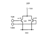
図5のコア回路121Bは、MOSトランジスタQ41,Q42、差動入力端子TCIN,TCINX、およびコア出力端子TCOにより構成されている。 The core circuit 121B shown in FIG. 5 includes MOS transistors Q41 and Q42, differential input terminals TCIN and TCINX, and a core output terminal TCO.
図5のコア回路121Bにおいて、MOSトランジスタQ41のゲートが入力端子TCINに接続され、MOSトランジスタQ42のゲートが入力端子TCINXに接続されている。
MOSトランジスタQ41およびQ42のソースが接地され、ドレイン同士が接続され、ドレイン同士の接続点がコア出力端子TCOに接続され、コア出力端子TCOがインダクタL13の一端に接続されている。
In the core circuit 121B of FIG. 5, the gate of the MOS transistor Q41 is connected to the input terminal TCIN, and the gate of the MOS transistor Q42 is connected to the input terminal TCINX.
The sources of the MOS transistors Q41 and Q42 are grounded, the drains are connected, the connection point between the drains is connected to the core output terminal TCO, and the core output terminal TCO is connected to one end of the inductor L13.
このような構成を有するコア回路121Bにおいて、VCO11による差動発振出力信号が入力されると、これらの入力信号IN,INXの電圧がMOSトランジスタQ41,Q42のしきい値電圧より大きいときに負荷に電流が流れることで半整流を行い、入力信号の周波数に対して2倍の周波数の出力を得る。
In the core circuit 121B having such a configuration, when a differential oscillation output signal from the
図6は、本実施形態に係る2逓倍回路におけるモニタ回路122の第2の構成例を示す回路図である。
FIG. 6 is a circuit diagram showing a second configuration example of the
図6のモニタ回路122Bは、MOSトランジスタQ51,Q52、差動入力端子TCIN,TCINX、およびコア出力端子TCOにより構成されている。
The
図6のモニタ回路122Bにおいて、MOSトランジスタQ51のゲートが入力端子TCINに接続され、MOSトランジスタQ52のゲートが入力端子TCINXに接続されている。
MOSトランジスタQ51およびQ52のソースが接地され、ドレイン同士が接続され、ドレイン同士の接続点がモニタ出力端子TMOに接続され、モニタ出力端子TMOが制御信号生成部123の入力端子に接続されている。
In the
The sources of the MOS transistors Q51 and Q52 are grounded, the drains are connected, the connection point between the drains is connected to the monitor output terminal TMO, and the monitor output terminal TMO is connected to the input terminal of the
このように、モニタ回路122Bは、図5のコア回路121Bと同一の等価回路として構成されており、コア回路121Bと同様の2逓倍動作を行う。
ただし、本実施形態においては、図5および図6に示すように、コア回路121Bを構成する各トランジスタQ41,Q42の素子サイズm=10とすると、モニタ回路122Bを構成する各トランジスタQ51,Q52の素子サイズm=1としている。
これにより、面積や消費電力のオーバーヘッドは小さい。
As described above, the
However, in the present embodiment, as shown in FIGS. 5 and 6, if the element size m of each of the transistors Q41 and Q42 constituting the core circuit 121B is 10, the transistors Q51 and Q52 constituting the
Thereby, the overhead of an area and power consumption is small.
制御信号生成部123は、図2に示すように、基準電流IREFを供給する定電流源1231と、低インピーダンス入力端子がモニタ回路122の出力端子に接続され、高インピーダンス出力端子が定電流源1231に接続されたカンレトミラー回路12321とを有しており、定電流源1231とカンレトミラー回路1232の高インピーダンス出力端子との接続点により制御信号S12を出力する。
As shown in FIG. 2, the
カレントミラー回路1232は、具体的には、図2に示すように、MOSトランジスタQ61,Q62により構成されている。
MOSトランジスタQ61とQ62のソースが電源電位VCCに接続され、モニタ回路12の出力端子TMOにMOSトランジスタQ61のドレイン、並びにMOSトランジスタQ61とQ62のゲートが接続されている。そして、MOSトランジスタQ62のドレインが定電流源1231に接続され、これらの接続点により制御信号S12の出力ノードND13が構成されている。
Specifically, the
The sources of the MOS transistors Q61 and Q62 are connected to the power supply potential VCC, and the drain of the MOS transistor Q61 and the gates of the MOS transistors Q61 and Q62 are connected to the output terminal TMO of the
次に、図2の回路の動作を説明する。 Next, the operation of the circuit of FIG. 2 will be described.
VCO11において、たとえば図示しないPLLのチャージポンプ等から出力される発振制御電圧Vcにより発振周波数が制御され、発振制御電圧Vcで周波数が制御された差動発振出力信号がノードND11,ND12から2逓倍回路12に対して出力される。
In the
VCO11の差動発振出力信号は、2逓倍回路12のコア回路121およびモニタ回路122に並列に入力される。
コア回路121において、VCO11の差動発振出力信号の周波数を2逓倍した信号が生成され、キャパシタC13を介して出力端子TOUTから出力される。
The differential oscillation output signal of the
In the
一方、モニタ回路122においては、コア回路121と同一の回路構成を有していることから、コア回路121の出力信号と等価なレベルの電流信号が生成され、制御信号生成部123に出力される。
制御信号生成部123では、カレントミラー回路1232によってモニタ回路122の出力電流がMOSトランジスタQ62にIDとして取り出され、この電流IDはノードND13に流れる。
そして、モニタ回路122に流れる電流と等価な電流IDと定電流源1231による基準電流IREFとの差分が検出され、ノードND13から検出結果に応じて制御信号S12がVCO11の電流源としてのMOSトランジスタQ13のゲートに出力される。
この場合、モニタ回路122に流れる電流IDが小さければVCO11の出力振幅を大きく(電流源Q13による供給電流を多くする)、モニタ回路122に流れる電流IDが大きければVCO11の出力振幅を小さくする(電流源Q13による供給電流を少なくする)ように制御信号S12が生成される。
このように、VCO11の差動発振出力信号は、その振幅が電流源としてのMOSトランジスタQ13のゲートに印加される2逓倍回路12による制御信号S12で電流量が制御されて調整される。
すなわち、2逓倍回路12の出力レベルが所望の値になるように、VCO11の振幅が制御信号S12で制御される。
これにより、2逓倍回路12の出力レベルは一定となる。
On the other hand, since the
In the
Then, the difference between the current ID equivalent to the current flowing through the
In this case, if the current ID flowing through the
In this way, the differential oscillation output signal of the
That is, the amplitude of the
As a result, the output level of the
また、本実施形態においては、コア回路121A,121Bとモニタ回路122A,122Bの素子サイズの10:1にしていることから、図7に示すように、コア回路121A,121Bとモニタ回路122A,122Bの負荷に流れる電流の比率も10:1となるため、モニタ回路122Aの負荷に流れる電流を測定することで、コア回路121Aの電流を見積もることができる。
In this embodiment, since the element sizes of the
以上説明したように、本実施形態によれば、2逓倍回路12がVCO11の差動発振出力信号の周波数を2逓倍した信号を生成して出力するコア回路121と、VCO11の差動発振出力信号を受けてコア回路121の出力信号と等価なレベルの信号を生成するモニタ回路122と、モニタ回路122の信号出力レベルに基づいて、コア回路121の出力レベルが所望の値となるように制御信号S12を生成してVCO11の電流源としてのMOSトランジスタQ13のゲートに出力する制御信号生成部123と、コア回路121の出力負荷としての集積化されたインダクタL13とを有することから、2逓倍回路12を構成するデバイスの特性が変化したとしても、図8に示すように、従来の逓倍回路に比べて出力レベルを安定に一定レベルに保持することができる。
また、コア回路121A,121Bとモニタ回路122A,122Bの素子サイズの10:1にしていることから、面積や消費電力のオーバーヘッドを小さくすることができる利点がある。
As described above, according to this embodiment, the
Further, since the element sizes of the
図9は、本発明に係る無線通信装置のRFフロントエンド部の一実施形態を示す構成図である。このRFフロントエンド部に、図1〜図8に関連付けて説明した逓倍回路10が局部発振信号を生成する局部発振部に適用されている。
FIG. 9 is a configuration diagram showing an embodiment of the RF front end unit of the wireless communication apparatus according to the present invention. The
この無線通信装置のRFフロントエンド部100は、図9に示すように、アンテナ101、SAWフィルタを含む整合回路102、アンテナスイッチ103、LNA(低雑音増幅器)104、局部発振部105、周波数変換回路としてのミキサ106、SAWフィルタ107、RSSI回路108、ASK変調回路109、およびパワーアンプ(PA)110を有する。
As shown in FIG. 9, an RF front end unit 100 of this wireless communication apparatus includes an
局部発振部105は、VCOを除く位相比較器、分周器、チャージポンプ等を含むPLL部1051、図2に示すVCO11が適用されるVCO1052、同じく図2に示す2逓倍回路12が適用される2逓倍回路1053、VCO1052の出力周波数成分を取り除くためのバンドパスフィルタ(BPF)1054、およびBPF1054の出力を増幅してミキサ106および変調回路109に供給するドライブアンプ1055を有している。
PLL部1051には、たとえば図示しない水晶発振器による周波数16MHz程度の基準信号TCXOが供給され、VCO1052からは周波数が略2.9GHzの差動発振出力信号が出力される。
したがって、2逓倍回路1053から周波数が略5.8MHzの局部発振信号が出力される。
As the
For example, a reference signal TCXO having a frequency of about 16 MHz from a crystal oscillator (not shown) is supplied to the
Therefore, a local oscillation signal having a frequency of about 5.8 MHz is output from the
たとえば、フロントエンド部100においては、たとえば周波数5.9GHz帯の無線信号RFがアンテナ101で受信され、整合回路102、アンテナスイッチ103、さらにLNA104を介してミキサ106に入力される。
そして、ミキサ106において、局部発振部105による局部発振信号とミキシングされ、たとえば40MHzの中間周波が抽出され、SAWフィルタ107、RSSI回路108で所定の処理が施されて、図示しないベースバンド処理部に出力される。
For example, in the front end unit 100, for example, a radio signal RF having a frequency of 5.9 GHz is received by the
Then, in
また、図示しないベースバンド処理部による送信信号TXは、変調回路109において局部発振部105のよる局部発振信号により所定の方式で変調され、パワーアンプ110、アンテナスイッチ103を通して無線により送信される。
A transmission signal TX by a baseband processing unit (not shown) is modulated in a predetermined manner by a local oscillation signal from the
図9の無線通信装置のRFフロントエンド部100においては、上述したように図1〜図8に関連付けて説明した逓倍回路10が局部発振信号を生成する局部発振部105に適用されていることから、レベルが安定した局部発振信号を得ることができる。
その結果、安定したミキシング動作、変調動作を行うこと可能となる。
In the RF front end unit 100 of the wireless communication apparatus of FIG. 9, as described above, the
As a result, stable mixing operation and modulation operation can be performed.
10…逓倍回路、11…VCO、12…2逓倍回路、121…コア回路、122…モニタ回路、123…制御信号生成部、1231…定電流源、1232…カレントミラー回路、100…RFフロントエンド部、101…アンテナ、103…アンテナスイッチ、104…低雑音増幅器(LNA)、105…局部発振部、106…ミキサ、109…変調回路、110…パワーアンプ。
DESCRIPTION OF
Claims (8)
上記信号出力回路による差動発振出力信号の周波数を逓倍した信号を生成して出力するコア回路と、
上記信号出力回路による差動発振出力信号を受けて上記コア回路の出力信号と等価なレベルの信号を生成するモニタ回路と、
上記モニタ回路の信号出力レベルに基づいて、上記コア回路の出力信号のレベルが一定となるように上記制御信号を生成して上記信号出力回路に出力する制御信号生成手段と、を有し、
上記コア回路は、
制御端子並びに入出力用の第1の端子および第2の端子を有する第1から第6のトランジスタと、
第1電源に接続された第1の負荷素子と、
第2電源に接続された第1の電流源と、を含み、
上記第1および第2のトランジスタの第1の端子同士が接続され、その接続点が上記第1の負荷素子に接続され、並びに、第2の端子同士が接続され、その接続点が上記第5のトランジスタの第1の端子に接続され、
上記第3および第4のトランジスタの第1の端子同士が接続され、その接続点が出力負荷に接続され、並びに、第2の端子同士が接続され、その接続点が上記6のトランジスタの第1の端子に接続され、
上記第5および第6のトランジスタの第2の端子同士が接続され、その接続点が上記第1の電流源に接続され、
上記第1、第4および第5のトランジスタの制御端子が上記差動発振出力信号のうちの一方の出力信号の供給ラインに接続され、
上記第2、第3および第6のトランジスタの制御端子が上記差動発振出力信号のうちの他方の出力信号の供給ラインに接続され、
上記モニタ回路は、
制御端子並びに入出力用の第1の端子および第2の端子を有する第7から第12のトランジスタと、
第1電源に接続された第2の負荷素子と、
第2電源に接続された第2の電流源と、を含み、
上記第7および第8のトランジスタの第1の端子同士が接続され、その接続点が上記第2の負荷素子に接続され、並びに、第2の端子同士が接続され、その接続点が上記第11のトランジスタの第1の端子に接続され、
上記第9および第10のトランジスタの第1の端子同士が接続され、その接続点が出力端子に接続され、当該出力端子が上記制御信号生成手段に接続され、並びに、第2の端子同士が接続され、その接続点が上記第12のトランジスタの第1の端子に接続され、
上記第11および第12のトランジスタの第2の端子同士が接続され、その接続点が上記第2の電流源に接続され、
上記第7、第10および第11のトランジスタの制御端子が上記差動発振出力信号のうちの一方の出力信号の供給ラインに接続され、
上記第8、第9および第12のトランジスタの制御端子が上記差動発振出力信号のうちの他方の出力信号の供給ラインに接続され、
上記制御信号生成手段は、
定電流源と、
低インピーダンス入力端子が上記モニタ回路の出力端子に接続され、高インピーダンス出力端子が上記定電流源に接続されたカンレトミラー回路と、を含み、
上記定電流源と上記カンレトミラー回路の高インピーダンス出力端子との接続点により上記制御信号を出力する
逓倍回路。 A multiplication circuit for generating a signal obtained by multiplying the frequency of the differential oscillation output signal by a signal output circuit capable of controlling the amplitude of the differential oscillation output signal according to the control signal,
A core circuit that generates and outputs a signal obtained by multiplying the frequency of the differential oscillation output signal by the signal output circuit;
A monitor circuit that receives a differential oscillation output signal from the signal output circuit and generates a signal having a level equivalent to the output signal of the core circuit;
Control signal generation means for generating the control signal based on the signal output level of the monitor circuit so that the level of the output signal of the core circuit is constant and outputting the control signal to the signal output circuit;
The core circuit is
First to sixth transistors having a control terminal and first and second terminals for input and output;
A first load element connected to a first power source;
A first current source connected to a second power source,
The first terminals of the first and second transistors are connected to each other, the connection point is connected to the first load element, and the second terminals are connected to each other. Connected to the first terminal of the transistor,
The first terminals of the third and fourth transistors are connected to each other, the connection point is connected to the output load, and the second terminals are connected to each other. Connected to the
The second terminals of the fifth and sixth transistors are connected to each other, the connection point is connected to the first current source,
The control terminals of the first, fourth and fifth transistors are connected to a supply line for one of the differential oscillation output signals,
The control terminals of the second, third and sixth transistors are connected to the other output signal supply line of the differential oscillation output signals,
The monitor circuit is
Seventh to twelfth transistors having a control terminal and first and second terminals for input and output;
A second load element connected to the first power source;
A second current source connected to a second power source,
The first terminals of the seventh and eighth transistors are connected to each other, the connection point is connected to the second load element, and the second terminals are connected to each other, and the connection point is the eleventh terminal. Connected to the first terminal of the transistor,
The first terminals of the ninth and tenth transistors are connected to each other, the connection point is connected to the output terminal, the output terminal is connected to the control signal generating means, and the second terminals are connected to each other. The connection point is connected to the first terminal of the twelfth transistor,
The second terminals of the eleventh and twelfth transistors are connected to each other, the connection point is connected to the second current source,
The control terminals of the seventh, tenth and eleventh transistors are connected to one output signal supply line of the differential oscillation output signals,
The control terminals of the eighth, ninth and twelfth transistors are connected to the other output signal supply line of the differential oscillation output signals,
The control signal generating means includes
A constant current source;
A current mirror circuit having a low impedance input terminal connected to the output terminal of the monitor circuit and a high impedance output terminal connected to the constant current source;
A multiplication circuit that outputs the control signal at a connection point between the constant current source and a high impedance output terminal of the current mirror circuit.
請求項1記載の逓倍回路。 2. The multiplier circuit according to claim 1, wherein element sizes of the seventh to twelfth transistors of the monitor circuit are set smaller than element sizes of the first to sixth transistors of the core circuit.
上記電圧制御発振器の差動発振出力信号の周波数を逓倍した信号を生成する逓倍回路と、を有し、
上記逓倍回路は、
上記電圧制御発振器の差動発振出力信号の周波数を逓倍した信号を生成して出力するコア回路と、
上記電圧制御発振器の差動発振出力信号を受けて上記コア回路の出力信号と等価なレベルの信号を生成するモニタ回路と、
上記モニタ回路の信号出力レベルに基づいて、上記コア回路の出力信号のレベルが一定となるように上記制御信号を生成して上記電圧制御発振器に出力する制御信号生成手段と、を含み、
上記コア回路は、
制御端子並びに入出力用の第1の端子および第2の端子を有する第1から第6のトランジスタと、
第1電源に接続された第1の負荷素子と、
第2電源に接続された第1の電流源と、を含み、
上記第1および第2のトランジスタの第1の端子同士が接続され、その接続点が上記第1の負荷素子に接続され、並びに、第2の端子同士が接続され、その接続点が上記第5のトランジスタの第1の端子に接続され、
上記第3および第4のトランジスタの第1の端子同士が接続され、その接続点が出力負荷に接続され、並びに、第2の端子同士が接続され、その接続点が上記6のトランジスタの第1の端子に接続され、
上記第5および第6のトランジスタの第2の端子同士が接続され、その接続点が上記第1の電流源に接続され、
上記第1、第4および第5のトランジスタの制御端子が上記差動発振出力信号のうちの一方の出力信号の供給ラインに接続され、
上記第2、第3および第6のトランジスタの制御端子が上記差動発振出力信号のうちの他方の出力信号の供給ラインに接続され、
上記モニタ回路は、
制御端子並びに入出力用の第1の端子および第2の端子を有する第7から第12のトランジスタと、
第1電源に接続された第2の負荷素子と、
第2電源に接続された第2の電流源と、を含み、
上記第7および第8のトランジスタの第1の端子同士が接続され、その接続点が上記第2の負荷素子に接続され、並びに、第2の端子同士が接続され、その接続点が上記第11のトランジスタの第1の端子に接続され、
上記第9および第10のトランジスタの第1の端子同士が接続され、その接続点が出力端子に接続され、当該出力端子が上記制御信号生成手段に接続され、並びに、第2の端子同士が接続され、その接続点が上記第12のトランジスタの第1の端子に接続され、
上記第11および第12のトランジスタの第2の端子同士が接続され、その接続点が上記第2の電流源に接続され、
上記第7、第10および第11のトランジスタの制御端子が上記差動発振出力信号のうちの一方の出力信号の供給ラインに接続され、
上記第8、第9および第12のトランジスタの制御端子が上記差動発振出力信号のうちの他方の出力信号の供給ラインに接続され、
上記制御信号生成手段は、
定電流源と、
低インピーダンス入力端子が上記モニタ回路の出力端子に接続され、高インピーダンス出力端子が上記定電流源に接続されたカンレトミラー回路と、を含み、
上記定電流源と上記カンレトミラー回路の高インピーダンス出力端子との接続点により形成される出力ノードから上記制御信号を出力し、
上記電圧制御発振器は、
制御端子並びに入出力用の第1の端子および第2の端子を有する第13から第15のトランジスタと、
第1および第2のインダクタと、
第1および第2の可変容量キャパシタと、を含み、
上記第1のインダクタの一端が第1電源に接続され、他端が上記第13のトランジスタの第1の端子に接続され、その接続点に上記第14のトランジスタの制御端子および上記第1の可変容量キャパシタの一端が接続され、
上記第2のインダクタの一端が第1電源に接続され、他端が上記第14のトランジスタの第1の端子に接続され、その接続点に上記第13のトランジスタの制御端子および上記第2の可変容量キャパシタの一端が接続され、
上記第1の可変容量キャパシタの他端と上記第2の可変容量キャパシタの他端に発振制御電圧が供給され、
上記第15のトランジスタの第1の端子が上記第13および第14のトランジスタの第2の端子に接続され、第2の端子が第2電源に接続され、制御端子が上記制御信号生成手段の上記制御信号を出力する上記出力ノードに接続されている
発振回路。 A phase locked loop including a voltage controlled oscillator capable of controlling the amplitude of the differential oscillation output signal in accordance with the control signal;
A multiplication circuit for generating a signal obtained by multiplying the frequency of the differential oscillation output signal of the voltage controlled oscillator,
The multiplier circuit is
A core circuit that generates and outputs a signal obtained by multiplying the frequency of the differential oscillation output signal of the voltage controlled oscillator;
A monitor circuit that receives a differential oscillation output signal of the voltage controlled oscillator and generates a signal having a level equivalent to the output signal of the core circuit;
Control signal generating means for generating the control signal based on the signal output level of the monitor circuit so that the level of the output signal of the core circuit is constant and outputting the control signal to the voltage controlled oscillator,
The core circuit is
First to sixth transistors having a control terminal and first and second terminals for input and output;
A first load element connected to a first power source;
A first current source connected to a second power source,
The first terminals of the first and second transistors are connected to each other, the connection point is connected to the first load element, and the second terminals are connected to each other. Connected to the first terminal of the transistor,
The first terminals of the third and fourth transistors are connected to each other, the connection point is connected to the output load, and the second terminals are connected to each other. Connected to the
The second terminals of the fifth and sixth transistors are connected to each other, the connection point is connected to the first current source,
The control terminals of the first, fourth and fifth transistors are connected to a supply line for one of the differential oscillation output signals,
The control terminals of the second, third and sixth transistors are connected to the other output signal supply line of the differential oscillation output signals,
The monitor circuit is
Seventh to twelfth transistors having a control terminal and first and second terminals for input and output;
A second load element connected to the first power source;
A second current source connected to a second power source,
The first terminals of the seventh and eighth transistors are connected to each other, the connection point is connected to the second load element, and the second terminals are connected to each other, and the connection point is the eleventh terminal. Connected to the first terminal of the transistor,
The first terminals of the ninth and tenth transistors are connected to each other, the connection point is connected to the output terminal, the output terminal is connected to the control signal generating means, and the second terminals are connected to each other. The connection point is connected to the first terminal of the twelfth transistor,
The second terminals of the eleventh and twelfth transistors are connected to each other, the connection point is connected to the second current source,
The control terminals of the seventh, tenth and eleventh transistors are connected to one output signal supply line of the differential oscillation output signals,
The control terminals of the eighth, ninth and twelfth transistors are connected to the other output signal supply line of the differential oscillation output signals,
The control signal generating means includes
A constant current source;
A current mirror circuit having a low impedance input terminal connected to the output terminal of the monitor circuit and a high impedance output terminal connected to the constant current source;
The control signal is output from an output node formed by a connection point between the constant current source and the high impedance output terminal of the current mirror circuit,
The voltage controlled oscillator is
Thirteenth to fifteenth transistors having a control terminal and first and second terminals for input and output;
First and second inductors;
First and second variable capacitors,
One end of the first inductor is connected to the first power supply, the other end is connected to the first terminal of the thirteenth transistor, and the control terminal of the fourteenth transistor and the first variable are connected to the connection point. One end of the capacitor is connected,
One end of the second inductor is connected to the first power supply, the other end is connected to the first terminal of the fourteenth transistor, and the control terminal of the thirteenth transistor and the second variable are connected to the connection point. One end of the capacitor is connected,
An oscillation control voltage is supplied to the other end of the first variable capacitor and the other end of the second variable capacitor,
A first terminal of the fifteenth transistor is connected to a second terminal of the thirteenth and fourteenth transistors, a second terminal is connected to a second power source, and a control terminal is the above-mentioned control signal generating means. An oscillation circuit connected to the output node that outputs a control signal.
請求項3記載の発振回路。 The oscillation circuit according to claim 3, wherein the element sizes of the seventh to twelfth transistors of the monitor circuit are set smaller than the element sizes of the first to sixth transistors of the core circuit.
上記局部発振部は、
制御信号に応じて差動発振出力信号の振幅を制御可能な電圧制御発振器を含む位相同期ループと、
上記電圧制御発振器の差動発振出力信号の周波数を逓倍した信号を生成する逓倍回路と、を有し、
上記逓倍回路は、
上記電圧制御発振器の差動発振出力信号の周波数を逓倍した信号を生成して出力するコア回路と、
上記電圧制御発振器の差動発振出力信号を受けて上記コア回路の出力信号と等価なレベルの信号を生成するモニタ回路と、
上記モニタ回路の信号出力レベルに基づいて、上記コア回路の出力信号のレベルが一定となるように上記制御信号を生成して上記電圧制御発振器に出力する制御信号生成手段と、を含み、
上記コア回路は、
制御端子並びに入出力用の第1の端子および第2の端子を有する第1から第6のトランジスタと、
第1電源に接続された第1の負荷素子と、
第2電源に接続された第1の電流源と、を含み、
上記第1および第2のトランジスタの第1の端子同士が接続され、その接続点が上記第1の負荷素子に接続され、並びに、第2の端子同士が接続され、その接続点が上記第5のトランジスタの第1の端子に接続され、
上記第3および第4のトランジスタの第1の端子同士が接続され、その接続点が出力負荷に接続され、並びに、第2の端子同士が接続され、その接続点が上記第6のトランジスタの第1の端子に接続され、
上記第5および第6のトランジスタの第2の端子同士が接続され、その接続点が上記第1の電流源に接続され、
上記第1、第4および第5のトランジスタの制御端子が上記差動発振出力信号のうちの一方の出力信号の供給ラインに接続され、
上記第2、第3および第6のトランジスタの制御端子が上記差動発振出力信号のうちの他方の出力信号の供給ラインに接続され、
上記モニタ回路は、
制御端子並びに入出力用の第1の端子および第2の端子を有する第7から第12のトランジスタと、
第1電源に接続された第2の負荷素子と、
第2電源に接続された第2の電流源と、を含み、
上記第7および第8のトランジスタの第1の端子同士が接続され、その接続点が上記第2の負荷素子に接続され、並びに、第2の端子同士が接続され、その接続点が上記第11のトランジスタの第1の端子に接続され、
上記第9および第10のトランジスタの第1の端子同士が接続され、その接続点が出力端子に接続され、当該出力端子が上記制御信号生成手段に接続され、並びに、第2の端子同士が接続され、その接続点が上記第12のトランジスタの第1の端子に接続され、
上記第11および第12のトランジスタの第2の端子同士が接続され、その接続点が上記第2の電流源に接続され、
上記第7、第10および第11のトランジスタの制御端子が上記差動発振出力信号のうちの一方の出力信号の供給ラインに接続され、
上記第8、第9および第12のトランジスタの制御端子が上記差動発振出力信号のうちの他方の出力信号の供給ラインに接続され、
上記制御信号生成手段は、
定電流源と、
低インピーダンス入力端子が上記モニタ回路の出力端子に接続され、高インピーダンス出力端子が上記定電流源に接続されたカンレトミラー回路と、を含み、
上記定電流源と上記カンレトミラー回路の高インピーダンス出力端子との接続点により形成される出力ノードから上記制御信号を出力し、
上記電圧制御発振器は、
制御端子並びに入出力用の第1の端子および第2の端子を有する第13から第15のトランジスタと、
第1および第2のインダクタと、
第1および第2の可変容量キャパシタと、を含み、
上記第1のインダクタの一端が第1電源に接続され、他端が上記第13のトランジスタの第1の端子に接続され、その接続点に上記第14のトランジスタの制御端子および上記第1の可変容量キャパシタの一端が接続され、
上記第2のインダクタの一端が第1電源に接続され、他端が上記第14のトランジスタの第1の端子に接続され、その接続点に上記第13のトランジスタの制御端子および上記第2の可変容量キャパシタの一端が接続され、
上記第1の可変容量キャパシタの他端と上記第2の可変容量キャパシタの他端に発振制御電圧が供給され、
上記第15のトランジスタの第1の端子が上記第13および第14のトランジスタの第2の端子に接続され、第2の端子が第2電源に接続され、制御端子が上記制御信号生成手段の上記制御信号を出力する上記出力ノードに接続されている
無線通信装置。 A wireless communication device having a front end unit that performs predetermined processing on at least one of a reception signal and a transmission signal based on a local oscillation signal by a local oscillation unit,
The local oscillator is
A phase locked loop including a voltage controlled oscillator capable of controlling the amplitude of the differential oscillation output signal in accordance with the control signal;
A multiplication circuit for generating a signal obtained by multiplying the frequency of the differential oscillation output signal of the voltage controlled oscillator,
The multiplier circuit is
A core circuit that generates and outputs a signal obtained by multiplying the frequency of the differential oscillation output signal of the voltage controlled oscillator;
A monitor circuit that receives a differential oscillation output signal of the voltage controlled oscillator and generates a signal having a level equivalent to the output signal of the core circuit;
Control signal generating means for generating the control signal based on the signal output level of the monitor circuit so that the level of the output signal of the core circuit is constant and outputting the control signal to the voltage controlled oscillator,
The core circuit is
First to sixth transistors having a control terminal and first and second terminals for input and output;
A first load element connected to a first power source;
A first current source connected to a second power source,
The first terminals of the first and second transistors are connected to each other, the connection point is connected to the first load element, and the second terminals are connected to each other. Connected to the first terminal of the transistor,
The first terminals of the third and fourth transistors are connected to each other, the connection point is connected to the output load, and the second terminals are connected to each other, and the connection point is connected to the first transistor of the sixth transistor. Connected to the terminal 1
The second terminals of the fifth and sixth transistors are connected to each other, the connection point is connected to the first current source,
The control terminals of the first, fourth and fifth transistors are connected to a supply line for one of the differential oscillation output signals,
The control terminals of the second, third and sixth transistors are connected to the other output signal supply line of the differential oscillation output signals,
The monitor circuit is
Seventh to twelfth transistors having a control terminal and first and second terminals for input and output;
A second load element connected to the first power source;
A second current source connected to a second power source,
The first terminals of the seventh and eighth transistors are connected to each other, the connection point is connected to the second load element, and the second terminals are connected to each other, and the connection point is the eleventh terminal. Connected to the first terminal of the transistor,
The first terminals of the ninth and tenth transistors are connected to each other, the connection point is connected to the output terminal, the output terminal is connected to the control signal generating means, and the second terminals are connected to each other. The connection point is connected to the first terminal of the twelfth transistor,
The second terminals of the eleventh and twelfth transistors are connected to each other, the connection point is connected to the second current source,
The control terminals of the seventh, tenth and eleventh transistors are connected to one output signal supply line of the differential oscillation output signals,
The control terminals of the eighth, ninth and twelfth transistors are connected to the other output signal supply line of the differential oscillation output signals,
The control signal generating means includes
A constant current source;
A current mirror circuit having a low impedance input terminal connected to the output terminal of the monitor circuit and a high impedance output terminal connected to the constant current source;
The control signal is output from an output node formed by a connection point between the constant current source and the high impedance output terminal of the current mirror circuit,
The voltage controlled oscillator is
Thirteenth to fifteenth transistors having a control terminal and first and second terminals for input and output;
First and second inductors;
First and second variable capacitors,
One end of the first inductor is connected to the first power supply, the other end is connected to the first terminal of the thirteenth transistor, and the control terminal of the fourteenth transistor and the first variable are connected to the connection point. One end of the capacitor is connected,
One end of the second inductor is connected to the first power supply, the other end is connected to the first terminal of the fourteenth transistor, and the control terminal of the thirteenth transistor and the second variable are connected to the connection point. One end of the capacitor is connected,
An oscillation control voltage is supplied to the other end of the first variable capacitor and the other end of the second variable capacitor,
A first terminal of the fifteenth transistor is connected to a second terminal of the thirteenth and fourteenth transistors, a second terminal is connected to a second power source, and a control terminal is the above-mentioned control signal generating means. A wireless communication apparatus connected to the output node that outputs a control signal.
請求項5記載の無線通信装置。 The wireless communication apparatus according to claim 5, wherein element sizes of the seventh to twelfth transistors of the monitor circuit are set smaller than element sizes of the first to sixth transistors of the core circuit.
所定周波数の受信信号を所定の利得をもって増幅する低雑音増幅器と、
上記低雑音増幅器から出力された所定周波数の受信信号を上記局部発振部による局部発振信号により中間周波数の信号に変換する周波数変換回路と、を有する
請求項5または6記載の無線通信装置。 The front end is
A low noise amplifier for amplifying a received signal of a predetermined frequency with a predetermined gain;
The radio communication apparatus according to claim 5, further comprising: a frequency conversion circuit configured to convert a reception signal having a predetermined frequency output from the low noise amplifier into a signal having an intermediate frequency by a local oscillation signal generated by the local oscillation unit.
送信信号を上記局部発振部による局部発振信号により所定の方式で変調する変調回路と、
変調回路により変調された送信信号を無線により送信させるパワー増幅器と、を有する
請求項5から7のいずれか一に記載の無線通信装置。 The front end is
A modulation circuit that modulates a transmission signal in a predetermined manner by a local oscillation signal from the local oscillation unit;
A wireless communication device according to any one of claims 5 to 7, further comprising: a power amplifier that wirelessly transmits a transmission signal modulated by the modulation circuit.
Priority Applications (1)
| Application Number | Priority Date | Filing Date | Title |
|---|---|---|---|
| JP2004134279A JP4779305B2 (en) | 2004-04-28 | 2004-04-28 | Multiplier circuit, oscillation circuit, and wireless communication device |
Applications Claiming Priority (1)
| Application Number | Priority Date | Filing Date | Title |
|---|---|---|---|
| JP2004134279A JP4779305B2 (en) | 2004-04-28 | 2004-04-28 | Multiplier circuit, oscillation circuit, and wireless communication device |
Publications (3)
| Publication Number | Publication Date |
|---|---|
| JP2005318300A JP2005318300A (en) | 2005-11-10 |
| JP2005318300A5 JP2005318300A5 (en) | 2007-06-07 |
| JP4779305B2 true JP4779305B2 (en) | 2011-09-28 |
Family
ID=35445268
Family Applications (1)
| Application Number | Title | Priority Date | Filing Date |
|---|---|---|---|
| JP2004134279A Expired - Fee Related JP4779305B2 (en) | 2004-04-28 | 2004-04-28 | Multiplier circuit, oscillation circuit, and wireless communication device |
Country Status (1)
| Country | Link |
|---|---|
| JP (1) | JP4779305B2 (en) |
Families Citing this family (5)
| Publication number | Priority date | Publication date | Assignee | Title |
|---|---|---|---|---|
| JP5117426B2 (en) * | 2009-02-25 | 2013-01-16 | ルネサスエレクトロニクス株式会社 | Oscillator circuit |
| US10547274B2 (en) | 2015-10-26 | 2020-01-28 | Seiko Epson Corporation | Oscillation module, electronic device, and moving object |
| JP6798778B2 (en) * | 2015-10-26 | 2020-12-09 | セイコーエプソン株式会社 | Oscillator modules, electronic devices and mobiles |
| JP6672698B2 (en) * | 2015-10-26 | 2020-03-25 | セイコーエプソン株式会社 | Oscillation module, electronic equipment and moving object |
| JP7064524B2 (en) * | 2020-03-19 | 2022-05-10 | セイコーエプソン株式会社 | Oscillator modules, electronic devices and mobiles |
Family Cites Families (6)
| Publication number | Priority date | Publication date | Assignee | Title |
|---|---|---|---|---|
| JPS6352502A (en) * | 1986-08-22 | 1988-03-05 | Matsushita Electric Ind Co Ltd | Multiplier |
| JPS63146603A (en) * | 1986-12-10 | 1988-06-18 | Matsushita Electric Ind Co Ltd | Multiplier |
| JPH11308103A (en) * | 1998-04-17 | 1999-11-05 | Nec Corp | Method and circuit for reducing noise of pll oscillation circuit |
| JP2001285118A (en) * | 2000-03-29 | 2001-10-12 | Matsushita Electric Ind Co Ltd | Radio communication equipment |
| JP2002009553A (en) * | 2000-06-19 | 2002-01-11 | Matsushita Electric Ind Co Ltd | Detection circuit |
| JP2003046339A (en) * | 2001-07-30 | 2003-02-14 | Niigata Seimitsu Kk | Am detection circuit |
-
2004
- 2004-04-28 JP JP2004134279A patent/JP4779305B2/en not_active Expired - Fee Related
Also Published As
| Publication number | Publication date |
|---|---|
| JP2005318300A (en) | 2005-11-10 |
Similar Documents
| Publication | Publication Date | Title |
|---|---|---|
| JP4713939B2 (en) | Voltage controlled oscillator and wireless communication device using the same | |
| US7239209B2 (en) | Serially RC coupled quadrature oscillator | |
| JP5027472B2 (en) | Oscillator and information device using the same | |
| US7839229B2 (en) | Voltage-controlled oscillator and communication device using the same | |
| US8502614B2 (en) | Variable inductor, and oscillator and communication system using the same | |
| US7375596B2 (en) | Quadrature voltage controlled oscillator | |
| US6606489B2 (en) | Differential to single-ended converter with large output swing | |
| CN104160627B (en) | Voltage controlled oscillator, signal generating apparatus, and electronic apparatus | |
| US20090128240A1 (en) | Oscillator, pll circuit, receiver and transmitter | |
| WO2012166502A1 (en) | Method and apparatus for local oscillation distribution | |
| JP5487073B2 (en) | High frequency signal processor | |
| US7911281B2 (en) | PLL circuit and radio communication apparatus | |
| JP2007282244A (en) | Four-phase voltage controlled oscillator comprising coupling capacitor | |
| US8792845B2 (en) | Oscillator | |
| CN105281669B (en) | System and method for voltage controlled oscillator | |
| JP4779305B2 (en) | Multiplier circuit, oscillation circuit, and wireless communication device | |
| US20040032303A1 (en) | Oscillator transmission circuit and radio apparatus | |
| CN100533982C (en) | Oscillator circuit | |
| US6987423B2 (en) | Two port voltage controlled oscillator for use in wireless personal area network synthesizers | |
| JP2009278616A (en) | Voltage controlled oscillator, and pll circuit, and radio communication device each including the same | |
| US8219054B2 (en) | Oscillating circuit and radio communication apparatus | |
| US7109798B2 (en) | Method and system for common mode feedback circuitry for RF buffers | |
| JP2007104355A (en) | Mixer/oscillator apparatus for tuner | |
| JP5553855B2 (en) | Voltage controlled oscillator and information device using the same | |
| US7057466B2 (en) | Varactor-based ring oscillator |
Legal Events
| Date | Code | Title | Description |
|---|---|---|---|
| A521 | Written amendment |
Free format text: JAPANESE INTERMEDIATE CODE: A523 Effective date: 20070417 |
|
| A621 | Written request for application examination |
Free format text: JAPANESE INTERMEDIATE CODE: A621 Effective date: 20070417 |
|
| A131 | Notification of reasons for refusal |
Free format text: JAPANESE INTERMEDIATE CODE: A131 Effective date: 20100413 |
|
| A521 | Written amendment |
Free format text: JAPANESE INTERMEDIATE CODE: A523 Effective date: 20100607 |
|
| A131 | Notification of reasons for refusal |
Free format text: JAPANESE INTERMEDIATE CODE: A131 Effective date: 20110315 |
|
| A521 | Written amendment |
Free format text: JAPANESE INTERMEDIATE CODE: A523 Effective date: 20110506 |
|
| TRDD | Decision of grant or rejection written | ||
| A01 | Written decision to grant a patent or to grant a registration (utility model) |
Free format text: JAPANESE INTERMEDIATE CODE: A01 Effective date: 20110607 |
|
| A01 | Written decision to grant a patent or to grant a registration (utility model) |
Free format text: JAPANESE INTERMEDIATE CODE: A01 |
|
| A61 | First payment of annual fees (during grant procedure) |
Free format text: JAPANESE INTERMEDIATE CODE: A61 Effective date: 20110620 |
|
| FPAY | Renewal fee payment (event date is renewal date of database) |
Free format text: PAYMENT UNTIL: 20140715 Year of fee payment: 3 |
|
| FPAY | Renewal fee payment (event date is renewal date of database) |
Free format text: PAYMENT UNTIL: 20140715 Year of fee payment: 3 |
|
| LAPS | Cancellation because of no payment of annual fees |