JP4775813B2 - Receiver IC - Google Patents
Receiver IC Download PDFInfo
- Publication number
- JP4775813B2 JP4775813B2 JP2006090079A JP2006090079A JP4775813B2 JP 4775813 B2 JP4775813 B2 JP 4775813B2 JP 2006090079 A JP2006090079 A JP 2006090079A JP 2006090079 A JP2006090079 A JP 2006090079A JP 4775813 B2 JP4775813 B2 JP 4775813B2
- Authority
- JP
- Japan
- Prior art keywords
- amplifier
- crystal filter
- capacitor
- received signal
- parallel
- Prior art date
- Legal status (The legal status is an assumption and is not a legal conclusion. Google has not performed a legal analysis and makes no representation as to the accuracy of the status listed.)
- Expired - Fee Related
Links
- 239000013078 crystal Substances 0.000 claims description 62
- 239000003990 capacitor Substances 0.000 claims description 55
- 238000010586 diagram Methods 0.000 description 9
- 230000000694 effects Effects 0.000 description 4
- 230000035945 sensitivity Effects 0.000 description 4
- 238000001514 detection method Methods 0.000 description 3
- 238000001914 filtration Methods 0.000 description 3
- 239000010453 quartz Substances 0.000 description 2
- VYPSYNLAJGMNEJ-UHFFFAOYSA-N silicon dioxide Inorganic materials O=[Si]=O VYPSYNLAJGMNEJ-UHFFFAOYSA-N 0.000 description 2
- 101100191136 Arabidopsis thaliana PCMP-A2 gene Proteins 0.000 description 1
- 101100048260 Saccharomyces cerevisiae (strain ATCC 204508 / S288c) UBX2 gene Proteins 0.000 description 1
- 230000003321 amplification Effects 0.000 description 1
- 230000002708 enhancing effect Effects 0.000 description 1
- 238000003199 nucleic acid amplification method Methods 0.000 description 1
Images

Landscapes
- Electric Clocks (AREA)
- Electromechanical Clocks (AREA)
- Noise Elimination (AREA)
Description
本発明は、受信した信号を増幅し、検波し、二値化した信号を出力する電波時計などに用いる受信ICに関するものである。 The present invention relates to a receiving IC used in a radio timepiece or the like that amplifies a received signal, detects it, and outputs a binarized signal.
従来、電波時計などに用いる時刻信号は、アンテナで受信した標準電波信号を増幅し、検波し、二値化して形成される。このため、電波時計用受信ICにおいては、検波回路の前に、増幅回路から構成されるAGC(Auto Gain Control) アンプ(AMP)などのアンプと、増幅回路から構成される固定ゲインアンプ(PostAMP)とを配置する。さらに、電波時計用の信号の搬送波は精度の高い単一周波数(例えば、日本においては、独立行政法人通信総合研究所によって提供される電波時計受信電波では40kHz又は60kHz)であるために、ノイズ除去の目的でAGCアンプと固定ゲインアンプとの間に水晶フィルタを挿入するのが一般的である。 Conventionally, a time signal used in a radio timepiece or the like is formed by amplifying, detecting, and binarizing a standard radio signal received by an antenna. For this reason, in the radio wave clock receiver IC, before the detection circuit, an amplifier such as an AGC (Auto Gain Control) amplifier (AMP) composed of an amplifier circuit and a fixed gain amplifier (PostAMP) composed of the amplifier circuit. And place. Further, since the carrier wave of the signal for the radio clock is a single frequency with high accuracy (for example, 40 kHz or 60 kHz for the radio clock received radio wave provided by the Communications Research Laboratory in Japan) For this purpose, a crystal filter is generally inserted between the AGC amplifier and the fixed gain amplifier.
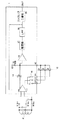
図7に、従来の電波時計などに用いられる受信回路が形成された受信ICの構成を示す。受信アンテナから受信した周波数が40kHzもしくは60kHzの電波はアンテナ端にて電圧信号に変換され、AGCアンプ101により増幅される。増幅された信号は、ノイズを除去するためにフィルタによってろ波される。フィルタとしては外付けの水晶フィルタ102が用いられる。フィルタによりろ波された信号は、Postアンプ104により更に増幅される。増幅された信号は、整流器により整流され、ローパスフィルタ(LPF)によりろ波され、その後コンパレータにより二値化されて受信ICから出力される。二値化された信号から時刻信号が形成される。図7においては水晶フィルタ102は、コイルL、容量C1及び抵抗Rが接続された直列回路及び等価並列容量C0 から構成された等価回路で表示されている。等価並列容量C0 は、水晶フィルタ固有のものであり、AGCアンプを通過してくる高周波成分のノイズを透過させる原因となっている。この高周波成分ノイズを除去するためにAGCアンプ101の逆相出力端子とPostアンプ104の入力端子との間に高周波成分ノイズをキャンセルする容量(Cc )103が挿入されている。Postアンプ104には電源105に付加された入力抵抗(Rin)106が接続されている。
FIG. 7 shows a configuration of a receiving IC in which a receiving circuit used in a conventional radio timepiece or the like is formed. A radio wave having a frequency of 40 kHz or 60 kHz received from the receiving antenna is converted into a voltage signal at the antenna end and amplified by the
引用文献1には、低電流、低占有面積で所望の周波数での差動増幅回路のゲインを大きくすることができ、電波時計のような単一搬送周波数の電波の受信の増幅等に非常に有用な増幅回路が開示されている(引用文献1の図1参照)。ここで開示された差動増幅回路は、一対のトランジスタ及びこの一対のトランジスタの出力端側に設けられた一対の負荷を有する差動増幅回路において、この差動増幅回路の負荷として所望の周波数において利得を決定するインピーダンスとしての一対の容量と、差動増幅回路のバイアス電流を相殺する一対の電流源と、出力バイアス電圧を決定するための一対の高抵抗とを並列に付加した構成を有している。
従来、前述した水晶フィルタの等価並列容量(C0 )による高周波成分ノイズをキャンセルするキャンセル容量(Cc )は、受信IC内に設けられている。しかしながら、水晶フィルタの等価並列容量は、水晶の形状やサイズ等により異なることが多い。そのため受信ICに水晶フィルタを取付けた場合、受信ICのあるものは内蔵したキャンセル容量と一致しない水晶フィルタを使用することがある。そのような場合、高周波雑音のキャンセル効果が良くなく、Postアンプ104で高周波雑音を増幅してしまうために受信信号と雑音の比が悪くなり、電波時計としての受信感度の向上の妨げになることが多い。
本発明は、このような事情によりなされたものであり、内蔵したキャンセル容量を水晶フィルタの等価並列容量に適合するように構成することにより高周波雑音のキャンセル効果を高くする受信ICを提供する。
Conventionally, a cancel capacitor (Cc) for canceling high-frequency component noise due to the above-described equivalent parallel capacitor (C0) of the crystal filter is provided in the receiving IC. However, the equivalent parallel capacitance of the crystal filter often varies depending on the shape and size of the crystal. For this reason, when a crystal filter is attached to the receiving IC, some of the receiving ICs may use a crystal filter that does not match the built-in canceling capacity. In such a case, the high frequency noise canceling effect is not good, and the
The present invention has been made under such circumstances, and provides a receiver IC that enhances the cancellation effect of high-frequency noise by configuring the built-in cancellation capacitor so as to match the equivalent parallel capacitance of the crystal filter.
本発明の受信ICの一態様は、受信信号を増幅する第1の増幅器と、前記第1の増幅器により増幅された前記受信信号のノイズを前記第1の増幅器の正相出力端子に接続された水晶フィルタによって除去した後にノイズが除去された前記受信信号を増幅する第2の増幅器と前記第1の増幅器の逆相出力端子と前記第2の増幅器の入力端子間に設けられ、前記水晶フィルタの等価並列容量を透過するノイズをキャンセルするキャンセル容量とを備え、前記キャンセル容量は、前記第1の増幅器の逆相出力端子に接続され、バッファと容量とが直列に接続された直列回路が複数並列に接続され、これら容量が互いに異なる容量値を有する第1の並列回路と、前記容量を選択する第1のデコーダとを有し、前記水晶フィルタは、前記第1の増幅器の前記正相出力端子に接続され、バッファと水晶フィルタ素子とが直列に接続された直列回路が、複数並列に接続され、当該水晶フィルタ素子が互いに異なる等価並列容量を有する第2の並列回路と、前記水晶フィルタ素子を選択する第2のデコーダとを有し、前記第2のデコーダによって、前記バッファと前記水晶フィルタ素子との1つの組合せが選択され、前記第1のデコーダによって、前記選択された水晶フィルタ素子に対応した前記バッファと前記容量との組合せが選択されることによってキャンセル容量値が切り替えられることを特徴としている。前記第2の増幅器により増幅された前記受信信号を整流する整流器、前記整流器により整流された前記受信信号をろ波するローパスフィルタ及び前記ローパスフィルタによりろ波された前記受信信号を二値化するコンパレータを更に備えているようにしても良い。前記第2の増幅器に印加されるバイアス電源に挿入される入力抵抗は、抵抗値の制御が可能な可変抵抗であるようにしても良い。
According to one aspect of the receiving IC of the present invention, a first amplifier for amplifying a received signal, and noise of the received signal amplified by the first amplifier are connected to a positive phase output terminal of the first amplifier. A second amplifier that amplifies the received signal from which noise has been removed after being removed by the crystal filter, a negative phase output terminal of the first amplifier, and an input terminal of the second amplifier; A cancel capacitor for canceling noise passing through the equivalent parallel capacitor, wherein the cancel capacitor is connected to a reverse phase output terminal of the first amplifier, and a plurality of series circuits in which a buffer and a capacitor are connected in series are connected in parallel. A first parallel circuit having a capacitance value different from each other, and a first decoder for selecting the capacitance, wherein the crystal filter includes the first amplifier of the first amplifier. A series circuit in which a buffer and a crystal filter element are connected in series, connected to the positive phase output terminal, and a plurality of parallel circuits connected in parallel, and the crystal filter elements have different equivalent parallel capacitances; A second decoder for selecting the crystal filter element, the second decoder selects one combination of the buffer and the crystal filter element, and the first decoder selects the selected The cancel capacitance value is switched by selecting a combination of the buffer and the capacitor corresponding to the crystal filter element. A rectifier that rectifies the received signal amplified by the second amplifier, a low-pass filter that filters the received signal rectified by the rectifier, and a comparator that binarizes the received signal filtered by the low-pass filter May be further provided. The input resistor inserted into the bias power source applied to the second amplifier may be a variable resistor whose resistance value can be controlled.
本発明は、キャンセル容量の容量値を制御することによって、水晶フィルタでろ波できず通過する高周波雑音のキャンセル効果を高くして受信感度を向上させる。 The present invention improves the reception sensitivity by controlling the capacitance value of the cancellation capacitor, thereby enhancing the cancellation effect of high-frequency noise that cannot pass through the crystal filter and passes therethrough.
以下、実施例を参照して発明の実施の形態を説明する。 Hereinafter, embodiments of the invention will be described with reference to examples.
まず、図1乃至図4を参照して実施例1を説明する。
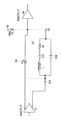
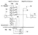
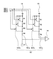
図1は、アンテナ及び水晶フィルタを外付けし、受信した信号を増幅し、検波し、二値化した信号を出力する電波時計等に用いる受信ICの概略ブロック図、図2は、図1の増幅器及び水晶フィルタの部分の構成を示す回路図、図3は、図2に示されるキャンセル容量の詳細な構造を示す部分回路図、図4は、水晶フィルタのろ波特性を説明する周波数特性図である。
First,
FIG. 1 is a schematic block diagram of a receiving IC used in a radio clock or the like that externally attaches an antenna and a crystal filter, amplifies a received signal, detects it, and outputs a binarized signal. FIG. FIG. 3 is a partial circuit diagram showing a detailed structure of the canceling capacitor shown in FIG. 2, and FIG. 4 is a frequency characteristic for explaining the filtering characteristics of the crystal filter. FIG.
図1に示すように、電波時計などに用いる時刻信号は、アンテナ2で受信した信号を増幅し、検波し、二値化して形成される。このため、電波時計用受信IC1には、検波回路の前に、増幅回路から構成されるAGCアンプなどのアンプ11と、増幅回路から構成される固定ゲインアンプ(Postアンプ)14とが配置されている。この受信IC1において、アンテナ2から受信した周波数が40kHzもしくは60kHzの電波はアンテナ端にて電圧信号に変換され、AGCアンプ11により増幅される。増幅された信号は、ノイズを除去するためにろ波される。ろ波フィルタとしては外付けの水晶フィルタ12が用いられる。
As shown in FIG. 1, a time signal used for a radio timepiece or the like is formed by amplifying a signal received by an
この実施例で用いられる水晶フィルタ12は、並列接続された3個の水晶フィルタ12a、12b、12cから構成され、それぞれ40kHz、60kHz、77.5kHzの周波数の信号をろ波する。各水晶フィルタにはスイッチ18が設けられており、スイッチ18の断続によって所望の信号の周波数を選択するように構成されている。水晶フィルタ12は、AGCアンプ11の正相出力端子に接続され、Postアンプ14の入力端子に接続されている。水晶フィルタ12によりろ波された信号は、Postアンプ14により増幅される。増幅された信号は、整流器17により整流され、その後、ローパスフィルタ(LPF)19によりろ波される。その後、ろ波された信号は、コンパレータ20により二値化されて出力される。二値化された信号から時刻信号が形成される。
The
図2においては、水晶フィルタ12はコイルL、容量C1及び抵抗Rが接続された直列回路及び等価並列容量C0 から構成された等価回路で表示されている。等価並列容量C0 は、水晶フィルタ固有のものであり、AGCアンプを通過してくる高周波成分のノイズを透過させる原因になっている(図4参照)。この高周波成分のノイズは、1MHz程度以上の高周波領域で生じるが、この高周波成分ノイズを除去するためにAGCアンプ11の逆相出力端子とPostアンプ14の入力端子との間に高周波成分ノイズをキャンセルする可変のキャンセル容量(Cc )13が挿入されている。また、Postアンプ14にはPostアンプ14にバイアス電圧を印加する電源15が接続され、電源15には入力抵抗(RIN)16が接続されている。
In FIG. 2, the
この実施例の特徴は、キャンセル容量(Cc )13の容量値を可変にしたことにある。即ち、この実施例では、受信IC1に設けられたキャンセル容量は、互いに異なる容量値を有する複数の容量とこれら容量のそれぞれに設けられたスイッチ回路とから構成され、スイッチ回路は外部から制御できるように構成されている。
The feature of this embodiment is that the capacitance value of the cancel capacitor (Cc) 13 is made variable. That is, in this embodiment, the canceling capacitor provided in the
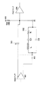
図3は、このキャンセル容量の構成を詳細に説明している。
図3において、キャンセル容量(Cc )13は、容量13a(Cc01 、Cc02 、Cc03 、Cc04 )、バッファ13b及びデコーダ13cから構成されている。容量13aは、例えば、0.7pF(Cc01 )、0.9pF(Cc02 )、1.1pF(Cc03 )、1.3pF(Cc04 )の4種類が受信ICに内蔵されている。各容量は、バッファ13bを介して、デコーダ13cに接続される。そして、デコーダ13cの入力信号cc1、cc2によって4種類の容量値からいずれかの容量が選択される。
また、水晶フィルタ12も同じようにスイッチ18によってその周波数が選択される。スイッチ18は、バッファ18a及びデコーダ18bから構成され、デコーダ18bの入力信号XOA 、XOB によって3種類の周波数値からいずれかの周波数が選択される。
FIG. 3 illustrates the configuration of the cancel capacity in detail.
In FIG. 3, the cancel capacitor (Cc) 13 includes a
Similarly, the frequency of the
以上のように、受信ICに組み込まれ、水晶フィルタの等価並列容量(C0 )を通過する高周波成分ノイズをキャンセルするキャンセル容量(Cc )は、容量値を制御できる可変構造に構成されているので、用意した水晶フィルタが多少期待した値から離れた値を有する等価並列容量(C0 )を持っていても最適な容量に制御することができる。その結果、高周波雑音のキャンセル効果が良くなり、電波時計としての受信感度の向上につながるものである。 As described above, the cancel capacitor (Cc) that is incorporated in the receiver IC and cancels the high-frequency component noise that passes through the equivalent parallel capacitor (C0) of the crystal filter has a variable structure that can control the capacitance value. Even if the prepared crystal filter has an equivalent parallel capacitance (C0) having a value slightly different from the expected value, it can be controlled to the optimum capacitance. As a result, the effect of canceling high-frequency noise is improved, leading to an improvement in reception sensitivity as a radio timepiece.
次に、図5を参照して実施例2を説明する。
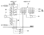
図5は、受信した信号を増幅し、検波し、二値化した信号を出力する電波時計等に用いる受信ICに外付けされた水晶フィルタの等価並列容量を透過する高周波成分ノイズをキャンセルするキャンセル容量及び水晶フィルタの詳細な構造を示す部分回路図である。この実施例の受信ICは、Postアンプに接続された入力抵抗が可変であることに特徴がある。
Next, Example 2 will be described with reference to FIG.
FIG. 5 shows a cancellation for canceling high-frequency component noise transmitted through an equivalent parallel capacitance of a crystal filter externally attached to a receiving IC used for a radio wave clock or the like that amplifies and detects a received signal and outputs a binarized signal. It is a partial circuit diagram which shows the detailed structure of a capacity | capacitance and a crystal filter. The receiving IC of this embodiment is characterized in that the input resistance connected to the Post amplifier is variable.
電波時計などに用いる時刻信号は、アンテナで受信した信号を増幅し、検波し、二値化して形成される。このため、電波時計用受信ICにおいては、検波回路の前に、増幅回路から構成されるAGCアンプなどのアンプ21と、増幅回路から構成される固定ゲインアンプ(Postアンプ)24とが配置されている。この受信ICにおいて、アンテナから受信した周波数が40kHzもしくは60kHzの電波はアンテナ端にて電圧信号に変換され、AGCアンプ21により増幅される。増幅された信号はノイズを除去するためにろ波フィルタによってろ波される。ろ波フィルタとしては外付けの水晶フィルタ22が用いられる。
A time signal used for a radio timepiece or the like is formed by amplifying, detecting, and binarizing a signal received by an antenna. For this reason, in the radio wave clock receiver IC, an
この実施例で用いられる水晶フィルタ22は、並列接続された3個の水晶フィルタから構成され、それぞれ40kHz、60kHz、77.5kHzの周波数の信号をろ波する。各水晶フィルタにはスイッチ28が設けられており、スイッチ28の断続によって所望の信号の周波数を選択するように構成されている。水晶フィルタ22は、AGCアンプ21の正相出力端子に接続され、Postアンプ24の入力端子に接続されている。
水晶フィルタ22によりろ波された信号は、Postアンプ24により増幅される。増幅された信号は、整流器により整流され、その後、ローパスフィルタ(LPF)によりろ波される。その後、ろ波された信号は、コンパレータにより二値化されて出力される。二値化された信号から時刻信号が形成される。
The
The signal filtered by the
水晶フィルタ22の等価並列容量C0 は、水晶フィルタ固有のものであり、AGCアンプを通過してくる高周波成分のノイズを透過させる原因になっている。この高周波成分ノイズを除去するためにAGCアンプ21の逆相出力端子とPostアンプ24の入力端子との間に高周波成分ノイズをキャンセルするキャンセル容量(Cc )23を挿入する。また、Postアンプ24にはこのPostアンプ24にバイアス電圧を印加する電源25が接続され、電源25には入力抵抗(RIN)26が接続されている。
この実施例の特徴は、キャンセル容量(Cc )23の容量値を可変にし、さらに入力抵抗26の抵抗値を可変にすることを特徴としている。即ち、この実施例では、受信ICに設けられたキャンセル容量は、互いに異なる容量値を有する複数の容量とこれら容量のそれぞれに設けられたスイッチ回路とから構成され、スイッチ回路は外部から制御できるように構成されている。また、受信ICに設けられた入力抵抗は、互いに異なる抵抗値を有する複数の抵抗とこれら抵抗のそれぞれに設けられたスイッチとから構成され、スイッチは外部から制御できるように構成されている。
The equivalent parallel capacitance C0 of the
The feature of this embodiment is that the capacitance value of the cancel capacitor (Cc) 23 is made variable and the resistance value of the
図5は、入力抵抗及びキャンセル容量の構成を詳細に説明している。図において、入力抵抗(RIN)26は、抵抗26a(R1 、R2 、R3 、R4 )、スイッチ26b及びデコーダ26cから構成されている。入力抵抗26は、例えば、25kΩ(R1 )、50kΩ(R2 )、100kΩ(R3 )、200kΩ(R4 )の4種類が受信ICに内蔵されている。入力抵抗26の各抵抗は、スイッチ26bを介して、デコーダ26cに接続される。そして、デコーダ26cの入力信号RI1 、RI2 によって4種類の抵抗値からいずれかの抵抗が選択される。
FIG. 5 illustrates in detail the configuration of the input resistor and the cancel capacitor. In the figure, an input resistor (RIN) 26 comprises a
水晶フィルタのQ値(f0 /fB )は、Postアンプ24に接続される入力抵抗(RIN)26の抵抗値に依存する。水晶フィルタのQ値は、水晶フィルタの共振周波数(f0 )(例えば、40kHz)と周波数通過帯域(fB )(例えば、3〜5Hz程度)との比で表わされ、周波数特性の共振周波数の鋭さを表している。周波数通過帯域が大きいとQ値は小さくなり、Q値が小さいとAGCアンプからのノイズを多く通過させてしまう。したがって、Q値はできるだけ大きい方が良く、そのためには入力抵抗26(RIN)を小さくする必要がある。また、水晶フィルタを通過し、Postアンプに入力される信号の利得(G(XI))は、RIN/(CI+RIN)で表される。CIは、水晶の固有のインピーダンスである。G(XI )が大きいとPostアンプに入力される信号が大きくなる。したがって、入力抵抗26(RIN)を大きくするほど信号を多く通すことが可能になる。
The Q value (f0 / fB) of the crystal filter depends on the resistance value of the input resistor (RIN) 26 connected to the
以上の通りであるから可変構造の入力抵抗(RIN)を適宜調整して周波数通過帯域(fB )及びPostアンプに入力される信号の利得(G(XI))の最適値を選択することにより、所定の受信ICに水晶フィルタを外付けした時に、その外付け水晶フィルタの特性に関わらず電波信号の損失を防いで受信感度の更なる向上を期待することができる。 As described above, by appropriately adjusting the variable structure input resistance (RIN) and selecting the optimum value of the frequency passband (fB) and the gain (G (XI)) of the signal input to the Post amplifier, When a crystal filter is externally attached to a predetermined receiving IC, it is possible to expect a further improvement in reception sensitivity by preventing loss of radio signal regardless of the characteristics of the external crystal filter.
なお、本発明は上記実施の形態に限られるものではない。上記実施の形態では受信IC1に設けられたキャンセル容量は、互いに異なる容量値を有する容量を並列接続したが(図3参照)、互いに同じ容量値を有する容量を並列接続し、スイッチ回路の断続によってキャンセル容量の容量値を制御しても良い。
The present invention is not limited to the above embodiment. In the above embodiment, the cancel capacitors provided in the receiving
また、上記実施の形態では受信IC1に設けられたキャンセル容量は、複数の容量を並列接続したが(図3参照)、これを直列接続とし、直列接続された各々の容量の両端子間に各々の容量に対して並列にスイッチ回路を接続し、スイッチ回路の断続によってキャンセル容量の容量値を制御することができる。
図6は、この直列接続されたキャンセル容量の構成を詳細に説明している。
キャンセル容量(Cc )13′は、容量13′a(Cc01 、Cc02 、 Cc03 、Cc04 )、バッファ(BUF)13´b及びスイッチ13c(SEL1〜SEL4)から構成されている。4つの容量13′aは、AGCアンプ11の逆相出力端子とPostアンプ14の入力端子間に直列接続され、直列接続された各々のキャンセル容量13′の両端子間に各々の容量に対して並列にスイッチ13′cを接続し、スイッチ回路の断続によってキャンセル容量の容量値を制御する。
In the above embodiment, the canceling capacitor provided in the receiving
FIG. 6 explains the configuration of the cancel capacitors connected in series in detail.
The cancel capacitor (Cc) 13 'includes a capacitor 13'a (Cc01, Cc02, Cc03, Cc04), a buffer (BUF) 13'b, and a
1・・・受信IC 2・・・アンテナ
11、21・・・AGCアンプ(第1の増幅器)
12、12a、12b、12c、22・・・水晶フィルタ
13、13′、23・・・キャンセル容量(Cc )
13a、13′a・・・容量(Cc01 、Cc02 、Cc03 、Cc04 )
13b、13′b・・・バッファ 13c・・・デコーダ
13′c・・・スイッチ
14、24・・・Postアンプ(第2の増幅器)
15、25・・・電源 16、26・・・入力抵抗(RIN)
17・・・整流器 18・・・水晶フィルタのスイッチ
18a・・・バッファ 18b・・・デコーダ
19・・・ローパスフィルタ(LPF) 20・・・コンパレータ
26a・・・抵抗(R1 、R2 、R3 、R4 )
26b・・・入力抵抗のスイッチ 26c・・・デコーダ
DESCRIPTION OF
12, 12a, 12b, 12c, 22 ...
13a, 13'a ... Capacity (Cc01, Cc02, Cc03, Cc04)
13b, 13'b ... buffer 13c ... decoder 13'c ... switch 14, 24 ... Post amplifier (second amplifier)
15, 25 ...
DESCRIPTION OF
26b: Input resistance switch 26c: Decoder
Claims (3)
Priority Applications (1)
| Application Number | Priority Date | Filing Date | Title |
|---|---|---|---|
| JP2006090079A JP4775813B2 (en) | 2006-03-29 | 2006-03-29 | Receiver IC |
Applications Claiming Priority (1)
| Application Number | Priority Date | Filing Date | Title |
|---|---|---|---|
| JP2006090079A JP4775813B2 (en) | 2006-03-29 | 2006-03-29 | Receiver IC |
Publications (2)
| Publication Number | Publication Date |
|---|---|
| JP2007267094A JP2007267094A (en) | 2007-10-11 |
| JP4775813B2 true JP4775813B2 (en) | 2011-09-21 |
Family
ID=38639630
Family Applications (1)
| Application Number | Title | Priority Date | Filing Date |
|---|---|---|---|
| JP2006090079A Expired - Fee Related JP4775813B2 (en) | 2006-03-29 | 2006-03-29 | Receiver IC |
Country Status (1)
| Country | Link |
|---|---|
| JP (1) | JP4775813B2 (en) |
Families Citing this family (2)
| Publication number | Priority date | Publication date | Assignee | Title |
|---|---|---|---|---|
| JP4882561B2 (en) * | 2006-07-12 | 2012-02-22 | セイコーエプソン株式会社 | Receiver circuit and radio correction clock |
| JP5942313B2 (en) * | 2012-01-12 | 2016-06-29 | セイコーNpc株式会社 | Adjustment method for radio wave receiver IC |
Family Cites Families (7)
| Publication number | Priority date | Publication date | Assignee | Title |
|---|---|---|---|---|
| JPS6150333A (en) * | 1984-08-18 | 1986-03-12 | Matsushita Electric Ind Co Ltd | Manufacture of semiconductor integrated circuit |
| JP3234997B2 (en) * | 1993-01-28 | 2001-12-04 | セイコークロック株式会社 | Filter circuit |
| JP3106454B2 (en) * | 1994-05-18 | 2000-11-06 | 横河電機株式会社 | IC tester |
| JPH09113614A (en) * | 1995-10-20 | 1997-05-02 | Sekisui Chem Co Ltd | Data carrier equipment |
| JP2000351209A (en) * | 1999-06-10 | 2000-12-19 | Seiko Epson Corp | INK JET RECORDING HEAD AND METHOD OF ADJUSTING INK DISCHARGE IN INK JET RECORDING HEAD |
| JP3304325B2 (en) * | 1999-11-11 | 2002-07-22 | アンリツ株式会社 | Band variable filter and signal analyzer using the filter |
| JP4121326B2 (en) * | 2002-07-26 | 2008-07-23 | セイコーNpc株式会社 | Differential amplifier circuit and radio clock receiver circuit |
-
2006
- 2006-03-29 JP JP2006090079A patent/JP4775813B2/en not_active Expired - Fee Related
Also Published As
| Publication number | Publication date |
|---|---|
| JP2007267094A (en) | 2007-10-11 |
Similar Documents
| Publication | Publication Date | Title |
|---|---|---|
| CN101267215B (en) | Low if receiver of rejecting image signal and image signal rejection method | |
| US8718588B2 (en) | Signal processing circuit having mixer units using oscillation signals with different phases and frequency-selective combining block for frequency-selectively combining outputs of mixer units and related method thereof | |
| CN102843102B (en) | Phase-locked amplifying circuit of monolithic integrated MEMS (Micro Electro Mechanical Systems) capacitive sensor | |
| KR101094705B1 (en) | Differential amplifier circuit | |
| JP4775813B2 (en) | Receiver IC | |
| JP4028528B2 (en) | Direct conversion receiver and mobile phone | |
| JPH104372A (en) | Multimodal radio telephone set | |
| JP2008099241A (en) | Receiver ic with surface acoustic wave-based oscillator | |
| CN100521522C (en) | High-frequency receiver and high-frequency transmitter using the same | |
| JP2007267095A (en) | Receiver ic | |
| JP6016687B2 (en) | Clock signal generating circuit, demodulating circuit using the same, and radio-controlled clock | |
| WO2004040755A1 (en) | Filter circuit and radio device | |
| JP3840024B2 (en) | Amplifier circuit and receiver using the same | |
| JP2007174367A (en) | Signal detection circuit | |
| JP3754029B2 (en) | Receiver circuit and receiver | |
| US20090186592A1 (en) | Radio receiver and receiving semiconductor integrated circuit | |
| CN101192841B (en) | Receiver IC with Surface Acoustic Wave Oscillator | |
| JPH0529978A (en) | 1 chip IC for radio receiver | |
| JP2007336424A (en) | Power amplifier device | |
| JP2009519656A (en) | Improved low noise amplifier | |
| JP6551879B2 (en) | Detection sensor | |
| CN110620595B (en) | Receiver and related signal processing method | |
| JPH0537268A (en) | Audio signal interface circuit | |
| JP2009069129A (en) | Radio correction clock | |
| JP3207520B2 (en) | Control device for ultra high frequency receiver with multiple antennas |
Legal Events
| Date | Code | Title | Description |
|---|---|---|---|
| A621 | Written request for application examination |
Free format text: JAPANESE INTERMEDIATE CODE: A621 Effective date: 20090324 |
|
| A977 | Report on retrieval |
Free format text: JAPANESE INTERMEDIATE CODE: A971007 Effective date: 20110201 |
|
| A131 | Notification of reasons for refusal |
Free format text: JAPANESE INTERMEDIATE CODE: A131 Effective date: 20110203 |
|
| A521 | Request for written amendment filed |
Free format text: JAPANESE INTERMEDIATE CODE: A523 Effective date: 20110331 |
|
| A131 | Notification of reasons for refusal |
Free format text: JAPANESE INTERMEDIATE CODE: A131 Effective date: 20110418 |
|
| A521 | Request for written amendment filed |
Free format text: JAPANESE INTERMEDIATE CODE: A523 Effective date: 20110511 |
|
| TRDD | Decision of grant or rejection written | ||
| A01 | Written decision to grant a patent or to grant a registration (utility model) |
Free format text: JAPANESE INTERMEDIATE CODE: A01 Effective date: 20110613 |
|
| A01 | Written decision to grant a patent or to grant a registration (utility model) |
Free format text: JAPANESE INTERMEDIATE CODE: A01 |
|
| A61 | First payment of annual fees (during grant procedure) |
Free format text: JAPANESE INTERMEDIATE CODE: A61 Effective date: 20110621 |
|
| R150 | Certificate of patent or registration of utility model |
Ref document number: 4775813 Country of ref document: JP Free format text: JAPANESE INTERMEDIATE CODE: R150 Free format text: JAPANESE INTERMEDIATE CODE: R150 |
|
| FPAY | Renewal fee payment (event date is renewal date of database) |
Free format text: PAYMENT UNTIL: 20140708 Year of fee payment: 3 |
|
| R250 | Receipt of annual fees |
Free format text: JAPANESE INTERMEDIATE CODE: R250 |
|
| R250 | Receipt of annual fees |
Free format text: JAPANESE INTERMEDIATE CODE: R250 |
|
| R250 | Receipt of annual fees |
Free format text: JAPANESE INTERMEDIATE CODE: R250 |
|
| R250 | Receipt of annual fees |
Free format text: JAPANESE INTERMEDIATE CODE: R250 |
|
| R250 | Receipt of annual fees |
Free format text: JAPANESE INTERMEDIATE CODE: R250 |
|
| R250 | Receipt of annual fees |
Free format text: JAPANESE INTERMEDIATE CODE: R250 |
|
| R250 | Receipt of annual fees |
Free format text: JAPANESE INTERMEDIATE CODE: R250 |
|
| R250 | Receipt of annual fees |
Free format text: JAPANESE INTERMEDIATE CODE: R250 |
|
| R250 | Receipt of annual fees |
Free format text: JAPANESE INTERMEDIATE CODE: R250 |
|
| LAPS | Cancellation because of no payment of annual fees |