JP4768670B2 - Power supply system and power supply device - Google Patents
Power supply system and power supply device Download PDFInfo
- Publication number
- JP4768670B2 JP4768670B2 JP2007137250A JP2007137250A JP4768670B2 JP 4768670 B2 JP4768670 B2 JP 4768670B2 JP 2007137250 A JP2007137250 A JP 2007137250A JP 2007137250 A JP2007137250 A JP 2007137250A JP 4768670 B2 JP4768670 B2 JP 4768670B2
- Authority
- JP
- Japan
- Prior art keywords
- power supply
- electromagnetic wave
- electrodes
- wave propagation
- rectifier circuits
- Prior art date
- Legal status (The legal status is an assumption and is not a legal conclusion. Google has not performed a legal analysis and makes no representation as to the accuracy of the status listed.)
- Active
Links
- 239000004020 conductor Substances 0.000 claims description 46
- 230000008878 coupling Effects 0.000 claims description 15
- 238000010168 coupling process Methods 0.000 claims description 15
- 238000005859 coupling reaction Methods 0.000 claims description 15
- 239000000758 substrate Substances 0.000 claims description 15
- 230000000644 propagated effect Effects 0.000 claims description 6
- 239000011159 matrix material Substances 0.000 claims description 3
- 230000001902 propagating effect Effects 0.000 claims description 2
- 238000004891 communication Methods 0.000 description 17
- 238000002386 leaching Methods 0.000 description 10
- 230000008054 signal transmission Effects 0.000 description 10
- 230000005672 electromagnetic field Effects 0.000 description 9
- 238000002474 experimental method Methods 0.000 description 5
- 238000000034 method Methods 0.000 description 5
- 238000010586 diagram Methods 0.000 description 4
- 239000012212 insulator Substances 0.000 description 4
- 239000000463 material Substances 0.000 description 3
- 229910052782 aluminium Inorganic materials 0.000 description 2
- XAGFODPZIPBFFR-UHFFFAOYSA-N aluminium Chemical compound [Al] XAGFODPZIPBFFR-UHFFFAOYSA-N 0.000 description 2
- 239000000284 extract Substances 0.000 description 2
- 239000011888 foil Substances 0.000 description 2
- 229910052751 metal Inorganic materials 0.000 description 2
- 239000002184 metal Substances 0.000 description 2
- 238000012986 modification Methods 0.000 description 2
- 230000004048 modification Effects 0.000 description 2
- 230000005540 biological transmission Effects 0.000 description 1
- 239000003990 capacitor Substances 0.000 description 1
- 238000006243 chemical reaction Methods 0.000 description 1
- 239000003989 dielectric material Substances 0.000 description 1
- 239000004744 fabric Substances 0.000 description 1
- 238000009499 grossing Methods 0.000 description 1
- 238000005259 measurement Methods 0.000 description 1
- 238000010422 painting Methods 0.000 description 1
- 238000012545 processing Methods 0.000 description 1
- 239000002689 soil Substances 0.000 description 1
- 238000005507 spraying Methods 0.000 description 1
- XLYOFNOQVPJJNP-UHFFFAOYSA-N water Substances O XLYOFNOQVPJJNP-UHFFFAOYSA-N 0.000 description 1
Images


Landscapes
- Charge And Discharge Circuits For Batteries Or The Like (AREA)
- Near-Field Transmission Systems (AREA)
Description
本発明は電力を負荷に供給する技術に関し、特に伝搬される電磁波から電力を得て負荷に供給する技術に関する。 The present invention relates to a technique for supplying electric power to a load, and particularly to a technique for obtaining electric power from a propagated electromagnetic wave and supplying the electric power to a load.
従来、本発明者らにより、対向するシート体に挟まれる狭間領域に電磁場を存在させ、2つのシート体の間の電圧を変化させて当該電磁場を変化させたり、当該電磁場の変化によってシート体の間の電圧を変化させて、電磁場を進行させることで、通信を行う技術が開発されている(たとえば特許文献1)。また本発明者の一人が、下記文献において、2次元通信の原理を紹介している(非特許文献1)。
本発明者は、シート状の信号伝達装置の開発を行ってきたが、この信号伝達装置を利用するシステムにおいて、各種センサやバッテリなどの負荷に効率的に電力を供給できることが好ましい。 The present inventor has developed a sheet-like signal transmission device. In a system using this signal transmission device, it is preferable that power can be efficiently supplied to loads such as various sensors and batteries.
本発明はこうした状況に鑑みてなされたものであり、その目的は、負荷に効率的に電力を供給できる技術を提供することにある。 This invention is made | formed in view of such a condition, The objective is to provide the technique which can supply electric power efficiently to load.
上記課題を解決するために、本発明のある態様は、電力を負荷に供給する電力供給システムに関する。この電力供給システムは、電磁波を伝搬する電磁波伝搬装置と、当該電磁波伝搬装置により伝搬される電磁波を受信する複数の電極と、2つの電極で受信した電磁波を整流する複数の整流回路と、複数の整流回路の出力を結合して負荷に電力を供給する結合部とを備える。 In order to solve the above problems, an aspect of the present invention relates to a power supply system that supplies power to a load. The power supply system includes an electromagnetic wave propagation device that propagates an electromagnetic wave, a plurality of electrodes that receive the electromagnetic wave propagated by the electromagnetic wave propagation device, a plurality of rectifier circuits that rectify the electromagnetic waves received by the two electrodes, And a coupling unit that couples the output of the rectifier circuit and supplies power to the load.
本発明の別の態様は、負荷に電力を供給する電力供給装置に関する。この電力供給装置は、電磁波を受信する複数の電極と、2つの電極で受信した電磁波を整流する複数の整流回路と、複数の整流回路の出力を結合して負荷に電力を供給する結合部とを備える。 Another aspect of the present invention relates to a power supply apparatus that supplies power to a load. The power supply device includes a plurality of electrodes that receive electromagnetic waves, a plurality of rectifier circuits that rectify electromagnetic waves received by the two electrodes, and a coupling unit that couples outputs of the plurality of rectifier circuits and supplies power to a load. Is provided.
本発明によれば、負荷に電力を効率的に供給することが可能となる。 According to the present invention, it is possible to efficiently supply power to a load.
以下に本発明の実施形態を説明する。なお、以下に説明する実施形態は例示であって、本願発明の範囲を制限するものではない。したがって、当業者であればこれらの各要素もしくは全要素をこれと均等なものに置換した実施形態を採用することが可能であるが、これらの実施形態も本願発明の範囲に含まれる。 Embodiments of the present invention will be described below. In addition, embodiment described below is an illustration and does not restrict | limit the scope of the present invention. Therefore, those skilled in the art can employ embodiments in which each of these elements or all of the elements are replaced with equivalent ones, and these embodiments are also included in the scope of the present invention.
本実施形態においては、本発明者などにより特開2007−82178号公報において提案する信号伝達装置と、負荷に電力を供給する電力供給装置とを組み合わせて、電力供給システムを構成する。本実施形態の電力供給システムにおいて、信号伝達装置は、有意な信号だけでなく、電磁波エネルギを電力供給装置に伝達できればよく、したがって以下の説明では、「電磁波伝搬装置」と呼ぶこととする。また、電力供給装置は、電磁波伝搬装置により伝搬される電磁波エネルギを電力に変換する機能を有して構成され、「電力変換装置」または「電力取得装置」と呼ばれてもよい。 In the present embodiment, a power supply system is configured by combining the signal transmission device proposed in Japanese Patent Laid-Open No. 2007-82178 by the present inventors and the like and a power supply device that supplies power to a load. In the power supply system of the present embodiment, the signal transmission device only needs to transmit not only a significant signal but also electromagnetic wave energy to the power supply device. Therefore, in the following description, the signal transmission device is referred to as an “electromagnetic wave propagation device”. The power supply device is configured to have a function of converting electromagnetic wave energy propagated by the electromagnetic wave propagation device into electric power, and may be referred to as a “power conversion device” or a “power acquisition device”.
なお、以下では、理解を容易にするため、電磁波エネルギの伝達に用いる電磁波の周波数帯において導電体であるものを「導電体」と呼び、当該周波数帯において誘電体であるものを「誘電体」と呼ぶ。したがって、たとえば、直流電流に対しては絶縁体であるものを「導電体」と呼ぶこともある。 In the following, in order to facilitate understanding, what is a conductor in the frequency band of electromagnetic waves used for transmission of electromagnetic wave energy is called a “conductor”, and what is a dielectric in the frequency band is “dielectric”. Call it. Therefore, for example, what is an insulator against a direct current may be referred to as a “conductor”.
(電磁波伝搬装置)
図1は、本実施形態に係る電磁波伝搬装置の概要構成を示す説明図である。図1(a)は、電磁波伝搬装置100の上面図を示し、図1(b)は、電磁波伝搬装置100の断面図を示す。この断面図は、図1(a)におけるA−A断面を示す。
(Electromagnetic wave propagation device)
FIG. 1 is an explanatory diagram showing a schematic configuration of an electromagnetic wave propagation device according to the present embodiment. FIG. 1A shows a top view of the electromagnetic
図1(b)に示すように、電磁波伝搬装置100は、メッシュ状の第1導体部110と、これに略平行な平板状の第2導体部120とを備えている。第1導体部110は、第2導体部120に対して上方に設けられる。図1(a)において、第1導体部110は、正方形のメッシュ状に構成され、正方形の開口から第2導体部120が透けて見えている。後述するように、この例では、第1導体部110と第2導体部120の間に、誘電層としての空気が介在している状態を示しているため、第1導体部110の開口から第2導体部120が見えているが、不透明な誘電層が介在する場合には、第1導体部110の開口から第2導体部120は見えない。メッシュの繰り返し単位は横に隣り合う正方形開口の中心同士の距離に等しい。
As shown in FIG. 1B, the electromagnetic
図1(b)において、第1導体部110と第2導体部120の間に、狭間領域130が設けられ、第1導体部110の上方に浸出領域140が設けられる。狭間領域130および浸出領域140はいずれも空気であってよいが、いずれか一方もしくは両方もしくはそれらの一部分を、各種の誘電体としたり、水や土としたり、真空としたりしてもよい。また、狭間領域130において定在波が生じるのを防止するために、伝搬される電磁波の周波数帯において誘電損失や抵抗損失が大きな材料を狭間領域130に配置したり、充填したりしてもよい。
In FIG. 1B, a
第1導体部110と第2導体部120は、いずれもシート状に構成される。シート状とは、布状、紙状、箔状、板状、膜状、フィルム状、メッシュ状など、面としての広がりを持ち、厚さが薄いものを意味する。したがって、たとえば、部屋の壁を本実施形態の電磁波伝搬装置100とする場合には、まず第2導体部120として金属箔を貼り付け、つぎに絶縁体を吹き付けてから、第1導体部110として金属の網を貼り付け、さらに絶縁体の壁紙を貼り付ければよい。このほか、導電性インクや導電性ゴムを利用し、必要に応じて模様を描きながらこれらを塗装したり吹き付けたりすることによって、第1導体部110や第2導体部120を構成することができる。
Both the
電磁波伝搬装置100において、第1導体部110と第2導体部120とに挟まれる狭間領域130の間を伝播する電磁波モードに注目する。かりに第1導体部110がメッシュではなく、開口がない構造であった場合には、電磁波は狭間領域130に完全に閉じ込められる。
In the electromagnetic
しかしながら、第1導体部110は、メッシュ状の構造をとり、開口をもつ。このような形状では、メッシュの間隔と同程度の高さまで、電磁場が染み出すようになる。この電磁場が染み出す領域が、浸出領域140である。
However, the
メッシュの繰返しの単位寸法は、狭間領域130における電磁波長λより十分に短い必要がある。典型的には、電磁波長λに対して、λ/5以下、λ/10〜λ/100、λ/100〜λ/1000などのサイズを利用できるが、電磁波伝搬装置100の適用分野に応じて、適宜サイズは調整可能である。また、現実の素材を組み合わせて実験を行い、所望の電磁波の強度が得られるように、浸出領域140の高さ(厚さ)を設定してもよい。
The unit size of the mesh repeat needs to be sufficiently shorter than the electromagnetic wave length λ in the
浸出領域140の高さ(厚さ)は、メッシュの繰り返し単位と同程度である。実際には、第1導体部110の表面からの距離に応じて、指数的に電磁波の強度が減衰するようになる。また、狭間領域130の高さ(厚さ)も、メッシュの繰り返し単位と同程度のオーダが典型的であり、電磁波長よりも十分小さい必要がある。
The height (thickness) of the
なお、電磁波伝搬装置100を2つ用意して、それぞれ浸出領域140が重なるように配置すれば、2つの電磁波伝搬装置100の間で、電磁場を介した信号の伝達を行うことが可能となる。たとえば、一方の電磁波伝搬装置100を、部屋の壁紙として壁面に貼り付け、他方の電磁波伝搬装置100を、この「壁紙」を介した信号伝達を行うためのインターフェース装置やコネクタの一種として利用することが可能である。この場合、それぞれのメッシュの間隔や形状は、互いに異なるものとしてもよいし、等しいものとしてもよい。
If two electromagnetic
このほか、一方の電磁波伝搬装置100には第1のインターフェース装置や通信機器を有線結合もしくは近接結合により接続し、他方の電磁波伝搬装置100には第2のインターフェース装置や通信機器を有線結合もしくは近接結合により接続し、2つの電磁波伝搬装置100の浸出領域140を重ねれば、第1のインターフェース装置や通信機器と、第2のインターフェース装置や通信機器と、の間で、信号を伝達することが可能となる。また、電磁波伝搬装置100そのものを、近接結合に接続可能なインターフェース装置としてみることもできる。このように電磁波伝搬装置100は、インタフェース装置と組み合わせて信号伝達システムを構成することができる。
In addition, a first interface device or communication device is connected to one electromagnetic
インターフェース装置に接続される通信機器としては、外部の通信装置、各種の通信素子、通信回路、センサ、RFタグ、アクチュエータなどが考えられる。これらの通信機器は、電磁波伝搬装置を介して他の通信機器と通信し、「他の通信機器」としては、上記のもののほか、電磁波伝搬装置に埋め込まれている通信素子やセンサ、RFタグ等などとすることも可能である。 Examples of communication devices connected to the interface device include external communication devices, various communication elements, communication circuits, sensors, RF tags, and actuators. These communication devices communicate with other communication devices via the electromagnetic wave propagation device, and “other communication devices” include communication elements and sensors embedded in the electromagnetic wave propagation device, RF tags, etc. And so on.
このように電磁波伝搬装置100は、信号を伝達する機能を有して構成されているが、本実施形態においては、以下に説明する電力供給装置と組み合わされることで、負荷に電力を供給する電力供給システムを構築する。
As described above, the electromagnetic
(電力供給装置)
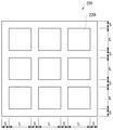
図2は、本実施形態に係る電力供給装置の概要構成を示す説明図である。図2(a)は、電力供給装置200の上面図を示し、図2(b)は、電力供給装置200の断面図を示し、図2(c)は、電力供給装置200の下面図を示す。図2(b)の断面図は、図2(c)におけるB−B断面を示す。
(Power supply device)
FIG. 2 is an explanatory diagram showing a schematic configuration of the power supply apparatus according to the present embodiment. 2A is a top view of the
図2(c)に示すように、電力供給装置200の下面には、複数の電極220a〜220iが基板210にアレイ状に配列されて設けられている。基板210は、たとえば比誘電率が4.9の誘電体により構成される。電力供給システムにおいて、電力供給装置200の下面は、電磁波伝搬装置100の上面に対向して配置され、電極220は、電磁波伝搬装置100の浸出領域140に染み出す電磁場の変化を受信する。各電極220は、正方形の形状を有し、隣接する電極220との距離がそれぞれ等しくなるように設けられる。各電極220の中心同士の間隔は、電磁波伝搬装置100における第1導体部110の開口の中心同士の間隔よりも大きく設定される。これにより、電力供給装置200は、電磁波伝搬装置100の狭間領域130において伝搬される電磁波のエネルギを効率よく取り出すことが可能となる。
As shown in FIG. 2C, a plurality of
複数の電極220は、基板210の下面において、2次元的に配列されることが好ましい。これにより、基板210の面積を効率よく利用することができる。各電極220の形状は異なってもよいが、正方形、正六角形など、同サイズの正多角形に形成することで、規則的に、たとえばマトリックス状に2次元配列することが可能となる。
The plurality of
図2(a)に示すように、電力供給装置200の上面には、2つの電極220で受信した電磁波を整流する複数の整流回路230が設けられる。具体的には、整流回路230aが、電極220aおよび電極220bと電気的に接続し、電極220aおよび電極220bで受信する電磁波を全波整流する。各電極220は、非共振型のアンテナに相当し、5GHz帯の電磁波、2.4GHz帯の電磁波や、950MHz帯の電磁波など、様々な周波数の電磁波を受信でき、また整流回路230は、入力波の正負にかかわらず、正出力を獲得できる。
As shown in FIG. 2A, a plurality of
同様に、整流回路230bが電極220bおよび電極220cと電気的に接続し、整流回路230cが電極220aおよび電極220dと電気的に接続し、整流回路230dが電極220bおよび電極220eと電気的に接続し、整流回路230eが電極220cおよび電極220fと電気的に接続し、整流回路230fが電極220dおよび電極220eと電気的に接続し、整流回路230gが電極220eおよび電極220fと電気的に接続し、整流回路230hが電極220dおよび電極220gと電気的に接続し、整流回路230iが電極220eおよび電極220hと電気的に接続し、整流回路230jが電極220fおよび電極220iと電気的に接続し、整流回路230kが電極220gおよび電極220hと電気的に接続し、整流回路230lが電極220hおよび電極220iと電気的に接続する。この例では、整流回路230が、隣り合う電極220同士を電気的に接続している。
Similarly, the
このように、電力供給装置200では、1つの電極220が、異なる2以上の整流回路230に接続される。図2(a)では、電極220a、220c、220g、220iが2つの整流回路230に接続され、また電極220b、220d、220f、220hが3つの整流回路230に接続され、電極220eが4つの整流回路230に接続される。このように、電極220を、複数の整流回路230の入力として共用することにより、効率的に電磁波エネルギを取り出すことが可能となり、基板210の下面スペースを有効に利用できる。また、電極220を複数の整流回路230の入力として共用することで、結果として、整流回路230の数を、電極220の数よりも多くすることができる。たとえば、整流回路230の出力を並列接続することで、それぞれの整流回路230の出力を加算した大きな電力を取り出すことができるが、整流回路230の数を電極220の数よりも多くすることで、電力を効率よく取り出す電力供給システム10を実現することが可能となる。
Thus, in the
図2(b)に示すように、基板210には電極220と、整流回路230の接点240とを電気的に接続するビアが形成される。各整流回路230は、接点240aおよび接点240bを有し、それぞれの接点240は、異なる電極220と電気的に接続される。
As shown in FIG. 2B, vias that electrically connect the
図3(a)は、整流回路230の回路構成を示す。整流回路230は、既知の全波整流回路として構成されてよい。整流回路230は、ダイオードブリッジと平滑化コンデンサにより構成される。整流回路230は、電極220との接点240a、240bを有し、また2つの出力端子242a、242bを備える。
FIG. 3A shows a circuit configuration of the
図3(b)は、基板210の上面における接点240の配置を示す。図中、黒丸は接点240aを示し、白丸は接点240bを示す。なお、この接点240の配置は例示であり、いずれの配置をとる場合であっても、整流回路230が、異なる電極220からの電磁波を受信できる構成になっていればよい。
FIG. 3B shows the arrangement of the contacts 240 on the upper surface of the
(電力供給システム)
図4は、電力を負荷に供給する電力供給システムを示す。電力供給システム10は、電磁波伝搬装置100の上面に電力供給装置200を載置することで実現される。電力供給装置200は、電磁波伝搬装置100上面の任意の位置に載置されてよい。
(Power supply system)
FIG. 4 shows a power supply system that supplies power to a load. The
電磁波伝搬装置100は、導電層150、誘電層160、メッシュ層170および絶縁層180により構成されるシート状の積層構造をとり、メッシュ層170と導電層150に印加される電磁波を誘電層160において伝搬させる。ここで導電層150は、図1(b)における第2導体部120に対応し、誘電層160は、狭間領域130に対応し、またメッシュ層170は、第1導体部110が設けられた層に対応する。
The electromagnetic
既述したように、電磁波伝搬装置100では、メッシュ層170と導電層150に電磁波が印加されると、電磁場は浸出領域140まで染み出す特性をもつ。したがって、第1導体部110の開口上面に伝搬する電磁波が電極220により受信されるように、絶縁層180の厚みは、浸出領域140の最大高さよりも薄くされる必要がある。なお絶縁層180は、電磁波伝搬装置100ではなく、電力供給装置200の下面に設けられてもよい。また、絶縁層180は電磁波伝搬装置100または電力供給装置200に設けられなくてもよく、メッシュ層170上に紙などの絶縁物を置き、その上に電力供給装置200を載置することで、メッシュ層170と電極220との導通を回避してもよい。
As described above, in the electromagnetic
図示されるように、電力供給装置200の複数の電極220は基板210の下面に設けられ、電磁波伝搬装置100の表面、具体的にはメッシュ層170の表面に対して平面上に配列される。すなわち複数の電極220は、電磁波伝搬装置100の表面に対して実質的に同じ高さの位置に配置される。これにより、全ての電極220が、電磁波伝搬装置100から略均等に電磁波を受信できるようになる。
As illustrated, the plurality of
結合部250は、複数の整流回路230の出力を結合して、負荷300に電力を供給する。結合部250は、各整流回路230の出力端子242を直列接続してもよく、また並列接続してもよい。図4では、結合部250が、各整流回路230の出力端子242を並列接続し、各整流回路230から出力される電流を加算して負荷300に供給している。このように、電力供給システム10では、複数の整流回路230の出力を加算することで、大きな電力を取り出すことが可能となる。1つの電極220を複数の整流回路230で共用することで、基板210の下面スペースを有効利用することができ、電力供給装置200を小型化できるという利点もある。
The
負荷300は、電磁波伝搬装置100を信号伝達装置として作用させたときに、インターフェース装置を介して接続される外部の通信装置、各種の通信素子、通信回路、センサ、RFタグ、アクチュエータなどであってよい。また負荷300はバッテリであって、電力供給システム10がバッテリ充電に利用されてもよい。
The
電力供給装置200は、持ち運び可能に構成され、電磁波伝搬装置100上の任意の位置に載置されてよい。1つの電力供給装置200により取得できる電力は、印加される電磁波により決定されるが、必要量の電力を得るために、複数の電力供給装置200を電磁波伝搬装置100上に載置して、電力供給装置200の出力を並列接続することで電力を取り出すことも可能である。このように、電力供給装置200を持ち運び可能に構成して、任意数の電力供給装置200を接続して電磁波伝搬装置100に載置することで、必要量の電力を容易に生成することが可能となり、たとえば生成した電力を予めバッテリに蓄積しておくことで、信号伝達システムを効率的に動作させることが可能となる。
The
また、電力供給システム10として動作するとき、電磁波伝搬装置100には、電力供給用の電磁波が印加されてもよい。また、信号伝達システムとしての動作中に、電力供給装置200がその有意な信号を伝搬する電磁波を受信して、電力を生成してもよい。
When operating as the
(動作実験)
本発明者は、本実施形態の電力供給システム10の電力供給特性についての実験を行った。
図5は、電磁波伝搬装置100に電磁波を印加するときに使用されるSMAコネクタを示す。図中に示す数字は、SMAコネクタ400の寸法(単位mm)を示し、形状は軸対称である。SMAコネクタ400は、共振型のコネクタであり、外部発振器を接続して、電磁波伝搬装置100に所定の周波数の電磁波を印加する。
(Operation experiment)
The inventor conducted experiments on the power supply characteristics of the
FIG. 5 shows an SMA connector used when an electromagnetic wave is applied to the electromagnetic
図6は、電極220のアレイ形状を示し、実験では電極220のサイズLを変化させる。具体的にLを、10mm、20mm、30mmと変化させて、電力供給システム10の電力供給特性について実験した。なお、電極220の間隔は5mmに設定した。
FIG. 6 shows an array shape of the
図7は、電力供給システム10の実験環境を示す。第1導体部110の線幅(メッシュ線幅)は1mm、正方形の開口の一辺長さは7mm、電磁波伝搬装置100のシート形状は長さ800mm×幅500mmとした。また、SMAコネクタ400の中心をシート左端から150mm、幅中央位置(下端から250mm)の地点に配置し、また電力供給装置200の左端を、シート左端から650mm、その中心が幅中央位置にくるように配置した。
FIG. 7 shows an experimental environment of the
なお、電磁波伝搬装置100の厚さは2mm、メッシュ層170を構成する第1導体部110は、厚さ30μmのアルミニウムで形成する。誘電層160の比誘電率は1.4、導電層150を構成する第2導体部120は、厚さ30μmのアルミニウムで形成する。メッシュ層170の上面には、75μmの絶縁フィルムを配置する。以上の条件のもと、電力供給装置200の電極長さLを10mm、20mm、30mmと変化させて、取得電力を測定した。
The electromagnetic
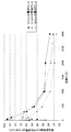
図8は、単位面積当たりの取得電力Pを示す実験結果である。SMAコネクタ400には、出力10Wの2.35GHz発振器を接続した。実験では、電力供給装置200における全ての整流回路230からの出力端子242を結合部250において並列接続し、結合部250における出力端子間に負荷300[Ω]を接続し、負荷300の両端に発生する電圧値を計測して電力を求め、電極220の総面積から単位面積当たりの取得電力Pを求めた。
FIG. 8 is an experimental result showing the acquired power P per unit area. To the
以上の実験結果により、電力供給装置200を電磁波伝搬装置100に載置することで、電力を負荷300に供給できることが確認された。また、図8に示す実験結果より、電極220が小さい方が、単位面積当たりの取得電力が高いことも確認された。そのため、電力供給装置200においては、電極220を小さく形成し、基板210上に形成する電極220の数を多くすることで、取得できる電力量を大きくすることが分かった。
From the above experimental results, it was confirmed that the power can be supplied to the
以上、本発明を実施例をもとに説明した。これらの実施例は例示であり、それらの各構成要素や各処理プロセスの組合せにいろいろな変形例が可能なこと、またそうした変形例も本発明の範囲にあることは当業者に理解されるところである。 In the above, this invention was demonstrated based on the Example. These embodiments are exemplifications, and it is understood by those skilled in the art that various modifications can be made to the combination of each component and each processing process, and such modifications are within the scope of the present invention. is there.
10・・・電力供給システム、100・・・電磁波伝搬装置、110・・・第1導体部、120・・・第2導体部、130・・・狭間領域、140・・・浸出領域、150・・・導電層、160・・・誘電層、170・・・メッシュ層、180・・・絶縁層、200・・・電力供給装置、210・・・基板、220・・・電極、230・・・整流回路、240・・・接点、242・・・出力端子、250・・・結合部、300・・・負荷、400・・・SMAコネクタ。
DESCRIPTION OF
Claims (8)
電磁波を伝搬する電磁波伝搬装置と、
負荷に電力を供給する電力供給装置とを備え、
前記電力供給装置は、
前記電磁波伝搬装置の表面に近接して配置される基板と、
前記基板においてマトリックス状に配列され、前記電磁波伝搬装置の表面に対して実質的に同じ高さの位置に配置されて、前記電磁波伝搬装置により伝搬される電磁波を受信する複数の電極と、
隣り合う2つの電極の間の電圧を整流する複数の整流回路と、
複数の整流回路の出力を結合する結合部と、
を有することを特徴とする電力供給システム。 A power supply system,
An electromagnetic wave propagation device for propagating electromagnetic waves;
A power supply device for supplying power to the load,
The power supply device
A substrate disposed in proximity to the surface of the electromagnetic wave propagation device;
A plurality of electrodes arranged in a matrix on the substrate, arranged at substantially the same height relative to the surface of the electromagnetic wave propagation device, and receiving electromagnetic waves propagated by the electromagnetic wave propagation device;
A plurality of rectifier circuits for rectifying a voltage between two adjacent electrodes;
A coupling unit that couples outputs of a plurality of rectifier circuits;
A power supply system comprising:
電極の中心同士の間隔は、第1導体部の開口の中心同士の間隔よりも大きく設定されていることを特徴とする請求項1から3のいずれかに記載の電力供給システム。 The electromagnetic wave propagation device includes a first conductor part having a plurality of openings, a second conductor part substantially parallel to the first conductor part, and a dielectric layer between the first conductor part and the second conductor part,
4. The power supply system according to claim 1, wherein an interval between the centers of the electrodes is set larger than an interval between the centers of the openings of the first conductor portion. 5.
電磁波を受信する複数の電極と、
隣り合う2つの電極の間の電圧を整流する複数の整流回路と、
マトリックス状に配列された複数の電極を下面に支持し、複数の整流回路を上面に支持して、電極と整流回路とを電気的に接続する基板と、
複数の整流回路の出力を結合する結合部と、
を備えることを特徴とする電力供給装置。 A power supply device for supplying power to a load,
A plurality of electrodes for receiving electromagnetic waves;
A plurality of rectifier circuits for rectifying a voltage between two adjacent electrodes;
A substrate that supports a plurality of electrodes arranged in a matrix on the lower surface, supports a plurality of rectifier circuits on the upper surface, and electrically connects the electrodes and the rectifier circuit;
A coupling unit that couples outputs of a plurality of rectifier circuits;
A power supply device comprising:
Priority Applications (1)
| Application Number | Priority Date | Filing Date | Title |
|---|---|---|---|
| JP2007137250A JP4768670B2 (en) | 2007-05-23 | 2007-05-23 | Power supply system and power supply device |
Applications Claiming Priority (1)
| Application Number | Priority Date | Filing Date | Title |
|---|---|---|---|
| JP2007137250A JP4768670B2 (en) | 2007-05-23 | 2007-05-23 | Power supply system and power supply device |
Publications (3)
| Publication Number | Publication Date |
|---|---|
| JP2008295176A JP2008295176A (en) | 2008-12-04 |
| JP2008295176A5 JP2008295176A5 (en) | 2010-07-01 |
| JP4768670B2 true JP4768670B2 (en) | 2011-09-07 |
Family
ID=40169347
Family Applications (1)
| Application Number | Title | Priority Date | Filing Date |
|---|---|---|---|
| JP2007137250A Active JP4768670B2 (en) | 2007-05-23 | 2007-05-23 | Power supply system and power supply device |
Country Status (1)
| Country | Link |
|---|---|
| JP (1) | JP4768670B2 (en) |
Cited By (1)
| Publication number | Priority date | Publication date | Assignee | Title |
|---|---|---|---|---|
| US11682925B2 (en) | 2020-12-28 | 2023-06-20 | University-Industry Cooperation Group Of Kyung Hee University | Wireless power transmission apparatus for minimizing magnetic field exposure based on cavity resonance |
Families Citing this family (16)
| Publication number | Priority date | Publication date | Assignee | Title |
|---|---|---|---|---|
| JP2009055379A (en) | 2007-08-27 | 2009-03-12 | National Institute Of Information & Communication Technology | Communication device and two-dimensional communication system using the same |
| JPWO2010131612A1 (en) | 2009-05-14 | 2012-11-01 | 日本電気株式会社 | Surface communication device |
| JP5368193B2 (en) * | 2009-07-03 | 2013-12-18 | 帝人株式会社 | Communication sheet structure |
| JP5515562B2 (en) * | 2009-09-28 | 2014-06-11 | Tdk株式会社 | Wireless power receiving apparatus and wireless power transmission system |
| WO2011052361A1 (en) * | 2009-10-30 | 2011-05-05 | 日本電気株式会社 | Surface communication device |
| JP5605153B2 (en) | 2010-10-15 | 2014-10-15 | ソニー株式会社 | Power supply device, power supply method, and power supply system |
| WO2013124935A1 (en) * | 2012-02-24 | 2013-08-29 | 日本電気株式会社 | Power receiving device, power supplying device, and communication device |
| US11502551B2 (en) | 2012-07-06 | 2022-11-15 | Energous Corporation | Wirelessly charging multiple wireless-power receivers using different subsets of an antenna array to focus energy at different locations |
| US10256657B2 (en) * | 2015-12-24 | 2019-04-09 | Energous Corporation | Antenna having coaxial structure for near field wireless power charging |
| DE102014219679A1 (en) * | 2014-09-29 | 2016-03-31 | Fraunhofer-Gesellschaft zur Förderung der angewandten Forschung e.V. | ENERGY SUPPLY DEVICE, CHARGING STATION, TABLE TOP, WALL CLADDING AND SYSTEM |
| US10079515B2 (en) | 2016-12-12 | 2018-09-18 | Energous Corporation | Near-field RF charging pad with multi-band antenna element with adaptive loading to efficiently charge an electronic device at any position on the pad |
| CN108702018B (en) * | 2015-12-24 | 2022-01-18 | 艾诺格思公司 | System and method for wireless charging by multiple receiving devices |
| US11863001B2 (en) | 2015-12-24 | 2024-01-02 | Energous Corporation | Near-field antenna for wireless power transmission with antenna elements that follow meandering patterns |
| US12074460B2 (en) | 2017-05-16 | 2024-08-27 | Wireless Electrical Grid Lan, Wigl Inc. | Rechargeable wireless power bank and method of using |
| US11462949B2 (en) | 2017-05-16 | 2022-10-04 | Wireless electrical Grid LAN, WiGL Inc | Wireless charging method and system |
| US11018779B2 (en) | 2019-02-06 | 2021-05-25 | Energous Corporation | Systems and methods of estimating optimal phases to use for individual antennas in an antenna array |
-
2007
- 2007-05-23 JP JP2007137250A patent/JP4768670B2/en active Active
Cited By (1)
| Publication number | Priority date | Publication date | Assignee | Title |
|---|---|---|---|---|
| US11682925B2 (en) | 2020-12-28 | 2023-06-20 | University-Industry Cooperation Group Of Kyung Hee University | Wireless power transmission apparatus for minimizing magnetic field exposure based on cavity resonance |
Also Published As
| Publication number | Publication date |
|---|---|
| JP2008295176A (en) | 2008-12-04 |
Similar Documents
| Publication | Publication Date | Title |
|---|---|---|
| JP4768670B2 (en) | Power supply system and power supply device | |
| JP4538594B2 (en) | Signal transmission system | |
| JP4650906B2 (en) | Signal transmission device, interface device, and communication system | |
| CN108199151A (en) | A kind of energy information parallel transmission rectenna array | |
| JP2008295176A5 (en) | ||
| JP2007281678A (en) | Signal transmission system | |
| KR20110035196A (en) | Spiral antenna and wireless power transmission device using spiral antenna | |
| CN105308828A (en) | Power transmitter, power supply device, power consumption device, power supply system and method for producing power transmitter | |
| US9801307B2 (en) | Capacitor module for a mobile working machine | |
| JP6642783B2 (en) | Transmission line equipment | |
| CN109478721A (en) | The C feed antennas being formed on multilayer board edge | |
| CN109121285A (en) | A kind of board structure of circuit and electronic equipment | |
| CN107068251A (en) | Isolated bus, the manufacture method of isolated bus and electronic equipment | |
| JP2010063213A (en) | Power receiver and power transmitting system | |
| CN103733741A (en) | High-frequency signal line and electronic device | |
| CN105578740B (en) | Single side Rigid Flex and mobile terminal | |
| Freychet et al. | Analytical optimization of piezoelectric acoustic power transfer systems | |
| CN103733426A (en) | High-frequency signal line and electronic device | |
| JP2010056952A (en) | Electromagnetic wave transfer medium system and method for connecting electromagnetic wave transfer medium | |
| WO2015108094A1 (en) | Signal line | |
| CN105636351B (en) | Flexible circuit board and mobile terminal | |
| JP5868658B2 (en) | Structure | |
| CN102759644B (en) | Cantilever type high-frequency probe card | |
| Malik et al. | Flexible rectennas for wireless power transfer to wearable sensors at 24 GHz | |
| Yang et al. | Wireless power transmission using dipole rectennas made on flexible cellulose membrane |
Legal Events
| Date | Code | Title | Description |
|---|---|---|---|
| A521 | Request for written amendment filed |
Free format text: JAPANESE INTERMEDIATE CODE: A523 Effective date: 20100427 |
|
| A621 | Written request for application examination |
Free format text: JAPANESE INTERMEDIATE CODE: A621 Effective date: 20100427 |
|
| A977 | Report on retrieval |
Free format text: JAPANESE INTERMEDIATE CODE: A971007 Effective date: 20110602 |
|
| TRDD | Decision of grant or rejection written | ||
| A01 | Written decision to grant a patent or to grant a registration (utility model) |
Free format text: JAPANESE INTERMEDIATE CODE: A01 Effective date: 20110614 |
|
| A01 | Written decision to grant a patent or to grant a registration (utility model) |
Free format text: JAPANESE INTERMEDIATE CODE: A01 |
|
| A61 | First payment of annual fees (during grant procedure) |
Free format text: JAPANESE INTERMEDIATE CODE: A61 Effective date: 20110616 |
|
| R150 | Certificate of patent or registration of utility model |
Ref document number: 4768670 Country of ref document: JP Free format text: JAPANESE INTERMEDIATE CODE: R150 Free format text: JAPANESE INTERMEDIATE CODE: R150 |
|
| FPAY | Renewal fee payment (event date is renewal date of database) |
Free format text: PAYMENT UNTIL: 20140624 Year of fee payment: 3 |
|
| S531 | Written request for registration of change of domicile |
Free format text: JAPANESE INTERMEDIATE CODE: R313531 |
|
| R350 | Written notification of registration of transfer |
Free format text: JAPANESE INTERMEDIATE CODE: R350 |
|
| R250 | Receipt of annual fees |
Free format text: JAPANESE INTERMEDIATE CODE: R250 |
|
| R250 | Receipt of annual fees |
Free format text: JAPANESE INTERMEDIATE CODE: R250 |
|
| R250 | Receipt of annual fees |
Free format text: JAPANESE INTERMEDIATE CODE: R250 |
|
| R250 | Receipt of annual fees |
Free format text: JAPANESE INTERMEDIATE CODE: R250 |
|
| R250 | Receipt of annual fees |
Free format text: JAPANESE INTERMEDIATE CODE: R250 |
|
| R250 | Receipt of annual fees |
Free format text: JAPANESE INTERMEDIATE CODE: R250 |
|
| R250 | Receipt of annual fees |
Free format text: JAPANESE INTERMEDIATE CODE: R250 |
|
| R250 | Receipt of annual fees |
Free format text: JAPANESE INTERMEDIATE CODE: R250 |
|
| R250 | Receipt of annual fees |
Free format text: JAPANESE INTERMEDIATE CODE: R250 |
|
| R250 | Receipt of annual fees |
Free format text: JAPANESE INTERMEDIATE CODE: R250 |
|
| R250 | Receipt of annual fees |
Free format text: JAPANESE INTERMEDIATE CODE: R250 |