JP4764962B2 - Surface illumination light source device and surface illumination device - Google Patents
Surface illumination light source device and surface illumination device Download PDFInfo
- Publication number
- JP4764962B2 JP4764962B2 JP2007164796A JP2007164796A JP4764962B2 JP 4764962 B2 JP4764962 B2 JP 4764962B2 JP 2007164796 A JP2007164796 A JP 2007164796A JP 2007164796 A JP2007164796 A JP 2007164796A JP 4764962 B2 JP4764962 B2 JP 4764962B2
- Authority
- JP
- Japan
- Prior art keywords
- light source
- radiation
- light
- opening
- source device
- Prior art date
- Legal status (The legal status is an assumption and is not a legal conclusion. Google has not performed a legal analysis and makes no representation as to the accuracy of the status listed.)
- Expired - Fee Related
Links
- 238000005286 illumination Methods 0.000 title claims description 63
- 230000005855 radiation Effects 0.000 claims description 91
- 239000000463 material Substances 0.000 claims description 6
- 230000001902 propagating effect Effects 0.000 claims description 6
- 230000014509 gene expression Effects 0.000 claims description 3
- 238000010586 diagram Methods 0.000 description 4
- 230000002093 peripheral effect Effects 0.000 description 3
- 238000009792 diffusion process Methods 0.000 description 2
- 229920003023 plastic Polymers 0.000 description 2
- 239000004925 Acrylic resin Substances 0.000 description 1
- 229920000178 Acrylic resin Polymers 0.000 description 1
- GWEVSGVZZGPLCZ-UHFFFAOYSA-N Titan oxide Chemical compound O=[Ti]=O GWEVSGVZZGPLCZ-UHFFFAOYSA-N 0.000 description 1
- 230000005540 biological transmission Effects 0.000 description 1
- 230000007423 decrease Effects 0.000 description 1
- 238000002474 experimental method Methods 0.000 description 1
- 239000010419 fine particle Substances 0.000 description 1
- NBVXSUQYWXRMNV-UHFFFAOYSA-N fluoromethane Chemical compound FC NBVXSUQYWXRMNV-UHFFFAOYSA-N 0.000 description 1
- 230000004907 flux Effects 0.000 description 1
- 238000005187 foaming Methods 0.000 description 1
- 230000020169 heat generation Effects 0.000 description 1
- 230000031700 light absorption Effects 0.000 description 1
- 239000007788 liquid Substances 0.000 description 1
- 239000011159 matrix material Substances 0.000 description 1
- 229910052751 metal Inorganic materials 0.000 description 1
- 239000002184 metal Substances 0.000 description 1
- 239000011859 microparticle Substances 0.000 description 1
- 239000005304 optical glass Substances 0.000 description 1
- 230000000149 penetrating effect Effects 0.000 description 1
- 239000004033 plastic Substances 0.000 description 1
- -1 polytetrafluoroethylene Polymers 0.000 description 1
- 229920001343 polytetrafluoroethylene Polymers 0.000 description 1
- 239000004810 polytetrafluoroethylene Substances 0.000 description 1
- 239000011148 porous material Substances 0.000 description 1
- 229920002050 silicone resin Polymers 0.000 description 1
- 229920003002 synthetic resin Polymers 0.000 description 1
- 239000000057 synthetic resin Substances 0.000 description 1
- 235000010215 titanium dioxide Nutrition 0.000 description 1
Images


Classifications
-
- F—MECHANICAL ENGINEERING; LIGHTING; HEATING; WEAPONS; BLASTING
- F21—LIGHTING
- F21V—FUNCTIONAL FEATURES OR DETAILS OF LIGHTING DEVICES OR SYSTEMS THEREOF; STRUCTURAL COMBINATIONS OF LIGHTING DEVICES WITH OTHER ARTICLES, NOT OTHERWISE PROVIDED FOR
- F21V13/00—Producing particular characteristics or distribution of the light emitted by means of a combination of elements specified in two or more of main groups F21V1/00 - F21V11/00
- F21V13/02—Combinations of only two kinds of elements
-
- G—PHYSICS
- G02—OPTICS
- G02F—OPTICAL DEVICES OR ARRANGEMENTS FOR THE CONTROL OF LIGHT BY MODIFICATION OF THE OPTICAL PROPERTIES OF THE MEDIA OF THE ELEMENTS INVOLVED THEREIN; NON-LINEAR OPTICS; FREQUENCY-CHANGING OF LIGHT; OPTICAL LOGIC ELEMENTS; OPTICAL ANALOGUE/DIGITAL CONVERTERS
- G02F1/00—Devices or arrangements for the control of the intensity, colour, phase, polarisation or direction of light arriving from an independent light source, e.g. switching, gating or modulating; Non-linear optics
- G02F1/01—Devices or arrangements for the control of the intensity, colour, phase, polarisation or direction of light arriving from an independent light source, e.g. switching, gating or modulating; Non-linear optics for the control of the intensity, phase, polarisation or colour
- G02F1/13—Devices or arrangements for the control of the intensity, colour, phase, polarisation or direction of light arriving from an independent light source, e.g. switching, gating or modulating; Non-linear optics for the control of the intensity, phase, polarisation or colour based on liquid crystals, e.g. single liquid crystal display cells
- G02F1/133—Constructional arrangements; Operation of liquid crystal cells; Circuit arrangements
- G02F1/1333—Constructional arrangements; Manufacturing methods
- G02F1/1335—Structural association of cells with optical devices, e.g. polarisers or reflectors
- G02F1/1336—Illuminating devices
- G02F1/133602—Direct backlight
- G02F1/133605—Direct backlight including specially adapted reflectors
-
- G—PHYSICS
- G02—OPTICS
- G02B—OPTICAL ELEMENTS, SYSTEMS OR APPARATUS
- G02B6/00—Light guides; Structural details of arrangements comprising light guides and other optical elements, e.g. couplings
- G02B6/0001—Light guides; Structural details of arrangements comprising light guides and other optical elements, e.g. couplings specially adapted for lighting devices or systems
- G02B6/0011—Light guides; Structural details of arrangements comprising light guides and other optical elements, e.g. couplings specially adapted for lighting devices or systems the light guides being planar or of plate-like form
- G02B6/0033—Means for improving the coupling-out of light from the light guide
- G02B6/005—Means for improving the coupling-out of light from the light guide provided by one optical element, or plurality thereof, placed on the light output side of the light guide
- G02B6/0055—Reflecting element, sheet or layer
-
- G—PHYSICS
- G02—OPTICS
- G02F—OPTICAL DEVICES OR ARRANGEMENTS FOR THE CONTROL OF LIGHT BY MODIFICATION OF THE OPTICAL PROPERTIES OF THE MEDIA OF THE ELEMENTS INVOLVED THEREIN; NON-LINEAR OPTICS; FREQUENCY-CHANGING OF LIGHT; OPTICAL LOGIC ELEMENTS; OPTICAL ANALOGUE/DIGITAL CONVERTERS
- G02F1/00—Devices or arrangements for the control of the intensity, colour, phase, polarisation or direction of light arriving from an independent light source, e.g. switching, gating or modulating; Non-linear optics
- G02F1/01—Devices or arrangements for the control of the intensity, colour, phase, polarisation or direction of light arriving from an independent light source, e.g. switching, gating or modulating; Non-linear optics for the control of the intensity, phase, polarisation or colour
- G02F1/13—Devices or arrangements for the control of the intensity, colour, phase, polarisation or direction of light arriving from an independent light source, e.g. switching, gating or modulating; Non-linear optics for the control of the intensity, phase, polarisation or colour based on liquid crystals, e.g. single liquid crystal display cells
- G02F1/133—Constructional arrangements; Operation of liquid crystal cells; Circuit arrangements
- G02F1/1333—Constructional arrangements; Manufacturing methods
- G02F1/1335—Structural association of cells with optical devices, e.g. polarisers or reflectors
- G02F1/1336—Illuminating devices
- G02F1/133602—Direct backlight
- G02F1/133603—Direct backlight with LEDs
-
- G—PHYSICS
- G09—EDUCATION; CRYPTOGRAPHY; DISPLAY; ADVERTISING; SEALS
- G09F—DISPLAYING; ADVERTISING; SIGNS; LABELS OR NAME-PLATES; SEALS
- G09F13/00—Illuminated signs; Luminous advertising
- G09F13/20—Illuminated signs; Luminous advertising with luminescent surfaces or parts
- G09F13/22—Illuminated signs; Luminous advertising with luminescent surfaces or parts electroluminescent
-
- F—MECHANICAL ENGINEERING; LIGHTING; HEATING; WEAPONS; BLASTING
- F21—LIGHTING
- F21Y—INDEXING SCHEME ASSOCIATED WITH SUBCLASSES F21K, F21L, F21S and F21V, RELATING TO THE FORM OR THE KIND OF THE LIGHT SOURCES OR OF THE COLOUR OF THE LIGHT EMITTED
- F21Y2105/00—Planar light sources
- F21Y2105/10—Planar light sources comprising a two-dimensional array of point-like light-generating elements
-
- F—MECHANICAL ENGINEERING; LIGHTING; HEATING; WEAPONS; BLASTING
- F21—LIGHTING
- F21Y—INDEXING SCHEME ASSOCIATED WITH SUBCLASSES F21K, F21L, F21S and F21V, RELATING TO THE FORM OR THE KIND OF THE LIGHT SOURCES OR OF THE COLOUR OF THE LIGHT EMITTED
- F21Y2115/00—Light-generating elements of semiconductor light sources
- F21Y2115/10—Light-emitting diodes [LED]
-
- G—PHYSICS
- G02—OPTICS
- G02B—OPTICAL ELEMENTS, SYSTEMS OR APPARATUS
- G02B6/00—Light guides; Structural details of arrangements comprising light guides and other optical elements, e.g. couplings
- G02B6/0001—Light guides; Structural details of arrangements comprising light guides and other optical elements, e.g. couplings specially adapted for lighting devices or systems
- G02B6/0011—Light guides; Structural details of arrangements comprising light guides and other optical elements, e.g. couplings specially adapted for lighting devices or systems the light guides being planar or of plate-like form
- G02B6/0033—Means for improving the coupling-out of light from the light guide
- G02B6/0058—Means for improving the coupling-out of light from the light guide varying in density, size, shape or depth along the light guide
- G02B6/0061—Means for improving the coupling-out of light from the light guide varying in density, size, shape or depth along the light guide to provide homogeneous light output intensity
-
- G—PHYSICS
- G02—OPTICS
- G02F—OPTICAL DEVICES OR ARRANGEMENTS FOR THE CONTROL OF LIGHT BY MODIFICATION OF THE OPTICAL PROPERTIES OF THE MEDIA OF THE ELEMENTS INVOLVED THEREIN; NON-LINEAR OPTICS; FREQUENCY-CHANGING OF LIGHT; OPTICAL LOGIC ELEMENTS; OPTICAL ANALOGUE/DIGITAL CONVERTERS
- G02F1/00—Devices or arrangements for the control of the intensity, colour, phase, polarisation or direction of light arriving from an independent light source, e.g. switching, gating or modulating; Non-linear optics
- G02F1/01—Devices or arrangements for the control of the intensity, colour, phase, polarisation or direction of light arriving from an independent light source, e.g. switching, gating or modulating; Non-linear optics for the control of the intensity, phase, polarisation or colour
- G02F1/13—Devices or arrangements for the control of the intensity, colour, phase, polarisation or direction of light arriving from an independent light source, e.g. switching, gating or modulating; Non-linear optics for the control of the intensity, phase, polarisation or colour based on liquid crystals, e.g. single liquid crystal display cells
- G02F1/133—Constructional arrangements; Operation of liquid crystal cells; Circuit arrangements
- G02F1/1333—Constructional arrangements; Manufacturing methods
- G02F1/1335—Structural association of cells with optical devices, e.g. polarisers or reflectors
- G02F1/1336—Illuminating devices
- G02F1/133602—Direct backlight
- G02F1/133611—Direct backlight including means for improving the brightness uniformity
-
- Y—GENERAL TAGGING OF NEW TECHNOLOGICAL DEVELOPMENTS; GENERAL TAGGING OF CROSS-SECTIONAL TECHNOLOGIES SPANNING OVER SEVERAL SECTIONS OF THE IPC; TECHNICAL SUBJECTS COVERED BY FORMER USPC CROSS-REFERENCE ART COLLECTIONS [XRACs] AND DIGESTS
- Y10—TECHNICAL SUBJECTS COVERED BY FORMER USPC
- Y10S—TECHNICAL SUBJECTS COVERED BY FORMER USPC CROSS-REFERENCE ART COLLECTIONS [XRACs] AND DIGESTS
- Y10S362/00—Illumination
- Y10S362/80—Light emitting diode
Description
本発明は、LCDバックライト、照明用看板、照明灯、各種車両等の表示装置に用いられる面照明光源装置及び面照明装置に関する。 The present invention relates to a surface illumination light source device and a surface illumination device used for display devices such as LCD backlights, lighting signs, illumination lamps, and various vehicles.
従来から、表示装置や照明等の光源として、電力消費量や発熱が少ない点から発光ダイオード(LED)の使用が検討されているが、LEDは指向性が強いため、広い面で均一光量分布を得るためには、種々の工夫が必要とされている。 Conventionally, the use of light-emitting diodes (LEDs) as a light source for display devices and lighting has been studied from the viewpoint of low power consumption and heat generation. However, because LEDs are highly directional, they have a uniform light distribution over a wide area. In order to obtain, various devices are required.
例えば特許文献1には、光源から発せられた光が入射する光入射端面及び導光される光が出射する光出射面を有する導光体を備え、この導光体に形成された局所的レンズ列を、光入射端面に入射した光のうちの最大強度光の入射位置での輝度分布におけるピーク光の方向と異なる方向に形成して、輝度不均一を解消する点が開示されている。 For example, Patent Document 1 includes a light guide having a light incident end face on which light emitted from a light source is incident and a light exit surface on which light guided is emitted, and a local lens formed on the light guide. It is disclosed that the non-uniform luminance is eliminated by forming the columns in a direction different from the direction of the peak light in the luminance distribution at the incident position of the maximum intensity light among the light incident on the light incident end face.
また、特許文献2には、一端に開口部が形成され、その内側壁が光の反射面である光源収容部を有するランプハウジングと、光源収容部に設けられた発光ダイオードと、開口部の前面に設けられた表示板とを備え、発光ダイオードからの光を拡散反射して均一にした点が開示されている。 In Patent Document 2, an opening is formed at one end, a lamp housing having a light source housing portion whose inner wall is a light reflecting surface, a light emitting diode provided in the light source housing portion, and a front surface of the opening portion. And a display panel provided in the above, and the light from the light emitting diode is diffusely reflected and made uniform.
さらに、特許文献3では、光の放射面上に形成された拡散層における微小反射部からの反射光と、発光ダイオードの周辺に設けられた反射器と、の間での反射の繰り返しにより、均一光を得る旨が開示されている。 Furthermore, in Patent Document 3, the light is uniformly reflected by the reflection between the reflected light from the minute reflecting portion in the diffusion layer formed on the light emitting surface and the reflector provided around the light emitting diode. It is disclosed that light is obtained.
また、特許文献4では、LEDから出射された指向性のある光(特にLED直上の強い光)を、放射面に形成された反射部でLED側に反射させ、これにより、光の方向を変化させてLEDからの光強度を減少させ、均一な光を得る点が開示されている。
しかしながら、特許文献1では、LEDによる指向性の強い光を均等化するために、LED光源を放射方向に対して横に設けたりしている。このため、大きなスペースを必要とする。 However, in patent document 1, in order to equalize the light with strong directivity by LED, the LED light source is provided laterally with respect to the radiation direction. For this reason, a large space is required.
また、特許文献2では、LEDの放射方向に所定の厚みが必要となる。また、内側拡散フィルムで散乱された光は、ベース板で吸収されてしまう等、LEDからの光を全て利用するとの思想は有さない。 Moreover, in patent document 2, predetermined | prescribed thickness is needed for the radiation | emission direction of LED. In addition, there is no idea that the light scattered by the inner diffusion film is absorbed by the base plate and all the light from the LED is used.
さらに、特許文献3では、放射面やLEDの周辺の底面には反射板が設けられていても、側面には反射板が設けられていない。このため、LEDを取り囲むような空間において、光の多重反射を起こさせて全てのLEDからの光を利用しつつ均一な照明光を得ることはできない。 Furthermore, in Patent Document 3, even if a reflecting plate is provided on the radiation surface or the bottom surface around the LED, no reflecting plate is provided on the side surface. For this reason, in a space surrounding the LEDs, it is impossible to obtain uniform illumination light while causing multiple reflections of light and utilizing light from all the LEDs.
また、特許文献4では、LEDからの光の進行経路をコントロールすることで、均一な
照明を得ようとするものであり、放射面上の反射部は光の進行方向を変えるために用いられている。しかし、これでは光強度が弱められてしまうとともに、多重反射を利用して均一な光を得ることはできない。
Moreover, in patent document 4, it is trying to obtain uniform illumination by controlling the traveling path of the light from the LED, and the reflection part on the radiation surface is used to change the traveling direction of the light. Yes. However, this weakens the light intensity, and uniform light cannot be obtained using multiple reflection.
本発明は、斯かる課題を解決するためになされたもので、光源からの光を高い効率で利用しながら、光の放射方向の厚みを増大させることなく、放射面から所定の距離離れた面において均一な照明光を得ることのできる面照明光源装置及び面照明装置を提供することを目的とする。 The present invention has been made in order to solve such a problem, and uses the light from the light source with high efficiency, and without increasing the thickness of the light in the radiation direction, the surface away from the radiation surface by a predetermined distance. An object of the present invention is to provide a surface illumination light source device and a surface illumination device capable of obtaining uniform illumination light.
前記目的を達成するため、請求項1に係る発明は、
光を放射する点光源単体又は複数の点光源の集合体からなる一群の光源と、
該光源からの光を伝搬してその放射方向の所定位置に放射面を有する光学的に透明な導光体と、
該導光体の前記放射面以外の面を閉鎖し、光を反射させる底面及び側面反射部からなる内側反射手段が設けられ、その底面の中央部に前記光源が配設されたケーシングと、
前記放射面状に配置された放射側反射手段とを備え、
前記放射側反射手段は前記導光体内部を伝搬する光を所定の割合で透過及び反射させる部材からなり、該放射側反射手段の周辺部に開口部を設けると共に、中心部を未開口部としておくことによって、前記放射側反射手段の透過光量が前記光源に対向する前記放射面の中心位置から外方に遠ざかるに従い多くなるように調節されていることを特徴とする。
In order to achieve the object, the invention according to claim 1
A group of light sources consisting of a single point light source that emits light or a collection of a plurality of point light sources;
An optically transparent light guide that propagates light from the light source and has a radiation surface at a predetermined position in the radiation direction;
A casing in which a surface other than the radiation surface of the light guide is closed, and an inner reflection means including a bottom surface and a side surface reflection portion for reflecting light is provided, and the light source is disposed in a central portion of the bottom surface ;
Radiation side reflecting means arranged in the radiation surface,
The radiation-side reflecting means is made of a member that transmits and reflects light propagating through the light guide at a predetermined ratio. An opening is provided in the periphery of the radiation-side reflecting means, and the center is not opened. In this case, the amount of transmitted light of the radiation side reflecting means is adjusted so as to increase as the distance from the center of the radiation surface facing the light source increases .
請求項2に係る発明は、請求項1に記載の面照明光源装置において、
前記開口部は、前記未開口部から外方に離れるに従って前記開口部の面積が大きくなることを特徴とする。
The invention according to claim 2 is the surface illumination light source device according to claim 1,
The opening is characterized in that the area of the opening increases as it moves away from the non-opening.
請求項3に係る発明は、請求項1に記載の面照明光源装置において、
前記開口部は、予め設定した基準面積と該基準面積に対する該開口部の開口面積との比を開口率A、定数b、c、前記光源に対向する前記放射面の中心からの距離をxとして、これらが以下の関係式(1)、
A=bx 2 +c (1)式
を満たすことを特徴とする。
The invention according to claim 3 is the surface illumination light source device according to claim 1,
The opening has a ratio of a preset reference area and the opening area of the opening to the reference area as an aperture ratio A, constants b and c, and a distance from the center of the radiation surface facing the light source as x. These are the following relational expressions (1),
A = bx 2 + c (1) Formula
It is characterized by satisfying.
請求項4に係る発明は、請求項1に記載の面照明光源装置において、
前記導光体は、空気であることを特徴とする。
The invention according to claim 4 is the surface illumination light source device according to claim 1,
The light guide is air.
請求項5に係る発明は、請求項1に記載の面照明光源装置において、
前記内側反射手段及前記放射側反射手段を構成する材料は、超微細発泡光反射板材であることを特徴とする。
The invention according to
The material constituting the inner reflecting means and the radiation side reflecting means is an ultrafine foamed light reflecting plate material.
請求項6に係る発明は、請求項1に記載の面照明光源装置において、
前記光源に対向する前記放射面の中心から該放射面に沿って前記開口部までの距離をx、前記光源から前記放射側反射手段までの前記放射方向の離間距離をd、前記開口部の開口寸法をa、前記放射側反射手段の厚さをtとしたとき、
d/x<t/a
の関係を有することを特徴とする。
The invention according to claim 6 is the surface illumination light source device according to claim 1,
The distance from the center of the radiation surface facing the light source to the opening along the radiation surface is x, the distance in the radiation direction from the light source to the radiation-side reflecting means is d, and the opening of the opening. When the dimension is a and the thickness of the radiation side reflection means is t,
d / x <t / a
It has the relationship of these.
請求項7に係る発明は、請求項1に記載の面照明光源装置において、
前記開口部は、丸孔、角孔、環状孔、又は不連続な環状孔を有していることを特徴とする。
The invention according to claim 7 is the surface illumination light source device according to claim 1,
The opening has a round hole, a square hole, an annular hole, or a discontinuous annular hole.
請求項8に係る発明は、請求項1に記載の面照明光源装置において、
前記開口部は、側面壁を有し、該側面壁にて反射した反射光を通過させることを特徴とする。
The invention according to claim 8 is the surface illumination light source device according to claim 1,
The opening has a side wall and allows reflected light reflected by the side wall to pass therethrough.
請求項9に係る発明は、請求項1〜8のいずれかに記載の面照明光源装置において、
前記放射側反射手段は、前記未開口部に光の反射量を調整する未貫通孔を有していることを特徴とする。
請求項10に係る発明は、請求項1〜8のいずれかに記載の面照明光源装置において、
前記放射側反射手段は、光の反射量を調整する幅狭の貫通溝を有していることを特徴とする。
請求項11に係る発明は、請求項1に記載の面照明光源装置において、
前記光源は、1個の発光ダイオード又は複数個の発光ダイオードの集合体で形成されていることを特徴とする。
請求項12に係る発明は、請求項1に記載の面照明光源装置において、
前記ケーシングは、平面視で方形状に形成されていることを特徴とする。
請求項13に係る発明は、請求項1に記載の面照明光源装置において、
前記ケーシングは、内部に前記点光源が複数個配設されて、前記各点光源の真上にそれぞれ前記放射側反射手段が設けられていることを特徴とする。
請求項14に係る発明は、請求項1に記載の面照明光源装置において、
前記ケーシングは、内部が複数に区画されて、該区画された底面の中央部にそれぞれ1個の点光源が配設されて、前記各点光源の真上に前記放射側反射手段が設けられていることを特徴とする。
請求項15に係る発明は、請求項1〜14のいずれかに記載の面照明光源装置を複数個配置することによって構成されたことを特徴とする。
The invention according to claim 9 is the surface illumination light source device according to any one of claims 1 to 8,
The radiation-side reflecting means has a non-through hole that adjusts the amount of reflected light in the non-opening.
The invention according to
The radiation-side reflecting means has a narrow through groove for adjusting the amount of reflected light.
The invention according to claim 11 is the surface illumination light source device according to claim 1,
The light source is formed of one light emitting diode or an aggregate of a plurality of light emitting diodes.
The invention according to
The casing is formed in a square shape in plan view.
The invention according to claim 13 is the surface illumination light source device according to claim 1,
The casing is characterized in that a plurality of the point light sources are disposed therein, and the radiation-side reflecting means is provided directly above the point light sources.
The invention according to
The casing is divided into a plurality of sections, each having a point light source disposed at the center of the partitioned bottom surface, and the radiation-side reflecting means is provided directly above each point light source. It is characterized by being.
The invention according to
本発明によれば、光源からの光を高い効率で利用しながら、光の放射方向の厚みを増大させることなく、放射面から所定の距離以上離れた面において均一な照明光を得ることができる。 According to the present invention, uniform illumination light can be obtained on a surface away from the radiation surface by a predetermined distance or more without increasing the thickness in the light radiation direction while using light from the light source with high efficiency. .
以下、図面に基づき本発明の実施の形態を説明する。
(第1の実施の形態)
図1A及び図1Bは、第1の実施の形態の面照明光源装置の構成を示す図である。
Hereinafter, embodiments of the present invention will be described with reference to the drawings.
(First embodiment)
1A and 1B are diagrams illustrating the configuration of the surface illumination light source device according to the first embodiment.
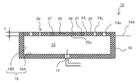
この面照明光源装置10は、発光ダイオード等の光を放射する単体又は複数の集合体からなる一群の光源12と、この光源12からの光を伝搬してその放射方向の所定位置に放射面14Aを有する光学的に透明な導光体14と、この導光体14の放射面14A以外の面を閉鎖し、光源12を略中央に配置した無蓋のケーシング16と、を備えている。
The surface illumination
本実施形態では、ケーシング16の大きさとして、例えば10cm×10cm×1.5cm(高さ)の直方体を採用している。但し、このケーシング16の大きさは、これに限定されるものではない。また、ケーシング16の材質も、特に限定されるものではないが、例えば金属や合成樹脂が用いられる。
In the present embodiment, as the size of the
導光体14は、例えば、光学ガラスにより構成することができるし、アクリル樹脂等の透明度の良いプラスチックを使用することができる。また、シリコン樹脂等の柔軟な透明プラスチックを用いてもよい。さらに、気体や液体であっても良い。なお、本実施形態では、導光体3が空気である場合を例として説明する。
The
ケーシング16と導光体14との間の全体には、内側反射手段としての底面反射部18A及び側面反射部18Bを有する内側反射部18が設けられている。また、放射面14A上には、放射側反射手段としての放射側反射部20が設けられている。
An entire inner portion between the
これら内側反射部18及び放射側反射部20には、いずれも光吸収の少ない材質が用いられている。そして、内側反射部18及び放射側反射部20は、超微細発泡光反射板、チタンホワイトの微粒子をエマルジョン化したもの、ポリテトラフロロエチレン(poly
fluoro carbon)の微粒子のいずれか、またはこれらの組み合わせたものからなっている。
The
Fluoro carbon) or a combination thereof.
放射側反射部20は、放射面14A上に配置され導光体14の内部を伝搬する光を所定
の割合で反射させる反射面22aを有する外方反射部22と、この外方反射部22に形成され光源12からの光のうち少なくとも1回はいずれかの反射面(反射面22aや内側反射部18等)で反射された反射光を通過させる開口部24と、を有している。
The radiation-
外方反射部22は、光の放射方向の厚さt(図1B参照)が略均一に形成されている。この外方反射部22には、光源12に対向する放射面14Aの中心側に、同心状に多数の未貫通孔(ハーフカット孔)26と、その外周側に幅狭の多数の幅狭溝27が形成されている。この幅狭溝27は、放射面14Aの中心に対し同心状かつ不連続な環状(方形リング状)に形成されている。すなわち、幅狭溝27は、未貫通(ハーフカット)の接続部23により不連続な方形リング状に形成されている。不連続な方形リング状でないとすると、放射側反射部20から外方反射部22の中心側のみが離脱してしまうからである。
The
なお、これら未貫通孔26及び幅狭溝27は、光源12からの光の反射量(又は光の透過量)を調節するために設けられるものである。
開口部24は、光源12に対向する放射面14Aの中心に対し、放射面14Aに沿って中心軸対称に形成された多数の丸孔(貫通孔)241、242、・・・24nを有している。これらの丸孔24には、光を反射する側面壁24aが形成されている。光源12から放射された光は、少なくとも1回は、内側反射部18の底面反射部18A、側面反射部18B、外方反射部22の反射面22a、又は側面壁24aにおいて反射されて開口部24を通過する。すなわち、光源12から放射された光が直接的に開口部24を通過することがないように構成されている。
The
The
開口部24の丸孔241、242、・・・24nは、その孔径が均一ではなく、光源12に対向する放射面14Aの中心から放射面14Aに沿って遠ざかるに従い、その径が変化するように設定されている。その変化の程度については、図3で後述する。
24 n of the round holes 24 1 , 24 2 ,... 24 n of the
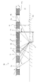
図2は、放射側反射部20の拡大断面図を示している。
外方反射部22の中心側の未貫通孔26は、例えば断面V字状又は断面矩形状の凹部に形成されている。この未貫通孔26によって、外方反射部22の反射量(すなわち、外方反射部22の内部を透過する光の透過量)を調整している。この外方反射部22は、光源12との対向面側に光を所定の割合で反射させる反射面22aを有するが、光が内部をわずかに透過する性質も有している。このため、未貫通孔26が形成された部分の外方反射部22の厚みを変化させることで、光の透過量を調整している。
FIG. 2 shows an enlarged cross-sectional view of the radiation-
The
この未貫通孔26は、光源12に対向する放射面14Aの中心Oの近傍に複数個が形成されている。この未貫通孔26は、放射面14Aの中心位置Oから放射面14Aに沿って外方に遠ざかるに従い、その孔寸法及び深さが大きくなるように形成されている。これは、光源12の指向性等に起因して、中心位置Oから外方に遠ざかるに従い光量が減少するため、それに応じて未貫通孔26での透過光量が多くなるように調節するためである。
A plurality of the
なお、本実施形態では、未貫通孔26を、放射側反射部20の外側面(反射面22aと反対側)に形成した場合について説明したが、これに限らず、放射側反射部20の内側面(反射面22aと同じ側)に形成してもよい。
In the present embodiment, the case where the
さらに、複数形成された未貫通孔26の外周側には、放射面14Aの中心Oを中心軸対称として幅狭の幅狭溝27が複数形成されている。この幅狭溝27も、外方反射部22の内部を透過する光の透過量を調整する役目をなす。なお、これら未貫通孔26と幅狭溝27とは、いずれも光の反射量(透過量)を調整するものではあるが、幅狭溝27は未貫通孔26よりも光の反射量(透過量)をより多くの割合で調整することができる。
Further, a plurality of
また、開口部24は、光源12から放射された光が直接的に該開口部24を通過しないような位置及び大きさに形成されている。これは、光源12から放射された光が開口部24を直接的に通過すると、放射側反射部20を通過した光の光束が強すぎることになるためである。この場合は、放射面14Aから光の放射方向に所定距離離間した位置での光の分布を均一にするのは困難となる。
The
よって、本実施形態では、光源12からの光のうち少なくとも1回はいずれかの反射面で反射された反射光のみを開口部24にて通過させるようにしている。このために、開口部24の位置及び大きさは、次の条件を満足するように放射側反射部20に形成されている。
Therefore, in the present embodiment, only the reflected light reflected by any one of the reflecting surfaces is allowed to pass through the
すなわち、光源12に対向する放射面14Aの中心Oから放射面14Aに沿って開口部24までの最小距離をx、光源12から外方反射部22までの放射方向の離間距離をd、開口部24の直径をa、外方反射部22の厚さをtとしたとき、
d/x<t/a
の関係を有する。
That is, the minimum distance from the center O of the radiating
d / x <t / a
Have the relationship.
これにより、光源12から放射された光が直接的に開口部24を通過するのが防止される。また、光源12から放射された光は、少なくとも1回は内側反射部18の反射面又は外方反射部22の反射面22a、あるいは開口部24の側面壁24aにて反射した反射光のみを通過させることになる。このため、放射側反射部20を通過した光(反射光)により、放射面14Aから所定距離離れた位置での光の分布が均一になる。
Thereby, the light emitted from the
更に、この開口部24も、放射面14Aの中心位置Oから外方に遠ざかるに従い、その孔径が大きくなるように形成されている。
すなわち、予め設定した基準面積に対する開口部24の面積和の比率を開口率A(所定部分の開口部24の面積/基準面積)とし、
b、cを定数、
x(mm)を光源12に対向する放射面14Aの中心Oからの距離としたとき、概略
A=bx2+c
の関係を有する。
Further, the
That is, the ratio of the area sum of the
b and c are constants,
When x (mm) is a distance from the center O of the
Have the relationship.
これは、図3に示すように、横軸に距離xをとり縦軸に開口率Aをとると、いわゆる2次曲線となる。なお、開口率A=1は全開の状態を意味する。
この図3で、本実施形態では、b=0.000375とし、また、定数cは、例えば光源12に対向する放射面14Aの中心Oに未貫通孔26があればc=0.04に設定しておく。これにより、x=0の点の開口率A=0.04となる。
As shown in FIG. 3, this is a so-called quadratic curve when the distance x is on the horizontal axis and the aperture ratio A is on the vertical axis. The aperture ratio A = 1 means a fully open state.
In FIG. 3, in this embodiment, b = 0.000375, and the constant c is set to c = 0.04 if there is a
この図3に示すように、開口率Aは、光源12に対向する放射面14Aの中心Oから放射面14Aに沿って外方に遠ざかるに従い距離の2乗に比例して大きくなっている。具体的には、図1Aで示すように、放射面14Aの中心Oから外方に遠ざかるに従い、開口部24の大きさ(径)が大となるように設計している。
As shown in FIG. 3, the aperture ratio A increases in proportion to the square of the distance from the center O of the
本実施形態によれば、開口部24では、光源12からの光のうち少なくとも1回はいずれかの反射面で反射された反射光を通過させるようにしたので、放射側反射部20の表面から光の放射方向に所定の距離(例えば5mm)以上離れた面において均一な照明光を得ることができた。
According to the present embodiment, the
また、本実施形態では、外方反射部22での光の反射量を調節する未貫通孔26と幅狭溝27を設けたので、光源12からの光を微妙にコントロールして均一な照明光を得るこ
とができる。
In the present embodiment, the
さらに、開口率Aを数式で定義することで、開口部24の寸法を定量的に設定することができる。このため、開口部24の加工作業が容易となる。
(第2の実施の形態)
図4は、第2の実施の形態の面照明光源装置の構成を示す図である。
Furthermore, the dimension of the
(Second Embodiment)
FIG. 4 is a diagram illustrating a configuration of the surface illumination light source device according to the second embodiment.
なお、本実施形態では、図1Bに示した光源12、導光体14、及びケーシング16の図示を省略し、放射側反射部30のみを図示している。
本実施形態の放射側反射部30は、放射面14A上に配置され導光体14の内部を伝搬する光を所定の割合で反射させる反射面32aを有する外方反射部32と、この外方反射部32に形成され光源12からの光のうち少なくとも1回はいずれかの反射面(反射面32aや内側反射部18等)で反射された反射光を通過させる開口部34と、を有している。
In the present embodiment, illustration of the
The radiation-
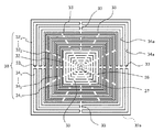
外方反射部32は、光の放射方向の厚さt(図1B参照)が略均一に形成されている。この外方反射部32には、光源12に対向する放射面14Aの中心側に、同心状に多数の未貫通孔(ハーフカット孔)36と、その外周側に幅狭の多数の幅狭溝37が形成されている。この幅狭溝37は、放射面14Aの中心に対し同心状かつ不連続な環状(方形リング状)に形成されている。すなわち、幅狭溝37は、接続部33により不連続な方形リング状に形成されている。不連続な方形リング状でないとすると、放射側反射部30から外方反射部32の中心側のみが離脱してしまうからである。
The
なお、これら未貫通孔36及び幅狭溝37は、前述したように、光源12からの光の反射量(又は光の透過量)を調節するために設けられるものである。すなわち、不均一な照明が生じるのを防止し、均一な照明を得ることができるようにしている。
The
また、開口部34は、光源12に対向する放射面14Aの中心から放射面14Aに沿って外方に、所定の間隔を隔てて中心軸対称に方形リング状の環状孔341、342、・・・34nが形成されている。この環状孔34は、その幅寸法が均一ではなく、光源12に対向する放射面14Aの中心から放射面14Aに沿って遠ざかるに従い、その寸法が変化している。その変化の程度については、図3で説明した通りである。この環状孔34には、光を反射する側面壁34aが形成されている。
In addition, the
光源12から放射された光は、少なくとも1回は、図1Bに示した内側反射部18の底面反射部18A、側面反射部18B、外方反射部32の反射面32a、又は側面壁34aにおいて反射されて開口部34を通過する。すなわち、光源12から放射された光が直接的に開口部34を通過することがないように構成されている。
The light emitted from the
また、外方反射部32には、隣接する環状孔34n,34n−1の間を接続する接続部33が形成されている。この接続部33は、放射面14Aの中心から放射状に延びている。本実施形態では、方形リング状の環状孔34が中心軸対称に形成されているので、これらを接続するものがないと外方反射部32がばらばらに離脱してしまう。これを防止するため、接続部33によりこれらを一体的に接続している。
Further, the
なお、この接続部33は、その位置、大きさ、方向を任意に設定したのでは、均一な照明光を得ることが困難となる。そこで、接続部33の位置、大きさ、方向は実験によって最適な条件から求めている。
(第3の実施の形態)
図5は、第3の実施の形態の面照明光源装置の構成を示す図である。
Note that it is difficult to obtain uniform illumination light if the position, size, and direction of the connecting
(Third embodiment)
FIG. 5 is a diagram illustrating a configuration of the surface illumination light source device according to the third embodiment.
なお、本実施形態では、図1Bに示した光源12、導光体14、及びケーシング16の図示を省略し、放射側反射部40のみを図示している。
本実施形態の放射側反射部40は、放射面14A上に配置され導光体14の内部を伝搬する光を所定の割合で反射させる反射面42aを有する外方反射部42と、この外方反射部42に形成され光源12からの光のうち少なくとも1回はいずれかの反射面(反射面42aや内側反射部18等)で反射された反射光を通過させる開口部44と、を有している。
In the present embodiment, illustration of the
The radiation-
外方反射部42は、光の放射方向の厚さt(図1B参照)が略均一に形成されている。この外方反射部42には、光源12に対向する放射面14Aの中心側に、同心状かつ不連続な幅狭の多数の円形リング状の幅狭溝47が形成されている。すなわち、円形リング状の幅狭溝47は、接続部43により不連続な環状に形成されている。不連続な環状としたのは、若しも連続な環状に形成したとすると、放射側反射部40から外方反射部42の中心側のみが離脱してしまうからである。
The
なお、この幅狭溝47は、光源12からの光の反射量(又は光の透過量)を調節するために設けられるものである。また、この外方反射部42の中心側に、必要に応じて未貫通孔(ハーフカット孔)を設けてもよい。
The
開口部44は、光源12に対向する放射面14Aの中心に対し中心軸対称に形成された多数の丸孔(貫通孔)441、442、・・・44nを有している。これらの丸孔44には、光を反射する側面壁44aが形成されている。光源12から放射された光は、少なくとも1回は、図1Bに示した内側反射部18の底面反射部18A、側面反射部18B、外方反射部42の反射面42a、又は側面壁44aにおいて反射されて開口部44を通過する。すなわち、光源12から放射された光が直接的に開口部44を通過することがないように構成されている。
The
開口部24の各丸孔441、442、・・・44nは、その孔径が均一ではなく、光源12に対向する放射面14Aの中心から放射面14Aに沿って遠ざかるに従い、その径が変化するように設定されている。その変化の程度については、図3で説明した通りである。
Each of the round holes 44 1 , 44 2 ,... 44 n of the
なお、以上説明した各実施形態では、開口部24、34,44の形状として丸孔や方形リング状の連続的又は不連続な環状孔として説明したが、これらに限らない。例えば、開口部24、34,44が角孔であってもよいし、円形リング状の環状孔であってもよい。(第4の実施の形態)
図6は、面照明光源装置10を複数配置して構成された面照明装置10’の実施形態を示す図である。なお、図1と同一又は相当する部材には同一の符号を付している。
In each of the embodiments described above, the
FIG. 6 is a diagram showing an embodiment of a
なお、この面照明装置10’は、内容把握を容易にするため放射側反射部20の図示を省略している。実際には、面照明光源装置10の夫々について、放射側反射部20が形成されている。
In the
本実施形態によれば、個々の面照明光源装置10の放射面14Aから光の放射方向に所定の距離離れた面において得られる均一な照明光の領域を任意に拡大することができる。このため、複数の面照明光源装置10をマトリクス状に配置すれば、必要な領域範囲において均一な照明光を得ることができる。
According to the present embodiment, it is possible to arbitrarily enlarge the area of uniform illumination light obtained on a surface separated from the
10 面照明光源装置
10’ 面照明装置
12 光源
14 導光体
14A 放射面
16 ケーシング
18 内側反射部
18A 底面反射部
18B 側面反射部
20 放射側反射部
22 外方反射部
22a 反射面
23 接続部
24 開口部
241・・・24n 丸孔
24a 側面壁
26 未貫通孔
27 幅狭溝
30 放射側反射部
32 外方反射部
32a 反射面
33 接続部
34 開口部
341・・・34n 環状孔
34a 側面壁
36 未貫通孔
37 幅狭溝
40 放射側反射部
42 外方反射部
42a 反射面
43 接続部
44 開口部
441・・・44n 丸孔
44a 側面壁
47 幅狭溝
DESCRIPTION OF
Claims (15)
該光源からの光を伝搬してその放射方向の所定位置に放射面を有する光学的に透明な導光体と、
該導光体の前記放射面以外の面を閉鎖し、光を反射させる底面及び側面反射部からなる内側反射手段が設けられ、その底面の中央部に前記光源が配設されたケーシングと、
前記放射面状に配置された放射側反射手段とを備え、
前記放射側反射手段は前記導光体内部を伝搬する光を所定の割合で透過及び反射させる部材からなり、該放射側反射手段の周辺部に開口部を設けると共に、中心部を未開口部としておくことによって、前記放射側反射手段の透過光量が前記光源に対向する前記放射面の中心位置から外方に遠ざかるに従い多くなるように調節されていることを特徴とする面照明光源装置。 A group of light sources consisting of a single point light source that emits light or a collection of a plurality of point light sources;
An optically transparent light guide that propagates light from the light source and has a radiation surface at a predetermined position in the radiation direction;
A casing in which a surface other than the radiation surface of the light guide is closed, and an inner reflection means including a bottom surface and a side surface reflection portion for reflecting light is provided, and the light source is disposed in a central portion of the bottom surface ;
Radiation side reflecting means arranged in the radiation surface,
The radiation-side reflecting means is made of a member that transmits and reflects light propagating through the light guide at a predetermined ratio. An opening is provided in the periphery of the radiation-side reflecting means, and the center is not opened. The surface illumination light source device is characterized in that the amount of transmitted light of the radiation side reflecting means is adjusted to increase as it moves away from the center position of the radiation surface facing the light source.
A=bxA = bx 22 +c (1)式+ C (1) Formula
を満たすことを特徴とする請求項1に記載の面照明光源装置。The surface illumination light source device according to claim 1, wherein:
d/x<t/a
の関係を有することを特徴とする請求項1に記載の面照明光源装置。 The distance from the center of the radiation surface facing the light source to the opening along the radiation surface is x, the distance in the radiation direction from the light source to the radiation-side reflecting means is d, and the opening of the opening. When the dimension is a and the thickness of the radiation side reflection means is t,
d / x <t / a
The surface illumination light source device according to claim 1, wherein:
Priority Applications (7)
| Application Number | Priority Date | Filing Date | Title |
|---|---|---|---|
| JP2007164796A JP4764962B2 (en) | 2007-06-22 | 2007-06-22 | Surface illumination light source device and surface illumination device |
| CN2008800213316A CN101743431B (en) | 2007-06-22 | 2008-06-20 | Surface illuminating light source device and surface illuminating device |
| KR1020097026100A KR101086523B1 (en) | 2007-06-22 | 2008-06-20 | Surface illuminating light source device |
| TW97123084A TWI420053B (en) | 2007-06-22 | 2008-06-20 | Surface lighting device and surface lighting device |
| EP08764180.9A EP2163807B1 (en) | 2007-06-22 | 2008-06-20 | Surface illuminating light source device and surface illuminating device |
| PCT/JP2008/001597 WO2009001532A1 (en) | 2007-06-22 | 2008-06-20 | Surface illuminating light source device and surface illuminating device |
| US12/665,673 US8272772B2 (en) | 2007-06-22 | 2008-06-20 | Surface illuminating light source device and surface illuminating device |
Applications Claiming Priority (1)
| Application Number | Priority Date | Filing Date | Title |
|---|---|---|---|
| JP2007164796A JP4764962B2 (en) | 2007-06-22 | 2007-06-22 | Surface illumination light source device and surface illumination device |
Publications (3)
| Publication Number | Publication Date |
|---|---|
| JP2009004248A JP2009004248A (en) | 2009-01-08 |
| JP2009004248A5 JP2009004248A5 (en) | 2010-05-27 |
| JP4764962B2 true JP4764962B2 (en) | 2011-09-07 |
Family
ID=40185359
Family Applications (1)
| Application Number | Title | Priority Date | Filing Date |
|---|---|---|---|
| JP2007164796A Expired - Fee Related JP4764962B2 (en) | 2007-06-22 | 2007-06-22 | Surface illumination light source device and surface illumination device |
Country Status (7)
| Country | Link |
|---|---|
| US (1) | US8272772B2 (en) |
| EP (1) | EP2163807B1 (en) |
| JP (1) | JP4764962B2 (en) |
| KR (1) | KR101086523B1 (en) |
| CN (1) | CN101743431B (en) |
| TW (1) | TWI420053B (en) |
| WO (1) | WO2009001532A1 (en) |
Cited By (1)
| Publication number | Priority date | Publication date | Assignee | Title |
|---|---|---|---|---|
| US9081229B2 (en) | 2009-11-16 | 2015-07-14 | Opto Design, Inc. | Surface light source unit, surface illumination device, and liquid crystal display device |
Families Citing this family (32)
| Publication number | Priority date | Publication date | Assignee | Title |
|---|---|---|---|---|
| JP2010205515A (en) * | 2009-03-02 | 2010-09-16 | Opt Design:Kk | Plane lighting unit, and plane lighting system using this plane lighting unit |
| JP5531209B2 (en) * | 2009-03-02 | 2014-06-25 | 株式会社オプトデザイン | LED substrate, LED lighting unit and LED lighting device |
| JP5515001B2 (en) * | 2009-09-02 | 2014-06-11 | 株式会社オプトデザイン | Surface illumination light source device and surface illumination device using the surface illumination light source device |
| JP5540610B2 (en) * | 2009-09-03 | 2014-07-02 | 株式会社Jvcケンウッド | Light quantity control member, surface light source device and display device |
| CN102483199B (en) * | 2009-09-11 | 2015-01-21 | Opto设计股份有限公司 | Surface illumination method using point light source, linear light source device, and surface illumination device using linear light source device |
| JP5320599B2 (en) * | 2009-09-18 | 2013-10-23 | 株式会社オプトデザイン | Light source device and surface illumination device using the light source device |
| JP5515002B2 (en) * | 2009-09-18 | 2014-06-11 | 株式会社オプトデザイン | Surface illumination light source device and surface illumination device using the surface illumination light source device |
| WO2011132787A1 (en) * | 2010-04-23 | 2011-10-27 | 株式会社オプトデザイン | Surface illumination fixture and surface illumination device |
| WO2011162258A1 (en) | 2010-06-25 | 2011-12-29 | 株式会社オプトデザイン | Illumination device |
| JP5515005B2 (en) * | 2010-07-16 | 2014-06-11 | 株式会社オプトデザイン | Lighting device |
| JP5584852B2 (en) * | 2010-07-16 | 2014-09-10 | 株式会社オプトデザイン | Surface illumination light source device |
| CN102644883A (en) * | 2011-03-25 | 2012-08-22 | 京东方科技集团股份有限公司 | Direct type backlight source |
| JP5606395B2 (en) * | 2011-05-30 | 2014-10-15 | 三菱電機株式会社 | In-vehicle information equipment |
| JP5842274B2 (en) | 2011-06-09 | 2016-01-13 | 株式会社オプトデザイン | Lighting device |
| DE102012205188A1 (en) | 2012-03-30 | 2013-10-02 | Tridonic Gmbh & Co. Kg | LED lamp has perforated plate that is provided with several holes which are filled with transparent material, and light exit opening is provided at front of housing, through which primary light of main light beam of LED is made to pass |
| CN202629814U (en) * | 2012-05-31 | 2012-12-26 | 京东方科技集团股份有限公司 | Lateral backlight module |
| WO2014013745A1 (en) * | 2012-07-20 | 2014-01-23 | Sharp Kabushiki Kaisha | Lighting device and method for providing light |
| TWI510841B (en) * | 2013-07-23 | 2015-12-01 | Au Optronics Corp | Display device |
| CN105518380B (en) * | 2013-09-06 | 2019-01-29 | 传感器电子技术股份有限公司 | Ultraviolet light diffusion irradiation |
| JP6315179B2 (en) * | 2014-03-17 | 2018-04-25 | Tianma Japan株式会社 | Surface light emitting device and liquid crystal display device |
| WO2015146959A1 (en) | 2014-03-27 | 2015-10-01 | 東レ株式会社 | Reflecting sheet, reflection unit for surface light source device, and surface light source device |
| CN104165329B (en) * | 2014-08-13 | 2016-08-17 | 福建省锐驰电子科技有限公司 | One can plastic uptake reflector plate |
| TWI547741B (en) * | 2014-12-05 | 2016-09-01 | 友達光電股份有限公司 | Thin type backlight module |
| KR20180005786A (en) * | 2016-07-06 | 2018-01-17 | 삼성디스플레이 주식회사 | Backlight unit, display device including the same, and fabrication method thereof |
| US10809571B2 (en) | 2017-01-31 | 2020-10-20 | Sharp Kabushiki Kaisha | Lighting device and display device |
| CN109946873A (en) * | 2017-12-20 | 2019-06-28 | 鸿富锦精密工业(深圳)有限公司 | Backlight module |
| CN111208670A (en) * | 2018-11-22 | 2020-05-29 | 瑞仪(广州)光电子器件有限公司 | Light-emitting mechanism, backlight module and display device thereof |
| US11880057B2 (en) | 2019-06-26 | 2024-01-23 | Corning Incorporated | Display device and backlight unit therefor |
| WO2021162889A1 (en) | 2020-02-10 | 2021-08-19 | Corning Incorporated | Backlights including patterned reflectors |
| US11835213B2 (en) * | 2021-08-19 | 2023-12-05 | Matthew Hartley | Lighting fixtures with improved lighting components |
| DE102022113516A1 (en) | 2022-05-30 | 2023-11-30 | Lisa Dräxlmaier GmbH | LIGHTING DEVICE FOR A VEHICLE INTERIOR PART WITH HOMOGENEOUS LIGHT DISTRIBUTION |
| CN115220261A (en) * | 2022-06-09 | 2022-10-21 | 武汉华星光电技术有限公司 | Backlight module and display module |
Family Cites Families (16)
| Publication number | Priority date | Publication date | Assignee | Title |
|---|---|---|---|---|
| JPH02183903A (en) * | 1989-01-10 | 1990-07-18 | Fujitsu Ltd | Face luminescence device |
| JPH08153405A (en) * | 1994-06-21 | 1996-06-11 | Nakaya:Kk | Planar light source |
| JPH10233112A (en) * | 1997-02-18 | 1998-09-02 | Tootasu Japan:Kk | Surface light source device and its manufacture |
| JP2002343124A (en) | 2001-05-15 | 2002-11-29 | Mitsubishi Rayon Co Ltd | Surface light source equipment |
| JP2003186427A (en) | 2001-12-20 | 2003-07-04 | Yazaki Corp | Lighting type display device |
| TWI258624B (en) * | 2004-03-11 | 2006-07-21 | Samsung Corning Co Ltd | Surface light source device and back light unit having the same |
| TWI247176B (en) | 2004-03-30 | 2006-01-11 | Chi Mei Optoelectronics Corp | Direct point light source backlight module and liquid crystal display using the same |
| JP4397728B2 (en) | 2004-04-21 | 2010-01-13 | 日東電工株式会社 | Direct type backlight |
| KR20050121076A (en) | 2004-06-21 | 2005-12-26 | 삼성전자주식회사 | Back light assembly and display device having the same |
| KR101085444B1 (en) | 2004-06-25 | 2011-11-21 | 삼성전자주식회사 | Optical member and back light assembly having the light guide plate, and display device having the back light assembly |
| EP1623630A1 (en) | 2004-08-03 | 2006-02-08 | Pancosma S.A. | Powdered sweetener for human nutrition |
| JP3875247B2 (en) * | 2004-09-27 | 2007-01-31 | 株式会社エンプラス | Light emitting device, surface light source device, display device, and light flux controlling member |
| CN100420050C (en) * | 2004-10-19 | 2008-09-17 | 欧姆龙株式会社 | A light emitting source and a light emitting source array |
| TWM274547U (en) * | 2005-04-22 | 2005-09-01 | San Ho Entpr Co Ltd | Back-light module |
| TWM284012U (en) * | 2005-07-20 | 2005-12-21 | Wen-Gung Sung | Backlight module structure for LEDs arranged on a big surface |
| JP4631628B2 (en) * | 2005-09-13 | 2011-02-16 | 日本電気株式会社 | Lighting device and display device |
-
2007
- 2007-06-22 JP JP2007164796A patent/JP4764962B2/en not_active Expired - Fee Related
-
2008
- 2008-06-20 WO PCT/JP2008/001597 patent/WO2009001532A1/en active Application Filing
- 2008-06-20 US US12/665,673 patent/US8272772B2/en active Active
- 2008-06-20 EP EP08764180.9A patent/EP2163807B1/en not_active Not-in-force
- 2008-06-20 TW TW97123084A patent/TWI420053B/en not_active IP Right Cessation
- 2008-06-20 CN CN2008800213316A patent/CN101743431B/en not_active Expired - Fee Related
- 2008-06-20 KR KR1020097026100A patent/KR101086523B1/en active IP Right Grant
Cited By (1)
| Publication number | Priority date | Publication date | Assignee | Title |
|---|---|---|---|---|
| US9081229B2 (en) | 2009-11-16 | 2015-07-14 | Opto Design, Inc. | Surface light source unit, surface illumination device, and liquid crystal display device |
Also Published As
| Publication number | Publication date |
|---|---|
| KR20100009585A (en) | 2010-01-27 |
| JP2009004248A (en) | 2009-01-08 |
| EP2163807A1 (en) | 2010-03-17 |
| KR101086523B1 (en) | 2011-11-23 |
| EP2163807A4 (en) | 2010-12-08 |
| WO2009001532A1 (en) | 2008-12-31 |
| CN101743431A (en) | 2010-06-16 |
| US8272772B2 (en) | 2012-09-25 |
| TW200914770A (en) | 2009-04-01 |
| TWI420053B (en) | 2013-12-21 |
| EP2163807B1 (en) | 2016-07-06 |
| US20100177535A1 (en) | 2010-07-15 |
| CN101743431B (en) | 2012-09-05 |
Similar Documents
| Publication | Publication Date | Title |
|---|---|---|
| JP4764962B2 (en) | Surface illumination light source device and surface illumination device | |
| US9268082B2 (en) | Free form lighting module | |
| JP6315179B2 (en) | Surface light emitting device and liquid crystal display device | |
| US9291767B2 (en) | Free form lighting module | |
| US8408752B2 (en) | Surface lighting unit, surface lighting light source device, surface lighting device | |
| JP6188641B2 (en) | Surface light source device and display device | |
| JP4491540B2 (en) | Optical reflector, surface illumination light source device, and surface illumination device | |
| KR20130082084A (en) | Planar light source device and illumination apparatus | |
| JP5119379B2 (en) | Surface illumination light source device and surface illumination device | |
| JP2011065973A (en) | Surface illumination light source device, and surface illumination device using this surface illumination light source device | |
| JP3211553U (en) | Lighting device | |
| EP3440401B1 (en) | A lens with slits | |
| KR200478823Y1 (en) | Lighting unit using optical sheet | |
| KR20120103503A (en) | Surface light source unit, surface illumination light source device, and surface illumination device | |
| KR101427512B1 (en) | Direct-lighting light source including supporting plate for preventing bending of reflection member having light passage | |
| EP2573458A1 (en) | Lighting device with uniformized luminous intensity | |
| TWM460414U (en) | High light uniformity LED module | |
| JP2014096348A (en) | Lighting device | |
| JP2012204215A (en) | Lighting system and lighting equipment equipped with the same |
Legal Events
| Date | Code | Title | Description |
|---|---|---|---|
| RD01 | Notification of change of attorney |
Free format text: JAPANESE INTERMEDIATE CODE: A7421 Effective date: 20090223 |
|
| A521 | Request for written amendment filed |
Free format text: JAPANESE INTERMEDIATE CODE: A523 Effective date: 20090313 |
|
| A521 | Request for written amendment filed |
Free format text: JAPANESE INTERMEDIATE CODE: A523 Effective date: 20100412 |
|
| A621 | Written request for application examination |
Free format text: JAPANESE INTERMEDIATE CODE: A621 Effective date: 20100412 |
|
| A871 | Explanation of circumstances concerning accelerated examination |
Free format text: JAPANESE INTERMEDIATE CODE: A871 Effective date: 20100412 |
|
| TRDD | Decision of grant or rejection written | ||
| A975 | Report on accelerated examination |
Free format text: JAPANESE INTERMEDIATE CODE: A971005 Effective date: 20100930 |
|
| A01 | Written decision to grant a patent or to grant a registration (utility model) |
Free format text: JAPANESE INTERMEDIATE CODE: A01 Effective date: 20101005 |
|
| A61 | First payment of annual fees (during grant procedure) |
Free format text: JAPANESE INTERMEDIATE CODE: A61 Effective date: 20101019 |
|
| R150 | Certificate of patent or registration of utility model |
Ref document number: 4764962 Country of ref document: JP Free format text: JAPANESE INTERMEDIATE CODE: R150 Free format text: JAPANESE INTERMEDIATE CODE: R150 |
|
| FPAY | Renewal fee payment (event date is renewal date of database) |
Free format text: PAYMENT UNTIL: 20140624 Year of fee payment: 3 |
|
| R250 | Receipt of annual fees |
Free format text: JAPANESE INTERMEDIATE CODE: R250 |
|
| R250 | Receipt of annual fees |
Free format text: JAPANESE INTERMEDIATE CODE: R250 |
|
| R250 | Receipt of annual fees |
Free format text: JAPANESE INTERMEDIATE CODE: R250 |
|
| R250 | Receipt of annual fees |
Free format text: JAPANESE INTERMEDIATE CODE: R250 |
|
| R250 | Receipt of annual fees |
Free format text: JAPANESE INTERMEDIATE CODE: R250 |
|
| R250 | Receipt of annual fees |
Free format text: JAPANESE INTERMEDIATE CODE: R250 |
|
| R250 | Receipt of annual fees |
Free format text: JAPANESE INTERMEDIATE CODE: R250 |
|
| S531 | Written request for registration of change of domicile |
Free format text: JAPANESE INTERMEDIATE CODE: R313531 |
|
| R350 | Written notification of registration of transfer |
Free format text: JAPANESE INTERMEDIATE CODE: R350 |
|
| R250 | Receipt of annual fees |
Free format text: JAPANESE INTERMEDIATE CODE: R250 |
|
| R250 | Receipt of annual fees |
Free format text: JAPANESE INTERMEDIATE CODE: R250 |
|
| S111 | Request for change of ownership or part of ownership |
Free format text: JAPANESE INTERMEDIATE CODE: R313113 |
|
| R350 | Written notification of registration of transfer |
Free format text: JAPANESE INTERMEDIATE CODE: R350 |
|
| LAPS | Cancellation because of no payment of annual fees |