JP4762002B2 - Electronics - Google Patents
Electronics Download PDFInfo
- Publication number
- JP4762002B2 JP4762002B2 JP2006050600A JP2006050600A JP4762002B2 JP 4762002 B2 JP4762002 B2 JP 4762002B2 JP 2006050600 A JP2006050600 A JP 2006050600A JP 2006050600 A JP2006050600 A JP 2006050600A JP 4762002 B2 JP4762002 B2 JP 4762002B2
- Authority
- JP
- Japan
- Prior art keywords
- housing
- protrusions
- protrusion
- cable
- harness
- Prior art date
- Legal status (The legal status is an assumption and is not a legal conclusion. Google has not performed a legal analysis and makes no representation as to the accuracy of the status listed.)
- Expired - Fee Related
Links
Images


Classifications
-
- H—ELECTRICITY
- H01—ELECTRIC ELEMENTS
- H01R—ELECTRICALLY-CONDUCTIVE CONNECTIONS; STRUCTURAL ASSOCIATIONS OF A PLURALITY OF MUTUALLY-INSULATED ELECTRICAL CONNECTING ELEMENTS; COUPLING DEVICES; CURRENT COLLECTORS
- H01R13/00—Details of coupling devices of the kinds covered by groups H01R12/70 or H01R24/00 - H01R33/00
- H01R13/58—Means for relieving strain on wire connection, e.g. cord grip, for avoiding loosening of connections between wires and terminals within a coupling device terminating a cable
- H01R13/5833—Means for relieving strain on wire connection, e.g. cord grip, for avoiding loosening of connections between wires and terminals within a coupling device terminating a cable the cable being forced in a tortuous or curved path, e.g. knots in cable
-
- H—ELECTRICITY
- H01—ELECTRIC ELEMENTS
- H01R—ELECTRICALLY-CONDUCTIVE CONNECTIONS; STRUCTURAL ASSOCIATIONS OF A PLURALITY OF MUTUALLY-INSULATED ELECTRICAL CONNECTING ELEMENTS; COUPLING DEVICES; CURRENT COLLECTORS
- H01R13/00—Details of coupling devices of the kinds covered by groups H01R12/70 or H01R24/00 - H01R33/00
- H01R13/648—Protective earth or shield arrangements on coupling devices, e.g. anti-static shielding
- H01R13/658—High frequency shielding arrangements, e.g. against EMI [Electro-Magnetic Interference] or EMP [Electro-Magnetic Pulse]
- H01R13/6591—Specific features or arrangements of connection of shield to conductive members
- H01R13/65912—Specific features or arrangements of connection of shield to conductive members for shielded multiconductor cable
-
- H—ELECTRICITY
- H01—ELECTRIC ELEMENTS
- H01R—ELECTRICALLY-CONDUCTIVE CONNECTIONS; STRUCTURAL ASSOCIATIONS OF A PLURALITY OF MUTUALLY-INSULATED ELECTRICAL CONNECTING ELEMENTS; COUPLING DEVICES; CURRENT COLLECTORS
- H01R4/00—Electrically-conductive connections between two or more conductive members in direct contact, i.e. touching one another; Means for effecting or maintaining such contact; Electrically-conductive connections having two or more spaced connecting locations for conductors and using contact members penetrating insulation
- H01R4/58—Electrically-conductive connections between two or more conductive members in direct contact, i.e. touching one another; Means for effecting or maintaining such contact; Electrically-conductive connections having two or more spaced connecting locations for conductors and using contact members penetrating insulation characterised by the form or material of the contacting members
- H01R4/64—Connections between or with conductive parts having primarily a non-electric function, e.g. frame, casing, rail
Landscapes
- Shielding Devices Or Components To Electric Or Magnetic Fields (AREA)
- Insertion, Bundling And Securing Of Wires For Electric Apparatuses (AREA)
Description
本発明は、ケーブルを有する電子機器に係り、特にケーブルの被膜をアースする構造に関する。 The present invention relates to an electronic apparatus having a cable, and more particularly to a structure for grounding a cable coating.
例えばポータブルコンピュータのような電子機器は、筐体内に搭載された各種モジュールを接続するケーブルを備える。電子機器が備えるケーブルには種々のものがあるが、なかには例えば電磁波の発生を抑制するために導電性の被膜を有するものがある。 For example, an electronic device such as a portable computer includes a cable for connecting various modules mounted in a housing. There are various types of cables included in electronic devices, and some include, for example, a conductive coating for suppressing the generation of electromagnetic waves.
一方、ハーネス固定部材を備えた電装品箱が提供されている(例えば、特許文献1参照)。特許文献1に記載の複数のハーネス固定部材は、電装品箱の側面板に突設されている。ハーネス固定部材は、千鳥状に配列され、ハーネスのケーブルを蛇行させた状態で挟持する。
例えばケーブルの被膜を筐体のグランド層にアースする場合、ケーブルが例えば板金などを用いてグランド層に押し付けられたり、ケーブル被膜にアース線が別に取り付けられ、このアース線がグランド層に接続されたりする。すなわち、ケーブルの被膜をアースする場合、筐体にアース用の別部材を新たに設ける必要がある。
例えば特許文献1に記載のハーネス固定部材を用いても、ケーブルの被膜をアースするためにはアース用の別部材が必要である。
For example, when the cable cover is grounded to the ground layer of the housing, the cable is pressed against the ground layer using, for example, sheet metal, or a ground wire is separately attached to the cable cover, and this ground wire is connected to the ground layer. To do. That is, when the cable coating is grounded, a separate grounding member needs to be provided in the housing.
For example, even if the harness fixing member described in
本発明の目的は、筐体に取り付けられる別部材を設けることなく、ケーブルの被膜をアースする構造を備えた電子機器を得ることにある。 The objective of this invention is obtaining the electronic device provided with the structure which earth | grounds the film of a cable, without providing the separate member attached to a housing | casing.
上記目的を達成するため、本発明の一つの形態に係る電子機器は、第1の筐体と、第2の筐体と、上記第1の筐体と上記第2の筐体とを回動可能に連結したヒンジ部と、上記第2の筐体に収容されたモジュールと、上記モジュールに電気的に接続され、上記ヒンジ部を通って上記第2の筐体と上記第1の筐体とに延びるとともに、導電性の被膜を有したケーブルと、上記第2の筐体内に設けられたグランド層と、上記ヒンジ部と連結された上記第2の筐体の端部に設けられ、上記第2の筐体の内壁から突出した複数の突起であって、少なくともそのうち1つの突起は側面に上記グランド層に電気的に接続されるとともに上記ケーブルの導電性の被膜に接した導体層を有し、該突起と他の突起との間に配線された上記ケーブルを挟持した複数の突起と、を具備した。
To achieve the above object, an electronic device according to one embodiment of the present invention, the rotary a first housing, a second housing, and the first housing and the second housing and coupled to the hinge portion, and the second module accommodated in the housing, electrically connected to the module, the second housing through the hinge portion and the and the first housing extends in a cable have a conductive coating, said a ground layer provided on the second housing, provided at an end of the which is connected with the hinge portion and the second housing, said first a plurality of projections projecting from the inner wall of the second casing, at least of which one projection have a conductor layer in contact with the conductive coating Rutotomoni the cable is electrically connected to the ground layer on the side surface and, a plurality of which sandwiches the cable wired between the projections and the other protrusions And the cause, equipped with a.
この構成によれば、突起の導体層を介してケーブルの被膜がアースされる。これにより筐体に取り付けられる別部材を設けることなく、ケーブルの被膜がアースされる。 According to this configuration, the cable coating is grounded via the conductor layer of the protrusion. Thereby, the coating of the cable is grounded without providing another member attached to the housing.
以下に本発明の実施の形態を、ポータブルコンピュータに適用した図面に基づいて説明する。
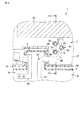
図1ないし図3は、本発明の第1の実施形態に係る電子機器としてのポータブルコンピュータ1を開示している。図1に示すように、ポータブルコンピュータ1は、本体2と、表示ユニット3と、本体2と表示ユニット3との間に設けられる一対のヒンジ部4,4とを備えている。
Hereinafter, embodiments of the present invention will be described with reference to the drawings applied to a portable computer.
1 to 3 disclose a
図1に示すように、本体2は、本体ベース6と本体カバー7とを備える。本体ベース6は、第1のハウジング部材の一例である。本体カバー7は、第2のハウジング部材の一例である。本体カバー7は、本体ベース6に上方から組み合わされる。これにより、本体2は、上壁8a、下壁8b、および側壁8cを有する箱状の筐体8を備える。筐体8は、回路基板9を収容している。回路基板9は、モジュールの一例である。
As shown in FIG. 1, the
筐体下壁8bの内壁8baには、第1のグランド層10が設けられている。第1のグランド層10は、例えば導電性の材料を塗布またはメッキするなどして形成されている。
A
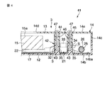
表示ユニット3は、ハウジングベース12とハウジングカバー13とを備える。ハウジングベース12は、第1のハウジング部材の一例である。ハウジングカバー13は、第2のハウジング部材の一例である。ハウジングカバー13は、ハウジングベース12に組み合わされる。これにより、表示ユニット3は、前壁14a、後壁14b、および側壁14cを有する箱状のディスプレイハウジング14を備える。
The
ディスプレイハウジング14は、液晶表示モジュール15を収容している。液晶表示モジュール15は、表示画面15aを有している。表示画面15aは、ディスプレイハウジング前壁14aの開口部14dを通じてディスプレイハウジング14の外部に露出している。
The
図1に示すように、ディスプレイハウジング後壁14bの内壁14baには、第2のグランド層17が設けられている。第2のグランド層17は、例えば導電性の材料を塗布またはメッキするなどして形成されている。ただし第1および第2のグランド層10,17は塗布またはメッキに限らず、例えば薄く引き延ばしたアルミニウムや銅のような金属箔を張り付けて形成しても良い。
As shown in FIG. 1, a
ヒンジ部4は、本体2の後端部に設けられ、表示ユニット3を支持している。図2に示すように、ヒンジ部4は、内部に回動可能なヒンジ機構18を有している。そのため表示ユニット3は、本体2の上壁8aを上方から覆うように倒される閉じ位置と、上壁8aを露出させるように起立する開き位置との間で回動可能である。
The
ポータブルコンピュータ1は、本体2から表示ユニット3に跨るハーネス21を有する。すなわちハーネス21は、ディスプレイハウジング14内からヒンジ部4を通り、筐体8内に延びている。ハーネス21はケーブルの一例である。図3に示すように、ハーネス21の一端は第1のコネクタ22を有する。ハーネス21は、第1のコネクタ22を介して液晶表示モジュール15に電気的に接続されている。図1に示すように、ハーネス21の他端は第2のコネクタ23を有する。ハーネス21は、第2のコネクタ23を介して回路基板9に電気的に接続されている。
The
図2および図3に示すように、ハーネス21は、電線部25、被膜シールド26、および絶縁膜27を有する。電線部25は、例えば電力線や信号線などが束ねられて形成されている。被膜シールド26は、導電性を有する被膜で形成され、電線部25を取り囲む。被膜シールド26の一例は、例えば導電性の布テープである。ただし被膜シールド26は布テープに限らず、例えば導電性のチューブを被着させても良い。
As shown in FIGS. 2 and 3, the
被膜シールド26の一例は、EMI(Electro-Magnetic Interface)対策用の被膜であるが、この他の目的により設けられた被膜シールドであっても良い。絶縁膜27は、被膜シールド26のさらに外周を取り囲む。絶縁膜27の一例は、絶縁テープである。
An example of the
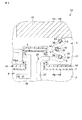
次に、表示ユニット3に設けられる突起部31について詳しく説明する。なお、本体2に設けられる突起部は、表示ユニット3に設けられる突起部31とその構成および機能が同じであるので、同一の符号を付してその説明を省略する。
Next, the
図2に示すように、突起部31は、液晶表示モジュール15とヒンジ部4との間であって、ハーネス21の通り道に設けられている。突起部31は、それぞれ後壁14bの内壁14baから突出する第1ないし第3の突起32,33,34を有する。第1ないし第3の突起32〜34は、ハウジングベース12と一体に円筒状に形成されている。
As shown in FIG. 2, the
第1の突起32、第2の突起33、および第3の突起34は、互いに段違いになるようにして例えば2列に配列される。すなわち第1ないし第3の突起32〜34は、千鳥形状に配置される。第1の突起32と第2の突起33との間の隙間の一例は、ハーネス21の被膜シールド26の外径と略同じである。第3の突起34と第2の突起33との間の隙間の一例は、ハーネス21の被膜シールド26の外径と略同じである。
The
図2および図3に示すように、第1ないし第3の突起32,33,34は、それぞれその側面S(すなわち周面)に導体層35を有する。導体層35は、例えば第2のグランド層17と一体にメッキで形成され、第2のグランド層17に電気的に接続されている。ただし導体層35は、第2のグランド層17に電気的に接続されていれば、第2のグランド層17とは別に形成されたものであっても良い。
As shown in FIGS. 2 and 3, each of the first to
第1ないし第3の突起32,33,34は、少なくともその中の一つが導体層35を有すれば良い。第1ないし第3の突起32,33,34は、表面に導体層35を有する代わりに、突起自体が例えば金属のような導体材料で形成されていても良い。
It is sufficient that at least one of the first to
図2に示すように、突起部31を通過する部位のハーネス21は、絶縁膜27を有さず、被膜シールド26が露出されている。液晶表示モジュール15から延びるハーネス21は、その胴体部を第1ないし第3の突起32,33,34に引っ掛けられ、第1ないし第3の突起32,33,34をガイドにして引き回されている。
As shown in FIG. 2, the
ハーネス21は、第1の突起32と第2の突起33との間を通り、さらに第3の突起34と第2の突起33との間を通るようにして取り付けられる。ハーネス21は、第1および第2の突起32,33の間、および第2および第3の突起33,34の間で挟持され、その位置が固定される。ハーネス21は、千鳥状に形成された第1ないし第3の突起32,33,34によって蛇行した状態で支持される。ヒンジ部4内に延びたハーネス21は、わずかに撓ませてあそびを持たせてある。
The
次に、ポータブルコンピュータ1の作用について説明する。
ハーネス21が第1ないし第3の突起32,33,34により挟持されることで、ハーネス21の被膜シールド26が第1ないし第3の突起32,33,34の導体層35に接する。被膜シールド26は、導体層35を介して第2のグランド層17にアースされる。被膜シールド26がアースされることで、ポータブルコンピュータ1内での電磁波の発生が抑制される。
Next, the operation of the
The
一方、本体2内に延びるハーネス21の被膜シールド26は、本体筐体8に設けられる突起部31により挟持され、第1のグランド層10にアースされる。すなわち、第1および第2のグランド層10,17がハーネス21の被膜シールド26を介して互いに導通し、それぞれの電位が同じになる。これにより、2つのグランド層10,17の電位差に起因する妨害電磁波の発生が抑制される。
On the other hand, the
このようなポータブルコンピュータ1によれば、筐体8,14に取り付けられる別部材を設けることなく、ハーネス21の被膜をアースすることができる。すなわち、側面Sに導体層35を有する突起32,33,34を設けるとともにハーネス21をこの突起32,33,34に絡めて配線することで、被膜シールド26がアースされる。つまり、ハーネス21を第2のグランド層17に押し付ける別部材や、被膜シールド26に別途取り付けられるアース線などが不要である。
According to such a
したがって、従来に比べて小さなスペースでアース構造を達成することができ、小型化を図ったポータブルコンピュータ1を得ることができる。さらに、別部材が不要であるのでコストダウンを図ったポータブルコンピュータ1を得ることができる。被膜シールド26のアースは、ハーネス21を突起32,33,34の間に挟み込むことで達成される。すなわち別部材を取り付ける手間が省略され、組立作業性の向上を図ったポータブルコンピュータ1を得ることができる。
Therefore, the ground structure can be achieved in a smaller space than in the prior art, and the
特に、第1ないし第3の突起32,33,34がハーネス21を蛇行させて支持すると、ハーネス21がより強固に突起間で保持され、被膜シールド26が確実にアースされる。
導体層35を有する突起は少なくとも一つあれば良いが、複数の突起が導体層35を有することで、より低い電気抵抗値でグランド接続が達成される。
In particular, when the first to
At least one protrusion having the
第1ないし第3の突起32,33,34の形状は、円筒状に限られず、例えばハーネス21に沿った壁状のものでも良い。ただし突起のなかでハーネス21に接する面が曲面形状に形成されていると、被膜シールド26と導体層35との接触面積が増加し、より低い電気抵抗値でグランド接続が達成される。
The shape of the first to
なお、突起の数は3つに限らず、2つでも良いし4つ以上であっても良い。突起の配列も千鳥形状に限らず、適宜選択することができる。 The number of protrusions is not limited to three, but may be two or four or more. The arrangement of the protrusions is not limited to the staggered shape, and can be appropriately selected.
次に、本発明の第2の実施形態に係る電子機器としてのポータブルコンピュータ41を、図4を参照して説明する。なお、第1の実施形態に係るポータブルコンピュータ1と同じ機能を有する構成は、同一の符号を付してその説明を省略する。
ポータブルコンピュータ41は突起部42を有する。突起部42の第1および第3の突起32,34は、それぞれその頭頂部に開口するねじ穴43を有する。ねじ穴43は、係合穴の一例である。
Next, a
The
ポータブルコンピュータ41のハウジングカバー13は、第1および第2のボス44,45を有する。第1のボス44は、前壁14aから第1の突起32を向いて延びており、第1の突起32に対向している。第2のボス45は、前壁14aから第3の突起34を向いて延びており、第3の突起34に対向している。
The
第1および第2のボス44,45は、それぞれ筐体8の外部に開口するとともにねじ穴43に連通する孔46を有する。ハウジングカバー13がハウジングベース12に組み合わされた状態で、第1および第2のボス44,45の孔46にはねじ47が挿入される。ねじ47は、固定部材の一例である。ねじ47の先端は、ねじ穴43に係合する。これにより、ハウジングカバー13とハウジングベース12とが互いに固定される。換言すれば、第1および第3の突起32,34は、ディスプレイハウジング14の固定用のボスであり、このボスを利用してハーネス21がアースされる。
The first and
このようなポータブルコンピュータ41によれば、突起32,33,34の導体層35を介してハーネス21の被膜シールド26がアースされるので、アース用の別部材を設ける必要がない。これにより、小型化、コストダウンおよび組立作業性の向上を図ったポータブルコンピュータ41を得ることができる。
According to such a
特に本実施形態に係るポータブルコンピュータ41のように、第1および第3の突起32,34をねじ止め用のボスと兼用することで、アース構造が必要とするスペースの省略または縮小、およびポータブルコンピュータ41のコストダウンをさらに図ることができる。
In particular, as in the
なお、本実施形態では2つの突起32,34がねじ止め用のボスであったが、ねじ止め用のボスと兼用される突起は1つでも良く、また全ての突起が兼用されても良い。
In this embodiment, the two
次に、本発明の第3の実施形態に係る電子機器としてのポータブルコンピュータ51を、図5および図6を参照して説明する。なお、第1の実施形態に係るポータブルコンピュータ1と同じ機能を有する構成は、同一の符号を付してその説明を省略する。
Next, a
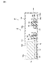
ポータブルコンピュータ51は突起部52を有する。図5および図6に示すように、突起部52は、ハーネス21の通り道に設けられている。突起部52は、それぞれ後壁14bの内壁14baから突出する第1ないし第3の突起53,54,55を有する。
The
第1の突起53、第2の突起54、第3の突起55は、互いに段違いになるようにして例えば2列に配列される。すなわち第1ないし第3の突起53〜55は、千鳥形状に配置される。第1の突起53と第2の突起54との間の隙間の一例は、ハーネス21の被膜シールド26の外径に比べて大きい。第3の突起55と第2の突起54との間の隙間の一例は、ハーネス21の被膜シールド26の外径に比べて大きい。第1ないし第3の突起53,54,55は、それぞれその側面Sに導体層35を有する。
The
図5に示すように、ハーネス21は、その胴体部の左右両側面が第1ないし第3の突起53,54,55に交互に引っ掛けられ、第1ないし第3の突起53,54,55をガイドにして引き回されている。ハーネス21は、各突起53,54,55の側面Sに沿って引き回され、それぞれの側面Sに巻き付くようにして突起53,54,55に絡んで延びている。
As shown in FIG. 5, the left and right side surfaces of the harness portion of the
さらに具体的に述べると、第1ないし第3の突起53,54,55は図5中で左右の2列に分かれて配置されている。ハーネス21は、右列に位置する第1および第3の突起53,55の右側面に沿うとともに、左列に位置する第2の突起54の左側面に沿って延びている。すなわちハーネス21は、突起部52の外周部位に位置する側面を辿るように延びている。
ハーネス21は、千鳥状に形成された第1ないし第3の突起53,54,55に左右の両側面を交互に支持され、蛇行した状態に保たれる。
More specifically, the first to
The
なお、ハーネス21は、右列に位置する突起の左側面と左列に位置する突起の右側面に沿う、すなわち図2に示すように突起部52の内周部位に位置する側面を辿るように延びていても良い。
The
なお、第1ないし第3の突起53,54,55の形状は、円筒状に限られず、例えばハーネス21に沿った壁状のものでも良い。ただし突起のなかでハーネス21に接する面が曲面形状に形成されていると、より低い電気抵抗値でグランド接続が達成される。
The shape of the first to
次に、ポータブルコンピュータ51の作用について説明する。
第1ないし第3の突起53,54,55の互いの間の隙間がハーネス21より太いことから、ハーネス21は、第1ないし第3の突起部53,54,55によって固定されない。ここで、ハーネス21はヒンジ部4を通じて本体2内にも延びていることから、表示ユニット3の開閉に伴なって伸びたり屈曲したりする。ハーネス21は、表示ユニット3の開閉に伴なって多少その位置が動く。
Next, the operation of the
Since the gap between the first to
しかし、ハーネス21の左右両側面が突起53,54,55のいずれかに接するように絡んでいることから、ハーネス21はその位置が多少ずれても少なくとも1つの突起に接触した状態を保つ。ハーネス21が突起53,54,55の少なくとも一つと接触を保つことで、被膜シールド26は常に第2のグランド層17にアースされる。
However, since the left and right side surfaces of the
このようなポータブルコンピュータ51によれば、突起53,54、55の導体層35を介してハーネス21の被膜シールド26がアースされるので、アース用の別部材を設ける必要がない。被膜シールド26をアースは、ハーネス21を突起53,54,55に絡めることで達成される。これにより、小型化、コストダウンおよび組立作業性の向上を図ったポータブルコンピュータ51を得ることができる。
According to such a
なお、突起の数は3つに限らず、2つでも良いし4つ以上であっても良い。突起の配列も千鳥形状に限られない。 The number of protrusions is not limited to three, but may be two or four or more. The arrangement of the protrusions is not limited to the staggered shape.
次に、本発明の第4の実施形態に係る電子機器としてのポータブルコンピュータ61を、図7および図8を参照して説明する。なお、第1および第3の実施形態に係るポータブルコンピュータ1,51と同じ機能を有する構成は、同一の符号を付してその説明を省略する。
Next, a
ポータブルコンピュータ61は突起部62を有する。突起部62の第1ないし第3の突起53,54,55は、それぞれハウジングベース12から突出した突起本体63と、突起本体63の突出端から内壁14baに平行に延びる延伸部64とを有する。すなわち、第1ないし第3の突起52,53,54は、鉤爪形状に形成されている。延伸部64は、突起本体63からハーネス21を覆う方向に延びている。
The
このようなポータブルコンピュータ61によれば、突起53,54,55の導体層35を介してハーネス21の被膜シールド26がアースされるので、アース用の別部材を設ける必要がない。これにより、小型化、コストダウンおよび組立作業性の向上を図ったポータブルコンピュータ61を得ることができる。
According to such a
特に第1ないし第3の突起53,54,55が鉤爪状に形成されていると、ハーネス21が突起部62から外れにくくなる。これにより、さらに確実に被膜シールド26のアースを達成することができる。
In particular, when the first to
次に、本発明の第5の実施形態に係る電子機器としてのポータブルコンピュータ71を、図9を参照して説明する。なお、第1ないし第3の実施形態に係るポータブルコンピュータ1,41,51と同じ機能を有する構成は、同一の符号を付してその説明を省略する。
Next, a
ポータブルコンピュータ71は突起部72を有する。突起部72の第1および第3の突起53,55は、それぞれ頭頂部にねじ穴43を有する。換言すれば、第1および第3の突起53,55は、ディスプレイハウジング14の固定用のボスであり、このボスを兼用してハーネス21がアースされる。
The
このようなポータブルコンピュータ71によれば、突起53,54,55の導体層35を介してハーネス21の被膜シールド26がアースされるので、アース用の別部材を設ける必要がない。さらに第2の実施形態と同様に、より小型化、コストダウンおよび組立作業性の向上を図ったポータブルコンピュータ71を得ることができる。
According to such a
以上、第1ないし第5の実施形態に係るポータブルコンピュータ1,41,51,61,71について説明したが、本発明はこれらに限定されるものではない。例えば、第1ないし第3の突起32〜34,53〜55の形状は特に限定されるものではなく、楕円形状や多角形状など適宜選択して用いることができる。被膜シールド26は、第1および第2のグランド層10,17を同電位にする導体被膜である必要は無く、他の目的で設けられるものであっても良い。
The
なお、第2および5の実施形態に係るポータブルコンピュータ41,71では、突起32,34,53,55に係合穴43が設けられ、ボス44,45に孔46が設けられている。これに代えて突起32,34,53,55に孔46を設けるとともに、ボス44,45に係合穴43を設けても良い。この場合ねじ47は、ハウジングベース12に設けられた孔46を通じてハウジングカバー13の係合穴43に係合される。
In the
ハーネス21は、液晶表示モジュール15用に限らず、例えば複数の回路基板同士を接続するものであっても良く、その種類は問わない。本発明の実施形態が適用可能な電子機器はポータブルコンピュータに限らず、携帯電話、デジタルカメラ、ビデオカメラ、またはパーソナルデジタルアシスタントのようなあらゆる電子機器に適用可能である。
The
1…ポータブルコンピュータ、2…本体、3…表示ユニット、12…ハウジングベース、13…ハウジングカバー、14…ディスプレイハウジング、14ba…内壁、15…液晶表示モジュール、17…第2のグランド層、21…ハーネス、26…被膜シールド、31…突起部、32〜34突起、35…導体層、41…ポータブルコンピュータ、42…突起部、43…ねじ穴、44…第1のボス、45…第2のボス、47…ねじ、51…ポータブルコンピュータ、52…突起部、53〜55…突起。
DESCRIPTION OF
Claims (9)
第2の筐体と、
上記第1の筐体と上記第2の筐体とを回動可能に連結したヒンジ部と、
上記第2の筐体に収容されたモジュールと、
上記モジュールに電気的に接続され、上記ヒンジ部を通って上記第2の筐体と上記第1の筐体とに延びるとともに、導電性の被膜を有したケーブルと、
上記第2の筐体内に設けられたグランド層と、
上記ヒンジ部と連結された上記第2の筐体の端部に設けられ、上記第2の筐体の内壁から突出した複数の突起であって、少なくともそのうち1つの突起は側面に上記グランド層に電気的に接続されるとともに上記ケーブルの導電性の被膜に接した導体層を有し、該突起と他の突起との間に配線された上記ケーブルを挟持した複数の突起と、
を具備したことを特徴とする電子機器。 A first housing;
A second housing;
A hinge portion rotatably connecting the first housing and the second housing;
A module housed in the second housing;
A cable electrically connected to the module, extending through the hinge portion to the second housing and the first housing, and having a conductive coating;
A ground layer provided in the second housing;
A plurality of protrusions provided at an end of the second casing connected to the hinge portion and protruding from an inner wall of the second casing, at least one of the protrusions on a side surface of the ground layer; A plurality of protrusions having a conductor layer that is electrically connected and in contact with the conductive coating of the cable, sandwiching the cable wired between the protrusion and another protrusion;
An electronic apparatus comprising:
上記第1の筐体に収容された他のモジュールと、
上記第1の筐体内に設けられた他のグランド層と、
上記ヒンジ部に連結された上記第1の筐体の端部に設けられ、上記第1の筐体の内壁から突出した他の複数の突起であって、少なくともそのうち1つの突起は側面に上記他のグランド層に電気的に接続されるとともに上記ケーブルの導電性の被膜に接した導体層を有し、該突起と他の突起との間に配線された上記ケーブルを挟持した複数の突起と、を備え、
上記ケーブルは、上記他のモジュールに接続され、上記ケーブルを介して上記モジュールと上記他のモジュールとが電気的に接続されるとともに、上記ケーブルの導電性の被膜を介して上記グランド層と上記他のグランド層とが電気的に接続されたことを特徴とする電子機器。 The electronic device according to claim 1,
Another module housed in the first housing;
Another ground layer provided in the first housing;
A plurality of other projections provided at an end of the first casing connected to the hinge portion and projecting from an inner wall of the first casing, at least one of the projections on the side surface of the other casing A plurality of protrusions sandwiching the cable wired between the protrusions and the other protrusions, having a conductor layer that is electrically connected to the ground layer and in contact with the conductive coating of the cable, With
The cable is connected to the other module, the module and the other module are electrically connected via the cable, and the ground layer and the other are connected via a conductive coating of the cable. An electronic device characterized by being electrically connected to the ground layer.
上記複数の突起の全てが、上記導体層を有したことを特徴とする電子機器。 The electronic device according to claim 2,
All of the plurality of protrusions have the conductor layer.
上記突起は、少なくとも上記ケーブルに接する面が曲面状であることを特徴とする電子機器。 The electronic device according to claim 3,
The electronic device according to claim 1, wherein at least a surface of the protrusion contacting the cable is a curved surface.
上記第2の筐体は、上記突起が設けられた第1のハウジング部材と、上記第1のハウジング部材に組み合わされた第2のハウジング部材と、上記第2のハウジング部材を上記第1のハウジング部材に固定した固定部材とを有し、
上記突起は、上記第2のハウジング部材に組み付けられた上記固定部材が係合する係合穴が設けられたことを特徴とする電子機器。 The electronic device according to claim 4,
The second housing includes a first housing member provided with the protrusion, a second housing member combined with the first housing member, and the second housing member as the first housing. A fixing member fixed to the member,
The electronic apparatus according to claim 1, wherein the protrusion is provided with an engagement hole with which the fixing member assembled to the second housing member is engaged.
第2の筐体と、
上記第1の筐体と上記第2の筐体とを回動可能に連結したヒンジ部と、
上記第2の筐体に収容されたモジュールと、
上記第2の筐体内に設けられたグランド層と、
上記ヒンジ部に連結された上記第2の筐体の端部に設けられ、上記第2の筐体の内壁から突出するとともに、側面に上記グランド層に電気的に接続された導体層を有した複数の突起と、
上記モジュールに電気的に接続され、上記ヒンジ部を通って上記第2の筐体と上記第1の筐体とに延び、上記突起の導体層に接した導電性の被膜を有し、上記各突起の側面に沿って引き回され、上記突起に絡んで延びたケーブルと、
を具備したことを特徴とする電子機器。 A first housing;
A second housing;
A hinge portion rotatably connecting the first housing and the second housing;
A module housed in the second housing;
A ground layer provided in the second housing;
Provided at the end of the second casing connected to the hinge portion, and protruding from the inner wall of the second casing, and having a conductor layer electrically connected to the ground layer on the side surface A plurality of protrusions;
Electrically connected to the module, extending through the hinge portion to the second casing and the first casing, and having a conductive coating in contact with the conductor layer of the protrusion, A cable that is routed along the side surface of the projection and extends around the projection;
An electronic apparatus comprising:
上記複数の突起は、互いの間に上記ケーブルの太さより大きな間隔を空けて配置されたことを特徴とする電子機器。 The electronic device according to claim 6,
The electronic device according to claim 1, wherein the plurality of protrusions are arranged with a gap larger than the thickness of the cable between them.
上記突起は、少なくとも上記ケーブルに接する面が曲面状であることを特徴とする電子機器。 The electronic device according to claim 7,
The electronic device according to claim 1, wherein at least a surface of the protrusion contacting the cable is a curved surface.
上記第2の筐体は、上記突起が設けられた第1のハウジング部材と、上記第1のハウジング部材に組み合わされた第2のハウジング部材と、上記第2のハウジング部材を上記第1のハウジング部材に固定した固定部材とを有し、
上記突起は、上記第2のハウジング部材に組み付けられた上記固定部材が係合する係合穴が設けられたことを特徴とする電子機器。 The electronic device according to claim 8,
The second housing includes a first housing member provided with the protrusion, a second housing member combined with the first housing member, and the second housing member as the first housing. A fixing member fixed to the member,
The electronic apparatus according to claim 1, wherein the protrusion is provided with an engagement hole with which the fixing member assembled to the second housing member is engaged.
Priority Applications (4)
| Application Number | Priority Date | Filing Date | Title |
|---|---|---|---|
| JP2006050600A JP4762002B2 (en) | 2006-02-27 | 2006-02-27 | Electronics |
| US11/644,636 US7952886B2 (en) | 2006-02-27 | 2006-12-21 | Electronic apparatus |
| CNA200610172001XA CN101031188A (en) | 2006-02-27 | 2006-12-26 | Electronic apparatus |
| US13/109,841 US8514589B2 (en) | 2006-02-27 | 2011-05-17 | Electronic apparatus |
Applications Claiming Priority (1)
| Application Number | Priority Date | Filing Date | Title |
|---|---|---|---|
| JP2006050600A JP4762002B2 (en) | 2006-02-27 | 2006-02-27 | Electronics |
Publications (2)
| Publication Number | Publication Date |
|---|---|
| JP2007234630A JP2007234630A (en) | 2007-09-13 |
| JP4762002B2 true JP4762002B2 (en) | 2011-08-31 |
Family
ID=38444588
Family Applications (1)
| Application Number | Title | Priority Date | Filing Date |
|---|---|---|---|
| JP2006050600A Expired - Fee Related JP4762002B2 (en) | 2006-02-27 | 2006-02-27 | Electronics |
Country Status (3)
| Country | Link |
|---|---|
| US (2) | US7952886B2 (en) |
| JP (1) | JP4762002B2 (en) |
| CN (1) | CN101031188A (en) |
Families Citing this family (20)
| Publication number | Priority date | Publication date | Assignee | Title |
|---|---|---|---|---|
| JP2009277728A (en) * | 2008-05-12 | 2009-11-26 | Mitsumi Electric Co Ltd | Cable fixation structure, and electronic apparatus |
| BRPI0822541A2 (en) * | 2008-07-25 | 2015-06-23 | Hewlett Packard Development Co | Computing device, laptop, and leakage current dissipating device for use with a laptop |
| CN101997284A (en) * | 2009-08-20 | 2011-03-30 | 鸿富锦精密工业(深圳)有限公司 | Fixed cable tie |
| JP2011211188A (en) * | 2010-03-11 | 2011-10-20 | Panasonic Corp | Electronic device |
| TWI433637B (en) * | 2010-07-02 | 2014-04-01 | 瀚宇彩晶股份有限公司 | Double-sided cable structure and electronic device with double-sided cable structure |
| CN102387674A (en) * | 2010-08-30 | 2012-03-21 | 鸿富锦精密工业(深圳)有限公司 | Electronic device |
| JP4929405B1 (en) * | 2011-02-14 | 2012-05-09 | 株式会社東芝 | Electronics |
| US8710376B2 (en) * | 2011-08-31 | 2014-04-29 | Apple Inc. | Systems of an electronic device and methods for manufacturing the same |
| EP2645490B1 (en) * | 2011-11-09 | 2018-01-03 | Fuji Electric Wire Industries CO., LTD. | Electrical wire wiring structure for plug |
| US9182794B2 (en) * | 2011-11-30 | 2015-11-10 | Google Inc. | Notebook metal hinge as heat sink element |
| CN103458668A (en) * | 2012-05-29 | 2013-12-18 | 鸿富锦精密工业(深圳)有限公司 | Electromagnetic interference preventing component and electronic device with same |
| US8982582B2 (en) * | 2012-11-30 | 2015-03-17 | Apple Inc. | Electronic device with antenna cable bracket |
| US9624706B2 (en) * | 2012-12-17 | 2017-04-18 | Hewlett-Packard Development Company, L.P. | Hinge assembly |
| JP6323250B2 (en) * | 2014-08-15 | 2018-05-16 | 富士通株式会社 | Electronic device and method for manufacturing electronic device |
| JP6446324B2 (en) * | 2015-04-28 | 2018-12-26 | シャープ株式会社 | Housing, display device, and television receiver |
| JP6788185B2 (en) * | 2016-09-21 | 2020-11-25 | 富士通クライアントコンピューティング株式会社 | Electronic devices and restricted parts |
| CN110214452B (en) * | 2017-01-31 | 2022-01-18 | 三菱电机株式会社 | Operating device |
| US10224670B2 (en) * | 2017-07-17 | 2019-03-05 | Facebook Technologies, Llc | Circuit board with anchor cleat for a connector |
| JP6785444B1 (en) * | 2020-02-06 | 2020-11-18 | パナソニックIpマネジメント株式会社 | Information processing device |
| US20250106995A1 (en) * | 2023-09-27 | 2025-03-27 | Apple Inc. | Compact interface through hinge connector |
Family Cites Families (45)
| Publication number | Priority date | Publication date | Assignee | Title |
|---|---|---|---|---|
| US269268A (en) * | 1882-12-19 | Fire-escape | ||
| US3810186A (en) * | 1968-01-31 | 1974-05-07 | Sumitomo Electric Industries | Leaky coaxial cable |
| US3676836A (en) * | 1970-10-01 | 1972-07-11 | George W Gillemot | Universal sheath bond for communications cable |
| US4181384A (en) * | 1978-02-06 | 1980-01-01 | Amp Incorporated | Flat cable connector having wire deployment means |
| JPS5832327U (en) * | 1981-08-19 | 1983-03-02 | 三菱電機株式会社 | Karman vortex flowmeter |
| JPS59115684A (en) | 1982-12-22 | 1984-07-04 | Pioneer Electronic Corp | System for preventing interception in catv system |
| JPS59115684U (en) * | 1983-01-26 | 1984-08-04 | 株式会社チノ− | electronic equipment housing |
| IL71719A (en) * | 1984-05-02 | 1992-08-18 | Dan Marom | Rescue and glider device |
| US5379439A (en) * | 1985-06-04 | 1995-01-03 | Quantum Corporation | Fixed disk drive mounted to printed circuit board |
| US4701139A (en) * | 1986-04-25 | 1987-10-20 | Amp Incorporated | Shielded cable assembly |
| JPH0686859B2 (en) | 1986-07-01 | 1994-11-02 | 日本電装株式会社 | Glow plug energization control device |
| JPS6312884U (en) * | 1986-07-11 | 1988-01-27 | ||
| US4980062A (en) | 1988-09-16 | 1990-12-25 | W. R. Grace & Co.-Conn. | Inorganic membrane |
| JPH0710416Y2 (en) * | 1989-01-12 | 1995-03-08 | 沖電気工業株式会社 | Electronic device cable cover structure |
| JPH04169917A (en) * | 1990-05-07 | 1992-06-17 | Toshiba Corp | Portable electronic apparatus |
| US5566050A (en) * | 1992-07-17 | 1996-10-15 | Kabushiki Kaisha Toshiba | Compact electronic apparatus having a detachable optional component |
| US5552967A (en) * | 1993-04-30 | 1996-09-03 | Kabushiki Kaisha Toshiba | Portable electronic apparatus having a housing for containing circuits board and functional components |
| JPH0713660A (en) * | 1993-06-21 | 1995-01-17 | Toshiba Corp | Portable electronic devices |
| US5952616A (en) * | 1995-09-22 | 1999-09-14 | Hughes Electronics Corporation | Cable retainer with retaining surfaces having offset protrusions |
| US5911595A (en) * | 1996-07-29 | 1999-06-15 | Kern Engineering & Mfg. Co. | Low profile angular connector device and method |
| JPH10268976A (en) * | 1997-03-27 | 1998-10-09 | Toshiba Corp | Portable electronic devices |
| US6047660A (en) * | 1997-09-06 | 2000-04-11 | Lee; Brent W. | Apparatus and method to form coated shielding layer for coaxial signal transmission cables |
| US5989042A (en) * | 1998-04-03 | 1999-11-23 | 23-3178 | Electrical connector for use between shielded media connectors and computer communications cards |
| JP2000151140A (en) * | 1998-11-06 | 2000-05-30 | Matsushita Electric Ind Co Ltd | Hinge with electric wire guide and electronic equipment |
| CA2265175A1 (en) * | 1999-03-11 | 2000-09-11 | Newbridge Networks Corporation | A latching device for a circuit pack |
| DE29904944U1 (en) * | 1999-03-18 | 1999-06-24 | Fritschle, Simone, 70195 Stuttgart | Multiple cables |
| JP2001147441A (en) * | 1999-11-19 | 2001-05-29 | Nec Corp | Transverse electric field liquid crystal display device |
| US6315249B1 (en) * | 1999-12-29 | 2001-11-13 | Dell Usa, L.P. | System for managing cables for a rack-mounted computer system |
| US6540312B1 (en) * | 2000-02-25 | 2003-04-01 | Telica, Inc. | Cable guide system |
| US6466728B1 (en) * | 2000-03-08 | 2002-10-15 | Marconi Communications, Inc. | Attenuator for fiber optic cables |
| US6625849B1 (en) * | 2000-10-31 | 2003-09-30 | Marconi Communications, Inc. | Cable strain relief |
| US6900383B2 (en) * | 2001-03-19 | 2005-05-31 | Hewlett-Packard Development Company, L.P. | Board-level EMI shield that adheres to and conforms with printed circuit board component and board surfaces |
| JP2002299851A (en) * | 2001-03-29 | 2002-10-11 | Mitsubishi Electric Corp | Cable clamp structure |
| US6481662B1 (en) * | 2001-07-26 | 2002-11-19 | Ciena Corporation | Fiber optic cable winding assist tool |
| JP3603831B2 (en) | 2001-10-10 | 2004-12-22 | ダイキン工業株式会社 | Electrical component box and air conditioner |
| US6617518B2 (en) * | 2001-11-02 | 2003-09-09 | Jds Uniphase Corporaton | Enhanced flex cable |
| JP4194019B2 (en) * | 2002-06-28 | 2008-12-10 | Fdk株式会社 | Signal transmission cable with connector |
| JP2004232782A (en) * | 2003-01-31 | 2004-08-19 | Canon Inc | Hinge device |
| US7000784B2 (en) * | 2003-03-07 | 2006-02-21 | Panduit Corp. | Rack-mountable cable manager |
| DE10328956A1 (en) * | 2003-06-27 | 2005-01-20 | Elmotec Statomat Vertriebs Gmbh | Method and device for introducing wave windings in rotor and stator lamination packages of electrical machines |
| JP2005070969A (en) * | 2003-08-21 | 2005-03-17 | Toshiba Corp | Electronic device and operation unit used for electronic device |
| US20060070809A1 (en) * | 2004-09-30 | 2006-04-06 | Yoav Barzilai | Advanced "Omer" rescue system |
| JP2006129676A (en) * | 2004-11-01 | 2006-05-18 | Fuji Xerox Co Ltd | Method of terminating shielded cable, terminal shielding structure, and light transmitting/receiving system using terminal shielding structure |
| JP4633605B2 (en) * | 2005-01-31 | 2011-02-16 | 富士通コンポーネント株式会社 | ANTENNA DEVICE AND ELECTRONIC DEVICE, ELECTRONIC CAMERA, ELECTRONIC CAMERA LIGHT EMITTING DEVICE, AND PERIPHERAL DEVICE |
| US7359609B2 (en) * | 2005-06-14 | 2008-04-15 | Scientific-Atlanta, Inc. | Storage trough and fiber management system |
-
2006
- 2006-02-27 JP JP2006050600A patent/JP4762002B2/en not_active Expired - Fee Related
- 2006-12-21 US US11/644,636 patent/US7952886B2/en not_active Expired - Fee Related
- 2006-12-26 CN CNA200610172001XA patent/CN101031188A/en active Pending
-
2011
- 2011-05-17 US US13/109,841 patent/US8514589B2/en active Active
Also Published As
| Publication number | Publication date |
|---|---|
| US20070202743A1 (en) | 2007-08-30 |
| US8514589B2 (en) | 2013-08-20 |
| US20110216509A1 (en) | 2011-09-08 |
| CN101031188A (en) | 2007-09-05 |
| JP2007234630A (en) | 2007-09-13 |
| US7952886B2 (en) | 2011-05-31 |
Similar Documents
| Publication | Publication Date | Title |
|---|---|---|
| JP4762002B2 (en) | Electronics | |
| JP5584086B2 (en) | Electronics | |
| JP3066802B1 (en) | Hinge connector | |
| JP4945337B2 (en) | Electronics | |
| JP4892050B2 (en) | Electronics | |
| JP6715973B1 (en) | Electronics | |
| JP4477082B2 (en) | Electronics | |
| JP4153951B2 (en) | Thin display device and plasma display | |
| CN101331743A (en) | wire support device | |
| JP6022034B2 (en) | Electronics | |
| JP5022800B2 (en) | Electronics | |
| JP2011129706A (en) | Electronic apparatus | |
| JP2010011405A (en) | Electronic apparatus | |
| JP2007287541A (en) | Cable harness | |
| JP4754410B2 (en) | Portable electronic devices | |
| JP5257326B2 (en) | Portable terminal | |
| JP5609653B2 (en) | Electronics | |
| US20130321708A1 (en) | Television receiver and electronic device | |
| JP5150761B1 (en) | Electronics | |
| JP2006338970A (en) | Connector device, circuit board, electronic equipment | |
| JP5058369B2 (en) | Electronics | |
| JP2005259598A (en) | Micro coaxial cable assembly and terminal structure of micro coaxial cable assembly | |
| JP4019356B2 (en) | Shield structure | |
| JP2007287439A (en) | Cable harness | |
| TWI394324B (en) | The connector |
Legal Events
| Date | Code | Title | Description |
|---|---|---|---|
| A621 | Written request for application examination |
Free format text: JAPANESE INTERMEDIATE CODE: A621 Effective date: 20080522 |
|
| A977 | Report on retrieval |
Free format text: JAPANESE INTERMEDIATE CODE: A971007 Effective date: 20101126 |
|
| A131 | Notification of reasons for refusal |
Free format text: JAPANESE INTERMEDIATE CODE: A131 Effective date: 20101130 |
|
| A521 | Request for written amendment filed |
Free format text: JAPANESE INTERMEDIATE CODE: A523 Effective date: 20110128 |
|
| A131 | Notification of reasons for refusal |
Free format text: JAPANESE INTERMEDIATE CODE: A131 Effective date: 20110308 |
|
| A521 | Request for written amendment filed |
Free format text: JAPANESE INTERMEDIATE CODE: A523 Effective date: 20110415 |
|
| TRDD | Decision of grant or rejection written | ||
| A01 | Written decision to grant a patent or to grant a registration (utility model) |
Free format text: JAPANESE INTERMEDIATE CODE: A01 Effective date: 20110510 |
|
| A61 | First payment of annual fees (during grant procedure) |
Free format text: JAPANESE INTERMEDIATE CODE: A61 Effective date: 20110607 |
|
| FPAY | Renewal fee payment (event date is renewal date of database) |
Free format text: PAYMENT UNTIL: 20140617 Year of fee payment: 3 |
|
| R151 | Written notification of patent or utility model registration |
Ref document number: 4762002 Country of ref document: JP Free format text: JAPANESE INTERMEDIATE CODE: R151 |
|
| FPAY | Renewal fee payment (event date is renewal date of database) |
Free format text: PAYMENT UNTIL: 20140617 Year of fee payment: 3 |
|
| S111 | Request for change of ownership or part of ownership |
Free format text: JAPANESE INTERMEDIATE CODE: R313121 Free format text: JAPANESE INTERMEDIATE CODE: R313117 |
|
| R350 | Written notification of registration of transfer |
Free format text: JAPANESE INTERMEDIATE CODE: R350 |
|
| LAPS | Cancellation because of no payment of annual fees |