JP4761487B2 - Bus architecture and information processing apparatus using the same - Google Patents
Bus architecture and information processing apparatus using the same Download PDFInfo
- Publication number
- JP4761487B2 JP4761487B2 JP2000131103A JP2000131103A JP4761487B2 JP 4761487 B2 JP4761487 B2 JP 4761487B2 JP 2000131103 A JP2000131103 A JP 2000131103A JP 2000131103 A JP2000131103 A JP 2000131103A JP 4761487 B2 JP4761487 B2 JP 4761487B2
- Authority
- JP
- Japan
- Prior art keywords
- module
- modules
- bus
- pixel
- address
- Prior art date
- Legal status (The legal status is an assumption and is not a legal conclusion. Google has not performed a legal analysis and makes no representation as to the accuracy of the status listed.)
- Expired - Fee Related
Links
Images


Classifications
-
- G—PHYSICS
- G06—COMPUTING; CALCULATING OR COUNTING
- G06F—ELECTRIC DIGITAL DATA PROCESSING
- G06F13/00—Interconnection of, or transfer of information or other signals between, memories, input/output devices or central processing units
- G06F13/38—Information transfer, e.g. on bus
- G06F13/42—Bus transfer protocol, e.g. handshake; Synchronisation
- G06F13/4247—Bus transfer protocol, e.g. handshake; Synchronisation on a daisy chain bus
- G06F13/4256—Bus transfer protocol, e.g. handshake; Synchronisation on a daisy chain bus using a clocked protocol
Landscapes
- Engineering & Computer Science (AREA)
- Theoretical Computer Science (AREA)
- Physics & Mathematics (AREA)
- General Engineering & Computer Science (AREA)
- General Physics & Mathematics (AREA)
- Bus Control (AREA)
- Debugging And Monitoring (AREA)
- Tests Of Electronic Circuits (AREA)
Description
【0001】
【発明の分野】
本発明はバスアーキテクチャに関し、特に、ハードウェア、特に集積回路に適用して実現した場合に最小限のスペースしか費やさない順次構成に関する。
【0002】
【背景】
この数年間、電子システム内の個々の装置及び/又はモジュールの間で情報を通信することが要求される様々な状況を処理するために、多様なバスアーキテクチャが開発されてきた。あるバスアーキテクチャをどの程度まで利用できるかは、バスにより実現すべきデータ転送速度、データ転送を実行すべき特定の環境、データを転送しなければならない距離などを含むいくつかの要因によって決まる。
【0003】
パーソナルコンピュータなどの計算システムにおいては、通常、バスはマイクロプロセッサ型装置により制御される複数の並列する両方向構成により形成される。状況によっては、複数の装置又はモジュールに1つの直列バスを結合する場合もあるが、これは、個々のモジュールがモジュール間の相互接続の稼働率を感知し、データ送信を利用できるようになった時点で通信リンクの制御を獲得するという動作に依存している。このような構成では、ある回線における「話者」は1人であるが、「聴取者」は多数であるので、1つのモジュールから送信されたデータが所望の宛先モジュールにより確実に受信されるように保証するためには、衝突防止構成を実現することが必要である。上述の構成はプリント回路と、集積回路の双方に適用可能であるが、回路の設計に際しては、どのような特定の実現形態をとるかによって、それぞれ、様々な利点と欠点とをもたらす。
【0004】
集積デバイスが通信を行うことを望むいくつかのモジュールを含み、集積デバイスと関連する1つの外部インタフェースポートを介して通信をチャネリングするような統合型システムにこれを適用する場合には、問題が生じる。そのような構成を図1に示す。図1に示すように、単一の集積デバイス10がその周辺又はその付近に配置された通信モジュール12を含み、これに外部通信リンク14が接続している。デバイス10の内部には複数のモジュール16A〜16Eがあり、通信リンク14からのデータをそれらのモジュールとの間で転送することが望まれている。この転送を容易にするため、通信モジュール12は、対応するモジュール16A〜16Eに至る複数の通信リンク18A〜18Eを含む。これらの通信リンク18A〜18Eは、所期のモジュール16A〜16Eへの通信信号の多重化を行う。通信リンク18A〜18Eは、通常、並列バス構成を有する。図1の構成に類似する構成をプリント回路又はより大規模な回路に適用した場合、プリント回路カード又はシステムの周囲の様々な通信リンクを実現する際の詳細に関しては、電子回路の設計に当たり、ほとんど問題は起こらない。しかし、図示するように、図1の構成を1つの電子チップデバイスに統合した場合には、個々のモジュール16の数が増すと、それに対応してリンク18の数も増やさなければならないため、問題が生じる。集積デバイスの周囲にモジュール16が展開している場合、モジュール16と通信インタフェースモジュール12との間に様々な集積接続及び配線接続を成立させるように集積回路を設計することは、アーキテクチャの上で困難になる。また、集積回路のモジュール12の付近には、通信リンクを都合よく且つ/又は経済的に配置するだけの十分なスペースがない。
【0005】
この問題を解決するための構成の1つを図2に示す。図2に示す通信装置の構成20では、それぞれがバス22に至る対応する配線26A〜26Fを有する複数のモジュール24A〜26Fを互いに接続するリングバスが設けられている。必要に応じて、モジュール24A〜24Fの1つを外部構成との通信を行えるように構成することができ、従って、この構成20はプリント回路と、集積構成の双方に適用可能である。このような構成においては、リングバス22への結合を可能にするために、3状態論理を実現することが要求される。図2の構成の場合、全てがそれぞれ異なる負荷を表している複数のモジュールにリングバス22を接続しなければならず、その結果、デバイス内部で送信の問題が生じ、先に述べたようなコンフリクトを解決することが困難になると考えられるため、この構成を特に集積デバイスに適用するのは問題である。
【0006】
本発明の目的は、上記の問題の1つ又は2つ以上を実質的に克服するか、または少なくとも改善し且つ/又は従来の構成に代わるバスアーキテクチャ構成を提供することである。
【0007】
【発明の概要】
本発明の1つの面によれば、 集積回路デバイスのアクセスポートを介して通信を実行することが望まれる複数のモジュールを具備する集積回路デバイスの内部バスアーキテクチャであって、
各々が前記モジュールのうち2つのモジュールを互いに接続して、前記2つのモジュールの互いに接続された閉ループを形成する複数のバスセグメントと、
各々が前記モジュールのうち対応する1つと関連し、前記閉ループに沿った、前記アクセスポートから前記モジュールの中の宛先モジュールに至る通信トランザクションの単方向転送に少なくとも寄与し且つ前記バスセグメントの数に対応する複数のバスコントローラと、
前記複数のバスセグメントとは別に前記複数のモジュールを接続して処理パイプラインを構成する複数の配線セグメントとを具備し、
前記複数のバスセグメントは、前記処理パイプラインとは別のデバッグ用ループを構成し、
前記複数のモジュールは、
ページ記述言語を入力する映像入力インターフェースと、
受信したページ記述言語から命令を読み取り実行する命令実行部と、
ページ記述言語で記述された図形オブジェクトから取り出されるエッジを読み取り、エッジと走査線の交点を判定するエッジ処理モジュールと、
エッジ間に存在する画素列に対して有効状態で、レンダリングすべき画像に寄与するオブジェクトを判定するレベルアクティベーションモジュールと、
有効画素列を受信しオブジェクトごとの画素の色を判定する画素生成モジュールと、
有効オブジェクトの画素値を優先順位に従って合成し画素値を求めレンダリングする画素合成モジュールと、
レンダリングされた画素を受信し、走査線ごとの画素値を形成する映像出力インターフェースとを含む、前記バスセグメントの数に対応する複数のバスコントローラとを具備するアーキテクチャが開示される。
【0008】
本発明のその他の面も開示される。
【0009】
【詳細な説明】
図3は、本発明の一実施例によるバスアーキテクチャシステムを示す。このバスアーキテクチャシステムは、電子システム(図示せず)とインタフェースできるように構成された通信ポート34を有する集積回路デバイス30の中に形成されている。ポート34は、デバイス30の複数のモジュール36A〜36Eと、それらのモジュール36A〜36Eの連続する2つのモジュールの間に配置された複数の単方向配線38A〜38Fとを含むシーケンシャルバス構成の一部を形成する通信モジュールに接続している。
【0010】
図3には示されていないが、デバイス30がその内外に、様々なモジュール36A〜36Eに接続する複数の別の配線を含んでいても良いことは当業者には理解されるであろう。
【0011】
図3の構成では、通信モジュール32が受信する通信信号は、データ成分とアドレス成分の双方を含み、アドレス成分は、データを適用すべき及び/又はデータを使用すべき、モジュール36A〜36Eの中の所期の1つのモジュールのアドレス又はその内部のアドレスである。このように、モジュール32は通信トランザクションをシーケンシャルバスに沿って転送させ、その間、各モジュール36はそのトランザクションにより搬送されてきた所期のアドレスを検査して、データがその特定のモジュール36を宛先とするものであるか否かを判定する。そのモジュールが宛先でなければ、宛先モジュールが通信トランザクションを受信するまで、通信トランザクションを次のモジュールへ転送する。更に、モジュール36A〜36Eのいずれか1つはデータパッケージをバスを介して同様にして送信することができ、そのデータパッケージは他のいずれかのモジュール36A〜36Eにより使用されるか、又はバス配線34を介してデバイス30の外部へ通信される。
【0012】
ここで説明する本発明の特定の実施例は、コンピュータグラフィックス用コプロセッサとして開発された特定用途向け大規模集積回路(ASIC)の個々のモジュールに配分される構成レジスタ及び制御レジスタの設定及び検査を実行する必要性から生まれたものである。この点に関して、好ましい実施例のシーケンシャルバスの目的は、ASICを実際に動作させる前にASICの構成を行い、また、デバッギングを目的としてASICの動作の検査を実行することである。従って、好ましい実施例のシーケンシャルバスが動作する速度は重大ではなく、そのため、チップスペースの節約を行う代わりに、通信速度の点で劣る実現形態が得られることになる。図3からわかるように、シーケンシャルバスは、それぞれのモジュール36A〜36Eを互いに接続して、閉ループ(すなわち、リング)を形成するデイジーチェーンを形成している。このデイジーチェーンは要求と応答(すなわち、アドレス、データ書き込み、データ読み取り、状態及び受理確認)の双方を搬送するために使用される。
【0013】
好ましい実施例において、順次デイジーチェーンバスを巡る通信を管理するのは、各モジュール36及びコントローラ32の内部に形成された、図4に示すようなバスコントローラ60である。バスコントローラ60は、順次デイジーチェーンバスの入力バス要素40と出力バス要素42とを互いに接続する。好ましい実施例のバスコントローラ60は、それぞれ対応するモジュール32、36の中で、両方向配線46を介して複数のレジスタ44と接続する。レジスタ44はモジュール32、36内の複数のサブモジュール48A〜48Dに従来のローカルバス構成50を介して結合されている。ローカルバス構成50は、例えば、並列バス又はIEEE488規格に従ったI2Cバスであっても良い。バスコントローラ60が通信モジュール32内部に形成されている場合、バス46は通信ポート34として形成されても良い。
【0014】
バスコントローラ60は、バス配線40を介して通信パッケージを受信すると共に、トランザクションが要求であるか又は応答であるかのトランザクション型を検査するように構成されている。トランザクションが特定のモジュール36に属さない応答又は要求である場合、そのトランザクションは出力バス42を介して次のモジュール36へそのまま送り出される。そうでない場合には、要求トランザクションは適合するモジュール36を介して処理される。モジュール36はアドレスを読み取りデータ(読み取り動作の場合)と置き換え、制御信号を要求から応答に変更する。この点に関して、各モジュール36が、
(i) 入力のトランザクションをラッチし、そのために、モジュール36ごとにパイプライン1つ分の遅延が導入されること、及び
(ii) トランザクションを1クロックサイクルの中で処理すること、は好都合である。
【0015】
このように動作することにより、順次デイジーチェーンバスで発生する待ち時間はモジュール36ごとに1クロックサイクルに短縮される。モジュール36ごとの待ち時間が等しくなるように保証することによって、順次デイジーチェーンバス全体の待ち時間を特定の設計限界の範囲内に抑えるように構成することができるので、データに対する要求又はデータの通信を求める要求は、いずれも、デバイス30が配置されるシステムの動作条件と一致する既知の時間周期の中で確実に起こるようになる。
【0016】
好ましい実施例では、通信モジュール32は、デバイス30内部のモジュールの中で順次デイジーチェーンバス内でバスサイクルを開始するように構成された唯一のモジュールである。
【0017】
次に図5を参照すると、バスコントローラ60の構成が概略的に示されている。図5からわかるように、入力したアドレス信号、データ信号及び制御信号は入力信号線40を介してレジスタ62に受信される。入力信号線40における値はレジスタ62に格納され、バスコントローラ60内部にそれらの信号を分配するバス64上で利用可能とされる。
【0018】
バス64のアドレス信号成分及び制御信号成分はアドレスデコーダ66に供給され、アドレスデコーダ66は、処理すべきトランザクションがそのバスコントローラ60を含む特定のモジュール36を宛先とするトランザクションであるか否かを検出する。否である場合には、アドレスデコーダ66は制御信号線70を介してマルチプレクサ68を動作させ、マルチプレクサ68はバス64の信号を出力バス42に結合して、次のモジュール36へ通信させる。
【0019】
デコーダ66によりデコードされたアドレスがバスコントローラ60を含む特定のモジュール36を宛先とするトランザクションに対応している場合には、デコーダ66は、そのトランザクションが特定のモジュール36に対する書き込みであるのか、又はそのモジュール36からの読み取りであるのかを判定する。通常、それらのアクションは図5にも示されているレジスタ44に対して作用する。デコードされたトランザクションが適切なレジスタからの読み取りであれば、レジスタ44に接続するマルチプレクサ74がアドレス選択信号線76を介して動作されて、適切なレジスタ出力を選択し、信号線78を介してマルチプレクサ68へ出力する。信号線70を介してマルチプレクサ68へ出力された信号は、出力バス42を介して出力されるべき値として、信号線78の値を選択する。トランザクションがレジスタ44への書き込みである場合には、アドレスデコーダ66は一連の制御信号線72を動作させ、それらの制御信号線は内部バス64からのデータをレジスタ44に結合する。そこで、内部バス配線50を介してレジスタ44の値をモジュール36内部の別の構成要素により読み取れば良い。
【0020】
好ましい実施例では、バス配線40及び42は以下の表1に示すような信号定義を有する38ビットバス構成により規定されている。
【0021】
【表1】

確認制御信号と有効制御信号との組み合わせは、アドレス/データ信号が特定のモジュール36に対する要求又は応答であるか否かを決定する。以下の表2は、要求と応答の双方の状況におけるそれらのビットの値を示す。
【0023】
【表2】
次の表3は、レジスタアドレスバス要素の特定のブレークダウンを示す。
【0025】
【表3】
好ましい実施例では、要求トランザクションは常に通信モジュール32により開始される。通信モジュール32は、アドレッシングされるべき特定のモジュール36に関わる十分なパラメータ(書き込みプロセス中のアドレス及び書き込みデータなど)を格納している。トランザクションは1クロックサイクルに1モジュールの速度で各モジュール36に伝播されて行く。図6は、バス回線40及び42で利用可能である様々なバス信号シーケンスを示す。図6からわかるように、特定のモジュール36に属するアドレスが検出されると、要求reg_ack_out信号がイネーブルされ、イネーブルされたこの種の信号が別のモジュール36により受信されるたびに、そのトランザクションは妨害されることなく、次へ送り出される。
【0027】
図6に示すように、第1のトランザクションはreg_ad_in信号線に見られるアドレスにおける要求(adreq)を含み、これに有効reg_valid_in信号が伴っている。これはレジスタ44の1つに対する読み取りとして解釈され、バスコントローラ60はreg_ad_out信号線における応答(resp)並びに有効reg_ack_out信号及び有効reg_valid_out信号によって応答する。
【0028】
その出力は次のモジュール36により考慮されることになり、そこで1サイクルの遅延を伴って妨害されずに送り出される。好ましい実現形態においては、バスの立ち上がり時間td_rは2ナノ秒以下である。
【0029】
上述の構成の場合、デイジーチェーンバスからのデータを戻すための別の構成がいくつか考えられる。最も単純な第1の方法は、バスを一度に1回の要求/応答に制限する方法である。問い合わせについてはコスト高にはなるが、このような方法は、元来、応答を絶対確実に識別できる。第2の方法はパイプライン化された一連の要求の中でクロックサイクルをカウントするというものである。各バスコントローラ60は定義された1サイクルの遅延を伴って動作するため、要求と応答との間の遅延から必要な応答を判定することができる。これにより、あらゆるモジュールを迅速に試験できる。これに代わる第3の方法は、要求を行ったモジュールに対して応答データと共にアドレス又は他の識別子を戻すという方法である。
【0030】
大規模集積回路などでバスアーキテクチャを実現する場合、上述の構成はきわめて有益である。好ましい実施例において、38ビットバスがLSIグラフィックス用コプロセッサ内の個々のモジュールの間に無作為にアクセス可能な通信リンクを構成し、しかも、外部からの接続が行われるデバイスの周辺のどの特定の場所においても導線のボトルネックが起こらないということは重要である。これにより、集積回路の設計時に、個々のモジュールをチップの表面全体に配分して、外部装置との通信を最適の状態で確保しつつ、互いに最適の関係でモジュールを配置することができる。
【0031】
上記の構成の変形を行っても良い。すなわち、図5に示すデコード動作の少なくとも一部をノード通信モジュールにより実行しても差し支えない。
【0032】
図7は、データ線40,42及びモジュール86(システムのうちごく一部しか図示されていない)により形成されるデイジーチェーンループのノードを形成するノードモジュール82を有するそのような構成80を示す。この構成では、モジュールアドレスの一部がノードモジュール82によりデコードされ、各モジュール86に接続する1つのアドレスバス84を介して分配される。各モジュール86は、機能の上で図5のデコーダ66に対応する別のデコーダを含む。
【0033】
図8においては、構成90は、アドレスデコード動作を完全に実行するように動作するノードモジュール92を有する。データ線40,42から成るデイジーチェーンループのモジュール96には、デコード済みバス94から取り出される一意のアドレス信号が供給される。このような構成は、集積回路アーキテクチャの周囲に長い距離をおいて小数のモジュール96が分散している場合に適用されると最適である。
【0034】
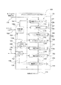
図9は、映像入力インタフェース102、命令実行器104、エッジ処理モジュール106、レベルアクティべーションモジュール108、画素生成モジュール110、画素合成モジュール112及び映像出力インタフェース114などの複数の内部モジュールから形成されるグラフィックオブジェクト用コプロセッサ100を示す。モジュール102〜114は、グラフィックオブジェクト用コプロセッサ100にオブジェクト記述入力118を処理させて、画素出力120を形成させる複数のプロセスから成るパイプライン116を形成する。パイプライン116は、図示されているように様々なモジュール102〜114をパイプライン状に互いに接続するパイプライン配線116a〜116fを含む。画素ベースオブジェクト成分などの取り出し又は変換を容易にするため、外部メモリバス124に結合するメモリインタフェースモジュール122や、JPEGデコーダ126などの別のモジュールも設けられている。
【0035】
パイプラインセグメント116a〜116fは様々なモジュール102〜114の間でレンダリングデータ及びメッセージを搬送し、これはグラフィックオブジェクト画像を高速レンダリングするために重要であるが、様々なモジュール102〜126を多くの集積システムアーキテクチャに共通する構成で互いに接続するために、コプロセッサ100内部には別のバス128も設けられている。
【0036】
映像入力インタフェース102は、図形オブジェクトを含めて、レンダリングすべき画像のページ記述言語(PDL)表現を受信するために、コプロセッサ100をオブジェクト記述入力118に結合し、そのようなデータをパイプライン116により操作できる形態又は順序に適宜編成するように動作する。好ましい構成におけるオブジェクト記述入力は、当該技術では知られているように、PCIバスを介して供給される。また、映像入力インタフェース102はパイプライン116では早い段階で使用されるべきでない指令データ、制御データ、命令データ及びオブジェクトデータと、直ちに使用されるべきデータとを分類し、他のデータをバス124を介してメモリインタフェース122に結合するローカルメモリに一時的に格納させる。
【0037】
命令実行器104は受信したPDLから命令を読み取って、処理し、それらの命令を、パイプライン116の他のモジュールにより解釈され且つ使用されるべく転送されるメッセージとしてフォーマッティングする。命令の機能と、その命令がパイプライン116に沿って処理(レンダリング)されるべきデータに付随することが必要であるか否かに応じて、バス128を介して送り出される命令もあれば、パイプラインセグメント116b〜116fを介して送り出される命令もあると考えられる。
【0038】
エッジ処理モジュール106はPDLで記述された図形オブジェクトから取り出されるエッジレコードを読み取り、ラスタ化表示全体にわたり、画素位置の順に、エッジごとに現在走査線との交差点を判定する。エッジレコードを走査線ごとの表示の順序に分類できるようにするため、これはいくつかの有効エッジリストを使用して実行されるのが好ましい。エッジ処理モジュール106はパイプライン配線116cに沿ってレベルアクティべーションモジュール108へ出力を供給する。レベルアクティべーションモジュール108は命令実行器104から、優先順位レベルに関連するメッセージと、現在走査線上の図形オブジェクトに関連する充填データとを受信する。それらのメッセージに含まれる情報は、図形オブジェクトの特性を表すレベルアクティべーションテーブルとして形成されるのが好ましい。エッジ処理モジュール106から受信されるエッジ交差データはそのテーブルに作用して、隣接するエッジの間に存在する画素列に対して有効状態であり且つレンダリングすべき画像に寄与するオブジェクトを判定させる。このようなプロセスは、不透明度の異なるオブジェクト並びにクリッピングオブジェクトを考慮に入れるのが好ましい。
【0039】
画素生成モジュール110は有効画素列を受信し、オブジェクトごとに画素の色を判定するか、又は有効エッジの間の画素位置ごとに使用すべき一連の色を判定する。この色には、不透明色、混合色又は対応する図形オブジェクトによりウィンドゥイングされる画素ベース画像が含まれるであろう。後者の場合、実際の画素データはバス128を介してメモリインタフェース122を通して取り出されても良い。画像が圧縮形態である場合、バス128へ取り出された圧縮データを画素生成モジュール110に供給する前に、JPEGデコーダ126により伸張することになる。その後、寄与オブジェクトごとの画素データは画素合成モジュール112へ送られ、そこで、現在画素位置における全ての有効オブジェクトに関わる画素値、又は現在走査線上の一連の画素位置における全ての有効オブジェクトの画素値を優先順位に従って互いに合成し、その位置又は一連の位置における画素値を求め、レンダリングする。映像出力インタフェース114は配線116fを介してレンダリングされた画素を受信し、バッファリングインタフェースの役割を実行して、画素出力120がそのようにしてレンダリングされた表示画像の走査線ごとに適切な画素値のラスタデータシーケンスとして確実に形成されるようにする。
【0040】
上記のように画素ベースの画像成分を取り出すために使用される他に、メモリインタフェース122は、パイプライン116に沿った様々な処理段階においてグラフィックス用コプロセッサ100の外部にあるメモリを利用させる。例えば、1つのパイプラインモジュールが、合成機能などの複雑で長い時間を要する処理に関わっている場合、先行する他のモジュールの動作が滞ってしまうことがある。そのような状況では、滞っていたプロセスが利用できるようになるときまでデータメッセージなどを外部メモリに一時格納しておいても良い。更に、好ましい実現形態においては、画素合成モジュール112はスタックマシンを使用して、式ツリーに基づく合成式を実行し、評価する。そのような式の大きさ(すなわち、寄与する有効オブジェクトの数)又はオブジェクトの複雑さ(例えば、画素画像)に応じて、外部メモリを使用してスタックを構築し、それを評価しても良い。
【0041】
コプロセッサ100内には、外部制御インタフェースモジュール130も設けられている。このモジュール130は、コプロセッサ100の動作のデバッギングを行う外部デバッグバス132に結合している。デバッグバス132は、様々なモジュール102〜126のそれぞれを図3から図5に示す機能性に対応する方式で外部制御インタフェースに結合するセグメント136a〜136jを有するデバッグループバス134に外部制御インタフェース130を介して結合している。従って、デバッグループバス134は、デバッグバス132を介するアクセスによって、モジュール102〜126のいずれかの動作のデバッギングを実行する。
【0042】
図9の構成でわかるように、デバッグループ134とそのセグメント136a〜136jは処理パイプライン116及びそれに対応する配線セグメント116a〜116fから隔離されており、また、主バス128からも隔離されている。そのため、モジュール102〜126のいずれかの動作のデバッギングは、画素出力120を提供するオブジェクト記述入力128のレンダリング処理を妨げることなく実行される。
【0043】
デバッグループバス134は映像入力インタフェース102内部のレジスタ及びメモリをアクセスする。このバス134は、テストパターンを書き込み、それらを再度読み取ることにより、メモリを試験するために使用される。レンダリング処理動作中、バス134を使用して映像入力インタフェース102における活動を監視することができる。そのような監視には、アドレスポインタ、ジョブサイズカウンタ及びデータアンパッキングカウンタの観測が含まれる。バス134では、入力118と関連するPCI構成設定を有するPCI構成レジスタも観測できるので、入力118の状態を監視できるであろう。更に、バス134は映像入力インタフェース102からの割り込みをイネーブルし、検査し、クリアすると共に、コプロセッサ100のソフトウェアリセットを生成するためのメカニズムも形成している。
【0044】
命令実行器104の内部にあり、デバッグループバス134を介してアクセス可能である状態レジスタは、メモリインタフェース122及びバス122に接続するローカルメモリから取り出すべき現在命令のアドレス及びデコードすべき現在命令を示す。バス134を使用して、命令実行器104内部の構成レジスタに書き込みを実行することにより、レンダリングジョブを送信し、打ち切ることも可能である。
【0045】
エッジ処理モジュール内部の状態レジスタはデバッグループバス134を介してアクセス可能であり、メモリインタフェース122を介してローカルメモリから現時点で取り出すべきエッジのアドレスを示す。
【0046】
レベルアクティべーションモジュール108内部の状態レジスタは、レベルアクティべーションモジュール108により処理すべき現在x座標及び現在動作を示す。レベルアクティべーションモジュール108からの有効オブジェクトデータをバッファリングするために設けられた出力充填キャッシュも、レベルアクティべーションモジュール108に含まれる構成レジスタを使用してオフできる。先に説明したレベルアクティべーションテーブルなどの、レベルアクティべーションモジュール108内部の全てのメモリは、読み取り動作及び書き込み動作を使用して、デバッグループバス134を介して問い合わせのためにも利用可能である。レベルアクティべーションモジュール108が不適当な優先順位レベルを検出するか、又は走査線の終端でも有効状態であることを検出すると、それらはデバッグループバス134を使用してアクセス可能である状態レジスタでも示される。
【0047】
画素生成モジュール110内部の状態レジスタは、現在キャッシュ制御信号と合成バス出力とを含み、デバッグループバス134を使用する検査のために利用可能である。画素生成モジュール110内部の充填テーブルも、読み取り及び書き込みの動作のために、デバッグループバス134において利用可能である。
【0048】
画素合成モジュール112内部の、デバッグループバス134を介してアクセス可能である状態レジスタは、使用すべき特定の合成モード(RGBO又はCMYK)、属性モード並びに現在合成色及び対応するパイプライン制御信号を識別するレジスタを含む。合成スタックを評価するために使用される、非事前乗算部検索テーブル(un-premultiply division look-up table)もデバッグループバス134において読み取り可能である。合成スタックのオーバフロー又はアンダフローの場合、そのことは専用の状態レジスタで指示される。
【0049】
映像出力インタフェース114のレジスタは、出力データフォーマット及び転送プロトコルの構成を行う。画素出力120を供給する出力ピンがデバッグループバス134に出力データを示すべく設定されるように、コプロセッサ100を構成しても良い。
【0050】
映像出力インタフェース114の状態レジスタは、現在x座標、走査線の長さ、メモリダンプバッファ(使用している場合)の場所と大きさなどの所望の情報を指示するために使用される。尚、メモリダンプバッファは、レンダリングされた画像を直ちに表示するのではなく、格納しておくべき場合に使用される。不当な命令が検出されたならば、これも同様にデバッグループバス134を使用してアクセス可能である映像出力インタフェース114の内部のレジスタで指示することができる。
【0051】
JPEGデコーダ126の状態レジスタは、デコーダが伸張タスクを有効的に実行しているか否かを示し、実行していれば、処理すべきカラーチャネルの数、動作の種類、変換の種類、タスクのリストの状態及びそのようなモジュールで使用される入力データFIFOレジスタの状態などの現在タスクのパラメータに対しアクセスを実行する。また、データの監視を可能にするために、現在タスクアドレス、現在データ取り出しアドレス、現在データ書き込みアドレス及びデータ出力などの低レベルデバッグ支援情報がJPEGデコーダ126内部に配列された様々なパイプライン化サブモジュールから提供される。JPEGデコーダ126内部に形成された全てのメモリも、読み取り及び書き込みの動作のために、デバッグループバス134で利用可能である。
【0052】
メモリインタフェース122は、デバッギングのために有用であると共に、製造試験にも使用される状態レジスタを含む。デバッギングのために有用であるレジスタは、バーストメモリ転送のための関連するburst_size、read_address_valid及びread_address_takenと共に、アクセスすべき特定の読み取りアドレスを格納している。後の2つのレジスタは、読み取り要求のパターンと、停止パターンを表すことができる要求/許可信号の可視性とを示すのに有用である。同様に、書き込み要求状態も利用可能である。モジュール102〜126のうち現在モジュール及び先行モジュールがメモリインタフェース122を介してローカルメモリへのアクセスを許可されたことに関する詳細は、モジュールの互いに対する要求パターンについての情報を更に提供する共通状態レジスタにおいても利用可能である。
【0053】
RAMbusコアなどのメモリインタフェース122の専用構成要素の製造試験のために要求されるいくつかの信号も状態レジスタとして利用可能である。デバッグループバス134は、それらのレジスタをごくわずかなコストで出力として見えるようにすることができる。
【0054】
外部制御インタフェース130は、マスタモードとスレーブモードの双方で動作することができる。コプロセッサ100のこの部分は複雑であるので、クロックドメイン境界の交差点 (a clock domain boundary crossing) に隣接するバスをデバッグモードで見ることができ、これによりデバッギングが簡単な作業になっている。更に、外部制御インタフェース130からコプロセッサ100に到達する制御信号も同時に見えるので、このような構成をとらないと発見することが不可能であるような故障を引き起こすおそれのあるプロトコル違反をデバッグループバス134を使用して観測することができる。
【0055】
デバッグモードでは、デバッグループバス134のマスタである外部制御インタフェース130は1回のクロックサイクルごとに全ての読み取りトランザクションを繰り返すため、絶え間なく監視を行うことができる。この繰り返し動作は、デバッグモードがオフされるか、又は異なるトランザクションが現れるまで続く。後者の場合、そのトランザクションが繰り返されるトランザクションになる。
【0056】
状態構成及び制御構成の更新を目的として構成された実施例に関連して本発明を説明したが、データへのアクセスが要求される用途であれば、多様な構成に本発明の適用を広げることができる。本発明のいくつかの実施例のみを説明したが、本発明の範囲から逸脱せずにそれらの実施例について変形を実施することは可能である。
【図面の簡単な説明】
【図1】 従来の構成を示す図。
【図2】 従来の別の構成を示す図。
【図3】 第1の実施例によるシーケンシャルバス構成を示す概略ブロック線図。
【図4】 図3のモジュール36の1つの内部における様々な接続を示す概略ブロック線図。
【図5】 図4に示すバスコントローラを示す概略ブロック線図。
【図6】 好ましい実施例のバスアーキテクチャにおける信号の順序を示すタイミング図。
【図7】 別の実施例を示す図。
【図8】 更に別の実施例を示す図。
【図9】 シーケンシャルバス構成を有する図形オブジェクトコプロセッサを示す概略ブロック線図。[0001]
Field of the Invention
The present invention relates to bus architectures, and more particularly to sequential configurations that consume minimal space when implemented in hardware, particularly integrated circuits.
[0002]
【background】
In the last few years, various bus architectures have been developed to handle various situations where it is required to communicate information between individual devices and / or modules in an electronic system. The extent to which a bus architecture can be used depends on several factors, including the data transfer rate to be realized by the bus, the specific environment in which the data transfer should be performed, the distance over which the data must be transferred, and so on.
[0003]
In a computing system such as a personal computer, the bus is usually formed by a plurality of parallel bidirectional configurations controlled by a microprocessor type device. In some situations, a single serial bus may be coupled to multiple devices or modules, but this allows individual modules to sense the interconnect utilization between modules and take advantage of data transmission. Rely on the operation of gaining control of the communication link at the moment. In such a configuration, there is one “speaker” on a certain line, but there are many “listeners”, so that data transmitted from one module can be reliably received by a desired destination module. In order to guarantee, it is necessary to realize a collision prevention configuration. The above-described configuration can be applied to both printed circuits and integrated circuits. However, when designing a circuit, various advantages and disadvantages are brought about depending on the particular implementation.
[0004]
A problem arises when this is applied to an integrated system that includes several modules that the integrated device desires to communicate with and that channels the communication through one external interface port associated with the integrated device. . Such a configuration is shown in FIG. As shown in FIG. 1, a single integrated
[0005]
One configuration for solving this problem is shown in FIG. In the
[0006]
It is an object of the present invention to substantially overcome or at least ameliorate one or more of the above problems and / or provide a bus architecture configuration that replaces conventional configurations.
[0007]
SUMMARY OF THE INVENTION
According to one aspect of the invention, there is an internal bus architecture of an integrated circuit device comprising a plurality of modules that are desired to perform communication via an access port of the integrated circuit device,
A plurality of bus segments, each connecting two of the modules to each other to form an interconnected closed loop of the two modules;
Each associated with a corresponding one of the modules and at least contributing to a unidirectional transfer of communication transactions from the access port to a destination module in the module along the closed loopA plurality of bus controllers corresponding to the number of bus segments;
In addition to the plurality of bus segments, the plurality of wiring segments that connect the plurality of modules to form a processing pipeline,
The plurality of bus segments constitute a debugging loop different from the processing pipeline,
The plurality of modules are:
A video input interface for inputting a page description language;
An instruction execution unit that reads and executes instructions from the received page description language;
An edge processing module that reads an edge extracted from a graphic object described in a page description language and determines an intersection of the edge and the scanning line;
A level activation module that determines an object that contributes to an image to be rendered in a valid state for pixel columns that exist between edges;
A pixel generation module that receives an effective pixel row and determines the color of a pixel for each object;
A pixel synthesis module that synthesizes pixel values of valid objects according to priority order to obtain pixel values and renders;
A video output interface for receiving rendered pixels and forming pixel values for each scan lineAn architecture comprising a plurality of bus controllers corresponding to the number of bus segments is disclosed.
[0008]
Other aspects of the invention are also disclosed.
[0009]
[Detailed explanation]
FIG. 3 illustrates a bus architecture system according to one embodiment of the present invention. The bus architecture system is formed in an
[0010]
Although not shown in FIG. 3, those of ordinary skill in the art will appreciate that the
[0011]
In the configuration of FIG. 3, the communication signal received by the
[0012]
The particular embodiment of the present invention described herein sets and tests configuration and control registers allocated to individual modules of an application specific large scale integrated circuit (ASIC) developed as a computer graphics coprocessor. Was born out of the need to perform. In this regard, the purpose of the sequential bus in the preferred embodiment is to configure the ASIC before actually operating the ASIC, and to perform a test of the ASIC's operation for debugging purposes. Thus, the speed at which the sequential bus of the preferred embodiment operates is not critical, thus providing an implementation that is inferior in terms of communication speed instead of saving chip space. As can be seen from FIG. 3, the sequential bus forms a daisy chain that connects the
[0013]
In the preferred embodiment, it is a
[0014]
The
(i) latching incoming transactions, so that a delay of one pipeline per module 36 is introduced; and
(ii) It is convenient to process the transaction within one clock cycle.
[0015]
By operating in this way, the waiting time sequentially generated on the daisy chain bus is reduced to one clock cycle for each module 36. By ensuring that the latency for each module 36 is equal, the overall latency of the entire daisy chain bus can be configured to be within certain design limits, so that requests for data or communication of data Any request for inevitably occurs in a known time period consistent with the operating conditions of the system in which the
[0016]
In the preferred embodiment, the
[0017]
Referring now to FIG. 5, the configuration of the
[0018]
The address signal component and the control signal component of the
[0019]
If the address decoded by the
[0020]
In the preferred embodiment,
[0021]
[Table 1]
The combination of the confirmation control signal and the valid control signal determines whether the address / data signal is a request or response to a particular module 36. Table 2 below shows the values of those bits in both request and response situations.
[0023]
[Table 2]
Table 3 below shows a specific breakdown of the register address bus element.
[0025]
[Table 3]
In the preferred embodiment, the request transaction is always initiated by the
[0027]
As shown in FIG. 6, the first transaction includes a request (adreq) at the address found on the reg_ad_in signal line, accompanied by a valid reg_valid_in signal. This is interpreted as a read to one of the
[0028]
The output will be taken into account by the next module 36, where it is sent uninterrupted with a one cycle delay. In a preferred implementation, the bus rise time td_r is less than 2 nanoseconds.
[0029]
For the configuration described above, several other configurations for returning data from the daisy chain bus are possible. The simplest first method is to limit the bus to one request / response at a time. Although expensive for queries, such a method inherently can reliably identify responses. The second method is to count clock cycles in a series of pipelined requests. Since each
[0030]
When the bus architecture is realized by a large-scale integrated circuit or the like, the above configuration is extremely useful. In the preferred embodiment, the 38-bit bus constitutes a randomly accessible communication link between the individual modules in the LSI graphics coprocessor, and any specifics around the device to which external connections are made. It is important that there is no bottleneck of the conductor even at the location. Thereby, when designing the integrated circuit, the individual modules can be distributed over the entire surface of the chip, and the modules can be arranged in an optimal relationship with each other while ensuring communication with the external device in an optimal state.
[0031]
The above configuration may be modified. That is, at least a part of the decoding operation shown in FIG. 5 may be executed by the node communication module.
[0032]
FIG. 7 shows such an
[0033]
In FIG. 8,
[0034]
FIG. 9 is formed from a plurality of internal modules such as a
[0035]
Pipeline segments 116a-116f carry rendering data and messages between the various modules 102-114, which is important for high speed rendering of graphic object images, but the various modules 102-126 are integrated in many ways. Another
[0036]
[0037]
The
[0038]
The
[0039]
The
[0040]
In addition to being used to extract pixel-based image components as described above, the
[0041]
An external
[0042]
As can be seen in the configuration of FIG. 9, the
[0043]
The
[0044]
A status register internal to the
[0045]
A status register within the edge processing module is accessible via the
[0046]
A status register within the
[0047]
The status register within the
[0048]
A status register within the
[0049]
The registers of the
[0050]
The status register of the
[0051]
The status register of the
[0052]
The
[0053]
Some signals required for manufacturing testing of dedicated components of the
[0054]
The
[0055]
In the debug mode, the
[0056]
Although the present invention has been described with reference to embodiments configured for the purpose of updating state configurations and control configurations, the application of the present invention can be extended to various configurations for applications that require access to data. Can do. Although only some embodiments of the present invention have been described, modifications may be made to these embodiments without departing from the scope of the present invention.
[Brief description of the drawings]
FIG. 1 is a diagram showing a conventional configuration.
FIG. 2 is a diagram showing another conventional configuration.
FIG. 3 is a schematic block diagram showing a sequential bus configuration according to the first embodiment.
4 is a schematic block diagram illustrating various connections within one of the modules 36 of FIG.
FIG. 5 is a schematic block diagram showing the bus controller shown in FIG. 4;
FIG. 6 is a timing diagram illustrating the order of signals in the preferred embodiment bus architecture.
FIG. 7 is a diagram showing another embodiment.
FIG. 8 is a diagram showing still another embodiment.
FIG. 9 is a schematic block diagram illustrating a graphic object coprocessor having a sequential bus configuration.
Claims (21)
各々が前記モジュールのうち2つのモジュールを互いに接続して、前記2つのモジュールの互いに接続された閉ループを形成する複数のバスセグメントと、
各々が前記モジュールのうち対応する1つと関連し、前記閉ループに沿った、前記アクセスポートから前記モジュールの中の宛先モジュールに至る通信トランザクションの単方向転送に少なくとも寄与し且つ前記バスセグメントの数に対応する複数のバスコントローラと、
前記複数のバスセグメントとは別に前記複数のモジュールを接続して処理パイプラインを構成する複数の配線セグメントとを具備し、
前記複数のバスセグメントは、前記処理パイプラインとは別のデバッグ用ループを構成し、
前記複数のモジュールは、
ページ記述言語を入力する映像入力インターフェースと、
受信したページ記述言語から命令を読み取り実行する命令実行部と、
ページ記述言語で記述された図形オブジェクトから取り出されるエッジを読み取り、エッジと走査線の交点を判定するエッジ処理モジュールと、
エッジ間に存在する画素列に対して有効状態で、レンダリングすべき画像に寄与するオブジェクトを判定するレベルアクティベーションモジュールと、
有効画素列を受信しオブジェクトごとの画素の色を判定する画素生成モジュールと、
有効オブジェクトの画素値を優先順位に従って合成し画素値を求めレンダリングする画素合成モジュールと、
レンダリングされた画素を受信し、走査線ごとの画素値を形成する映像出力インターフェースと
を含むことを特徴とするアーキテクチャシステム。In an internal bus architecture system of an integrated circuit device comprising a plurality of modules that are desired to communicate via an access port of the integrated circuit device,
A plurality of bus segments, each connecting two of the modules to each other to form an interconnected closed loop of the two modules;
Each associated with a corresponding one of the modules, contributing at least a unidirectional transfer of communication transactions from the access port to a destination module in the module along the closed loop and corresponding to the number of bus segments With multiple bus controllers
In addition to the plurality of bus segments, the plurality of wiring segments that connect the plurality of modules to form a processing pipeline,
The plurality of bus segments constitute a debugging loop different from the processing pipeline ,
The plurality of modules are:
A video input interface for inputting a page description language;
An instruction execution unit that reads and executes instructions from the received page description language;
An edge processing module that reads an edge extracted from a graphic object described in a page description language and determines an intersection of the edge and the scanning line;
A level activation module that determines an object that contributes to an image to be rendered in a valid state for pixel columns that exist between edges;
A pixel generation module that receives an effective pixel row and determines the color of a pixel for each object;
A pixel synthesis module that synthesizes pixel values of valid objects according to priority order to obtain pixel values and renders;
A video output interface that receives rendered pixels and forms pixel values for each scan line;
An architecture system characterized by including:
(a) 前記外部ポートで、前記モジュールの1つと関連する宛先アドレスを含む通信トランザクションを形成する工程と、
(b) 前記モジュールの各々で、前記モジュールと関連するアドレスとの対応性があるか否かに関して前記宛先アドレスを検査し、前記トランザクションを前記モジュールの間を順次通過させる工程と、
(c) 対応性がないと判定された場合、前記トランザクションを前記モジュールのうち次のモジュールへ送り出す工程と、
(d) 対応性があると判定された場合、前記宛先アドレスで前記トランザクションと関連する動作を実行する工程と、
(e) 前記モジュールを接続する処理パイプラインの前記バスセグメントとは別のデバッグループのセグメントを用いて前記モジュールのデバッグを行う工程と
を有し、
前記複数のモジュールは、
ページ記述言語を入力する映像入力インターフェースと、
受信したページ記述言語から命令を読み取り実行する命令実行部と、
ページ記述言語で記述された図形オブジェクトから取り出されるエッジを読み取り、エッジと走査線の交点を判定するエッジ処理モジュールと、
エッジ間に存在する画素列に対して有効状態で、レンダリングすべき画像に寄与するオブジェクトを判定するレベルアクティベーションモジュールと、
有効画素列を受信しオブジェクトごとの画素の色を判定する画素生成モジュールと、
有効オブジェクトの画素値を優先順位に従って合成し画素値を求めレンダリングする画素合成モジュールと、
レンダリングされた画素を受信し、走査線ごとの画素値を形成する映像出力インターフェースと
を含むことを特徴とする方法。In a method of performing communication between an external port of an integrated circuit device and one of a plurality of modules formed in the device,
(a) forming a communication transaction at the external port including a destination address associated with one of the modules;
(b) in each of the modules, checking the destination address for whether there is a correspondence with the address associated with the module, and sequentially passing the transactions between the modules;
(c) if it is determined that there is no correspondence, sending the transaction to the next module among the modules;
(d) if it is determined to be compatible, performing an operation associated with the transaction at the destination address;
(e) and the bus segment of the processing pipeline connecting the module possess and performing debugging of the module using a segment of another debug loop,
The plurality of modules are:
A video input interface for inputting a page description language;
An instruction execution unit that reads and executes instructions from the received page description language;
An edge processing module that reads an edge extracted from a graphic object described in a page description language and determines an intersection of the edge and the scanning line;
A level activation module that determines an object that contributes to an image to be rendered in a valid state for pixel columns that exist between edges;
A pixel generation module that receives an effective pixel row and determines the color of a pixel for each object;
A pixel synthesis module that synthesizes pixel values of valid objects according to priority order to obtain pixel values and renders;
A video output interface that receives rendered pixels and forms pixel values for each scan line;
A method comprising the steps of:
各々が前記モジュールのうち2つのモジュールを互いに接続して、前記2つのモジュールの互いに接続された閉ループを形成する複数のバスセグメントと、A plurality of bus segments, each connecting two of the modules to each other to form an interconnected closed loop of the two modules;
各々が前記モジュールのうち対応する1つと関連し、前記閉ループに沿った、前記アクセスポートから前記モジュールの中の宛先モジュールに至る通信トランザクションの単方向転送に少なくとも寄与し且つ前記バスセグメントの数に対応する複数のバスコントローラと、Each associated with a corresponding one of the modules, contributing at least a unidirectional transfer of communication transactions from the access port to a destination module in the module along the closed loop and corresponding to the number of bus segments With multiple bus controllers
前記複数のバスセグメントとは別に前記複数のモジュールを接続して処理パイプラインを構成する複数の配線セグメントとを具備し、In addition to the plurality of bus segments, the plurality of wiring segments that connect the plurality of modules to form a processing pipeline,
前記複数のモジュールは、The plurality of modules are:
ページ記述言語を入力する映像入力インターフェースと、A video input interface for inputting a page description language;
受信したページ記述言語から命令を読み取り実行する命令実行部と、An instruction execution unit that reads and executes instructions from the received page description language;
ページ記述言語で記述された図形オブジェクトから取り出されるエッジを読み取り、エッジと走査線の交点を判定するエッジ処理モジュールと、An edge processing module that reads an edge extracted from a graphic object described in a page description language and determines an intersection of the edge and the scanning line;
エッジ間に存在する画素列に対して有効状態で、レンダリングすべき画像に寄与するオブジェクトを判定するレベルアクティベーションモジュールと、A level activation module that determines an object that contributes to an image to be rendered in a valid state for pixel columns that exist between edges;
有効画素列を受信しオブジェクトごとの画素の色を判定する画素生成モジュール、A pixel generation module that receives an effective pixel row and determines the color of a pixel for each object;
有効オブジェクトの画素値を優先順位に従って合成し画素値を求めレンダリングする画素合成モジュールと、A pixel synthesis module that synthesizes pixel values of valid objects according to priority order to obtain pixel values and renders;
レンダリングされた画素を受信し、走査線ごとの画素値を形成する映像出力インターフェースとA video output interface that receives rendered pixels and forms pixel values for each scan line;
を含むことを特徴とするグラフィクスプロセッサ。A graphics processor comprising:
Applications Claiming Priority (3)
| Application Number | Priority Date | Filing Date | Title |
|---|---|---|---|
| AU0050 | 1993-07-20 | ||
| AUPQ0050A AUPQ005099A0 (en) | 1999-04-29 | 1999-04-29 | Sequential bus architecture |
| AUPQ0050 | 1999-04-29 |
Publications (3)
| Publication Number | Publication Date |
|---|---|
| JP2001005776A JP2001005776A (en) | 2001-01-12 |
| JP2001005776A5 JP2001005776A5 (en) | 2007-06-14 |
| JP4761487B2 true JP4761487B2 (en) | 2011-08-31 |
Family
ID=3814250
Family Applications (1)
| Application Number | Title | Priority Date | Filing Date |
|---|---|---|---|
| JP2000131103A Expired - Fee Related JP4761487B2 (en) | 1999-04-29 | 2000-04-28 | Bus architecture and information processing apparatus using the same |
Country Status (5)
| Country | Link |
|---|---|
| US (1) | US6662256B1 (en) |
| EP (1) | EP1049021B1 (en) |
| JP (1) | JP4761487B2 (en) |
| AU (1) | AUPQ005099A0 (en) |
| DE (1) | DE60041300D1 (en) |
Families Citing this family (18)
| Publication number | Priority date | Publication date | Assignee | Title |
|---|---|---|---|---|
| US6934785B2 (en) * | 2000-12-22 | 2005-08-23 | Micron Technology, Inc. | High speed interface with looped bus |
| US7032134B2 (en) * | 2001-03-28 | 2006-04-18 | Intel Corporation | Microprocessor design support for computer system and platform validation |
| US20030172190A1 (en) * | 2001-07-02 | 2003-09-11 | Globespanvirata Incorporated | Communications system using rings architecture |
| US20030196076A1 (en) * | 2001-07-02 | 2003-10-16 | Globespan Virata Incorporated | Communications system using rings architecture |
| JP4838458B2 (en) * | 2001-09-13 | 2011-12-14 | 富士通セミコンダクター株式会社 | Semiconductor device |
| KR100477641B1 (en) * | 2002-01-15 | 2005-03-23 | 삼성전자주식회사 | Bus system and path decision method therefor |
| US7113488B2 (en) * | 2002-04-24 | 2006-09-26 | International Business Machines Corporation | Reconfigurable circular bus |
| US7360007B2 (en) * | 2002-08-30 | 2008-04-15 | Intel Corporation | System including a segmentable, shared bus |
| US20070027485A1 (en) * | 2005-07-29 | 2007-02-01 | Kallmyer Todd A | Implantable medical device bus system and method |
| TWI446356B (en) | 2005-09-30 | 2014-07-21 | Mosaid Technologies Inc | Memory with output control and system thereof |
| US20070076502A1 (en) * | 2005-09-30 | 2007-04-05 | Pyeon Hong B | Daisy chain cascading devices |
| US7652922B2 (en) | 2005-09-30 | 2010-01-26 | Mosaid Technologies Incorporated | Multiple independent serial link memory |
| US20080263248A1 (en) * | 2007-04-20 | 2008-10-23 | Harriman David J | Multi-drop extension for a communication protocol |
| US9035957B1 (en) * | 2007-08-15 | 2015-05-19 | Nvidia Corporation | Pipeline debug statistics system and method |
| DE102010003521A1 (en) * | 2010-03-31 | 2011-10-06 | Robert Bosch Gmbh | Modular structure for data processing |
| EP2372490A1 (en) * | 2010-03-31 | 2011-10-05 | Robert Bosch GmbH | Circuit arrangement for a data processing system and method for data processing |
| US11127110B2 (en) * | 2017-03-01 | 2021-09-21 | Arm Limited | Data processing systems |
| CN111522757B (en) * | 2020-04-23 | 2023-08-22 | 上海琪云工业科技有限公司 | Interrupt reading and clearing control method based on I2C bus |
Family Cites Families (16)
| Publication number | Priority date | Publication date | Assignee | Title |
|---|---|---|---|---|
| US4378589A (en) * | 1976-12-27 | 1983-03-29 | International Business Machines Corporation | Undirectional looped bus microcomputer architecture |
| US4263736A (en) * | 1978-10-11 | 1981-04-28 | Colorado Time Systems, Inc. | Modular display system |
| US4356404A (en) * | 1981-05-26 | 1982-10-26 | Gte Automatic Electric Labs Inc. | Circuit for equipping a variable number of bus units on a closed loop bus |
| US4641308A (en) * | 1984-01-03 | 1987-02-03 | Texas Instruments Incorporated | Method of internal self-test of microprocessor using microcode |
| US4816993A (en) * | 1984-12-24 | 1989-03-28 | Hitachi, Ltd. | Parallel processing computer including interconnected operation units |
| DE3603751A1 (en) * | 1986-02-06 | 1987-08-13 | Siemens Ag | INFORMATION TRANSFER SYSTEM FOR THE TRANSFER OF BINARY INFORMATION |
| FR2605768B1 (en) * | 1986-10-23 | 1989-05-05 | Bull Sa | BUS CONTROL DEVICE CONSISTING OF SEVERAL INSULATING SEGMENTS |
| US4916647A (en) * | 1987-06-26 | 1990-04-10 | Daisy Systems Corporation | Hardwired pipeline processor for logic simulation |
| JPH0646413B2 (en) * | 1987-08-10 | 1994-06-15 | 日本電気株式会社 | Data processing processor |
| US5119481A (en) * | 1987-12-22 | 1992-06-02 | Kendall Square Research Corporation | Register bus multiprocessor system with shift |
| JPH01274539A (en) * | 1988-04-27 | 1989-11-02 | Fujitsu Ltd | Ring network |
| US5347515A (en) * | 1992-03-27 | 1994-09-13 | Pittway Corporation | Method and apparatus for global polling having contention-based address identification |
| US5375097A (en) * | 1993-06-29 | 1994-12-20 | Reddy; Chitranjan N. | Segmented bus architecture for improving speed in integrated circuit memories |
| GB9510509D0 (en) * | 1995-05-24 | 1995-07-19 | Thomson Consumer Electronics | A digital data bus system including arbitration |
| JPH0991262A (en) * | 1995-09-20 | 1997-04-04 | Fuji Xerox Co Ltd | Multiprocessor system |
| JP3202648B2 (en) * | 1997-04-11 | 2001-08-27 | 甲府日本電気株式会社 | Data transfer device and data transfer system |
-
1999
- 1999-04-29 AU AUPQ0050A patent/AUPQ005099A0/en not_active Abandoned
-
2000
- 2000-04-21 US US09/553,856 patent/US6662256B1/en not_active Expired - Lifetime
- 2000-04-28 JP JP2000131103A patent/JP4761487B2/en not_active Expired - Fee Related
- 2000-04-28 EP EP00303602A patent/EP1049021B1/en not_active Expired - Lifetime
- 2000-04-28 DE DE60041300T patent/DE60041300D1/en not_active Expired - Lifetime
Also Published As
| Publication number | Publication date |
|---|---|
| DE60041300D1 (en) | 2009-02-26 |
| EP1049021B1 (en) | 2009-01-07 |
| EP1049021A3 (en) | 2004-01-21 |
| EP1049021A2 (en) | 2000-11-02 |
| JP2001005776A (en) | 2001-01-12 |
| US6662256B1 (en) | 2003-12-09 |
| AUPQ005099A0 (en) | 1999-05-20 |
Similar Documents
| Publication | Publication Date | Title |
|---|---|---|
| JP4761487B2 (en) | Bus architecture and information processing apparatus using the same | |
| KR100188990B1 (en) | Data transfer device and video game apparatus using the device | |
| US8730248B2 (en) | Multi-graphics processor system, graphics processor and data transfer method | |
| JP7104448B2 (en) | Acceleration control system, chip and robot based on binarization algorithm | |
| JP2011170868A (en) | Pipeline accelerator for improved computing architecture, and related system and method | |
| JPH10207732A (en) | Integrated circuit device and its communication method | |
| JP2002530744A (en) | Communication system and method with multi-level connection identification | |
| JPH077374B2 (en) | Interface circuit | |
| US6766386B2 (en) | Method and interface for improved efficiency in performing bus-to-bus read data transfers | |
| KR19990062457A (en) | Data transfer method of the dynamic ram embedded microprocessor and the dynamic ram embedded microprocessor | |
| US7660924B2 (en) | Semiconductor integrated circuit device which executes data transfer between a plurality of devices connected over network, and data transfer method | |
| US7054979B2 (en) | Method and apparatus for routing configuration accesses from a primary port to a plurality of secondary ports | |
| JPH06214945A (en) | Computer system and high-speed transfer method of information | |
| US7472212B2 (en) | Multi CPU system | |
| AU749664B2 (en) | Sequential bus architecture | |
| KR20050064568A (en) | On-chip serialized peripheral bus system and operating method thereof | |
| JP7265953B2 (en) | Communication control system and information processing equipment | |
| JPH05342172A (en) | Multiprocessor system | |
| US20020069311A1 (en) | Bus control device | |
| JP2820054B2 (en) | Bus interface device | |
| JP2638505B2 (en) | Bus interface device | |
| JPH11282888A (en) | Data communication method in system to be designed based on system specification description, combination method of interruption controller and synthesizing method of interface circuit | |
| JPH07334453A (en) | Memory access system | |
| JP3183311B2 (en) | Data transfer system | |
| JP3505551B2 (en) | Data transfer control device and data transfer control system |
Legal Events
| Date | Code | Title | Description |
|---|---|---|---|
| A521 | Request for written amendment filed |
Free format text: JAPANESE INTERMEDIATE CODE: A523 Effective date: 20070426 |
|
| A621 | Written request for application examination |
Free format text: JAPANESE INTERMEDIATE CODE: A621 Effective date: 20070426 |
|
| RD03 | Notification of appointment of power of attorney |
Free format text: JAPANESE INTERMEDIATE CODE: A7423 Effective date: 20070426 |
|
| RD04 | Notification of resignation of power of attorney |
Free format text: JAPANESE INTERMEDIATE CODE: A7424 Effective date: 20080814 |
|
| A977 | Report on retrieval |
Free format text: JAPANESE INTERMEDIATE CODE: A971007 Effective date: 20100225 |
|
| A131 | Notification of reasons for refusal |
Free format text: JAPANESE INTERMEDIATE CODE: A131 Effective date: 20100326 |
|
| A521 | Request for written amendment filed |
Free format text: JAPANESE INTERMEDIATE CODE: A523 Effective date: 20100525 |
|
| A131 | Notification of reasons for refusal |
Free format text: JAPANESE INTERMEDIATE CODE: A131 Effective date: 20101001 |
|
| A521 | Request for written amendment filed |
Free format text: JAPANESE INTERMEDIATE CODE: A523 Effective date: 20101129 |
|
| TRDD | Decision of grant or rejection written | ||
| A01 | Written decision to grant a patent or to grant a registration (utility model) |
Free format text: JAPANESE INTERMEDIATE CODE: A01 Effective date: 20110603 |
|
| A01 | Written decision to grant a patent or to grant a registration (utility model) |
Free format text: JAPANESE INTERMEDIATE CODE: A01 |
|
| A61 | First payment of annual fees (during grant procedure) |
Free format text: JAPANESE INTERMEDIATE CODE: A61 Effective date: 20110606 |
|
| FPAY | Renewal fee payment (event date is renewal date of database) |
Free format text: PAYMENT UNTIL: 20140617 Year of fee payment: 3 |
|
| R150 | Certificate of patent or registration of utility model |
Free format text: JAPANESE INTERMEDIATE CODE: R150 |
|
| LAPS | Cancellation because of no payment of annual fees |