JP4752772B2 - AC motor winding switching device and winding switching system thereof - Google Patents
AC motor winding switching device and winding switching system thereof Download PDFInfo
- Publication number
- JP4752772B2 JP4752772B2 JP2007012370A JP2007012370A JP4752772B2 JP 4752772 B2 JP4752772 B2 JP 4752772B2 JP 2007012370 A JP2007012370 A JP 2007012370A JP 2007012370 A JP2007012370 A JP 2007012370A JP 4752772 B2 JP4752772 B2 JP 4752772B2
- Authority
- JP
- Japan
- Prior art keywords
- winding
- turned
- semiconductor switch
- unit
- motor
- Prior art date
- Legal status (The legal status is an assumption and is not a legal conclusion. Google has not performed a legal analysis and makes no representation as to the accuracy of the status listed.)
- Expired - Fee Related
Links
Images


Description
本発明は、3相交流電動機の巻線を切替えることによって、速度制御範囲を拡大する3相交流電動機の巻線切替装置に関するものであり、車両駆動、工作機械主軸駆動、サーボ装置を含む産業分野を対象とするものである。 The present invention relates to a winding switching device for a three-phase AC motor that expands the speed control range by switching the windings of the three-phase AC motor, and includes industrial fields including vehicle drive, machine tool spindle drive, and servo device. It is intended for.
従来から、電動機の半導体を用いた巻線切替の考え方は存在している。従来の技術例として、三相の整流ダイオードブリッジからなる整流部と、整流部によって作られた直流を短絡または開放する半導体スイッチからなるスイッチ部と、スイッチ部のスイッチング動作によって発生するサージエネルギーを吸収するスナバ部からなる電子スイッチがある。(例えば、特許文献1参照)。また、これとは異なり、スイッチ部を交流側に設置して実現しているものもある(例えば、特許文献2参照)。
図4において、1はインバータ、2は交流電動機、12は巻線切替部である。交流電動機2の巻線は低速運転用巻線と高速運転用巻線があり、巻線の中間と終端にタップを出し、これを巻線切替部12に接続する。巻線切替部12のSW1およびSW2をオンまたはオフすることで、低速運転用巻線と高速運転用巻線の切替が可能になる。
図5において、1はインバータ、2は交流電動機、12は巻線切替部である。交流電動機2の巻線は低速運転用巻線と高速運転用巻線があり、巻線の中間と終端にタップを出し、インバータ1と交流電動機2の間に双方向半導体スイッチで構成された巻線切替部12を設ける。巻線切替部の双方向半導体スイッチは、インバータ1および交流電動機2の各相に接続される。高速運転用巻線に接続された3つの双方向半導体スイッチと低速運転用巻線に接続された3つの双方向半導体スイッチをオンまたはオフさせることで、低速運転用巻線と高速運転用巻線の切替が可能になる。
このように、従来の装置は、半導体スイッチを用いて交流電動機の巻線切替を実現するものである。
In FIG. 4, 1 is an inverter, 2 is an AC motor, and 12 is a winding switching unit. The AC motor 2 has a low-speed operation winding and a high-speed operation winding. Taps are provided at the middle and the end of the winding and connected to the winding switching unit 12. By switching on and off SW1 and SW2 of the winding switching unit 12, switching between the low-speed operation winding and the high-speed operation winding is possible.
In FIG. 5, 1 is an inverter, 2 is an AC motor, and 12 is a winding switching unit. The winding of the AC motor 2 includes a winding for low speed operation and a winding for high speed operation, taps are provided at the middle and the end of the winding, and a winding constituted by a bidirectional semiconductor switch between the
As described above, the conventional apparatus realizes the switching of the winding of the AC motor using the semiconductor switch.
従来の巻線切替装置は、巻線切替スイッチを半導体素子で構成しており、高速の切替が可能である。しかし、半導体スイッチの導通損失が問題になり、特に大容量化したときの損失による効率低下が問題であった。
本発明はこのような問題点に鑑みてなされたものであり、半導体スイッチと機械的スイッチを組み合わせることで、半導体スイッチの特長である高速の切替を実現しつつ、問題点である導通損失による効率低下を解決できる巻線切替装置と方法を提供することを目的とする。また巻線切替信号そのものはインバータ主回路に用いるIGBTの駆動に用いるゲート信号と同じ構成の信号生成手段を用いてゲートドライブ回路の統一化を図る。またインバータ装置に異常を検出した場合でも瞬時に永久磁石形同期電動機が拘束状態となることを防止し負荷機械に悪影響を及ぼさないようにすることを目的とする。
In the conventional winding switching device, the winding switching switch is formed of a semiconductor element, and high-speed switching is possible. However, the conduction loss of the semiconductor switch becomes a problem, and in particular, the efficiency reduction due to the loss when the capacity is increased.
The present invention has been made in view of such problems. By combining a semiconductor switch and a mechanical switch, high-speed switching, which is a feature of the semiconductor switch, is achieved, and efficiency due to conduction loss, which is a problem. An object of the present invention is to provide a winding switching device and method capable of solving the degradation. Further, the winding switching signal itself uses a signal generating means having the same configuration as the gate signal used for driving the IGBT used in the inverter main circuit, thereby unifying the gate drive circuit. It is another object of the present invention to prevent a permanent magnet synchronous motor from being in a restrained state instantaneously even when an abnormality is detected in an inverter device so as not to adversely affect a load machine.
上記問題を解決するため、本発明は、次のように構成したのである。
インバータで駆動する交流電動機の複数の巻線を切替える巻線切替部と、前記巻線切替部を制御する制御回路部とを備えた巻線切替装置であって、
前記巻線切替部は交流入力側の各相端子を前記交流電動機の各相の巻線切替端子に接続した3相整流部と、前記3相整流部の直流出力の両端に設けた半導体スイッチと、前記3相整流部の交流入力部を短絡するように設けられた機械的スイッチとを備え、
前記制御回路部は前記半導体スイッチを開閉するゲートドライブ回路と前記機械的スイッチを開閉する駆動信号生成部を備え、
前記ゲートドライブ回路は、巻線切替信号に用いるゲート信号をインバータ主回路駆動に用いるゲート信号と同じ信号生成手段を用いてゲート回路を統一化したものである。
また、請求項1において前記巻線切替部は前記3相整流部の直流出力側に接続したスナバ回路と、前記スナバ回路から前記半導体スイッチへ電流が逆流しない方向に設けたダイオードを含むものである。
また、請求項1において前記制御回路部(100)は、低速運転をする低速巻線から高速運転をする高速巻線に切り替える際は、前記半導体スイッチ(SSW1)をオンし、ある遅れの後に前記半導体スイッチ(SSW1)と同一の連結端子に設けた前記機械的スイッチ(MSW1)をオンし、その後前記半導体スイッチ(SSW1)をオフし、前記高速巻線から前記低速巻線に切り替える際は、前記機械的スイッチ(MSW1)をオフすると同時に前記半導体スイッチ(SSW2)をオンし、ある遅れの後に前記機械的スイッチ(MSW2)をオンし、その後前記半導体スイッチ(SSW2)をオフする信号を生成するものである。
また、請求項1において前記制御回路部(100)は、低速巻線から高速巻線に切り替える場合、オフしていた前記低速巻線側の前記半導体スイッチ(SSW2)をオンさせ、この時点では前記半導体スイッチ(SSW2)と前記機械的スイッチ(MSW2)が両方ともオンしている状態とし、その後機前記械的スイッチ(MSW2)をオフさせ、一旦前記半導体スイッチ(SSW2)だけで導通している状態とし、その後前記半導体スイッチ(SSW2)をオフさせると同時に前記半導体スイッチ(SSW1)をオンさせ、その後前記機械的スイッチ(MSW1)をオンし、その後前記半導体スイッチ(SSW1)をオフし、
高速巻線から低速巻線に切り替える場合、オフしていた前記高速巻線側の前記半導体スイッチ(SSW1)をオンさせ、この時点では前記半導体スイッチ(SSW1)と前記機械的スイッチ(MSW1)が両方ともオンしている状態とし、その後前記機械的スイッチ(MSW1)をオフさせ、一旦前記半導体スイッチ(SSW1)だけで導通している状態とし、その後前記半導体スイッチ(SSW1)をオフさせると同時に前記半導体スイッチ(SSW2)をオンさせ、その後前記機械的スイッチ(MSW2)をオンし、その後前記半導体スイッチ(SSW2)をオフするものである。
また、 交流電動機と、前記交流電動機を駆動するインバータと、前記交流電動機の複数の巻線を切替える巻線切替部と、
前記巻線切替部を制御する制御回路部とを備えた巻線切替システムであって、
前記巻線切替部は交流入力側の各相端子を前記交流電動機の各相の巻線切替端子に接続した3相整流部と、前記3相整流部の直流出力の両端に設けた半導体スイッチと、前記3相整流部の交流入力部を短絡するように設けられた機械的スイッチとを備え、
前記制御回路部は前記半導体スイッチを開閉するゲートドライブ回路と前記機械的スイッチを開閉する駆動信号生成部を備え、
前記ゲートドライブ回路は、巻線切替信号に用いるゲート信号をインバータ主回路駆動に用いるゲート信号と同じ信号生成手段を用いてゲート回路を統一化したものである。
In order to solve the above problem, the present invention is configured as follows.
A winding switching device including a winding switching unit that switches a plurality of windings of an AC motor driven by an inverter, and a control circuit unit that controls the winding switching unit,
The winding switching unit includes a three-phase rectification unit in which each phase terminal on the AC input side is connected to a winding switching terminal of each phase of the AC motor, and a semiconductor switch provided at both ends of the DC output of the three-phase rectification unit, A mechanical switch provided to short-circuit the AC input unit of the three-phase rectification unit,
The control circuit unit includes a gate drive circuit that opens and closes the semiconductor switch and a drive signal generation unit that opens and closes the mechanical switch ,
In the gate drive circuit, the gate circuit is unified by using the same signal generation means as the gate signal used for driving the inverter main circuit.
The winding switching unit according to
Also, in
Further, in
When switching from a high-speed winding to a low-speed winding, the semiconductor switch (SSW1) on the high-speed winding side that has been turned off is turned on, and at this point both the semiconductor switch (SSW1) and the mechanical switch (MSW1) Both are turned on, then the mechanical switch (MSW1) is turned off, and only the semiconductor switch (SSW1) is in a conductive state, and then the semiconductor switch (SSW1) is turned off and at the same time the semiconductor The switch (SSW2) is turned on, then the mechanical switch (MSW2) is turned on, and then the semiconductor switch (SSW2) is turned off.
An AC motor; an inverter that drives the AC motor; a winding switching unit that switches a plurality of windings of the AC motor;
A winding switching system comprising a control circuit unit for controlling the winding switching unit,
The winding switching unit includes a three-phase rectification unit in which each phase terminal on the AC input side is connected to a winding switching terminal of each phase of the AC motor, and a semiconductor switch provided at both ends of the DC output of the three-phase rectification unit, A mechanical switch provided to short-circuit the AC input unit of the three-phase rectification unit,
The control circuit unit includes a gate drive circuit that opens and closes the semiconductor switch and a drive signal generation unit that opens and closes the mechanical switch ,
In the gate drive circuit, the gate circuit is unified by using the same signal generation means as the gate signal used for driving the inverter main circuit.
本発明によると、高速運転用巻線と低速運転用巻線を有する交流電動機の巻線切替を、その速度に応じてインバータ内部で設定することができるとともに、切替信号そのものはインバータ主回路に用いるIGBTの駆動に用いるゲート信号と同じ構成の信号生成手段を用いることができ、回路の統一化を図ることができる。
また、半導体スイッチと機械的スイッチを組み合わせることで、半導体スイッチの特長である高速の切替を実現しつつ、問題点である導通損失による効率低下を解決できる巻線切替装置を具備した交流電動機の巻線切替装置及びその巻線切替システムを実現できる。
According to the present invention, the switching of the AC motor having the high-speed operation winding and the low-speed operation winding can be set inside the inverter according to the speed, and the switching signal itself is used for the inverter main circuit. Signal generating means having the same configuration as the gate signal used for driving the IGBT can be used, and the circuit can be unified.
In addition, by combining a semiconductor switch and a mechanical switch, the winding of an AC motor equipped with a winding switching device that can solve the problem of reduced efficiency due to conduction loss while realizing high-speed switching, which is a feature of the semiconductor switch . A line switching device and its winding switching system can be realized.
以下、本発明の実施の形態について図を参照して説明する。 Hereinafter, embodiments of the present invention will be described with reference to the drawings.
図1は、本発明のインバータ装置で低速運転用巻線と高速運転用巻線を有する交流電動機を駆動する際の構成図である。図において1はインバータ部、2は交流電動機、12は巻線切替部である。Pはインバータ部1の正側入力端子、Nは負側入力端子であり、PN間には直流電源が接続される。交流電動機2の巻線は低速運転用巻線と高速運転用巻線がある。巻線の中間(TU2、TV2、TW2)と両端に端子(TU1、TV1、TW1、TU3、TV3、TW3)を出し、中間端子(TU2、TV2、TW2)と交流電動機の巻線の一端(TU3、TV3、TW3)を巻線切替部12のそれぞれの三相整流部(3、4)の交流側へ接続する。端子U1−U3,V1−V3,W1−W3間の巻線全てを使う場合が低速運転用巻線となる。一方、端子U1−U2,V1−V2,W1−W2間の巻線だけを使う場合が高速運転用巻線となる。永久磁石形同期電動機の誘起電圧は速度に比例して大きくなるため、高速運転するためには誘起電圧を小さくする必要があるためである。低速運転用巻線の場合は中間端子(TU2、TV2、TW2)を全て開放すると共に端子(TU3、TV3、TW3)を全て接続しY結線を構成する。他方、高速運転用巻線の場合は端子(TU3、TV3、TW3)を全て開放すると共に中間端子(TU2、TV2、TW2)を全て接続しY結線を構成する。
FIG. 1 is a configuration diagram when an AC motor having a low-speed operation winding and a high-speed operation winding is driven by the inverter device of the present invention. In the figure, 1 is an inverter unit, 2 is an AC motor, and 12 is a winding switching unit. P is a positive input terminal of the
インバータ部1および巻線切替部12を駆動するための制御回路部100は、CPU110、巻線切替信号生成部111、PWM信号生成部112、ゲートドライブ回路113、機械的スイッチMSW1、MSW2の駆動信号を生成する駆動信号生成部114から構成される。機械的スイッチMSW1、MSW2は例えば、3相各相を同時に開閉する電磁接触器である。接触端子部の劣化を防止し信頼性を向上させた電磁接触端子部をガスで密封したものを使うこともできる。機械的スイッチ(MSW1、MSW2)の構成はインバータ部の筐体に内蔵させ、巻線切替装置全体をより小形に構成できる。
またゲートドライブ回路113はインバータ部1の主回路スイッチング素子であるIGBTと巻線切替部12の半導体スイッチSSW1およびSSW2の駆動信号を生成し、主回路スイッチング素子と巻線切替部12の半導体スイッチSSW1およびSSW2のゲートへ出力する。また機械的スイッチMSW1、MSW2の駆動信号を生成する駆動信号生成部114は巻線切替部12の機械的スイッチMSW1およびMSW2の駆動信号を生成し、その駆動信号を機械的スイッチMSW1およびMSW2へ出力する。
なお、各種用途に応じてインバータ装置の上位制御装置の指令に従って、CPU100は巻線切替信号生成部111へ巻線切替信号を出力する。インバータ装置自身がアプリケーションプログラムソフトウェアを備えている場合は上位制御装置を持たずにインバータ装置が交流電動機の位置や速度情報を基にして巻線切替信号生成部111へ巻線切替信号を出力する。
The control circuit unit 100 for driving the
The
Note that the CPU 100 outputs a winding switching signal to the winding switching
本発明が従来技術と異なる部分は巻線切替部12において、半導体スイッチSSW1、SSW2だけでなく機械的スイッチMSW1、MSW2を巻線の中間端子(TU2、TV2、TW2)と巻線の一端(TU3、TV3、TW3)をそれぞれ直接短絡できるように三相整流部入力と並列接続した部分とこれら機械的スイッチMSW1、MSW2を駆動するためのMSW1、MSW2駆動信号生成部114を備えた部分である。
巻線切替部12は、三相整流部(3、4)、三相整流部出力端を開閉する半導体スイッチ(SSW1、SSW2)、スナバ回路(5、6)、スナバ回路(5、6)から半導体スイッチ(SSW1、SSW2)への逆流電流防止のためのダイオード(7〜10)、機械的スイッチ(MSW1、MSW2)から構成される。スナバ回路(5、6)は、抵抗とコンデンサとの並列回路で構成される。
The present invention is different from the prior art in a winding switching unit 12 in which not only the semiconductor switches SSW1 and SSW2 but also mechanical switches MSW1 and MSW2 are connected to intermediate terminals (TU2, TV2, TW2) of the winding and one end of the winding (TU3). , TV3, TW3) are connected in parallel with the input of the three-phase rectifier so that they can be directly short-circuited, and are provided with MSW1, MSW2
The winding switching unit 12 includes a three-phase rectification unit (3, 4), a semiconductor switch (SSW1, SSW2) that opens and closes the output terminal of the three-phase rectification unit, a snubber circuit (5, 6), and a snubber circuit (5, 6). It comprises a diode (7-10) for preventing a backflow current to the semiconductor switches (SSW1, SSW2) and mechanical switches (MSW1, MSW2). The snubber circuit (5, 6) is composed of a parallel circuit of a resistor and a capacitor.
また、図1は交流電動機の巻線が2分割された状態の場合を示しているが、分割数が増える場合は、それに対応した数の巻線切替部を増設することで対応でき、図1の2分割の構成に限定するものではない。また交流電動機は誘導電動機、永久磁石を用いた同期電動機(回転子鉄心内部に磁石を埋め込んだタイプ、回転子表面に磁石を配置したタイプ)どちらでも本発明は適用できる。 FIG. 1 shows a case where the winding of the AC motor is divided into two. However, when the number of divisions increases, it can be dealt with by adding a corresponding number of winding switching units. However, the present invention is not limited to the two-divided configuration. In addition, the present invention can be applied to either an induction motor or a synchronous motor using a permanent magnet (a type in which a magnet is embedded in a rotor core, or a type in which a magnet is arranged on a rotor surface).
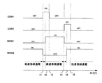
図2は本発明のインバータ装置における、巻線切替動作時のシーケンスを示す。一般に、半導体スイッチ(SSW1、SSW2)がゲート(ベース)信号を入力して数μsオーダで動作するのに対し、機械的スイッチでは数ms〜数百msの動作遅れが発生するため、まずオンするべき巻線に対応した半導体スイッチをオンし、ある遅れの後に機械的スイッチをオンする。図の例では、低速巻線から高速巻線に切り替える際、まず時刻t1で半導体スイッチSSW1をオンし、ある遅れの後に時刻t2でMSW1をオンする。機械的スイッチMSW1を時刻t2でオンした後、半導体スイッチSSW1を時刻t3でオフすることで、半導体スイッチSSW1で発生する導通損失をなくすことができる。
次に高速巻線から低速巻線に切り替える際、まずこれまで通電していた機械的スイッチMSW1を時刻t4でオフする。時刻t4で同時に半導体スイッチSSW2をオンし、ある遅れの後に機械的スイッチMSW2が時刻t5でオンする。機械的スイッチMSW2を時刻t5でオンした後、半導体スイッチSSW2を時刻t6でオフすることで半導体スイッチSSW2で発生する導通損失をなくすことができる。
FIG. 2 shows a sequence during the coil switching operation in the inverter device of the present invention. In general, the semiconductor switches (SSW1, SSW2) operate in the order of several μs by inputting gate (base) signals, whereas mechanical switches cause an operation delay of several ms to several hundred ms. The semiconductor switch corresponding to the power winding is turned on, and the mechanical switch is turned on after a certain delay. In the example shown in the figure, when switching from the low-speed winding to the high-speed winding, first, the semiconductor switch SSW1 is turned on at time t1, and MSW1 is turned on at time t2 after a certain delay. After the mechanical switch MSW1 is turned on at time t2, the semiconductor switch SSW1 is turned off at time t3, so that conduction loss generated in the semiconductor switch SSW1 can be eliminated.
Next, when switching from the high-speed winding to the low-speed winding, first, the mechanical switch MSW1 that has been energized so far is turned off at time t4. At time t4, the semiconductor switch SSW2 is turned on at the same time, and after a certain delay, the mechanical switch MSW2 is turned on at time t5. After the mechanical switch MSW2 is turned on at time t5, the semiconductor switch SSW2 is turned off at time t6, so that the conduction loss generated in the semiconductor switch SSW2 can be eliminated.
図3は本発明のインバータ装置における、巻線切替動作時の別のシーケンスを示す。図2の動作が基本的な動作であるが、機械的スイッチMSW1およびMSW2をオフするときの動作遅れを考慮する場合、図3のシーケンスにすることで、機械的スイッチMSW1およびMSW2のオフ時の動作遅れの問題を解決できる。図の例では、低速巻線から高速巻線に切り替える際、オフしていた低速巻線側の半導体スイッチSSW2を時刻t1でオンさせ、この時点(時刻t1)では半導体スイッチSSW2と機械的スイッチMSW2が両方ともオンしている状態となる。ここで先に時刻t2で機械的スイッチMSW2をオフさせ、一旦半導体スイッチSSW2だけで導通している状態(区間[t2,t3])にする。この後、半導体スイッチSSW2を時刻t3でオフさせると同時に半導体スイッチSSW1をオンさせることで、半導体スイッチのみによる切り替えが可能になり、オフする際の機械的スイッチの動作遅れの問題を解決できる。その後時刻t4で機械的スイッチMSW1をオンし、その後時刻t5で半導体スイッチSSW1をオフする。 FIG. 3 shows another sequence during the winding switching operation in the inverter device of the present invention. The operation of FIG. 2 is a basic operation. However, when considering the operation delay when turning off the mechanical switches MSW1 and MSW2, the sequence shown in FIG. 3 is used to turn off the mechanical switches MSW1 and MSW2. Can solve the problem of operation delay. In the example of the figure, when switching from the low-speed winding to the high-speed winding, the semiconductor switch SSW2 on the low-speed winding side that was turned off is turned on at time t1, and at this time (time t1), the semiconductor switch SSW2 and the mechanical switch MSW2 Are both turned on. Here, the mechanical switch MSW2 is first turned off at the time t2, and the semiconductor switch SSW2 alone is once in a conductive state (section [t2, t3]). Thereafter, the semiconductor switch SSW2 is turned off at the time t3 and at the same time the semiconductor switch SSW1 is turned on, so that the switching can be performed only by the semiconductor switch, and the problem of the operation delay of the mechanical switch at the time of turning off can be solved. Thereafter, the mechanical switch MSW1 is turned on at time t4, and then the semiconductor switch SSW1 is turned off at time t5.
高速巻線から低速巻線に切り替える際にも、同様にして図3のように半導体スイッチのみで切り替える動作を行うことができる。すなわち、高速巻線から低速巻線に切り替える際、オフしていた高速巻線側の半導体スイッチSSW1を時刻t6でオンさせ、この時点(時刻t6)では半導体スイッチSSW1と機械的スイッチMSW1が両方ともオンしている状態となる。ここで先に時刻t7で機械的スイッチMSW1をオフさせ、一旦半導体スイッチSSW1だけで導通している状態(区間[t7,t8])にする。この後、半導体スイッチSSW1を時刻t8でオフさせると同時に半導体スイッチSSW2をオンさせることで、半導体スイッチのみによる切り替えが可能になり、オフする際の機械的スイッチの動作遅れの問題を解決できる。時刻t9で機械的スイッチMSW2をオンし、その後時刻t10で半導体スイッチSSW2をオフする。
このように、本発明では、巻線切替を必要とする交流電動機の駆動用のインバータ装置において、巻線切替部には半導体スイッチと機械的スイッチの両方を備えることで、半導体スイッチの高速切替動作と、機械的スイッチの低損失の両方の長所を併せ持つことができる。
Similarly, when switching from the high-speed winding to the low-speed winding, the switching operation can be performed only by the semiconductor switch as shown in FIG. That is, when switching from the high-speed winding to the low-speed winding, the semiconductor switch SSW1 on the high-speed winding side that was turned off is turned on at time t6, and at this time (time t6), both the semiconductor switch SSW1 and the mechanical switch MSW1 are It will be on. Here, at time t7, the mechanical switch MSW1 is first turned off, and the semiconductor switch SSW1 alone is once in a conductive state (section [t7, t8]). Thereafter, the semiconductor switch SSW1 is turned off at the time t8 and at the same time the semiconductor switch SSW2 is turned on, so that switching by only the semiconductor switch becomes possible, and the problem of the operation delay of the mechanical switch at the time of turning off can be solved. At time t9, the mechanical switch MSW2 is turned on, and then at time t10, the semiconductor switch SSW2 is turned off.
As described above, according to the present invention, in the inverter device for driving an AC motor that requires winding switching, the winding switching unit includes both the semiconductor switch and the mechanical switch, so that the high-speed switching operation of the semiconductor switch is performed. And the advantages of both low loss and mechanical switch.
また、本発明のインバータ装置において、巻線切替部を電動機の保護装置として動作させることができる。インバータ装置において発生する問題の多くは、主回路パワー半導体素子(IGBT)の故障であり、たとえば、ある相のIGBTの上下短絡が発生した場合、交流電動機2が永久磁石を内蔵する同期電動機であると、瞬時に電動機がロック状態になり、電動機が接続される機械側に悪影響を及ぼす。本インバータ装置では、一般的にインバータ装置で実用化されているIGBTの上下短絡防止機能が動作すると直ちに、CPU110を介して巻線切替部12中の半導体スイッチSSW1、SSW2、機械的スイッチMSW1、MSW2を全てオフ状態にすることで、電動機をフリーラン状態(回転子の慣性モーメントにより惰力で回転しているいわゆる惰走状態)にすることができ、電動機がロックすることなく安全に自然減速することができる。この保護機能は、IGBTの上下短絡時に限るものではなく、インバータ装置で何らかの異常が発生した場合に、CPU110を介して常に巻線切替部12における保護機能を有効にすることができる。たとえば、通常のインバータ装置であると、何らかの異常でインバータ部のIGBTがゲートブロック動作し、全ての素子が開放した瞬間、電動機巻線に蓄えられていたエネルギーは全てインバータ部に瞬時に回生され、インバータ部において直流母線電圧の急激上昇が発生する。本発明のインバータ装置のように、巻線切替部を備えるインバータ装置であると、異常の瞬間に巻線切替部を全てオフにして、電動機巻線を開放状態にすることができるので、上記の問題は発生しない。電動機をフリーラン状態にする場合のインバータ装置の異常としては、電動機の運転継続できないようなインバータ部1の主回路パワー半導体素子(IGBT)の上下短絡、地絡故障、商用電源の停電、その他インバータ装置で備えている各種保護動作が想定される。
In the inverter device of the present invention, the winding switching unit can be operated as a motor protection device. Many of the problems that occur in the inverter device are failures of the main circuit power semiconductor element (IGBT). For example, when a vertical short circuit of an IGBT of a certain phase occurs, the AC motor 2 is a synchronous motor in which a permanent magnet is incorporated. Then, the electric motor is instantly locked and adversely affects the machine side to which the electric motor is connected. In the present inverter device, as soon as the IGBT vertical short circuit prevention function generally put into practical use in the inverter device operates, the semiconductor switches SSW1 and SSW2 and mechanical switches MSW1 and MSW2 in the winding switching unit 12 are connected via the
本発明は、巻線切替を必要とする交流電動機を駆動するインバータ装置の、特に巻き線切替部に関するものである。これは、回転形の交流電動機に限定されるものではなく、リニアモータの巻線切替にも適用できる。 The present invention relates to an inverter device that drives an AC motor that requires winding switching, and more particularly to a winding switching unit. This is not limited to a rotary AC motor, and can also be applied to switching of a winding of a linear motor.
1 インバータ部
2 交流電動機
3、4 3相整流部
5、6 スナバ回路
7〜10 ダイオード
12 巻線切替部
100 制御回路部
110 CPU
111 巻線切替信号生成部
112 PWM信号生成部
113 ゲートドライブ回路
114 MSW1、MSW2駆動信号生成部
SSW1、SSW2 半導体スイッチ
MSW1、MSW2 機械的スイッチ
P インバータの正側入力端子
N インバータの負側入力端子
P1 スナバ回路の正側端子
N1 スナバ回路の負側端子
P2 スナバ回路の正側端子
N2 スナバ回路の負側端子
DESCRIPTION OF
111 Winding
SSW1, SSW2 Semiconductor switch MSW1, MSW2 Mechanical switch P Inverter positive input terminal N Inverter negative input terminal P1 Snubber circuit positive terminal N1 Snubber circuit negative terminal P2 Snubber circuit positive terminal N2 Snubber circuit positive terminal Negative terminal
Claims (5)
前記巻線切替部は交流入力側の各相端子を前記交流電動機の各相の巻線切替端子に接続した3相整流部と、前記3相整流部の直流出力の両端に設けた半導体スイッチと、前記3相整流部の交流入力部を短絡するように設けられた機械的スイッチとを備え、
前記制御回路部は前記半導体スイッチを開閉するゲートドライブ回路と前記機械的スイッチを開閉する駆動信号生成部を備え、
前記ゲートドライブ回路は、巻線切替信号に用いるゲート信号をインバータ主回路駆動に用いるゲート信号と同じ信号生成手段を用いてゲート回路を統一化したものである交流電動機の巻線切替装置。 A winding switching device including a winding switching unit that switches a plurality of windings of an AC motor driven by an inverter, and a control circuit unit that controls the winding switching unit,
The winding switching unit includes a three-phase rectification unit in which each phase terminal on the AC input side is connected to a winding switching terminal of each phase of the AC motor, and a semiconductor switch provided at both ends of the DC output of the three-phase rectification unit, A mechanical switch provided to short-circuit the AC input unit of the three-phase rectification unit,
The control circuit unit includes a gate drive circuit that opens and closes the semiconductor switch and a drive signal generation unit that opens and closes the mechanical switch ,
The gate drive circuit is a winding switching device for an AC motor in which the gate circuit is unified by using the same signal generating means as the gate signal used for driving the inverter main circuit .
高速巻線から低速巻線に切り替える場合、オフしていた前記高速巻線側の前記半導体スイッチ(SSW1)をオンさせ、この時点では前記半導体スイッチ(SSW1)と前記機械的スイッチ(MSW1)が両方ともオンしている状態とし、その後前記機械的スイッチ(MSW1)をオフさせ、一旦前記半導体スイッチ(SSW1)だけで導通している状態とし、その後前記半導体スイッチ(SSW1)をオフさせると同時に前記半導体スイッチ(SSW2)をオンさせ、その後前記機械的スイッチ(MSW2)をオンし、その後前記半導体スイッチ(SSW2)をオフする請求項1記載の交流電動機の巻線切替装置。 When switching from the low-speed winding to the high-speed winding, the control circuit unit (100) turns on the semiconductor switch (SSW2) on the low-speed winding side that has been turned off. Both the mechanical switches (MSW2) are turned on, then the mechanical switches (MSW2) are turned off, and only the semiconductor switch (SSW2) is turned on, and then the semiconductor switches (SSW2) is turned off and at the same time the semiconductor switch (SSW1) is turned on, then the mechanical switch (MSW1) is turned on, and then the semiconductor switch (SSW1) is turned off,
When switching from a high-speed winding to a low-speed winding, the semiconductor switch (SSW1) on the high-speed winding side that has been turned off is turned on, and at this point both the semiconductor switch (SSW1) and the mechanical switch (MSW1) Both are turned on, then the mechanical switch (MSW1) is turned off, and only the semiconductor switch (SSW1) is in a conductive state, and then the semiconductor switch (SSW1) is turned off and at the same time the semiconductor The winding switching device for an AC motor according to claim 1, wherein the switch (SSW2) is turned on, the mechanical switch (MSW2) is turned on, and then the semiconductor switch (SSW2) is turned off.
前記巻線切替部を制御する制御回路部とを備えた巻線切替システムであって、
前記巻線切替部は交流入力側の各相端子を前記交流電動機の各相の巻線切替端子に接続した3相整流部と、前記3相整流部の直流出力の両端に設けた半導体スイッチと、前記3相整流部の交流入力部を短絡するように設けられた機械的スイッチとを備え、
前記制御回路部は前記半導体スイッチを開閉するゲートドライブ回路と前記機械的スイッチを開閉する駆動信号生成部を備え、
前記ゲートドライブ回路は、巻線切替信号に用いるゲート信号をインバータ主回路駆動に用いるゲート信号と同じ信号生成手段を用いてゲート回路を統一化したものである交流電動機の巻線切替システム。 An AC motor, an inverter that drives the AC motor, a winding switching unit that switches a plurality of windings of the AC motor,
A winding switching system comprising a control circuit unit for controlling the winding switching unit,
The winding switching unit includes a three-phase rectification unit in which each phase terminal on the AC input side is connected to a winding switching terminal of each phase of the AC motor, and a semiconductor switch provided at both ends of the DC output of the three-phase rectification unit, A mechanical switch provided to short-circuit the AC input unit of the three-phase rectification unit,
The control circuit unit includes a gate drive circuit that opens and closes the semiconductor switch and a drive signal generation unit that opens and closes the mechanical switch ,
The gate drive circuit is a winding switching system for an AC motor in which the gate circuit is unified by using the same signal generating means as the gate signal used for driving the inverter main circuit.
Priority Applications (1)
| Application Number | Priority Date | Filing Date | Title |
|---|---|---|---|
| JP2007012370A JP4752772B2 (en) | 2007-01-23 | 2007-01-23 | AC motor winding switching device and winding switching system thereof |
Applications Claiming Priority (1)
| Application Number | Priority Date | Filing Date | Title |
|---|---|---|---|
| JP2007012370A JP4752772B2 (en) | 2007-01-23 | 2007-01-23 | AC motor winding switching device and winding switching system thereof |
Publications (3)
| Publication Number | Publication Date |
|---|---|
| JP2008182783A JP2008182783A (en) | 2008-08-07 |
| JP2008182783A5 JP2008182783A5 (en) | 2011-03-10 |
| JP4752772B2 true JP4752772B2 (en) | 2011-08-17 |
Family
ID=39726257
Family Applications (1)
| Application Number | Title | Priority Date | Filing Date |
|---|---|---|---|
| JP2007012370A Expired - Fee Related JP4752772B2 (en) | 2007-01-23 | 2007-01-23 | AC motor winding switching device and winding switching system thereof |
Country Status (1)
| Country | Link |
|---|---|
| JP (1) | JP4752772B2 (en) |
Families Citing this family (15)
| Publication number | Priority date | Publication date | Assignee | Title |
|---|---|---|---|---|
| JP4906836B2 (en) * | 2008-04-07 | 2012-03-28 | 三菱電機株式会社 | Electric motor drive device, refrigeration air conditioner, and electric motor drive method |
| JP5396920B2 (en) * | 2009-03-05 | 2014-01-22 | 株式会社安川電機 | Winding switching device for three-phase AC motor drive system |
| JP5585783B2 (en) * | 2011-04-14 | 2014-09-10 | 株式会社安川電機 | AC motor winding switching device and AC motor drive system |
| JP2013099068A (en) * | 2011-10-31 | 2013-05-20 | Juki Corp | Controller of stepping motor |
| JP6009834B2 (en) * | 2012-06-22 | 2016-10-19 | 株式会社東芝 | Driving device and motor winding switching method |
| KR102182790B1 (en) * | 2012-11-14 | 2020-11-26 | 큐엠 파워, 인크. | Divided phase ac synchronous motor controller |
| CN103281034B (en) * | 2013-05-03 | 2015-05-13 | 哈尔滨工业大学 | Multi-phase motor winding switching circuit |
| JP6630561B2 (en) | 2015-12-15 | 2020-01-15 | 三菱重工業株式会社 | Motor drive control device provided with motor winding changeover switch, motor, compressor, and motor winding changeover control method |
| JP6614578B2 (en) | 2016-03-28 | 2019-12-04 | 三菱重工業株式会社 | Motor control device and compressor |
| CN109804552B (en) * | 2016-10-13 | 2022-08-30 | 三菱电机株式会社 | Motor drive device, motor system, and refrigeration cycle device |
| KR20180060017A (en) * | 2016-11-28 | 2018-06-07 | 서울과학기술대학교 산학협력단 | Multi- stage transmission system and method for controlling thereof |
| WO2020021681A1 (en) * | 2018-07-26 | 2020-01-30 | 三菱電機株式会社 | Electric motor drive device and refrigeration-cycle application device |
| WO2020179008A1 (en) * | 2019-03-06 | 2020-09-10 | 三菱電機株式会社 | Electric motor driving device and air conditioner |
| JP7262262B2 (en) * | 2019-03-25 | 2023-04-21 | 株式会社日立製作所 | Winding switching device for rotating electrical machine, rotating electrical machine drive system, and electric equipment |
| CN113572390A (en) * | 2021-05-07 | 2021-10-29 | 联合汽车电子有限公司 | Driving method for noise suppression of brushless direct current motor |
Family Cites Families (2)
| Publication number | Priority date | Publication date | Assignee | Title |
|---|---|---|---|---|
| JP3759334B2 (en) * | 1999-06-02 | 2006-03-22 | 富士電機デバイステクノロジー株式会社 | DC-AC power conversion circuit |
| JP3948009B2 (en) * | 2001-10-03 | 2007-07-25 | 株式会社安川電機 | Winding switching device for three-phase AC motor |
-
2007
- 2007-01-23 JP JP2007012370A patent/JP4752772B2/en not_active Expired - Fee Related
Also Published As
| Publication number | Publication date |
|---|---|
| JP2008182783A (en) | 2008-08-07 |
Similar Documents
| Publication | Publication Date | Title |
|---|---|---|
| JP4752772B2 (en) | AC motor winding switching device and winding switching system thereof | |
| JP4662316B2 (en) | AC motor winding switching device and winding switching system thereof | |
| JP6169203B1 (en) | Electric motor control apparatus and electric motor control method | |
| JP5398815B2 (en) | Permanent magnet synchronous motor driving device, air conditioner, ventilation fan driving device, washing machine, automobile and vehicle | |
| JP5325483B2 (en) | Motor drive device | |
| JP6636207B2 (en) | Motor drive unit and refrigeration cycle application equipment | |
| KR102066364B1 (en) | Power converter and electric power steering | |
| JP5077348B2 (en) | Motor drive device, motor device, and integrated circuit device | |
| JP2009303298A (en) | Ac motor device | |
| JP2012010568A (en) | Vehicle control system | |
| JP2017175747A (en) | Power conversion device | |
| JP5396920B2 (en) | Winding switching device for three-phase AC motor drive system | |
| JP2017011820A (en) | Motor drive device | |
| JP5003173B2 (en) | AC motor winding switching device and winding switching system thereof | |
| JP2018098826A (en) | Power supply device for vehicle and control method of the same | |
| US20150028781A1 (en) | Method for actuating a bldc motor | |
| JP4348929B2 (en) | Motor control device | |
| JP7002619B1 (en) | Power converter | |
| JP4369500B2 (en) | Rotating electrical machine equipment | |
| JP5571987B2 (en) | Braking method for brushless DC motor | |
| JP5481088B2 (en) | Railway vehicle drive control device | |
| JP7258654B2 (en) | Circuit board for motor drive and motor drive | |
| JP6663368B2 (en) | Motor control device | |
| JP5310882B2 (en) | Inverter device, air conditioner, and control method for inverter device | |
| JP5061578B2 (en) | Inverter device, air conditioner, and control method for inverter device |
Legal Events
| Date | Code | Title | Description |
|---|---|---|---|
| A521 | Request for written amendment filed |
Free format text: JAPANESE INTERMEDIATE CODE: A523 Effective date: 20100119 |
|
| A621 | Written request for application examination |
Free format text: JAPANESE INTERMEDIATE CODE: A621 Effective date: 20100119 |
|
| A521 | Request for written amendment filed |
Free format text: JAPANESE INTERMEDIATE CODE: A523 Effective date: 20110120 |
|
| A871 | Explanation of circumstances concerning accelerated examination |
Free format text: JAPANESE INTERMEDIATE CODE: A871 Effective date: 20110120 |
|
| A975 | Report on accelerated examination |
Free format text: JAPANESE INTERMEDIATE CODE: A971005 Effective date: 20110203 |
|
| A131 | Notification of reasons for refusal |
Free format text: JAPANESE INTERMEDIATE CODE: A131 Effective date: 20110210 |
|
| A521 | Request for written amendment filed |
Free format text: JAPANESE INTERMEDIATE CODE: A523 Effective date: 20110401 |
|
| TRDD | Decision of grant or rejection written | ||
| A01 | Written decision to grant a patent or to grant a registration (utility model) |
Free format text: JAPANESE INTERMEDIATE CODE: A01 Effective date: 20110426 |
|
| A61 | First payment of annual fees (during grant procedure) |
Free format text: JAPANESE INTERMEDIATE CODE: A61 Effective date: 20110509 |
|
| FPAY | Renewal fee payment (event date is renewal date of database) |
Free format text: PAYMENT UNTIL: 20140603 Year of fee payment: 3 |
|
| R150 | Certificate of patent or registration of utility model |
Ref document number: 4752772 Country of ref document: JP Free format text: JAPANESE INTERMEDIATE CODE: R150 Free format text: JAPANESE INTERMEDIATE CODE: R150 |
|
| LAPS | Cancellation because of no payment of annual fees |