JP4748943B2 - Method for manufacturing semiconductor device - Google Patents
Method for manufacturing semiconductor device Download PDFInfo
- Publication number
- JP4748943B2 JP4748943B2 JP2004056931A JP2004056931A JP4748943B2 JP 4748943 B2 JP4748943 B2 JP 4748943B2 JP 2004056931 A JP2004056931 A JP 2004056931A JP 2004056931 A JP2004056931 A JP 2004056931A JP 4748943 B2 JP4748943 B2 JP 4748943B2
- Authority
- JP
- Japan
- Prior art keywords
- layer
- substrate
- adhesive
- forming
- element formation
- Prior art date
- Legal status (The legal status is an assumption and is not a legal conclusion. Google has not performed a legal analysis and makes no representation as to the accuracy of the status listed.)
- Expired - Fee Related
Links
- 238000000034 method Methods 0.000 title claims description 189
- 239000004065 semiconductor Substances 0.000 title claims description 173
- 238000004519 manufacturing process Methods 0.000 title claims description 81
- 239000010410 layer Substances 0.000 claims description 734
- 239000010408 film Substances 0.000 claims description 405
- 239000000758 substrate Substances 0.000 claims description 371
- 239000000853 adhesive Substances 0.000 claims description 243
- 230000001070 adhesive effect Effects 0.000 claims description 243
- 230000015572 biosynthetic process Effects 0.000 claims description 235
- 229910052751 metal Inorganic materials 0.000 claims description 205
- 239000002184 metal Substances 0.000 claims description 205
- 238000005530 etching Methods 0.000 claims description 136
- 239000000463 material Substances 0.000 claims description 88
- 238000010438 heat treatment Methods 0.000 claims description 75
- 229910052710 silicon Inorganic materials 0.000 claims description 50
- 239000010703 silicon Substances 0.000 claims description 50
- XUIMIQQOPSSXEZ-UHFFFAOYSA-N Silicon Chemical compound [Si] XUIMIQQOPSSXEZ-UHFFFAOYSA-N 0.000 claims description 49
- 239000011347 resin Substances 0.000 claims description 44
- 229920005989 resin Polymers 0.000 claims description 44
- 229910052581 Si3N4 Inorganic materials 0.000 claims description 38
- HQVNEWCFYHHQES-UHFFFAOYSA-N silicon nitride Chemical compound N12[Si]34N5[Si]62N3[Si]51N64 HQVNEWCFYHHQES-UHFFFAOYSA-N 0.000 claims description 38
- 229910052721 tungsten Inorganic materials 0.000 claims description 36
- 239000010937 tungsten Substances 0.000 claims description 31
- PXHVJJICTQNCMI-UHFFFAOYSA-N Nickel Chemical compound [Ni] PXHVJJICTQNCMI-UHFFFAOYSA-N 0.000 claims description 30
- WFKWXMTUELFFGS-UHFFFAOYSA-N tungsten Chemical compound [W] WFKWXMTUELFFGS-UHFFFAOYSA-N 0.000 claims description 25
- 239000010409 thin film Substances 0.000 claims description 18
- BASFCYQUMIYNBI-UHFFFAOYSA-N platinum Chemical compound [Pt] BASFCYQUMIYNBI-UHFFFAOYSA-N 0.000 claims description 16
- NIXOWILDQLNWCW-UHFFFAOYSA-N acrylic acid group Chemical group C(C=C)(=O)O NIXOWILDQLNWCW-UHFFFAOYSA-N 0.000 claims description 15
- 229910052782 aluminium Inorganic materials 0.000 claims description 15
- XAGFODPZIPBFFR-UHFFFAOYSA-N aluminium Chemical compound [Al] XAGFODPZIPBFFR-UHFFFAOYSA-N 0.000 claims description 15
- 229910052759 nickel Inorganic materials 0.000 claims description 15
- XLYOFNOQVPJJNP-UHFFFAOYSA-N water Substances O XLYOFNOQVPJJNP-UHFFFAOYSA-N 0.000 claims description 15
- KDLHZDBZIXYQEI-UHFFFAOYSA-N Palladium Chemical compound [Pd] KDLHZDBZIXYQEI-UHFFFAOYSA-N 0.000 claims description 14
- 239000004642 Polyimide Substances 0.000 claims description 13
- 229920003023 plastic Polymers 0.000 claims description 13
- 239000004033 plastic Substances 0.000 claims description 13
- 229920001721 polyimide Polymers 0.000 claims description 13
- 239000004952 Polyamide Substances 0.000 claims description 11
- 229920002647 polyamide Polymers 0.000 claims description 11
- 239000002356 single layer Chemical group 0.000 claims description 11
- 239000010936 titanium Substances 0.000 claims description 10
- 229910052719 titanium Inorganic materials 0.000 claims description 10
- 239000010931 gold Substances 0.000 claims description 9
- 229910052750 molybdenum Inorganic materials 0.000 claims description 9
- 239000010948 rhodium Substances 0.000 claims description 9
- BQCADISMDOOEFD-UHFFFAOYSA-N Silver Chemical compound [Ag] BQCADISMDOOEFD-UHFFFAOYSA-N 0.000 claims description 8
- 239000004332 silver Substances 0.000 claims description 8
- ZOXJGFHDIHLPTG-UHFFFAOYSA-N Boron Chemical compound [B] ZOXJGFHDIHLPTG-UHFFFAOYSA-N 0.000 claims description 7
- 229910052796 boron Inorganic materials 0.000 claims description 7
- 229910052709 silver Inorganic materials 0.000 claims description 7
- 229910052715 tantalum Inorganic materials 0.000 claims description 7
- XEEYBQQBJWHFJM-UHFFFAOYSA-N Iron Chemical compound [Fe] XEEYBQQBJWHFJM-UHFFFAOYSA-N 0.000 claims description 6
- 229910052741 iridium Inorganic materials 0.000 claims description 6
- GKOZUEZYRPOHIO-UHFFFAOYSA-N iridium atom Chemical compound [Ir] GKOZUEZYRPOHIO-UHFFFAOYSA-N 0.000 claims description 6
- 229910052697 platinum Inorganic materials 0.000 claims description 6
- ZOKXTWBITQBERF-UHFFFAOYSA-N Molybdenum Chemical compound [Mo] ZOKXTWBITQBERF-UHFFFAOYSA-N 0.000 claims description 5
- KJTLSVCANCCWHF-UHFFFAOYSA-N Ruthenium Chemical compound [Ru] KJTLSVCANCCWHF-UHFFFAOYSA-N 0.000 claims description 5
- RTAQQCXQSZGOHL-UHFFFAOYSA-N Titanium Chemical compound [Ti] RTAQQCXQSZGOHL-UHFFFAOYSA-N 0.000 claims description 5
- PCHJSUWPFVWCPO-UHFFFAOYSA-N gold Chemical compound [Au] PCHJSUWPFVWCPO-UHFFFAOYSA-N 0.000 claims description 5
- 229910052737 gold Inorganic materials 0.000 claims description 5
- 239000011733 molybdenum Substances 0.000 claims description 5
- 229910052762 osmium Inorganic materials 0.000 claims description 5
- SYQBFIAQOQZEGI-UHFFFAOYSA-N osmium atom Chemical compound [Os] SYQBFIAQOQZEGI-UHFFFAOYSA-N 0.000 claims description 5
- 229910052763 palladium Inorganic materials 0.000 claims description 5
- 229910052702 rhenium Inorganic materials 0.000 claims description 5
- WUAPFZMCVAUBPE-UHFFFAOYSA-N rhenium atom Chemical compound [Re] WUAPFZMCVAUBPE-UHFFFAOYSA-N 0.000 claims description 5
- 229910052703 rhodium Inorganic materials 0.000 claims description 5
- MHOVAHRLVXNVSD-UHFFFAOYSA-N rhodium atom Chemical compound [Rh] MHOVAHRLVXNVSD-UHFFFAOYSA-N 0.000 claims description 5
- 229910052707 ruthenium Inorganic materials 0.000 claims description 5
- GUVRBAGPIYLISA-UHFFFAOYSA-N tantalum atom Chemical compound [Ta] GUVRBAGPIYLISA-UHFFFAOYSA-N 0.000 claims description 5
- 229910052713 technetium Inorganic materials 0.000 claims description 5
- GKLVYJBZJHMRIY-UHFFFAOYSA-N technetium atom Chemical compound [Tc] GKLVYJBZJHMRIY-UHFFFAOYSA-N 0.000 claims description 5
- 238000011049 filling Methods 0.000 claims description 4
- 239000011777 magnesium Substances 0.000 claims description 4
- OKTJSMMVPCPJKN-UHFFFAOYSA-N Carbon Chemical compound [C] OKTJSMMVPCPJKN-UHFFFAOYSA-N 0.000 claims description 3
- FYYHWMGAXLPEAU-UHFFFAOYSA-N Magnesium Chemical compound [Mg] FYYHWMGAXLPEAU-UHFFFAOYSA-N 0.000 claims description 3
- PWHULOQIROXLJO-UHFFFAOYSA-N Manganese Chemical compound [Mn] PWHULOQIROXLJO-UHFFFAOYSA-N 0.000 claims description 3
- 229910052799 carbon Inorganic materials 0.000 claims description 3
- 229910017052 cobalt Inorganic materials 0.000 claims description 3
- 239000010941 cobalt Substances 0.000 claims description 3
- GUTLYIVDDKVIGB-UHFFFAOYSA-N cobalt atom Chemical compound [Co] GUTLYIVDDKVIGB-UHFFFAOYSA-N 0.000 claims description 3
- 229910052732 germanium Inorganic materials 0.000 claims description 3
- GNPVGFCGXDBREM-UHFFFAOYSA-N germanium atom Chemical compound [Ge] GNPVGFCGXDBREM-UHFFFAOYSA-N 0.000 claims description 3
- 229910052742 iron Inorganic materials 0.000 claims description 3
- 229910052749 magnesium Inorganic materials 0.000 claims description 3
- 229910052748 manganese Inorganic materials 0.000 claims description 3
- 239000011572 manganese Substances 0.000 claims description 3
- 230000003647 oxidation Effects 0.000 claims description 3
- 238000007254 oxidation reaction Methods 0.000 claims description 3
- 239000012790 adhesive layer Substances 0.000 description 87
- 239000012535 impurity Substances 0.000 description 64
- 230000008569 process Effects 0.000 description 59
- 239000007789 gas Substances 0.000 description 46
- VYPSYNLAJGMNEJ-UHFFFAOYSA-N Silicium dioxide Chemical compound O=[Si]=O VYPSYNLAJGMNEJ-UHFFFAOYSA-N 0.000 description 44
- 229910052739 hydrogen Inorganic materials 0.000 description 40
- 229910052814 silicon oxide Inorganic materials 0.000 description 40
- 239000001257 hydrogen Substances 0.000 description 36
- 229910044991 metal oxide Inorganic materials 0.000 description 29
- 150000004706 metal oxides Chemical class 0.000 description 29
- 239000013078 crystal Substances 0.000 description 28
- UFHFLCQGNIYNRP-UHFFFAOYSA-N Hydrogen Chemical compound [H][H] UFHFLCQGNIYNRP-UHFFFAOYSA-N 0.000 description 26
- 239000000460 chlorine Substances 0.000 description 26
- 239000011810 insulating material Substances 0.000 description 26
- XKRFYHLGVUSROY-UHFFFAOYSA-N Argon Chemical compound [Ar] XKRFYHLGVUSROY-UHFFFAOYSA-N 0.000 description 24
- 229910021417 amorphous silicon Inorganic materials 0.000 description 24
- 238000004544 sputter deposition Methods 0.000 description 24
- 239000011521 glass Substances 0.000 description 23
- 239000004973 liquid crystal related substance Substances 0.000 description 21
- -1 tungsten nitride Chemical class 0.000 description 21
- 238000001312 dry etching Methods 0.000 description 20
- 238000005268 plasma chemical vapour deposition Methods 0.000 description 20
- KRHYYFGTRYWZRS-UHFFFAOYSA-N Fluorane Chemical compound F KRHYYFGTRYWZRS-UHFFFAOYSA-N 0.000 description 16
- CPELXLSAUQHCOX-UHFFFAOYSA-N Hydrogen bromide Chemical compound Br CPELXLSAUQHCOX-UHFFFAOYSA-N 0.000 description 16
- 230000004888 barrier function Effects 0.000 description 16
- 238000006243 chemical reaction Methods 0.000 description 16
- 230000006870 function Effects 0.000 description 16
- 239000012298 atmosphere Substances 0.000 description 14
- 238000002425 crystallisation Methods 0.000 description 14
- 230000008025 crystallization Effects 0.000 description 14
- 239000000956 alloy Substances 0.000 description 13
- 229910052786 argon Inorganic materials 0.000 description 12
- 229910052760 oxygen Inorganic materials 0.000 description 12
- 229910021332 silicide Inorganic materials 0.000 description 12
- FVBUAEGBCNSCDD-UHFFFAOYSA-N silicide(4-) Chemical compound [Si-4] FVBUAEGBCNSCDD-UHFFFAOYSA-N 0.000 description 12
- 229910045601 alloy Inorganic materials 0.000 description 11
- YCKRFDGAMUMZLT-UHFFFAOYSA-N Fluorine atom Chemical compound [F] YCKRFDGAMUMZLT-UHFFFAOYSA-N 0.000 description 10
- NRTOMJZYCJJWKI-UHFFFAOYSA-N Titanium nitride Chemical compound [Ti]#N NRTOMJZYCJJWKI-UHFFFAOYSA-N 0.000 description 10
- QVGXLLKOCUKJST-UHFFFAOYSA-N atomic oxygen Chemical compound [O] QVGXLLKOCUKJST-UHFFFAOYSA-N 0.000 description 10
- 238000005229 chemical vapour deposition Methods 0.000 description 10
- 229910052731 fluorine Inorganic materials 0.000 description 10
- 239000011737 fluorine Substances 0.000 description 10
- 238000005247 gettering Methods 0.000 description 10
- 150000002431 hydrogen Chemical class 0.000 description 10
- 239000001301 oxygen Substances 0.000 description 10
- 238000000059 patterning Methods 0.000 description 10
- 239000011229 interlayer Substances 0.000 description 9
- UMIVXZPTRXBADB-UHFFFAOYSA-N benzocyclobutene Chemical compound C1=CC=C2CCC2=C1 UMIVXZPTRXBADB-UHFFFAOYSA-N 0.000 description 8
- 150000002500 ions Chemical class 0.000 description 8
- 230000001678 irradiating effect Effects 0.000 description 8
- QGLKJKCYBOYXKC-UHFFFAOYSA-N nonaoxidotritungsten Chemical compound O=[W]1(=O)O[W](=O)(=O)O[W](=O)(=O)O1 QGLKJKCYBOYXKC-UHFFFAOYSA-N 0.000 description 8
- 230000003287 optical effect Effects 0.000 description 8
- 230000002093 peripheral effect Effects 0.000 description 8
- 229910021420 polycrystalline silicon Inorganic materials 0.000 description 8
- 239000010453 quartz Substances 0.000 description 8
- 229910001930 tungsten oxide Inorganic materials 0.000 description 8
- 230000005540 biological transmission Effects 0.000 description 7
- 238000000926 separation method Methods 0.000 description 7
- 229920001187 thermosetting polymer Polymers 0.000 description 7
- 229920000178 Acrylic resin Polymers 0.000 description 6
- 239000004925 Acrylic resin Substances 0.000 description 6
- 229910000838 Al alloy Inorganic materials 0.000 description 6
- UHOVQNZJYSORNB-UHFFFAOYSA-N Benzene Chemical group C1=CC=CC=C1 UHOVQNZJYSORNB-UHFFFAOYSA-N 0.000 description 6
- ZAMOUSCENKQFHK-UHFFFAOYSA-N Chlorine atom Chemical compound [Cl] ZAMOUSCENKQFHK-UHFFFAOYSA-N 0.000 description 6
- CBENFWSGALASAD-UHFFFAOYSA-N Ozone Chemical compound [O-][O+]=O CBENFWSGALASAD-UHFFFAOYSA-N 0.000 description 6
- OAICVXFJPJFONN-UHFFFAOYSA-N Phosphorus Chemical compound [P] OAICVXFJPJFONN-UHFFFAOYSA-N 0.000 description 6
- 229910000676 Si alloy Inorganic materials 0.000 description 6
- 229910052801 chlorine Inorganic materials 0.000 description 6
- 150000001875 compounds Chemical class 0.000 description 6
- 230000007423 decrease Effects 0.000 description 6
- 238000009616 inductively coupled plasma Methods 0.000 description 6
- 239000007769 metal material Substances 0.000 description 6
- 150000004767 nitrides Chemical class 0.000 description 6
- 229910052698 phosphorus Inorganic materials 0.000 description 6
- 239000011574 phosphorus Substances 0.000 description 6
- 229920005591 polysilicon Polymers 0.000 description 6
- SFZCNBIFKDRMGX-UHFFFAOYSA-N sulfur hexafluoride Chemical compound FS(F)(F)(F)(F)F SFZCNBIFKDRMGX-UHFFFAOYSA-N 0.000 description 6
- 238000005406 washing Methods 0.000 description 6
- 239000004698 Polyethylene Substances 0.000 description 4
- 239000004743 Polypropylene Substances 0.000 description 4
- PPBRXRYQALVLMV-UHFFFAOYSA-N Styrene Chemical compound C=CC1=CC=CC=C1 PPBRXRYQALVLMV-UHFFFAOYSA-N 0.000 description 4
- 230000001133 acceleration Effects 0.000 description 4
- 239000007864 aqueous solution Substances 0.000 description 4
- 125000004429 atom Chemical group 0.000 description 4
- GPBUGPUPKAGMDK-UHFFFAOYSA-N azanylidynemolybdenum Chemical compound [Mo]#N GPBUGPUPKAGMDK-UHFFFAOYSA-N 0.000 description 4
- 230000000903 blocking effect Effects 0.000 description 4
- 230000007547 defect Effects 0.000 description 4
- 238000006356 dehydrogenation reaction Methods 0.000 description 4
- 239000000945 filler Substances 0.000 description 4
- 230000007274 generation of a signal involved in cell-cell signaling Effects 0.000 description 4
- 229910000042 hydrogen bromide Inorganic materials 0.000 description 4
- 229910000040 hydrogen fluoride Inorganic materials 0.000 description 4
- 238000005984 hydrogenation reaction Methods 0.000 description 4
- 238000002347 injection Methods 0.000 description 4
- 239000007924 injection Substances 0.000 description 4
- 238000005468 ion implantation Methods 0.000 description 4
- 150000002736 metal compounds Chemical class 0.000 description 4
- 239000000203 mixture Substances 0.000 description 4
- JFNLZVQOOSMTJK-KNVOCYPGSA-N norbornene Chemical compound C1[C@@H]2CC[C@H]1C=C2 JFNLZVQOOSMTJK-KNVOCYPGSA-N 0.000 description 4
- 239000011368 organic material Substances 0.000 description 4
- 229920000573 polyethylene Polymers 0.000 description 4
- 229920000139 polyethylene terephthalate Polymers 0.000 description 4
- 239000005020 polyethylene terephthalate Substances 0.000 description 4
- 229920001155 polypropylene Polymers 0.000 description 4
- MZLGASXMSKOWSE-UHFFFAOYSA-N tantalum nitride Chemical compound [Ta]#N MZLGASXMSKOWSE-UHFFFAOYSA-N 0.000 description 4
- 238000007740 vapor deposition Methods 0.000 description 4
- 238000001039 wet etching Methods 0.000 description 4
- DHDHJYNTEFLIHY-UHFFFAOYSA-N 4,7-diphenyl-1,10-phenanthroline Chemical compound C1=CC=CC=C1C1=CC=NC2=C1C=CC1=C(C=3C=CC=CC=3)C=CN=C21 DHDHJYNTEFLIHY-UHFFFAOYSA-N 0.000 description 3
- XLOMVQKBTHCTTD-UHFFFAOYSA-N Zinc monoxide Chemical compound [Zn]=O XLOMVQKBTHCTTD-UHFFFAOYSA-N 0.000 description 3
- UFVXQDWNSAGPHN-UHFFFAOYSA-K bis[(2-methylquinolin-8-yl)oxy]-(4-phenylphenoxy)alumane Chemical compound [Al+3].C1=CC=C([O-])C2=NC(C)=CC=C21.C1=CC=C([O-])C2=NC(C)=CC=C21.C1=CC([O-])=CC=C1C1=CC=CC=C1 UFVXQDWNSAGPHN-UHFFFAOYSA-K 0.000 description 3
- 239000011248 coating agent Substances 0.000 description 3
- 238000000576 coating method Methods 0.000 description 3
- 239000004020 conductor Substances 0.000 description 3
- 238000011161 development Methods 0.000 description 3
- 230000018109 developmental process Effects 0.000 description 3
- 230000005525 hole transport Effects 0.000 description 3
- 238000005499 laser crystallization Methods 0.000 description 3
- 229910052757 nitrogen Inorganic materials 0.000 description 3
- 150000002894 organic compounds Chemical class 0.000 description 3
- 125000006850 spacer group Chemical group 0.000 description 3
- 238000003860 storage Methods 0.000 description 3
- IYZMXHQDXZKNCY-UHFFFAOYSA-N 1-n,1-n-diphenyl-4-n,4-n-bis[4-(n-phenylanilino)phenyl]benzene-1,4-diamine Chemical compound C1=CC=CC=C1N(C=1C=CC(=CC=1)N(C=1C=CC(=CC=1)N(C=1C=CC=CC=1)C=1C=CC=CC=1)C=1C=CC(=CC=1)N(C=1C=CC=CC=1)C=1C=CC=CC=1)C1=CC=CC=C1 IYZMXHQDXZKNCY-UHFFFAOYSA-N 0.000 description 2
- UOCMXZLNHQBBOS-UHFFFAOYSA-N 2-(1,3-benzoxazol-2-yl)phenol zinc Chemical compound [Zn].Oc1ccccc1-c1nc2ccccc2o1.Oc1ccccc1-c1nc2ccccc2o1 UOCMXZLNHQBBOS-UHFFFAOYSA-N 0.000 description 2
- FQJQNLKWTRGIEB-UHFFFAOYSA-N 2-(4-tert-butylphenyl)-5-[3-[5-(4-tert-butylphenyl)-1,3,4-oxadiazol-2-yl]phenyl]-1,3,4-oxadiazole Chemical compound C1=CC(C(C)(C)C)=CC=C1C1=NN=C(C=2C=C(C=CC=2)C=2OC(=NN=2)C=2C=CC(=CC=2)C(C)(C)C)O1 FQJQNLKWTRGIEB-UHFFFAOYSA-N 0.000 description 2
- NIXOWILDQLNWCW-UHFFFAOYSA-M Acrylate Chemical compound [O-]C(=O)C=C NIXOWILDQLNWCW-UHFFFAOYSA-M 0.000 description 2
- 229910018575 Al—Ti Inorganic materials 0.000 description 2
- NLXLAEXVIDQMFP-UHFFFAOYSA-N Ammonium chloride Substances [NH4+].[Cl-] NLXLAEXVIDQMFP-UHFFFAOYSA-N 0.000 description 2
- VHUUQVKOLVNVRT-UHFFFAOYSA-N Ammonium hydroxide Chemical compound [NH4+].[OH-] VHUUQVKOLVNVRT-UHFFFAOYSA-N 0.000 description 2
- KZBUYRJDOAKODT-UHFFFAOYSA-N Chlorine Chemical compound ClCl KZBUYRJDOAKODT-UHFFFAOYSA-N 0.000 description 2
- 239000004593 Epoxy Substances 0.000 description 2
- 239000004640 Melamine resin Substances 0.000 description 2
- 229920000877 Melamine resin Polymers 0.000 description 2
- 239000004677 Nylon Substances 0.000 description 2
- 229920001609 Poly(3,4-ethylenedioxythiophene) Polymers 0.000 description 2
- 229920012266 Poly(ether sulfone) PES Polymers 0.000 description 2
- 239000004962 Polyamide-imide Substances 0.000 description 2
- 239000004793 Polystyrene Substances 0.000 description 2
- VYGQUTWHTHXGQB-FFHKNEKCSA-N Retinol Palmitate Chemical compound CCCCCCCCCCCCCCCC(=O)OC\C=C(/C)\C=C\C=C(/C)\C=C\C1=C(C)CCCC1(C)C VYGQUTWHTHXGQB-FFHKNEKCSA-N 0.000 description 2
- 229910003902 SiCl 4 Inorganic materials 0.000 description 2
- BLRPTPMANUNPDV-UHFFFAOYSA-N Silane Chemical compound [SiH4] BLRPTPMANUNPDV-UHFFFAOYSA-N 0.000 description 2
- 229910001069 Ti alloy Inorganic materials 0.000 description 2
- 230000002378 acidificating effect Effects 0.000 description 2
- 230000003213 activating effect Effects 0.000 description 2
- 230000004913 activation Effects 0.000 description 2
- 150000001298 alcohols Chemical class 0.000 description 2
- 239000005407 aluminoborosilicate glass Substances 0.000 description 2
- 239000005354 aluminosilicate glass Substances 0.000 description 2
- QGZKDVFQNNGYKY-UHFFFAOYSA-N ammonia Natural products N QGZKDVFQNNGYKY-UHFFFAOYSA-N 0.000 description 2
- 235000011114 ammonium hydroxide Nutrition 0.000 description 2
- 238000000137 annealing Methods 0.000 description 2
- 229910052785 arsenic Inorganic materials 0.000 description 2
- RQNWIZPPADIBDY-UHFFFAOYSA-N arsenic atom Chemical compound [As] RQNWIZPPADIBDY-UHFFFAOYSA-N 0.000 description 2
- 229910052788 barium Inorganic materials 0.000 description 2
- DSAJWYNOEDNPEQ-UHFFFAOYSA-N barium atom Chemical compound [Ba] DSAJWYNOEDNPEQ-UHFFFAOYSA-N 0.000 description 2
- 239000005388 borosilicate glass Substances 0.000 description 2
- 239000003795 chemical substances by application Substances 0.000 description 2
- 150000004696 coordination complex Chemical class 0.000 description 2
- 229920001577 copolymer Polymers 0.000 description 2
- 229910052802 copper Inorganic materials 0.000 description 2
- 239000010949 copper Substances 0.000 description 2
- PMHQVHHXPFUNSP-UHFFFAOYSA-M copper(1+);methylsulfanylmethane;bromide Chemical compound Br[Cu].CSC PMHQVHHXPFUNSP-UHFFFAOYSA-M 0.000 description 2
- 238000000151 deposition Methods 0.000 description 2
- 239000010432 diamond Substances 0.000 description 2
- 229910003460 diamond Inorganic materials 0.000 description 2
- 238000009792 diffusion process Methods 0.000 description 2
- 230000000694 effects Effects 0.000 description 2
- 238000001704 evaporation Methods 0.000 description 2
- 229910003437 indium oxide Inorganic materials 0.000 description 2
- PJXISJQVUVHSOJ-UHFFFAOYSA-N indium(iii) oxide Chemical compound [O-2].[O-2].[O-2].[In+3].[In+3] PJXISJQVUVHSOJ-UHFFFAOYSA-N 0.000 description 2
- AMGQUBHHOARCQH-UHFFFAOYSA-N indium;oxotin Chemical compound [In].[Sn]=O AMGQUBHHOARCQH-UHFFFAOYSA-N 0.000 description 2
- UEEXRMUCXBPYOV-UHFFFAOYSA-N iridium;2-phenylpyridine Chemical compound [Ir].C1=CC=CC=C1C1=CC=CC=N1.C1=CC=CC=C1C1=CC=CC=N1.C1=CC=CC=C1C1=CC=CC=N1 UEEXRMUCXBPYOV-UHFFFAOYSA-N 0.000 description 2
- 239000003446 ligand Substances 0.000 description 2
- AIYYMMQIMJOTBM-UHFFFAOYSA-L nickel(ii) acetate Chemical compound [Ni+2].CC([O-])=O.CC([O-])=O AIYYMMQIMJOTBM-UHFFFAOYSA-L 0.000 description 2
- 229920001778 nylon Polymers 0.000 description 2
- 230000001590 oxidative effect Effects 0.000 description 2
- 239000005011 phenolic resin Substances 0.000 description 2
- 238000002294 plasma sputter deposition Methods 0.000 description 2
- 238000009832 plasma treatment Methods 0.000 description 2
- 229920003227 poly(N-vinyl carbazole) Polymers 0.000 description 2
- 229920003229 poly(methyl methacrylate) Polymers 0.000 description 2
- 229920002312 polyamide-imide Polymers 0.000 description 2
- 239000004417 polycarbonate Substances 0.000 description 2
- 229920000515 polycarbonate Polymers 0.000 description 2
- 239000011112 polyethylene naphthalate Substances 0.000 description 2
- 239000004926 polymethyl methacrylate Substances 0.000 description 2
- 229920005672 polyolefin resin Polymers 0.000 description 2
- 229920002223 polystyrene Polymers 0.000 description 2
- 239000000843 powder Substances 0.000 description 2
- 238000003825 pressing Methods 0.000 description 2
- 230000001737 promoting effect Effects 0.000 description 2
- 238000004151 rapid thermal annealing Methods 0.000 description 2
- 239000012266 salt solution Substances 0.000 description 2
- 239000000565 sealant Substances 0.000 description 2
- LIVNPJMFVYWSIS-UHFFFAOYSA-N silicon monoxide Chemical compound [Si-]#[O+] LIVNPJMFVYWSIS-UHFFFAOYSA-N 0.000 description 2
- 239000007790 solid phase Substances 0.000 description 2
- 230000005236 sound signal Effects 0.000 description 2
- 238000004528 spin coating Methods 0.000 description 2
- 238000003892 spreading Methods 0.000 description 2
- 230000007480 spreading Effects 0.000 description 2
- 229920003002 synthetic resin Polymers 0.000 description 2
- 239000000057 synthetic resin Substances 0.000 description 2
- 229920001169 thermoplastic Polymers 0.000 description 2
- 239000004416 thermosoftening plastic Substances 0.000 description 2
- WQJQOUPTWCFRMM-UHFFFAOYSA-N tungsten disilicide Chemical compound [Si]#[W]#[Si] WQJQOUPTWCFRMM-UHFFFAOYSA-N 0.000 description 2
- 229910021342 tungsten silicide Inorganic materials 0.000 description 2
- 239000011701 zinc Substances 0.000 description 2
- VFMUXPQZKOKPOF-UHFFFAOYSA-N 2,3,7,8,12,13,17,18-octaethyl-21,23-dihydroporphyrin platinum Chemical compound [Pt].CCc1c(CC)c2cc3[nH]c(cc4nc(cc5[nH]c(cc1n2)c(CC)c5CC)c(CC)c4CC)c(CC)c3CC VFMUXPQZKOKPOF-UHFFFAOYSA-N 0.000 description 1
- STTGYIUESPWXOW-UHFFFAOYSA-N 2,9-dimethyl-4,7-diphenyl-1,10-phenanthroline Chemical compound C=12C=CC3=C(C=4C=CC=CC=4)C=C(C)N=C3C2=NC(C)=CC=1C1=CC=CC=C1 STTGYIUESPWXOW-UHFFFAOYSA-N 0.000 description 1
- UPSWHSOSMRAWEH-UHFFFAOYSA-N 2-n,3-n,4-n-tris(3-methylphenyl)-1-n,1-n,2-n,3-n,4-n-pentakis-phenylbenzene-1,2,3,4-tetramine Chemical compound CC1=CC=CC(N(C=2C=CC=CC=2)C=2C(=C(N(C=3C=CC=CC=3)C=3C=C(C)C=CC=3)C(N(C=3C=CC=CC=3)C=3C=CC=CC=3)=CC=2)N(C=2C=CC=CC=2)C=2C=C(C)C=CC=2)=C1 UPSWHSOSMRAWEH-UHFFFAOYSA-N 0.000 description 1
- ZVFQEOPUXVPSLB-UHFFFAOYSA-N 3-(4-tert-butylphenyl)-4-phenyl-5-(4-phenylphenyl)-1,2,4-triazole Chemical compound C1=CC(C(C)(C)C)=CC=C1C(N1C=2C=CC=CC=2)=NN=C1C1=CC=C(C=2C=CC=CC=2)C=C1 ZVFQEOPUXVPSLB-UHFFFAOYSA-N 0.000 description 1
- FZYKBLSPMPIYKD-UHFFFAOYSA-N 5-(4-phenylphenyl)-1h-1,2,4-triazole Chemical compound C1=NNC(C=2C=CC(=CC=2)C=2C=CC=CC=2)=N1 FZYKBLSPMPIYKD-UHFFFAOYSA-N 0.000 description 1
- 101710163391 ADP-ribosyl cyclase/cyclic ADP-ribose hydrolase Proteins 0.000 description 1
- 229910001316 Ag alloy Inorganic materials 0.000 description 1
- RXIOWEOEQRQRIX-UHFFFAOYSA-N C(C)(C)(C)C1=CC=C(C=C1)N1N=NC=C1C1=CC=C(C=C1)CC Chemical class C(C)(C)(C)C1=CC=C(C=C1)N1N=NC=C1C1=CC=C(C=C1)CC RXIOWEOEQRQRIX-UHFFFAOYSA-N 0.000 description 1
- 241000284156 Clerodendrum quadriloculare Species 0.000 description 1
- HIZCTWCPHWUPFU-UHFFFAOYSA-N Glycerol tribenzoate Chemical compound C=1C=CC=CC=1C(=O)OCC(OC(=O)C=1C=CC=CC=1)COC(=O)C1=CC=CC=C1 HIZCTWCPHWUPFU-UHFFFAOYSA-N 0.000 description 1
- 229910000861 Mg alloy Inorganic materials 0.000 description 1
- ZCQWOFVYLHDMMC-UHFFFAOYSA-N Oxazole Chemical compound C1=COC=N1 ZCQWOFVYLHDMMC-UHFFFAOYSA-N 0.000 description 1
- FZWLAAWBMGSTSO-UHFFFAOYSA-N Thiazole Chemical compound C1=CSC=N1 FZWLAAWBMGSTSO-UHFFFAOYSA-N 0.000 description 1
- 239000007983 Tris buffer Substances 0.000 description 1
- 239000011717 all-trans-retinol Substances 0.000 description 1
- 238000004458 analytical method Methods 0.000 description 1
- 150000004982 aromatic amines Chemical class 0.000 description 1
- WZJYKHNJTSNBHV-UHFFFAOYSA-N benzo[h]quinoline Chemical group C1=CN=C2C3=CC=CC=C3C=CC2=C1 WZJYKHNJTSNBHV-UHFFFAOYSA-N 0.000 description 1
- GQVWHWAWLPCBHB-UHFFFAOYSA-L beryllium;benzo[h]quinolin-10-olate Chemical compound [Be+2].C1=CC=NC2=C3C([O-])=CC=CC3=CC=C21.C1=CC=NC2=C3C([O-])=CC=CC3=CC=C21 GQVWHWAWLPCBHB-UHFFFAOYSA-L 0.000 description 1
- 239000000872 buffer Substances 0.000 description 1
- XZCJVWCMJYNSQO-UHFFFAOYSA-N butyl pbd Chemical compound C1=CC(C(C)(C)C)=CC=C1C1=NN=C(C=2C=CC(=CC=2)C=2C=CC=CC=2)O1 XZCJVWCMJYNSQO-UHFFFAOYSA-N 0.000 description 1
- 239000003990 capacitor Substances 0.000 description 1
- 239000000969 carrier Substances 0.000 description 1
- 229920001940 conductive polymer Polymers 0.000 description 1
- 239000007772 electrode material Substances 0.000 description 1
- 239000007850 fluorescent dye Substances 0.000 description 1
- RBTKNAXYKSUFRK-UHFFFAOYSA-N heliogen blue Chemical compound [Cu].[N-]1C2=C(C=CC=C3)C3=C1N=C([N-]1)C3=CC=CC=C3C1=NC([N-]1)=C(C=CC=C3)C3=C1N=C([N-]1)C3=CC=CC=C3C1=N2 RBTKNAXYKSUFRK-UHFFFAOYSA-N 0.000 description 1
- 229910010272 inorganic material Inorganic materials 0.000 description 1
- 239000011147 inorganic material Substances 0.000 description 1
- 238000010030 laminating Methods 0.000 description 1
- IBHBKWKFFTZAHE-UHFFFAOYSA-N n-[4-[4-(n-naphthalen-1-ylanilino)phenyl]phenyl]-n-phenylnaphthalen-1-amine Chemical group C1=CC=CC=C1N(C=1C2=CC=CC=C2C=CC=1)C1=CC=C(C=2C=CC(=CC=2)N(C=2C=CC=CC=2)C=2C3=CC=CC=C3C=CC=2)C=C1 IBHBKWKFFTZAHE-UHFFFAOYSA-N 0.000 description 1
- IJGRMHOSHXDMSA-UHFFFAOYSA-N nitrogen Substances N#N IJGRMHOSHXDMSA-UHFFFAOYSA-N 0.000 description 1
- 150000004866 oxadiazoles Chemical class 0.000 description 1
- IEQIEDJGQAUEQZ-UHFFFAOYSA-N phthalocyanine Chemical compound N1C(N=C2C3=CC=CC=C3C(N=C3C4=CC=CC=C4C(=N4)N3)=N2)=C(C=CC=C2)C2=C1N=C1C2=CC=CC=C2C4=N1 IEQIEDJGQAUEQZ-UHFFFAOYSA-N 0.000 description 1
- 229920000172 poly(styrenesulfonic acid) Polymers 0.000 description 1
- 229920000767 polyaniline Polymers 0.000 description 1
- 229940005642 polystyrene sulfonic acid Drugs 0.000 description 1
- 150000004032 porphyrins Chemical class 0.000 description 1
- 125000002943 quinolinyl group Chemical group N1=C(C=CC2=CC=CC=C12)* 0.000 description 1
- 230000006798 recombination Effects 0.000 description 1
- 238000005215 recombination Methods 0.000 description 1
- 230000009467 reduction Effects 0.000 description 1
- 235000019172 retinyl palmitate Nutrition 0.000 description 1
- 238000007789 sealing Methods 0.000 description 1
- 238000000859 sublimation Methods 0.000 description 1
- 230000008022 sublimation Effects 0.000 description 1
- TVIVIEFSHFOWTE-UHFFFAOYSA-K tri(quinolin-8-yloxy)alumane Chemical compound [Al+3].C1=CN=C2C([O-])=CC=CC2=C1.C1=CN=C2C([O-])=CC=CC2=C1.C1=CN=C2C([O-])=CC=CC2=C1 TVIVIEFSHFOWTE-UHFFFAOYSA-K 0.000 description 1
- 239000011787 zinc oxide Substances 0.000 description 1
- GWDUZCIBPDVBJM-UHFFFAOYSA-L zinc;2-(2-hydroxyphenyl)-3h-1,3-benzothiazole-2-carboxylate Chemical compound [Zn+2].OC1=CC=CC=C1C1(C([O-])=O)SC2=CC=CC=C2N1.OC1=CC=CC=C1C1(C([O-])=O)SC2=CC=CC=C2N1 GWDUZCIBPDVBJM-UHFFFAOYSA-L 0.000 description 1
- QEPMORHSGFRDLW-UHFFFAOYSA-L zinc;2-(2-hydroxyphenyl)-3h-1,3-benzoxazole-2-carboxylate Chemical compound [Zn+2].OC1=CC=CC=C1C1(C([O-])=O)OC2=CC=CC=C2N1.OC1=CC=CC=C1C1(C([O-])=O)OC2=CC=CC=C2N1 QEPMORHSGFRDLW-UHFFFAOYSA-L 0.000 description 1
Images


Landscapes
- Electroluminescent Light Sources (AREA)
- Thin Film Transistor (AREA)
Description
本発明は、基板上に形成された薄膜トランジスタ(TFT)等の半導体素子を別の基板上に転写させる工程を含む半導体装置の作製方法及びこの方法によって作成される半導体装置に関する。 The present invention relates to a method for manufacturing a semiconductor device including a step of transferring a semiconductor element such as a thin film transistor (TFT) formed over a substrate onto another substrate, and a semiconductor device manufactured by the method.
また、本発明は、基板上に形成された複数の半導体素子(薄膜トランジスタ(TFT)を含む)で構成された集積回路を別の基板上に転写させる工程を含む半導体装置の作製方法及びこの方法によって作成される半導体装置に関する。 In addition, the present invention provides a method for manufacturing a semiconductor device including a step of transferring an integrated circuit including a plurality of semiconductor elements (including thin film transistors (TFTs)) formed over a substrate onto another substrate, and the method. The present invention relates to a semiconductor device to be created.
近年、同一基板上に形成された半導体薄膜(厚さ数〜数百nm程度)を用いて形成された薄膜トランジスタ(TFT)に代表される半導体素子に関して、様々な技術開発が進められている。 2. Description of the Related Art In recent years, various technological developments have been made on semiconductor elements typified by thin film transistors (TFTs) formed using semiconductor thin films (thickness of about several to several hundreds of nanometers) formed on the same substrate.
半導体素子の特性の確保においては、作製プロセス上ある程度の高温が要求される。現在、作製プロセスの一部にレーザー結晶化を導入することにより、工程温度の大幅な低下が実現され、この結果、高温プロセスには不可能とされていたガラス基板上への半導体素子の作製が可能となっている。 In order to ensure the characteristics of the semiconductor element, a certain high temperature is required in the manufacturing process. Currently, by introducing laser crystallization into part of the fabrication process, a significant reduction in process temperature has been realized. As a result, semiconductor devices can be fabricated on a glass substrate, which has been impossible for high-temperature processes. It is possible.
しかしながら、例えばプラスチックなどの可撓性基板上に半導体素子を形成する場合には、より一層の低温化が必要となるため、基板の耐熱性の視点から極めて難しい。 However, for example, when a semiconductor element is formed on a flexible substrate such as plastic, it is extremely difficult from the viewpoint of the heat resistance of the substrate because a further lower temperature is required.
これに対し、ガラス基板上に半導体素子を形成した後、半導体素子をプラスチックなどの可撓性基板上に転写する方法は、基板に対する熱的阻害要因を本質的に除外できるため、有効な方法として示されるに至っている。 On the other hand, after forming a semiconductor element on a glass substrate, a method of transferring the semiconductor element onto a flexible substrate such as plastic can essentially eliminate a thermal impediment to the substrate. It has been shown.
基板上に形成された半導体素子と基板とを分離させる方法として、いくつかの方法が提案されており、1)ガラス基板上に半導体素子を形成した後、ガラス基板をエッチング法により溶解させて半導体素子を単離させた後、プラスチック基板上に貼り付ける方法(例えば、特許文献1参照)や、2)基板上に形成された半導体素子を基板から引き剥がした後、プラスチック等の可撓性基板上に貼り付ける方法(例えば、特許文献2参照)が知られている。
1)の方法の場合には、基板上に半導体素子形成後、基板と半導体素子とを確実に分離できる反面、工程時間が長くなることや、エッチング剤やガラス基板の材料コストが大きいといった問題がある。 In the case of the method 1), after the semiconductor element is formed on the substrate, the substrate and the semiconductor element can be reliably separated, but there are problems that the process time is long and the material cost of the etching agent and the glass substrate is large. is there.
また、2)の方法の場合には、密着性および膜応力の制御が極めて重要となる。すなわち、密着性を下げ、膜応力を高めてやれば剥離しやすくなるが、半導体素子を作製する途中で剥離が生じるという問題がある。また、密着性を上げれば半導体素子の作製中に剥離が生じることはないが、半導体素子形成後に基板から引き剥がすのが困難になるという問題がある。 In the case of method 2), control of adhesion and film stress is extremely important. That is, if the adhesiveness is lowered and the film stress is increased, the film is easily peeled off, but there is a problem that peeling occurs in the process of manufacturing the semiconductor element. Further, if the adhesion is improved, peeling does not occur during the manufacture of the semiconductor element, but there is a problem that it is difficult to peel off the substrate after forming the semiconductor element.
本発明では、2)のように基板上に形成された半導体素子を含む素子形成層を基板から引き剥がした後、別の基板上に貼り付ける場合において、基板と素子形成層との密着性が制御可能な転写工程を含む半導体装置の作製方法を提供することを目的とする。 In the present invention, when the element forming layer including the semiconductor element formed on the substrate as in 2) is peeled off from the substrate and then adhered to another substrate, the adhesion between the substrate and the element forming layer is It is an object to provide a method for manufacturing a semiconductor device including a controllable transfer process.
そこで、上記課題を解決するために本発明では、素子形成層の作製時には、基板と半導体素子との密着性を高める一方で、素子形成層を形成した後には、基板と素子形成層との密着性を低くすることを特徴とする。 Therefore, in order to solve the above-described problems, in the present invention, when the element formation layer is manufactured, the adhesion between the substrate and the semiconductor element is improved, and after the element formation layer is formed, the adhesion between the substrate and the element formation layer is increased. It is characterized by low properties.
具体的には、基板(第1の基板ともいう)上に形成される半導体素子と基板との間に接着体を形成することにより、半導体素子の作製中に基板から半導体素子が剥離するのを防ぎ、半導体素子が形成された後、接着剤を除去することにより、基板からの半導体素子の剥離を容易にするというものである。 Specifically, by forming an adhesive body between a semiconductor element formed over a substrate (also referred to as a first substrate) and the substrate, the semiconductor element is separated from the substrate during the production of the semiconductor element. After the semiconductor element is formed, the adhesive is removed to facilitate the peeling of the semiconductor element from the substrate.
なお、本発明における接着体とは、基板から半導体素子を剥離しやすくするために基板上に予め形成される金属層に対して、密着性の高い材料からなり、具体的には、金属層と接して形成されることにより金属層中の金属と反応して金属化合物(シリサイドを含む)や合金を形成することができる材料を用いることができる。 Note that the adhesive body in the present invention is made of a material having high adhesion to a metal layer formed in advance on the substrate in order to make it easier to peel the semiconductor element from the substrate. A material that can react with the metal in the metal layer to form a metal compound (including silicide) or an alloy by being formed in contact with the metal layer can be used.
また、金属層中の金属と接着体との反応は、意図的に熱処理を加えることもできるが、後の工程において素子形成層(TFTを含む)の作製における熱処理等により促進させることができる。 In addition, the reaction between the metal in the metal layer and the adhesive can be intentionally subjected to heat treatment, but can be promoted by heat treatment or the like in the production of an element formation layer (including TFT) in a later step.
基板上に金属層を設け、接着体を形成し、金属層と接着体を覆うように酸化物層を形成し、接着体により基板上の金属層と酸化物層との密着性を高める。さらに、酸化物層上に半導体素子を含む素子形成層を形成する。 A metal layer is provided over the substrate, an adhesive is formed, an oxide layer is formed so as to cover the metal layer and the adhesive, and the adhesion between the metal layer and the oxide layer on the substrate is enhanced. Further, an element formation layer including a semiconductor element is formed over the oxide layer.
なお、素子形成層を形成した後の接着体の除去方法としては、エッチング法を用いることができ、それまで形成されている素子形成層の一部と共にエッチングにより除去することができる。エッチング法としては、ウエットエッチング法またはドライエッチング法を用いることができる。 Note that an etching method can be used as a method for removing the adhesive after the element formation layer is formed, and the adhesive can be removed together with a part of the element formation layer formed so far. As an etching method, a wet etching method or a dry etching method can be used.
なお、エッチングにより素子形成層の一部に形成された開口部は、そのままにしても良いが、接着体を除去した後でエッチングにより除去された材料と同一の絶縁材料、若しくは別の絶縁材料を用いて埋めても良い。 Note that the opening formed in a part of the element formation layer by etching may be left as it is, but the same insulating material as that removed by etching after removing the adhesive or another insulating material may be used. It may be filled using.
そして、物理的な力を加えることにより、基板と素子形成層とを分離させることができる。これは、予め基板上に形成される金属層と酸化物層が、酸化物層上に半導体素子を形成するプロセス等によってその積層界面に剥離が起こりやすくなっているのに対し、界面に接着体を形成して密着性を高めていたのであるが、接着体が除去されることにより、界面における密着性が再び低下してしまうためである。そして、剥離した素子形成層を別の基板に貼り付けることにより、素子形成層の転写が完成する。 Then, by applying a physical force, the substrate and the element formation layer can be separated. This is because the metal layer and the oxide layer formed on the substrate in advance easily peel off at the laminated interface due to the process of forming a semiconductor element on the oxide layer, etc. This is because the adhesiveness at the interface is lowered again by removing the adhesive. Then, the peeled element forming layer is attached to another substrate, thereby completing the transfer of the element forming layer.
なお、本発明の構成は、第1の基板上に金属層を形成し、前記金属層上の一部に接着体を形成し、前記金属層および前記接着体を覆って酸化物層を形成し、前記酸化物層上に半導体素子を形成し、前記接着体を除去することを特徴とする半導体装置の作製方法である。この場合、半導体素子の形成において400℃以上、好ましくは600℃以上の熱処理工程を含むことにより、前記金属層と前記接着体との密着性をより高めることができる。400℃以上の熱処理を加えることにより、前記金属層と前記接着体との界面を安定化させることができ、また、600℃以上の熱処理を加えることにより、前記金属層と前記接着体とを反応させることができる。 In the structure of the present invention, a metal layer is formed on a first substrate, an adhesive is formed on a part of the metal layer, and an oxide layer is formed to cover the metal layer and the adhesive. A method for manufacturing a semiconductor device is characterized in that a semiconductor element is formed over the oxide layer and the adhesive body is removed. In this case, the adhesion between the metal layer and the bonded body can be further improved by including a heat treatment step of 400 ° C. or higher, preferably 600 ° C. or higher in the formation of the semiconductor element. By applying heat treatment at 400 ° C. or higher, the interface between the metal layer and the adhesive can be stabilized, and by applying heat treatment at 600 ° C. or higher, the metal layer and the adhesive are reacted. Can be made.
なお、上記構成において、半導体素子(TFT等)は、素子形成層に含まれるものである。また、接着体の除去方法としては、素子形成層の一部をエッチングすることにより同時に除去するのが好ましい。 Note that in the above structure, the semiconductor element (TFT or the like) is included in the element formation layer. Further, as a method for removing the adhesive body, it is preferable to remove part of the element formation layer by etching at the same time.
なお、上記構成において、金属層と酸化物層との界面は、素子形成層を作製する工程において熱処理が加わることにより、界面における密着力が低下するが、金属層上に形成された接着体は、素子形成層を作製する工程において熱処理が加わることにより、金属層中に含まれる金属材料と反応するため密着力が高められる。これにより、基板から素子形成層が剥離することなく素子形成層を形成することができる。 Note that, in the above structure, the adhesion between the metal layer and the oxide layer is reduced by the heat treatment applied in the step of forming the element formation layer, but the adhesive formed on the metal layer is reduced. When the heat treatment is applied in the step of forming the element formation layer, the adhesion with the metal material contained in the metal layer is increased, so that the adhesion is enhanced. Thereby, an element formation layer can be formed without peeling an element formation layer from a substrate.
また、素子形成層を形成した後、接着体を素子形成層の一部と共にエッチングして除去することにより、第1の基板と素子形成層との密着力を低下させることができる。 In addition, after forming the element formation layer, the adhesive is etched and removed together with a part of the element formation layer, whereby the adhesion between the first substrate and the element formation layer can be reduced.
なお、上記構成において、接着体を除去した後、前記素子形成層上に第1の接着剤を介して第2の基板を貼付けることは、前記第1の基板から前記素子形成層を容易に剥離することができるため、より好ましい。 In the above configuration, after the adhesive is removed, the second substrate is pasted on the element formation layer via the first adhesive so that the element formation layer can be easily removed from the first substrate. Since it can peel, it is more preferable.
さらに、上記構成において前記第1の基板から剥離した前記第2の基板および前記素子形成層を第2の接着剤を介して第3の基板上に貼付けることにより、素子形成層が形成された第1の基板とは異なる第3の基板上に素子形成層を転写することができる。なお、転写した後、前記第2の基板を前記素子形成層から除去してもよい。 Furthermore, the element forming layer was formed by pasting the second substrate peeled from the first substrate and the element forming layer on the third substrate through the second adhesive in the above configuration. The element formation layer can be transferred onto a third substrate different from the first substrate. Note that after the transfer, the second substrate may be removed from the element formation layer.
また、本発明では、2)のように基板上に形成された複数の半導体素子で構成された集積回路を含む素子形成層を基板から引き剥がした後、別の基板上に貼り付ける場合において、基板と素子形成層との密着性が制御可能な転写工程を含む半導体装置の作製方法を提供することを目的とする。 Further, in the present invention, when the element forming layer including the integrated circuit composed of a plurality of semiconductor elements formed on the substrate as in 2) is peeled off from the substrate and then pasted on another substrate, It is an object of the present invention to provide a method for manufacturing a semiconductor device including a transfer step in which adhesion between a substrate and an element formation layer can be controlled.
そこで、上記課題を解決するために本発明では、素子形成層の作製時には、基板と半導体素子との密着性を高める一方で、素子形成層を形成した後には、基板と素子形成層との密着性を低くすることを特徴とする。 Therefore, in order to solve the above-described problems, in the present invention, when the element formation layer is manufactured, the adhesion between the substrate and the semiconductor element is improved, and after the element formation layer is formed, the adhesion between the substrate and the element formation layer is increased. It is characterized by low properties.
具体的には、基板(第1の基板ともいう)上に形成される複数の半導体素子で構成された集積回路と基板との間に密着性の高い材料からなる接着体を形成することにより、集積回路の作製中に基板から半導体素子が剥離するのを防ぎ、集積回路が形成された後、接着剤を除去することにより、基板からの集積回路の剥離を容易にするというものである。なお、ここでいう集積回路には、CPU(Central Processing unit)、MPU(Micro Processor unit)、メモリー、マイコン、画像処理プロセッサ等の回路を含めることとする。 Specifically, by forming an adhesive body made of a highly adhesive material between an integrated circuit formed of a plurality of semiconductor elements formed on a substrate (also referred to as a first substrate) and the substrate, The semiconductor element is prevented from peeling from the substrate during the fabrication of the integrated circuit, and after the integrated circuit is formed, the adhesive is removed to facilitate peeling of the integrated circuit from the substrate. Here, the integrated circuit includes circuits such as a CPU (Central Processing Unit), an MPU (Micro Processor Unit), a memory, a microcomputer, and an image processor.
なお、本発明における接着体とは、基板から集積回路を剥離しやすくするために基板上に予め形成される金属層に対して、密着性の高い材料からなり、具体的には、金属層と接して形成されることにより金属層中の金属と反応して金属化合物(シリサイドを含む)や合金を形成することができる材料を用いることができる。 Note that the adhesive body in the present invention is made of a material having high adhesion to a metal layer formed in advance on the substrate in order to facilitate peeling of the integrated circuit from the substrate. A material that can react with the metal in the metal layer to form a metal compound (including silicide) or an alloy by being formed in contact with the metal layer can be used.
また、金属層中の金属と接着体との反応は、意図的に熱処理を加えることもできるが、後の工程において素子形成層(集積回路を含む)の作製における熱処理等により促進させることができる。 In addition, the reaction between the metal in the metal layer and the adhesive can be intentionally subjected to heat treatment, but can be promoted by heat treatment or the like in the formation of an element formation layer (including an integrated circuit) in a later step. .
このようにして、接着体により基板上の金属層と酸化物層との密着性を高めた上で酸化物層上に複数の半導体素子で構成された集積回路を含む素子形成層を形成する。 In this manner, the adhesion between the metal layer and the oxide layer on the substrate is enhanced by the adhesive, and an element formation layer including an integrated circuit including a plurality of semiconductor elements is formed on the oxide layer.
なお、素子形成層を形成した後の接着体の除去方法としては、エッチング法を用いることができ、それまで形成されている素子形成層の一部と共にエッチングにより除去することができる。エッチング法としては、ウエットエッチング法またはドライエッチング法を用いることができる。 Note that an etching method can be used as a method for removing the adhesive after the element formation layer is formed, and the adhesive can be removed together with a part of the element formation layer formed so far. As an etching method, a wet etching method or a dry etching method can be used.
なお、エッチングにより素子形成層の一部に形成された開口部は、そのままにしても良いが、接着体を除去した後でエッチングにより除去された材料と同一の絶縁材料、若しくは別の絶縁材料を用いて埋めても良い。 Note that the opening formed in a part of the element formation layer by etching may be left as it is, but the same insulating material as that removed by etching after removing the adhesive or another insulating material may be used. It may be filled using.
そして、物理的な力を加えることにより、基板と素子形成層とを分離させることができる。これは、予め基板上に形成される金属層と酸化物層が、酸化物層上に集積回路(複数のTFT)を形成するプロセス等によってその積層界面に剥離が起こりやすくなっているのに対し、界面に接着体を形成して密着性を高めていたのであるが、接着体が除去されることにより、界面における密着性が再び低下してしまうためである。そして、剥離した素子形成層を別の基板に貼り付けることにより、素子形成層の転写が完成する。 Then, by applying a physical force, the substrate and the element formation layer can be separated. This is because the metal layer and the oxide layer which are formed on the substrate in advance tend to be peeled off at the laminated interface by the process of forming an integrated circuit (multiple TFTs) on the oxide layer. This is because an adhesive is formed at the interface to improve the adhesion, but the adhesion at the interface decreases again when the adhesive is removed. Then, the peeled element forming layer is attached to another substrate, thereby completing the transfer of the element forming layer.
なお、本発明の構成は、第1の基板上に金属層を形成し、前記金属層上の一部に接着体を形成し、前記金属層および前記接着体を覆って酸化物層を形成し、前記酸化物層上に複数の半導体素子で構成された集積回路を形成し、前記接着体を除去することを特徴とする半導体装置の作製方法である。この場合、半導体素子の形成において400℃以上、好ましくは600℃以上の熱処理工程を含むことにより、前記金属層と前記接着体との密着性をより高めることができる。400℃以上の熱処理を加えることにより、前記金属層と前記接着体との界面を安定化させることができ、また、600℃以上の熱処理を加えることにより、前記金属層と前記接着体とを反応させることができる。 In the structure of the present invention, a metal layer is formed on a first substrate, an adhesive is formed on a part of the metal layer, and an oxide layer is formed to cover the metal layer and the adhesive. A method for manufacturing a semiconductor device is characterized in that an integrated circuit including a plurality of semiconductor elements is formed over the oxide layer, and the adhesive body is removed. In this case, the adhesion between the metal layer and the bonded body can be further improved by including a heat treatment step of 400 ° C. or higher, preferably 600 ° C. or higher in the formation of the semiconductor element. By applying heat treatment at 400 ° C. or higher, the interface between the metal layer and the adhesive can be stabilized, and by applying heat treatment at 600 ° C. or higher, the metal layer and the adhesive are reacted. Can be made.
なお、上記構成において、複数の半導体素子(TFT等)で構成される集積回路は、素子形成層に含まれるものである。また、接着体の除去方法としては、素子形成層の一部をエッチングすることにより同時に除去するのが好ましい。 Note that in the above structure, an integrated circuit including a plurality of semiconductor elements (TFTs and the like) is included in the element formation layer. Further, as a method for removing the adhesive body, it is preferable to remove part of the element formation layer by etching at the same time.
なお、上記構成において、金属層と酸化物層との界面は、素子形成層の作製工程において熱処理が加わることにより、界面における密着力が低下するが、金属層上に形成された接着体は、素子形成層を作製する工程において熱処理が加わることにより、金属層中に含まれる金属材料と反応するため密着力が高められる。これにより、基板から素子形成層が剥離することなく素子形成層を形成することができる。 Note that, in the above structure, the adhesion between the metal layer and the oxide layer is reduced when the heat treatment is applied in the process of forming the element formation layer, so that the adhesion at the interface is reduced. When heat treatment is applied in the step of forming the element formation layer, the adhesion with the metal material contained in the metal layer is increased, so that the adhesion is enhanced. Thereby, an element formation layer can be formed without peeling an element formation layer from a substrate.
また、素子形成層を形成した後、接着体を素子形成層の一部と共にエッチングして除去することにより、第1の基板と素子形成層との密着力を低下させることができる。 In addition, after forming the element formation layer, the adhesive is etched and removed together with a part of the element formation layer, whereby the adhesion between the first substrate and the element formation layer can be reduced.
なお、上記構成において、接着体を除去した後、前記素子形成層上に第1の接着剤を介して第2の基板を貼付けることは、前記第1の基板から前記素子形成層を容易に剥離することができるため、より好ましい。 In the above configuration, after the adhesive is removed, the second substrate is pasted on the element formation layer via the first adhesive so that the element formation layer can be easily removed from the first substrate. Since it can peel, it is more preferable.
さらに、上記構成において前記第1の基板から剥離した前記第2の基板および前記素子形成層を第2の接着剤を介して第3の基板上に貼付けることにより、素子形成層が形成された第1の基板とは異なる第3の基板上に素子形成層を転写することができる。なお、転写した後、前記第2の基板を前記素子形成層から除去してもよい。 Furthermore, the element forming layer was formed by pasting the second substrate peeled from the first substrate and the element forming layer on the third substrate through the second adhesive in the above configuration. The element formation layer can be transferred onto a third substrate different from the first substrate. Note that after the transfer, the second substrate may be removed from the element formation layer.
また、本発明の要旨の一つは、基板上に接着層を有し、この接着層上に第1の絶縁膜を有し、この第1の絶縁膜は少なくとも接着層を介して基板と接着しており、第1の絶縁膜上に少なくとも1つの薄膜トランジスタを有し、この薄膜トランジスタを覆う第2の絶縁膜を有し、第1の絶縁膜及び第2の絶縁膜が除去され且つ接着層を曝す開口部を有し、この開口部を埋め、さらに第2の絶縁膜を覆う第3の絶縁膜を有することを特徴とする半導体装置である。 One of the gist of the present invention is that an adhesive layer is provided on a substrate, and a first insulating film is provided on the adhesive layer, and the first insulating film is bonded to the substrate through at least the adhesive layer. And having at least one thin film transistor over the first insulating film, having a second insulating film covering the thin film transistor, removing the first insulating film and the second insulating film, and forming an adhesive layer A semiconductor device including an opening to be exposed, a third insulating film filling the opening, and covering the second insulating film.
また、本発明の要旨の一つは、基板上に接着層を有し、この接着層上に第1の絶縁膜を有し、この第1の絶縁膜は少なくとも接着層を介して基板と接着しており、第1の絶縁膜上に複数の薄膜トランジスタからなる集積回路を有し、この集積回路を覆う第2の絶縁膜を有し、第1の絶縁膜及び第2の絶縁膜が除去され且つ接着層を曝す開口部を有し、この開口部を埋め、さらに第2の絶縁膜を覆う第3の絶縁膜を有することを特徴とする半導体装置である。 One of the gist of the present invention is that an adhesive layer is provided on a substrate, and a first insulating film is provided on the adhesive layer, and the first insulating film is bonded to the substrate through at least the adhesive layer. A first insulating film having an integrated circuit including a plurality of thin film transistors, a second insulating film covering the integrated circuit, and the first insulating film and the second insulating film being removed. In addition, the semiconductor device includes an opening that exposes the adhesive layer, a third insulating film that fills the opening and covers the second insulating film.
なお、上記構成において基板はプラスチックなどの可撓性基板を用いることができる。 Note that a flexible substrate such as plastic can be used as the substrate in the above structure.
また、接着層は反応硬化型、熱硬化型、紫外線硬化型などの光硬化型接着剤、嫌気型接着剤などの各種硬化型接着剤等の接着剤を用いて形成することができる。 Further, the adhesive layer can be formed using an adhesive such as a reactive curable adhesive, a thermosetting adhesive, an ultraviolet curable adhesive, and various other curable adhesives such as an anaerobic adhesive.
さらに、絶縁膜は、酸化珪素、窒化珪素、酸化窒化珪素などの無機材料や、アクリル(感光性アクリルを含む)、ポリアクリル(感光性ポリアクリルを含む)、ポリイミド、ポリアミド、BCB(ベンゾシクロブテン)等の有機材料を用いることができる。 Further, the insulating film is made of an inorganic material such as silicon oxide, silicon nitride, silicon oxynitride, acrylic (including photosensitive acrylic), polyacrylic (including photosensitive polyacrylic), polyimide, polyamide, BCB (benzocyclobutene). ) And the like can be used.
本発明によれば、基板上に予め接着体を形成することにより、半導体素子(TFT等)を含む素子形成層の作製時における基板との密着性を高めることができるため、作製途中における基板からの素子形成層の剥離を防ぐことができる。一方、素子形成層が形成された後、接着体を除去することができるので、基板と素子形成層との密着性を低下させることにより剥離を容易に行うことができる。すなわち、半導体装置の作製における基板と素子形成層との密着性を制御することができる。 According to the present invention, since an adhesive body is formed in advance on a substrate, adhesion with the substrate at the time of manufacturing an element formation layer including a semiconductor element (TFT or the like) can be improved. Peeling of the element formation layer can be prevented. On the other hand, since the adhesive body can be removed after the element formation layer is formed, peeling can be easily performed by reducing the adhesion between the substrate and the element formation layer. That is, the adhesion between the substrate and the element formation layer in manufacturing the semiconductor device can be controlled.
また、本発明によれば、基板上に予め接着体を形成することにより、集積回路を含む素子形成層の作製時における基板との密着性を高めることができるため、作製途中における基板からの素子形成層の剥離を防ぐことができる。一方、素子形成層を形成した後、接着体を除去することができるので、基板と素子形成層との密着性を低下させることにより基板からの剥離を容易に行うことができる。すなわち、半導体装置の作製における基板と素子形成層との密着性を制御することができる。 In addition, according to the present invention, since an adhesive body is formed in advance on a substrate, adhesion with the substrate at the time of manufacturing an element formation layer including an integrated circuit can be improved. Peeling of the formation layer can be prevented. On the other hand, since the adhesive body can be removed after the element formation layer is formed, peeling from the substrate can be easily performed by reducing the adhesion between the substrate and the element formation layer. That is, the adhesion between the substrate and the element formation layer in manufacturing the semiconductor device can be controlled.
[実施の形態1]
本発明の実施の形態について図1を用いて説明する。
[Embodiment 1]
An embodiment of the present invention will be described with reference to FIG.
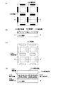
図1(A)には、本発明の接着体が形成される基板の上面図を示し、図1(B)には、図1(A)における破線AA‘で切断した際の断面図を示す。すなわち、接着体103は、図1(B)に示すように基板101上に形成された金属層102上に接して島状に形成される。なお、ここで形成される接着体は、金属層102と次に形成される酸化物層104との間に形成され、金属層102と酸化物層104との密着性を高めることができる。
1A shows a top view of a substrate on which the adhesive body of the present invention is formed, and FIG. 1B shows a cross-sectional view taken along the broken line AA ′ in FIG. 1A. . That is, the adhesive body 103 is formed in an island shape in contact with the
基板101に用いる材料としては、石英基板やガラス基板等を用いることができるが、後の工程において基板上に形成された素子形成層(TFTを含む)を基板から剥離する際に、その強度等が不十分である場合には、複数の基板を貼り合わせて用いることもできる。 As a material used for the substrate 101, a quartz substrate, a glass substrate, or the like can be used. However, when an element formation layer (including a TFT) formed on the substrate is peeled from the substrate in a later step, the strength, etc. Can be used by bonding a plurality of substrates together.
なお、金属層102を形成する材料としては、タングステン(W)、モリブデン(Mo)、テクネチウム(Tc)、レニウム(Re)、ルテニウム(Ru)、オスミウム(Os)、ロジウム(Rh)、イリジウム(Ir)、パラジウム(Pd)、白金(Pt)、銀(Ag)、または金(Au)から選ばれた元素、前記元素を主成分とする合金、または窒化物(例えば、窒化チタン、窒化タングステン、窒化タンタル、窒化モリブデン)を単層、または積層して用いることができる。
As a material for forming the
また、金属層102の上に形成される接着体103は、酸化物層104の上に形成されるTFTの周囲に形成される。すなわち、図1(A)に示すように、接着体103が形成された後、点線で覆われた領域105にTFTが形成される。なお、接着体103の配置、及び形状については、図1(A)示すものに限られることはなく適宜設計することができる。
In addition, the adhesive body 103 formed on the
なお、接着体103は、基板から素子形成層(TFTを含む)を剥離しやすくするために基板101上に形成される金属層102と密着性の高い材料からなり、具体的には、金属層102と接して形成されることにより金属層102中の金属と反応して金属化合物や合金を形成する材料、例えば、シリサイドを形成する珪素の他、ゲルマニウム、炭素、硼素、マグネシウム、アルミニウム、チタン、タンタル、鉄、コバルト、ニッケル、マンガン等の金属材料を用いることにより形成される。
Note that the bonding body 103 is made of a material having high adhesion to the
また、接着体103は、CVD(Chemical Vapor Deposition)法、スパッタリング法、蒸着法等の成膜法により成膜した後、これをパターンニングし、形成することができる。 Further, the adhesive body 103 can be formed by forming a film by a film forming method such as a CVD (Chemical Vapor Deposition) method, a sputtering method, or a vapor deposition method, and then patterning it.
また、本発明における酸化物層には、酸化珪素、酸化窒化珪素(SiOxNy)、窒化珪素等を用いることができ、スパッタリング法、CVD法等により成膜することができる。 In addition, silicon oxide, silicon oxynitride (SiO x N y ), silicon nitride, or the like can be used for the oxide layer in the present invention, and the oxide layer can be formed by a sputtering method, a CVD method, or the like.
また、本発明において、酸化物層104上に半導体素子であるTFT106を形成した後、図1(C)及び図1(D)に示すように、接着体が除去される。なお、図1(C)には、TFT106が形成された基板の上面図を示し、図1(D)には、図1(C)における破線BB‘で切断した際の断面図を示す。接着体103の除去方法としては、エッチング法(ドライエッチング法、ウエットエッチング法)を用いることができ、素子形成層107における層間絶縁膜および酸化物層104の一部と共に接着体103が除去される。すなわち、図1(C)の領域a(111)は、接着体103が除去された部分を示す。
In the present invention, after the TFT 106 which is a semiconductor element is formed over the
なお、接着体103を除去することにより、接着体103により高められていた基板101上の金属層102と酸化物層104との密着力は、低下する。
Note that by removing the adhesive 103, the adhesion between the
次に、TFT106を含む素子形成層107の上に接着層(第1の接着層ともいう)109を介して補助基板(第2の基板ともいう)110を貼り付けた後、物理的な力を加えることにより、素子形成層107および補助基板110を基板101から分離させることができる。なお、この場合、基板101上の金属層102と酸化物層104との界面において剥離することができる。以下、接着剤によって形成される層を接着層とする。
Next, after an auxiliary substrate (also referred to as a second substrate) 110 is attached to the
また、本発明では、上記接着体103を除去する際に形成された開口部を絶縁材料により埋めることもできる。なお、ここで用いる絶縁材料としては、有機絶縁材料であっても、無機絶縁材料であってもよい。具体的には、無機絶縁材料として、酸化珪素、窒化珪素、酸化窒化珪素などを用いることができ、有機絶縁材料として、アクリル(感光性アクリルを含む)、ポリアクリル(感光性ポリアクリルを含む)、ポリイミド、ポリアミド、BCB(ベンゾシクロブテン)等を用いることができる。 In the present invention, the opening formed when the adhesive 103 is removed can be filled with an insulating material. Note that the insulating material used here may be an organic insulating material or an inorganic insulating material. Specifically, silicon oxide, silicon nitride, silicon oxynitride, or the like can be used as the inorganic insulating material, and acrylic (including photosensitive acrylic) or polyacrylic (including photosensitive polyacrylic) as the organic insulating material. , Polyimide, polyamide, BCB (benzocyclobutene) and the like can be used.
また、接着層(第1の接着層)109には、後で補助基板(第2の基板)110を素子形成層107から剥離することのできる材料を用いることとする。例えば、紫外線を照射したり、加熱したりすることにより、接着力が低下するような接着材料を用いる。また、接着材料としては、両面テープ等を用いることもできる。さらに、補助基板(第2の基板)110を剥がした後、接着層(第1の接着層)109の残りを除去しやすくするため、素子形成層107と接着層(第1の接着層)109との間に水溶性の有機樹脂からなる膜を形成しておくこともできる。この場合、水洗して水溶性の有機樹脂からなる膜を除去することにより、同時に接着層(第1の接着層)109の残りを除去することができる。
For the adhesive layer (first adhesive layer) 109, a material that can later peel off the auxiliary substrate (second substrate) 110 from the
素子形成層107に補助基板110を貼り付けた後、基板101から素子形成層107を補助基板110と共に剥離する。このとき、基板101上の金属層102と、酸化物層104との間で剥離することができる。そして、剥離した素子形成層107を別の基板(第3の基板ともいう)、例えば、プラスチック等の可撓性基板上に接着層(第2の接着層ともいう)(ここでは図示しない)を用いて貼り付ける。
After the auxiliary substrate 110 is attached to the
なお、上記プラスチック等の可撓性基板としては、熱可塑性や熱硬化性の合成樹脂を用いることができる。例えば、ポリエチレン、ポリプロピレン、ポリスチレン、ポリアミド、ポリイミド、ポリアミドイミド、ポリカーボネート(PC)、アクリル系樹脂、ナイロン、ポリメチルメタクリレート、アクリル−スチレン共重合体(AS樹脂)、ポリエチレンテレフタレート(PET)、ポリエチレンナフタレート(PEN)、ポリエーテルサルフォン(PES)、ポリイミドポリエチレン、ポリプロピレン、フッ素系樹脂、スチレン系樹脂、ポリオレフィン系樹脂、メラミン樹脂、フェノール樹脂、ノルボルネン樹脂等を用いることができる。 Note that as the flexible substrate such as the plastic, a thermoplastic or thermosetting synthetic resin can be used. For example, polyethylene, polypropylene, polystyrene, polyamide, polyimide, polyamideimide, polycarbonate (PC), acrylic resin, nylon, polymethyl methacrylate, acrylic-styrene copolymer (AS resin), polyethylene terephthalate (PET), polyethylene naphthalate (PEN), polyethersulfone (PES), polyimide polyethylene, polypropylene, fluorine resin, styrene resin, polyolefin resin, melamine resin, phenol resin, norbornene resin, and the like can be used.
また、接着層(第2の接着層)には、反応硬化型接着剤、熱硬化型接着剤、紫外線硬化型接着剤等の光硬化型接着剤、嫌気型接着剤などの各種硬化型接着剤等の接着剤を用いることができるが、作業効率の点から紫外線硬化型接着剤が好ましい。 In addition, the adhesive layer (second adhesive layer) includes various curable adhesives such as a reactive curable adhesive, a thermosetting adhesive, a photocurable adhesive such as an ultraviolet curable adhesive, and an anaerobic adhesive. However, from the viewpoint of work efficiency, an ultraviolet curable adhesive is preferable.
最後に、補助基板110を除去することにより本発明の転写が完了する。具体的には、紫外線を照射したり、加熱したりすることにより、接着層(第1の接着層)109の接着力を低下させ、基板(第3の基板)に貼り付けられた素子形成層107から補助基板110を剥離する。さらに、素子形成層107と接着層(第1の接着層)109との間に水溶性の有機樹脂からなる膜が形成されている場合には、水洗することにより水溶性の有機樹脂からなる膜、および接着層(第1の接着層)109の残りを除去することができる。
Finally, the transfer of the present invention is completed by removing the auxiliary substrate 110. Specifically, the element forming layer attached to the substrate (third substrate) is reduced by irradiating ultraviolet rays or heating to reduce the adhesive force of the adhesive layer (first adhesive layer) 109. The auxiliary substrate 110 is peeled from 107. Further, when a film made of a water-soluble organic resin is formed between the
[実施の形態2]
本発明の実施の形態について図14を用いて説明する。
[Embodiment 2]
An embodiment of the present invention will be described with reference to FIG.
図14(A)には、本発明の接着体が形成される基板の上面図を示し、図14(B)には、図14(A)における破線AA‘で切断した際の断面図を示す。すなわち、接着体3103は、図14(B)に示すように基板3101上に形成された金属層3102上に接して島状に形成される。なお、ここで形成される接着体は、次に形成される酸化物層3104との間に形成され、金属層3102と酸化物層3104との密着性を高めることができる。
14A shows a top view of a substrate on which the adhesive body of the present invention is formed, and FIG. 14B shows a cross-sectional view taken along the broken line AA ′ in FIG. 14A. . That is, the adhesive 3103 is formed in an island shape in contact with the
基板3101に用いる材料としては、石英基板やガラス基板等を用いることができるが、後の工程において基板上に形成された素子形成層(複数の集積回路を含む)を基板から剥離する際に、その強度等が不十分である場合には、複数の基板を貼り合わせて用いることもできる。 As a material used for the substrate 3101, a quartz substrate, a glass substrate, or the like can be used, but when an element formation layer (including a plurality of integrated circuits) formed over the substrate in a later step is peeled from the substrate, When the strength is insufficient, a plurality of substrates can be bonded together.
なお、金属層3102を形成する材料としては、タングステン(W)、モリブデン(Mo)、テクネチウム(Tc)、レニウム(Re)、ルテニウム(Ru)、オスミウム(Os)、ロジウム(Rh)、イリジウム(Ir)、パラジウム(Pd)、白金(Pt)、銀(Ag)、または金(Au)から選ばれた元素、前記元素を主成分とする合金、または窒化物(例えば、窒化チタン、窒化タングステン、窒化タンタル、窒化モリブデン)を単層、または積層して用いることができる。
Note that as a material for forming the
また、金属層3102の上に形成される接着体3103は、酸化物層3104の上に形成される複数のTFTからなる集積回路の周囲に形成される。すなわち、図14(A)に示すように、接着体3103が形成された後、点線で覆われた領域3105に複数のTFTで構成される集積回路が形成される。なお、接着体3103の配置、及び形状については、図14(A)示すものに限られることはなく適宜設計することができる。
In addition, the adhesive 3103 formed over the
なお、接着体3103は、基板から素子形成層(複数のTFTで構成された複数の集積回路を含む)を剥離しやすくするために基板3101上に形成される金属層3102と密着性の高い材料からなり、具体的には、金属層3102と接して形成されることにより金属層3102中の金属と反応して金属化合物や合金を形成する材料、例えば、シリサイドを形成する珪素の他、ゲルマニウム、炭素、硼素、マグネシウム、アルミニウム、チタン、タンタル、鉄、コバルト、ニッケル、マンガン等の金属材料を用いることにより形成される。
Note that the adhesive body 3103 is a material having high adhesion to the
また、接着体3103は、CVD(Chemical Vapor Deposition)法、スパッタリング法、蒸着法等の成膜法により成膜した後、これをパターンニングし、形成することができる。 The adhesive 3103 can be formed by forming a film by a film forming method such as a CVD (Chemical Vapor Deposition) method, a sputtering method, or a vapor deposition method, and then patterning the film.
また、本発明における酸化物層には、酸化珪素、酸化窒化珪素(SiOxNy)、窒化珪素等を用いることができ、スパッタリング法、CVD法等により成膜することができる。 In addition, silicon oxide, silicon oxynitride (SiO x N y ), silicon nitride, or the like can be used for the oxide layer in the present invention, and the oxide layer can be formed by a sputtering method, a CVD method, or the like.
また、本発明において、酸化物層3104上に複数のTFTからなる複数の集積回路3106を形成した後、図14(C)及び図14(D)に示すように、接着体3103が除去される。なお、図14(C)には、集積回路3106が形成された基板の上面図を示し、図14(D)には、図14(C)における破線BB‘で切断した際の断面図を示す。接着体3103の除去方法としては、エッチング法(ドライエッチング法、ウエットエッチング法)を用いることができ、素子形成層3107における層間絶縁膜および酸化物層3104の一部と共に接着体3103が除去される。すなわち、図14(C)の領域a(111)は、接着体3103が除去された部分を示す。
Further, in the present invention, after a plurality of
なお、接着体3103を除去することにより、接着体3103により高められていた基板3101上の金属層3102と酸化物層3104との密着力は、低下する。
Note that by removing the adhesive 3103, the adhesion between the
次に、集積回路3106を含む素子形成層3107の上に接着層(第1の接着層ともいう)3109を介して補助基板(第2の基板ともいう)3110を貼り付けた後、物理的な力を加えることにより、素子形成層3107および補助基板3110を基板3101から分離させることができる。なお、この場合、基板3101上の金属層3102と酸化物層3104との界面において剥離することができる。
Next, after an auxiliary substrate (also referred to as a second substrate) 3110 is attached to the
また、本発明では、上記接着体3103を除去する際に形成された開口部を絶縁材料により埋めることもできる。なお、ここで用いる絶縁材料としては、有機絶縁材料であっても、無機絶縁材料であってもよい。具体的には、無機絶縁材料として、酸化珪素、窒化珪素、酸化窒化珪素などを用いることができ、有機絶縁材料として、アクリル(感光性アクリルを含む)、ポリアクリル(感光性ポリアクリルを含む)、ポリイミド、ポリアミド、BCB(ベンゾシクロブテン)等を用いることができる。 In the present invention, the opening formed when the adhesive 3103 is removed can be filled with an insulating material. Note that the insulating material used here may be an organic insulating material or an inorganic insulating material. Specifically, silicon oxide, silicon nitride, silicon oxynitride, or the like can be used as the inorganic insulating material, and acrylic (including photosensitive acrylic) or polyacrylic (including photosensitive polyacrylic) as the organic insulating material. , Polyimide, polyamide, BCB (benzocyclobutene) and the like can be used.
また、接着層(第1の接着層)3109には、後で補助基板(第2の基板)3110を素子形成層3107から剥離することのできる材料を用いることとする。例えば、紫外線を照射したり、加熱したりすることにより、接着力が低下するような接着材料を用いる。また、接着材料としては、両面テープ等を用いることもできる。さらに、補助基板(第2の基板)3110を剥がした後、接着層(第1の接着層)3109の残りを除去しやすくするため、素子形成層3107と接着層(第1の接着層)3109との間に水溶性の有機樹脂からなる膜を形成しておくこともできる。この場合、水洗して水溶性の有機樹脂からなる膜を除去することにより、同時に接着層(第1の接着層)3109の残りを除去することができる。
For the adhesive layer (first adhesive layer) 3109, a material that can later peel the auxiliary substrate (second substrate) 3110 from the
素子形成層3107に補助基板3110を貼り付けた後、基板3101から素子形成層3107を補助基板3110と共に剥離する。このとき、基板3101上の金属層3102と、酸化物層3104との間で剥離することができる。そして、剥離した素子形成層3107を別の基板(第3の基板ともいう)、例えば、プラスチック等の可撓性基板上に接着層(第2の接着層ともいう)(ここでは図示しない)を用いて貼り付ける。
After the auxiliary substrate 3110 is attached to the
なお、上記プラスチック等の可撓性基板としては、熱可塑性や熱硬化性の合成樹脂を用いることができる。例えば、ポリエチレン、ポリプロピレン、ポリスチレン、ポリアミド、ポリイミド、ポリアミドイミド、ポリカーボネート(PC)、アクリル系樹脂、ナイロン、ポリメチルメタクリレート、アクリル−スチレン共重合体(AS樹脂)、ポリエチレンテレフタレート(PET)、ポリエチレンナフタレート(PEN)、ポリエーテルサルフォン(PES)、ポリイミドポリエチレン、ポリプロピレン、フッ素系樹脂、スチレン系樹脂、ポリオレフィン系樹脂、メラミン樹脂、フェノール樹脂、ノルボルネン樹脂等を用いることができる。 Note that as the flexible substrate such as the plastic, a thermoplastic or thermosetting synthetic resin can be used. For example, polyethylene, polypropylene, polystyrene, polyamide, polyimide, polyamideimide, polycarbonate (PC), acrylic resin, nylon, polymethyl methacrylate, acrylic-styrene copolymer (AS resin), polyethylene terephthalate (PET), polyethylene naphthalate (PEN), polyethersulfone (PES), polyimide polyethylene, polypropylene, fluorine resin, styrene resin, polyolefin resin, melamine resin, phenol resin, norbornene resin, and the like can be used.
また、接着層(第2の接着層)には、反応硬化型接着剤、熱硬化型接着剤、紫外線硬化型接着剤等の光硬化型接着剤、嫌気型接着剤などの各種硬化型接着剤等の接着剤を用いることができるが、作業効率の点から紫外線硬化型接着剤が好ましい。 In addition, the adhesive layer (second adhesive layer) includes various curable adhesives such as a reactive curable adhesive, a thermosetting adhesive, a photocurable adhesive such as an ultraviolet curable adhesive, and an anaerobic adhesive. However, from the viewpoint of work efficiency, an ultraviolet curable adhesive is preferable.
最後に、補助基板3110を除去することにより本発明の転写が完了する。具体的には、紫外線を照射したり、加熱したりすることにより、接着層(第1の接着層)3109の接着力を低下させ、基板(第3の基板)に貼り付けられた素子形成層3107から補助基板3110を剥離する。さらに、素子形成層3107と接着層(第1の接着層)3109との間に水溶性の有機樹脂からなる膜が形成されている場合には、水洗することにより水溶性の有機樹脂からなる膜、および接着層(第1の接着層)3109の残りを除去することができる。
Finally, the transfer of the present invention is completed by removing the auxiliary substrate 3110. Specifically, the element forming layer attached to the substrate (third substrate) is reduced by irradiating ultraviolet rays or heating to reduce the adhesive force of the adhesive layer (first adhesive layer) 3109. The auxiliary substrate 3110 is peeled from 3107. Further, in the case where a film made of a water-soluble organic resin is formed between the
以下に、本発明の実施例について説明する。 Examples of the present invention will be described below.
本実施例では、本発明の転写工程を含む作製方法について図2、図3を用いて説明する。 In this embodiment, a manufacturing method including the transfer process of the present invention will be described with reference to FIGS.
図2(A)において、第1の基板201上に金属層202が積層され、その上に複数の接着体203が形成される。 In FIG. 2A, a metal layer 202 is stacked over a first substrate 201, and a plurality of adhesive bodies 203 are formed thereover.
なお、本実施例において、第1の基板201としては、ガラス基板、石英基板を用いることができる。なお、ガラス基板としては、バリウムホウケイ酸ガラス、アルミノホウケイ酸ガラス、アルミノシリケートガラスなどを素材とするガラス基板を用いることができ、代表的には、コーニング社製の1737ガラス基板(歪み点667℃)、旭硝子社製のAN100(歪み点670℃)などが適用可能である。本実施例では、AN100を用いることとする。 In this embodiment, a glass substrate or a quartz substrate can be used as the first substrate 201. As the glass substrate, a glass substrate made of barium borosilicate glass, aluminoborosilicate glass, aluminosilicate glass, or the like can be used. Typically, a 1737 glass substrate (strain point 667 ° C.) manufactured by Corning Corporation. ), AN100 manufactured by Asahi Glass Co., Ltd. (distortion point: 670 ° C.) is applicable. In this embodiment, the AN 100 is used.
また、金属層202には、タングステン(W)、モリブデン(Mo)、テクネチウム(Tc)、レニウム(Re)、ルテニウム(Ru)、オスミウム(Os)、ロジウム(Rh)、イリジウム(Ir)、パラジウム(Pd)、白金(Pt)、銀(Ag)、または金(Au)から選ばれた元素、前記元素を主成分とする合金、または窒化物(例えば、窒化チタン、窒化タングステン、窒化タンタル、窒化モリブデン)を単層、または積層して用いることができるが、本実施例では、W(タングステン)を主成分とする金属層202を用いることとする。なお、金属層202の膜厚は10nm〜200nm、好ましくは50nm〜75nmとすればよい。 The metal layer 202 includes tungsten (W), molybdenum (Mo), technetium (Tc), rhenium (Re), ruthenium (Ru), osmium (Os), rhodium (Rh), iridium (Ir), palladium ( An element selected from Pd), platinum (Pt), silver (Ag), or gold (Au), an alloy containing the element as a main component, or a nitride (for example, titanium nitride, tungsten nitride, tantalum nitride, molybdenum nitride) In this embodiment, the metal layer 202 containing W (tungsten) as a main component is used. Note that the thickness of the metal layer 202 may be 10 nm to 200 nm, preferably 50 nm to 75 nm.
金属層202は、スパッタリング法、CVD法、蒸着法により形成することができるが、本実施例では、スパッタリング法により成膜することとする。また、スパッタリング法により金属層202を形成する場合には、第1の基板201を固定するため、第1の基板201の周縁部付近における膜厚が不均一になりやすい。そのため、ドライエッチングによって周縁部のみを除去することが好ましい。 The metal layer 202 can be formed by a sputtering method, a CVD method, or an evaporation method. In this embodiment, the metal layer 202 is formed by a sputtering method. In addition, when the metal layer 202 is formed by a sputtering method, the first substrate 201 is fixed, and thus the film thickness in the vicinity of the peripheral portion of the first substrate 201 tends to be nonuniform. Therefore, it is preferable to remove only the peripheral portion by dry etching.
金属層202の上に形成される接着体203は、非晶質シリコン膜を成膜した後、これをパターニングすることにより形成される。 The adhesive 203 formed on the metal layer 202 is formed by forming an amorphous silicon film and then patterning it.
次に、酸化物層204を形成する(図2(B))。本実施例では酸化シリコンからなる膜を酸化シリコンターゲットを用いたスパッタリング法により、膜厚150nm〜200nmで形成する。なお、酸化物層204の膜厚は、金属層202の膜厚の2倍以上とすることが望ましい。
Next, the
次に、酸化物層204上に素子形成層301が形成される(図2(C))。素子形成層301には、TFT(pチャネル型TFT、またはnチャネル型TFT)が複数形成され、これらのTFTを接続する配線211、絶縁膜(210、212)の他、これらのTFTと接続された素子(発光素子、液晶素子)が含まれるものとする。なお、TFTを含む素子形成層の作製方法は、本発明において特に限定されるものではなく、実施例5で示すような作製方法の他、公知の作製方法を組み合わせて用いることができる。なお、TFTは、酸化物層204上の半導体膜の一部に形成された不純物領域205およびチャネル形成領域206、絶縁膜207、およびゲート電極208により構成される。
Next, the
本実施例では、素子形成層301を形成する際に、少なくとも水素を含む材料膜(半導体膜または金属膜)を形成した後、水素を含む材料膜中に含まれる水素を拡散するための熱処理を行う。この熱処理は420℃以上であればよく、素子形成層301の形成プロセスとは別途行ってもよいし、兼用させて工程を省略してもよい。例えば、水素を含む材料膜として水素を含むアモルファスシリコン膜をCVD法により成膜した後、結晶化させるため500℃以上の熱処理を行えば、加熱によりポリシリコン膜が形成できると同時に水素の拡散を行うことができる。
In this embodiment, at the time of forming the
なお、この熱処理を行うことにより、金属層202と酸化物層204との間に結晶構造を有する金属酸化物からなる層(図示せず)が形成される。なお、金属層202上に接着体203を形成し、その上に酸化物層204を積層形成する際に、金属層202と酸化物層204との間に2nm〜5nm程度形成されるアモルファス状態の金属酸化物層(本実施例では酸化タングステン膜)も、この熱処理により結晶構造を形成し、金属酸化物からなる層(図示せず)を形成する。
By performing this heat treatment, a layer (not shown) made of a metal oxide having a crystal structure is formed between the metal layer 202 and the
なお、この金属酸化物からなる層(図示せず)が金属層202と酸化物層204との界面に形成されることにより、後の工程での基板と素子形成層との剥離が容易になる。なお、本実施例では、素子形成層301を形成する途中の熱処理において、金属酸化物からなる層が形成される場合について説明したが、本発明はこの方法に限られることはなく、金属層202および接着体203を形成した後、金属酸化物層を形成し、酸化物層204を形成する方法で行うこともできる。
Note that a layer (not shown) made of the metal oxide is formed at the interface between the metal layer 202 and the
一方、素子形成層301を形成する途中の熱処理により、接着体203と金属層202との密着性を高めることができる。すなわち、本実施例において、非晶質シリコン膜で形成された接着体203は、熱処理を加えることにより、先に形成された金属層202中のタングステン(W)と反応して、シリサイド(タングステンシリサイド:WSi2)を形成する。そのため、接着体203と金属層202との密着性が高められる。なお、本発明では、素子形成層301を形成する途中の熱処理により、金属層中の金属と接着体とを反応させる方法に限られることなく、金属層と接着体を形成した後、金属層中の金属と接着体とを反応させるための熱処理を素子形成層301の作製とは別に行うこともできる。
On the other hand, the adhesion between the adhesive 203 and the metal layer 202 can be improved by heat treatment in the middle of forming the
素子形成層301が完成したところで、接着体203を除去する。具体的には、ドライエッチング法により絶縁膜(207、209、210、212)および酸化物層204の一部と接着体203とをエッチングし、開口部213を形成する(図2(D))。
When the
例えば、絶縁膜(207、209、210、212)および酸化物層204をエッチングする場合であって、これらが、酸化珪素で形成されている場合には、炭化フッ素(CF4)を主成分とするエッチングガスを用いてドライエッチングを行い、また接着体203をエッチングする場合であって、接着体203が珪素で形成されており、金属層(例えばW)との反応にも拘わらずその一部に珪素を主成分とする部分が残っている場合には、これを臭化水素(HBr)および塩素(Cl2)を主成分とするエッチングガスを用いてエッチングすることができる。さらに、接着体203が珪素で形成されており、金属層(W)との反応によってその一部がシリサイド(WSi)を形成している場合には、これをフッ化硫黄(SF6)と臭化水素(HBr)を主成分とするエッチングガスを用いてエッチングすることができる。
For example, in the case where the insulating films (207, 209, 210, 212) and the
次に、素子形成層301上に有機樹脂層214を形成する。有機樹脂層214に用いる材料としては、水またはアルコール類に可溶な有機材料を用い、これを全面に塗布、硬化することにより形成する。この有機材料の組成としては、例えば、エポキシ系、アクリレート系、シリコン系等のいかなるものでもよい。具体的には、スピンコート法により水溶性樹脂(東亜合成製:VL−WSHL10)(膜厚30μm)を塗布し、仮硬化させるために2分間の露光を行ったあと、UV光を裏面から2.5分、表面から10分、合計12.5分の露光を行って本硬化させることにより有機樹脂層214が形成される(図2(E))。
Next, the
なお、後の剥離を行いやすくするために、金属層202と酸化物層204との界面(金属酸化物を含む層)における密着性を部分的に低下させる処理を行う。密着性を部分的に低下させる処理は、剥離しようとする領域の周縁に沿って金属層202または酸化物層204にレーザー光を部分的に照射する処理、或いは、剥離しようとする領域の周縁に沿って外部から局所的に圧力を加えて酸化物層204の層内または界面の一部分に損傷を与える処理である。具体的にはダイヤモンドペンなどで硬い針を垂直に押しつけて荷重をかけて動かせばよい。好ましくは、スクライバー装置を用い、押し込み量を0.1mm〜2mmとし、圧力をかけて動かせばよい。このように、剥離を行う前に剥離現象が生じやすくなるような部分、即ち、きっかけをつくることが重要であり、密着性を選択的(部分的)に低下させる前処理を行うことで、剥離不良がなくなり、さらに歩留まりも向上する。
Note that in order to facilitate subsequent peeling, treatment for partially reducing the adhesion at the interface between the metal layer 202 and the oxide layer 204 (a layer containing a metal oxide) is performed. The treatment for partially reducing the adhesion is performed by partially irradiating the metal layer 202 or the
次に、第1の接着層215を形成することにより、有機樹脂層214上に第1の接着層215を介して補助基板である第2の基板216を貼り付けることができる(図2(E))。なお、第1の接着層215を形成する材料としては、後の工程において、所定の処理を行うことにより接着性が弱まる公知の材料を用いることができるが、本実施例では、後の工程において、光照射により接着力が低下する感光性の両面テープを用いる場合について説明する。
Next, by forming the first adhesive layer 215, the second substrate 216 which is an auxiliary substrate can be attached to the
次に、第1の基板201を物理的手段により補助基板が貼り付けられた素子形成層301から引き剥がす。本実施例の場合には、金属層202と酸化物層204との界面(金属酸化物を含む層)部分において、比較的小さな力(例えば、人間の手、ノズルから吹付けられるガスの風圧、超音波等)で引き剥がすことができる。具体的には、酸化タングステン膜中、または酸化タングステン膜と酸化シリコン膜との界面、または酸化タングステン膜とタングステン膜との界面で分離させ、引き剥がすことができる。こうして、酸化物層204上に形成された素子形成層301を第1の基板201から分離することができる。剥離時の状態を図3(A)に示す。
Next, the first substrate 201 is peeled off from the
また、剥離により露出した表面には、金属酸化物を含む層の一部が残っており、これは、後の工程において、露出面を基板等に接着する際に密着性を低下させる原因となることから、露出面に残っている金属酸化物を含む層の一部を除去する処理を行うことが好ましい。なお、これらを除去するためには、アンモニア水溶液などのアルカリ性の水溶液や酸性水溶液などを用いることができる。 In addition, a part of the layer containing a metal oxide remains on the surface exposed by peeling, which causes a decrease in adhesion when the exposed surface is bonded to a substrate or the like in a later step. Therefore, it is preferable to perform a treatment for removing a part of the layer containing the metal oxide remaining on the exposed surface. In order to remove them, an alkaline aqueous solution such as an aqueous ammonia solution or an acidic aqueous solution can be used.
次に、第2の接着層217を形成し、第2の接着層217を介して第3の基板218と酸化物層204(及び素子形成層301)とを接着する(図3(B))。なお、第1の接着層215により接着された第2の基板216と有機樹脂層214との密着性よりも、第2の接着層217により接着された酸化物層204(及び素子形成層301)と第3の基板218との密着性の方が高いことが重要である。
Next, a second adhesive layer 217 is formed, and the
第3の基板218としては、可撓性基板(プラスチック基板)を用いることが好ましく、本実施例では、極性基のついたノルボルネン樹脂からなるARTON(JSR製)を用いることとする。
As the
また、第2の接着層217に用いる材料としては、反応硬化型接着剤、熱硬化型接着剤、紫外線硬化型接着剤等の光硬化型接着剤、嫌気型接着剤などの各種硬化型接着剤が挙げられる。さらに好ましくは、銀、ニッケル、アルミニウム、窒化アルミニウムからなる粉末、またはフィラーを含ませることにより、高い熱伝導性を持たせることがより好ましい。 The material used for the second adhesive layer 217 includes various curable adhesives such as a reactive curable adhesive, a thermosetting adhesive, a photocurable adhesive such as an ultraviolet curable adhesive, and an anaerobic adhesive. Is mentioned. More preferably, it is more preferable to provide high thermal conductivity by including powder or filler made of silver, nickel, aluminum, aluminum nitride.
次に、第2の基板216側から紫外線を照射することにより、第1の接着層215に用いている両面テープの接着力を低下させ、素子形成層301から第2の基板216を分離させる(図3(C))。さらに、本実施例では、露出した表面を水洗することにより、第1の接着層215および有機樹脂層214を溶かして除去することができ、図3(D)に示す構造を得ることができる。
Next, the adhesive force of the double-sided tape used for the first adhesive layer 215 is reduced by irradiating ultraviolet rays from the second substrate 216 side, and the second substrate 216 is separated from the element formation layer 301 ( FIG. 3 (C)). Further, in this embodiment, by washing the exposed surface with water, the first adhesive layer 215 and the
以上により、第1の基板201上に形成されたTFTを剥離し、別の基板(第3の基板218)上に転写することができる。 Through the above steps, the TFT formed over the first substrate 201 can be peeled off and transferred onto another substrate (third substrate 218).
本実施例では、本発明の転写工程を含む作製方法であって、実施例1とはその一部が異なる場合について図4、図5を用いて説明する。 In this embodiment, a manufacturing method including the transfer process of the present invention, which is partly different from Embodiment 1, will be described with reference to FIGS.
図4(A)において、第1の基板401上に金属層402が積層され、その上に複数の接着体403が形成される。 4A, a metal layer 402 is stacked over a first substrate 401, and a plurality of adhesive bodies 403 are formed thereover.
なお、本実施例において、第1の基板401としては、実施例1と同様のガラス基板(AN100)を用いることとする。また、金属層402についても実施例1と同様にW(タングステン)を主成分とする金属層を用いることとする。なお、金属層402は、スパッタリング法により成膜し、その膜厚は10nm〜200nm、好ましくは50nm〜75nmとすればよい。 In this embodiment, as the first substrate 401, the same glass substrate (AN100) as in Embodiment 1 is used. As for the metal layer 402, a metal layer mainly composed of W (tungsten) is used as in the first embodiment. Note that the metal layer 402 is formed by a sputtering method and has a thickness of 10 nm to 200 nm, preferably 50 nm to 75 nm.
金属層402の上に形成される接着体403は、非晶質シリコン膜を成膜した後、これをパターニングすることにより形成される。 The adhesive body 403 formed on the metal layer 402 is formed by forming an amorphous silicon film and then patterning it.
次に、酸化物層404を形成する(図4(B))。本実施例では酸化シリコンからなる膜を酸化シリコンターゲットを用いたスパッタリング法により、膜厚150nm〜200nmで形成する。なお、酸化物層404の膜厚は、金属層402の膜厚の2倍以上とすることが望ましい。 Next, the oxide layer 404 is formed (FIG. 4B). In this embodiment, a film made of silicon oxide is formed with a film thickness of 150 nm to 200 nm by a sputtering method using a silicon oxide target. Note that the thickness of the oxide layer 404 is preferably twice or more than the thickness of the metal layer 402.
次に、酸化物層404上に素子形成層501が形成される(図4(C))。素子形成層501には、TFT(pチャネル型TFT、またはnチャネル型TFT)が複数形成され、これらのTFTを接続する配線411、絶縁膜410の他、これらのTFTと接続された素子(発光素子、液晶素子)が含まれるものとする。なお、TFTを含む素子形成層の作製方法は、本発明において特に限定されるものではなく、実施例5で示すような作製方法の他、公知の作製方法を組み合わせて用いることができる。なお、TFTは、酸化物層404上の半導体膜の一部に形成された不純物領域405およびチャネル形成領域406、絶縁膜407、およびゲート電極408により構成される。
Next, an
本実施例でも実施例1の場合と同様に素子形成層501を形成する際に、少なくとも水素を含む材料膜(半導体膜または金属膜)を形成した後、水素を含む材料膜中に含まれる水素を拡散するための熱処理を行う。なお、この熱処理を行うことにより、金属層402と酸化物層404との間に結晶構造を有する金属酸化物からなる層(図示せず)が形成される。
In this embodiment as well, when forming the
なお、この金属酸化物からなる層(図示せず)が金属層402と酸化物層404との界面に形成されることにより、後の工程での基板と素子形成層との剥離が容易になる。 Note that a layer (not shown) made of the metal oxide is formed at the interface between the metal layer 402 and the oxide layer 404, so that the substrate and the element formation layer can be easily separated in a later step. .
一方、素子形成層501を形成する途中の熱処理により、接着体403と金属層402との密着性を高めることができる。
On the other hand, the adhesion between the adhesive 403 and the metal layer 402 can be increased by heat treatment in the middle of forming the
本実施例では、素子形成層501に含まれる配線411まで形成したところで、接着体403を除去する。具体的には、ドライエッチング法により絶縁膜410の一部と接着体403とをエッチングし、開口部412を形成する(図4(D))。
In this embodiment, the adhesive 403 is removed when the wiring 411 included in the
例えば、絶縁膜(407、409、410)および酸化物層404をエッチングする場合であって、これらが、酸化珪素で形成されている場合には、炭化フッ素(CF4)を主成分とするエッチングガスを用いてドライエッチングを行い、また接着体403をエッチングする場合であって、接着体403が珪素で形成されており、金属層(例えばW)との反応にも拘わらずその一部に珪素を主成分とする部分が残っている場合には、これを臭化水素(HBr)および塩素(Cl2)を主成分とするエッチングガスを用いてエッチングすることができる。さらに、接着体403が珪素で形成されており、金属層(W)との反応によってその一部がシリサイド(WSi)を形成している場合には、これをフッ化硫黄(SF6)と臭化水素(HBr)を主成分とするエッチングガスを用いてエッチングすることができる。 For example, in the case where the insulating films (407, 409, 410) and the oxide layer 404 are etched and these are formed of silicon oxide, the etching mainly includes fluorine carbide (CF 4 ). In the case where dry etching is performed using a gas and the adhesive 403 is etched, the adhesive 403 is formed of silicon, and silicon is partially contained in spite of reaction with the metal layer (for example, W). If the main component remains, it can be etched using an etching gas containing hydrogen bromide (HBr) and chlorine (Cl 2 ) as main components. Further, when the bonding body 403 is formed of silicon and a part thereof forms silicide (WSi) by the reaction with the metal layer (W), this is treated with sulfur fluoride (SF 6 ) and odor. Etching can be performed using an etching gas mainly containing hydrogen fluoride (HBr).
次に、開口部412を埋め、素子形成層501の表面を平坦化するために絶縁膜413を形成する(図4(E))。なお、本実施例では、プラズマCVD法により形成された膜厚1〜3μmの窒化酸化シリコン膜を用いる。勿論、この絶縁膜は窒化酸化シリコン膜に限定されるものでなく、窒化シリコン、酸化シリコンといった絶縁材料や、アクリル、ポリイミド、ポリアミドなどの有機絶縁材料からなる単層構造や、これらを組み合わせた積層構造としても良い。
Next, an insulating film 413 is formed to fill the
なお、絶縁膜413により素子形成層501の表面を平坦化した後の工程である(1)素子形成層501の上に有機樹脂層を形成し、その上に第1の接着層を介して補助基板である第2の基板を貼り付ける工程、(2)素子形成層501から第1の基板401を物理的手段により補助基板(第2の基板)が貼り付けられた素子形成層501から引き剥がす工程、(3)第2の接着層を形成し、第2の接着層を介して第3の基板と酸化物層(及び素子形成層)とを接着する工程、および(4)素子形成層から第2の基板を分離させる工程、については実施例1に示すものと同様の材料を用いて、同様の方法により形成することができるので説明は省略することとする。
Note that (1) an organic resin layer is formed on the
以上により、素子形成層501が第2の接着層417を介して第3の基板418上に転写された図5(A)に示す構造を得ることができる。
Thus, the structure shown in FIG. 5A in which the
また、本実施例では、図4(D)において開口部412を形成した後、絶縁膜419を形成することにより、図5(B)に示す構造を形成しても良い。
In this embodiment, the structure shown in FIG. 5B may be formed by forming the insulating film 419 after forming the
以上により、第1の基板401上に形成されたTFTを剥離し、別の基板(第3の基板418)上に転写することができる。 As described above, the TFT formed over the first substrate 401 can be peeled off and transferred onto another substrate (third substrate 418).
本実施例では、本発明の転写工程を含む作製方法であって、実施例1や実施例2とはその一部が異なる場合について図6、図7を用いて説明する。 In this embodiment, a manufacturing method including a transfer process according to the present invention, which is partially different from Embodiments 1 and 2, will be described with reference to FIGS.
図6(A)において、第1の基板601上に金属層602が積層され、その上に酸化物層603が形成される。 6A, a metal layer 602 is stacked over a first substrate 601, and an oxide layer 603 is formed thereover.
なお、本実施例において、第1の基板601としては、実施例1と同様のガラス基板(AN100)を用いることとする。また、金属層602についても実施例1と同様にW(タングステン)を主成分とする金属層602を用いることとする。なお、金属層402は、スパッタリング法により成膜し、その膜厚は10nm〜200nm、好ましくは50nm〜75nmとすればよい。 In this embodiment, the same glass substrate (AN100) as that in Embodiment 1 is used as the first substrate 601. As for the metal layer 602, a metal layer 602 containing W (tungsten) as a main component is used as in the first embodiment. Note that the metal layer 402 is formed by a sputtering method and has a thickness of 10 nm to 200 nm, preferably 50 nm to 75 nm.
金属層602の上に形成される酸化物層603は、酸化シリコンからなる膜を酸化シリコンターゲットを用いたスパッタリング法により、膜厚150nm〜200nmで形成する。なお、酸化物層603の膜厚は、金属層602の膜厚の2倍以上とすることが望ましい。また、本実施例において、酸化物層603は、パターニングにより複数の島状に分離形成される。 As the oxide layer 603 formed over the metal layer 602, a film made of silicon oxide is formed with a thickness of 150 nm to 200 nm by a sputtering method using a silicon oxide target. Note that the thickness of the oxide layer 603 is preferably greater than or equal to twice the thickness of the metal layer 602. In this embodiment, the oxide layer 603 is separated and formed into a plurality of islands by patterning.
次に、酸化物層603を覆って、半導体膜604が形成される。本実施例では、非晶質シリコン膜をプラズマCVD法により成膜することにより形成される(図6(A))。そして、この半導体膜604をパターニングすることにより、酸化物層603上に形成される半導体a(605)、分離形成された2つの酸化物層603の間に形成された半導体b(606)が得られる。なお、ここで形成される半導体a(605)は、後で形成されるTFTの不純物領域およびチャネル形成領域となり、半導体b(606)が、本発明における接着体となる。 Next, a semiconductor film 604 is formed so as to cover the oxide layer 603. In this embodiment, an amorphous silicon film is formed by a plasma CVD method (FIG. 6A). Then, by patterning the semiconductor film 604, a semiconductor a (605) formed over the oxide layer 603 and a semiconductor b (606) formed between two separated oxide layers 603 are obtained. It is done. The semiconductor a (605) formed here becomes an impurity region and a channel formation region of a TFT to be formed later, and the semiconductor b (606) becomes an adhesive body in the present invention.
すなわち、本発明では、TFTの一部を形成する半導体a(605)と、接着体を形成する半導体b(606)が同時に形成される点に特徴がある。 That is, the present invention is characterized in that the semiconductor a (605) that forms part of the TFT and the semiconductor b (606) that forms the adhesive are formed at the same time.
次に、半導体a(605)を一部に含む素子形成層701が形成される(図6(C))。素子形成層701には、TFT(pチャネル型TFT、またはnチャネル型TFT)が複数形成され、これらのTFTを接続する配線613、絶縁膜612の他、これらのTFTと接続された素子(発光素子、液晶素子)が含まれるものとする。なお、TFTを含む素子形成層の作製方法は、本発明において特に限定されるものではなく、実施例5で示すような作製方法の他、公知の作製方法を組み合わせて用いることができる。なお、TFTは、酸化物層603上の半導体a(605)の一部に形成された不純物領域607およびチャネル形成領域608、ゲート絶縁膜609、およびゲート電極610により構成される。
Next, an
本実施例でも実施例1の場合と同様に素子形成層701を形成する際に、少なくとも水素を含む材料膜(半導体膜または金属膜)を形成した後、水素を含む材料膜中に含まれる水素を拡散するための熱処理を行う。なお、この熱処理を行うことにより、金属層602と酸化物層603との間に結晶構造を有する金属酸化物からなる層(図示せず)が形成される。 In this embodiment as well, in the same manner as in Embodiment 1, after forming a material film (semiconductor film or metal film) containing at least hydrogen, hydrogen contained in the material film containing hydrogen is formed. A heat treatment for diffusing is performed. Note that by this heat treatment, a layer (not shown) made of a metal oxide having a crystal structure is formed between the metal layer 602 and the oxide layer 603.
なお、この金属酸化物からなる層(図示せず)が金属層602と酸化物層603との界面に形成されることにより、後の工程での第1の基板601と素子形成層701との剥離が容易になる。
Note that a layer (not shown) made of the metal oxide is formed at the interface between the metal layer 602 and the oxide layer 603, whereby the first substrate 601 and the
一方、素子形成層701を形成する途中の熱処理により、接着体である半導体b(606)と金属層602との密着性を高めることができる。
On the other hand, the adhesion between the semiconductor b (606), which is an adhesive, and the metal layer 602 can be increased by heat treatment in the middle of forming the
本実施例では、素子形成層701に含まれる配線613まで形成したところで、半導体b(606)を除去する(図6(D))。具体的には、ドライエッチング法により絶縁膜612の一部と半導体b(606)とをエッチングし、開口部614を形成する。
In this example, when the wiring 613 included in the
例えば、絶縁膜(609、611、612)および酸化物層603をエッチングする場合であって、これらが、酸化珪素で形成されている場合には、炭化フッ素(CF4)を主成分とするエッチングガスを用いてドライエッチングを行い、また接着体である半導体b(606)をエッチングする場合であって、半導体b(606)が珪素で形成されており、金属層(例えばW)との反応にも拘わらずその一部に珪素を主成分とする部分が残っている場合には、これを臭化水素(HBr)および塩素(Cl2)を主成分とするエッチングガスを用いてエッチングすることができる。さらに、半導体b(606)が珪素で形成されており、金属層(W)との反応によってその一部がシリサイド(WSi)を形成している場合には、これをフッ化硫黄(SF6)と臭化水素(HBr)を主成分とするエッチングガスを用いてエッチングすることができる。 For example, in the case where the insulating films (609, 611, 612) and the oxide layer 603 are etched and these are formed of silicon oxide, the etching mainly includes fluorine carbide (CF 4 ). In the case where dry etching is performed using a gas and the semiconductor b (606) which is an adhesive is etched, the semiconductor b (606) is formed of silicon and is used for reaction with a metal layer (for example, W). However, in the case where a part mainly composed of silicon remains in part, it can be etched using an etching gas mainly composed of hydrogen bromide (HBr) and chlorine (Cl 2 ). it can. Further, when the semiconductor b (606) is formed of silicon and a part thereof forms silicide (WSi) by reaction with the metal layer (W), this is converted to sulfur fluoride (SF 6 ). Etching can be performed using an etching gas mainly containing hydrogen bromide (HBr).
次に、開口部614を埋め、素子形成層701の表面を平坦化するために絶縁膜615を形成する(図6(E))。なお、本実施例では、プラズマCVD法により形成された膜厚1〜3μmの窒化酸化シリコン膜を用いる。勿論、この絶縁膜は窒化酸化シリコン膜に限定されるものでなく、窒化シリコン、窒化シリコン、酸化シリコンといった絶縁材料や、アクリル、ポリイミド、ポリアミドなどの有機絶縁材料からなる単層構造や、これらを組み合わせた積層構造としても良い。
Next, an insulating film 615 is formed to fill the
なお、絶縁膜615により素子形成層701の表面を平坦化した後の工程である(1)素子形成層701の上に有機樹脂層を形成し、その上に第1の接着層を介して補助基板である第2の基板を貼り付ける工程、(2)素子形成層701から第1の基板601を物理的手段により補助基板(第2の基板)が貼り付けられた素子形成層701から引き剥がす工程、(3)第2の接着層を形成し、第2の接着層を介して第3の基板と酸化物層(及び素子形成層)とを接着する工程、および(4)素子形成層から第2の基板を分離させる工程、については実施例1に示すものと同様の材料を用いて、同様の方法により形成することができるので説明は省略することとする。
Note that (1) an organic resin layer is formed on the
以上により、素子形成層701が第2の接着層617を介して第3の基板618上に転写された図7(A)に示す構造を得ることができる。
Through the above, a structure illustrated in FIG. 7A in which the
また、本実施例では、図6(D)において開口部614を形成した後、絶縁膜800を形成することにより、図7(B)に示す構造を形成しても良い。
In this embodiment, the structure shown in FIG. 7B may be formed by forming the insulating film 800 after forming the
以上により、第1の基板601上に形成されたTFTを剥離し、別の基板(第3の基618板)上に転写することができる。 Thus, the TFT formed over the first substrate 601 can be peeled off and transferred onto another substrate (third base 618 plate).
本実施例では、本発明における接着体の配置およびその形状について、図8を用いて説明する。 In this example, the arrangement and shape of the adhesive in the present invention will be described with reference to FIG.
本発明では、図8(A)に示すように基板801上に形成された素子形成層802が、物理的手段によって剥離され、別の基板上に貼付けられることにより、転写が行われる。なお、図8(A)の場合には、素子形成層802は、矢印の方向に剥離されるものとする。 In the present invention, as shown in FIG. 8A, the element formation layer 802 formed on the substrate 801 is peeled off by physical means and pasted on another substrate for transfer. Note that in the case of FIG. 8A, the element formation layer 802 is peeled in the direction of the arrow.
そこで、素子形成層802に形成される接着体の配置および形状について、素子形成層802の一部である領域803に素子形成層802の作製途中に形成され、剥離直前に除去される接着体の配置および形状の一例を図8(B)〜図8(D)に示す。 Therefore, regarding the arrangement and shape of the adhesive formed on the element formation layer 802, the adhesive formed on the region 803, which is a part of the element formation layer 802, is formed during the production of the element formation layer 802 and removed immediately before peeling. An example of the arrangement and shape is shown in FIGS. 8B to 8D.
図8(B)では、TFT804が複数形成される領域803において、剥離方向XX’に配列されるTFT804の間に四角形状の接着体805が形成される場合について示す。なお、この場合、四角形状の接着体805が長方形を有し、剥離方向AA’と平行に長方形の長辺が並ぶように配置されるのがより好ましい。このように接着体805を四角形状とすることにより、接着体805を除去した後、素子形成層802を基板801から容易に剥離することができる。 FIG. 8B shows a case where a rectangular adhesive body 805 is formed between TFTs 804 arranged in the peeling direction XX ′ in a region 803 where a plurality of TFTs 804 are formed. In this case, it is more preferable that the quadrangular adhesive body 805 has a rectangular shape and is arranged so that the long sides of the rectangular shape are aligned in parallel to the peeling direction AA ′. Thus, by making the adhesive body 805 into a quadrangular shape, the element formation layer 802 can be easily peeled from the substrate 801 after the adhesive body 805 is removed.
図8(C)では、TFT806が複数形成される領域803において、剥離方向AA’に配列されるTFT806の間に三角形状の接着体807が形成される場合について示す。なお、この場合、三角形状の接着体807の底辺が、剥離方向XX’と垂直になるように配置されるのがより好ましい。このように接着体807を三角形状とした場合にも、接着体807を除去した後、素子形成層802を基板801から容易に剥離することができる。 FIG. 8C illustrates a case where a triangular adhesive body 807 is formed between TFTs 806 arranged in the peeling direction AA ′ in a region 803 where a plurality of TFTs 806 are formed. In this case, it is more preferable that the triangular adhesive body 807 is arranged so that the bottom side thereof is perpendicular to the peeling direction XX ′. Thus, even when the adhesive body 807 has a triangular shape, the element formation layer 802 can be easily peeled from the substrate 801 after the adhesive body 807 is removed.
図8(D)では、TFT808が複数形成される領域803において、剥離方向XX’に複数配列されるTFT808の列と列との間にライン状の接着体809が形成される場合について示す。なお、この場合、ライン状の接着体809は、剥離方向XX’に複数のTFT808が配列されるのと同じ長さで形成しても良いが、TFT8081つ分の長さで形成しても良い。このように接着体809をライン状とした場合にも、接着体807を除去した後、素子形成層802を基板801から容易に剥離することができる。 FIG. 8D illustrates a case where a line-shaped adhesive body 809 is formed between rows of TFTs 808 arranged in the peeling direction XX ′ in a region 803 where a plurality of TFTs 808 are formed. In this case, the line-shaped adhesive body 809 may be formed with the same length as a plurality of TFTs 808 arranged in the peeling direction XX ′, or may be formed with a length corresponding to one TFT 8081. . Thus, even when the adhesive body 809 is formed in a line shape, the element formation layer 802 can be easily peeled from the substrate 801 after the adhesive body 807 is removed.
なお、本実施例で示した接着体の配置および形状は、本発明における好ましい一例に過ぎず、本発明の接着体の形状を何ら限定するものではない。 In addition, arrangement | positioning and the shape of the adhesive body shown by the present Example are only a preferable example in this invention, and do not limit the shape of the adhesive body of this invention at all.
本実施例では、同一基板上にnチャネル型TFT及びpチャネル型TFTを同時に作製する方法について、図9、図10を用いて説明する。 In this embodiment, a method for simultaneously manufacturing an n-channel TFT and a p-channel TFT on the same substrate will be described with reference to FIGS.
基板901上に金属層902が形成され、その上に接着体903が形成される。
A
本実施例では、基板901として、ガラス基板(#1737)を用い、金属層902には、実施例1と同様にタングステン(W)を主成分とする金属材料を用いる。なお、接着体903は、後で形成されるTFTの間に配置されるように所望の形状にパターニングされ、形成される。
In this embodiment, a glass substrate (# 1737) is used as the
次に金属層902および接着体903上に下地絶縁膜としても機能する酸化物層904を形成する。本実施例では、プラズマCVD法で成膜温度300℃、原料ガスSiH4、N2Oから作製される酸化窒化シリコン膜(組成比Si=32%、O=59%、N=7%、H=2%)を100nmの厚さに成膜することにより、酸化物層904を形成する。
Next, an
さらに、大気解放せず連続的にプラズマCVD法で成膜温度300℃、成膜ガスSiH4で非晶質構造を有する半導体層(ここでは非晶質シリコン層)を54nmの厚さで形成する。この非晶質シリコン層は水素を含んでおり、後の熱処理によって水素を拡散させ、物理的手段で酸化物層の層内、あるいは界面において剥離することができる。 Further, a semiconductor layer having an amorphous structure (here, an amorphous silicon layer) is formed with a thickness of 54 nm by a plasma CVD method and continuously with a film forming gas SiH 4 without being exposed to the atmosphere. . This amorphous silicon layer contains hydrogen, and can be peeled off in the oxide layer or at the interface by physical means by diffusing hydrogen by a subsequent heat treatment.
次に、重量換算で10ppmのニッケルを含む酢酸ニッケル塩溶液をスピナーで塗布する。塗布に代えてスパッタ法でニッケル元素を全面に散布する方法を用いてもよい。次いで、加熱処理を行い結晶化させて結晶構造を有する半導体膜(ここではポリシリコン層)を形成する。ここでは脱水素化のための熱処理(500℃、1時間)の後、結晶化のための熱処理(550℃、4時間)を行って結晶構造を有するシリコン膜を得る。また、この脱水素化のための熱処理(500℃、1時間)は、非晶質シリコン膜に含まれる水素を金属層902と酸化物層904との界面に拡散する熱処理を兼ねている。なお、ここではシリコンの結晶化を助長する金属元素としてニッケルを用いた結晶化技術を用いるが、他の公知の結晶化技術、例えば固相成長法やレーザー結晶化法を用いてもよい。
Next, a nickel acetate salt solution containing 10 ppm of nickel in terms of weight is applied with a spinner. Instead of coating, a method of spreading nickel element over the entire surface by sputtering may be used. Next, heat treatment is performed for crystallization, so that a semiconductor film having a crystal structure (here, a polysilicon layer) is formed. Here, after heat treatment for dehydrogenation (500 ° C., 1 hour), heat treatment for crystallization (550 ° C., 4 hours) is performed to obtain a silicon film having a crystal structure. The heat treatment for dehydrogenation (500 ° C., 1 hour) also serves as heat treatment for diffusing hydrogen contained in the amorphous silicon film to the interface between the
次に、結晶構造を有するシリコン膜表面の酸化膜を希フッ酸等で除去した後、結晶化率を高め、結晶粒内に残される欠陥を補修するためのレーザー光(XeCl:波長308nm)の照射を大気中、または酸素雰囲気中で行う。レーザー光には波長400nm以下のエキシマレーザー光や、YAGレーザーの第2高調波、第3高調波を用いる。ここでは、繰り返し周波数10〜1000Hz程度のパルスレーザー光を用い、当該レーザー光を光学系にて100〜500mJ/cm2に集光し、90〜95%のオーバーラップ率をもって照射し、シリコン膜表面を走査させればよい。ここでは、繰り返し周波数30Hz、エネルギー密度470mJ/cm2でレーザー光の照射を大気中で行う。 Next, after removing the oxide film on the surface of the silicon film having a crystal structure with dilute hydrofluoric acid or the like, laser light (XeCl: wavelength 308 nm) for increasing the crystallization rate and repairing defects left in the crystal grains Irradiation is performed in air or in an oxygen atmosphere. As the laser light, excimer laser light having a wavelength of 400 nm or less, and second harmonic and third harmonic of YAG laser are used. Here, a pulsed laser beam having a repetition frequency of about 10 to 1000 Hz is used, the laser beam is condensed to 100 to 500 mJ / cm 2 by an optical system, and irradiated with an overlap rate of 90 to 95%, and the silicon film surface May be scanned. Here, laser light irradiation is performed in the atmosphere at a repetition frequency of 30 Hz and an energy density of 470 mJ / cm 2 .
なお、大気中、または酸素雰囲気中で行うため、レーザー光の照射により表面に酸化膜が形成される。なお、ここではパルスレーザーを用いる例を示したが、連続発振のレーザーを用いてもよく、非晶質半導体膜の結晶化に際し、大粒径に結晶を得るためには、連続発振が可能な固体レーザーを用い、基本波の第2高調波〜第4高調波を適用するのが好ましい。代表的には、Nd:YVO4レーザー(基本波1064nm)の第2高調波(532nm)や第3高調波(355nm)を適用すればよい。連続発振のレーザーを用いる場合には、出力10Wの連続発振のYVO4レーザから射出されたレーザー光を非線形光学素子により高調波に変換する。また、共振器の中にYVO4結晶と非線形光学素子を入れて、高調波を射出する方法もある。そして、好ましくは光学系により照射面にて矩形状または楕円形状のレーザー光に成形して、被処理体に照射する。このときのエネルギー密度は0.01〜100MW/cm2程度(好ましくは0.1〜10MW/cm2)が必要である。そして、10〜2000cm/s程度の速度でレーザー光に対して相対的に半導体膜を移動させて照射すればよい。 Note that since the reaction is performed in the air or in an oxygen atmosphere, an oxide film is formed on the surface by laser light irradiation. Although an example using a pulsed laser is shown here, a continuous wave laser may be used, and in order to obtain a crystal with a large grain size when crystallizing an amorphous semiconductor film, continuous wave is possible. It is preferable to apply a second to fourth harmonic of the fundamental wave using a solid-state laser. Typically, a second harmonic (532 nm) or a third harmonic (355 nm) of an Nd: YVO 4 laser (fundamental wave 1064 nm) may be applied. In the case of using a continuous wave laser, laser light emitted from a continuous wave YVO 4 laser having an output of 10 W is converted into a harmonic by a non-linear optical element. There is also a method of emitting harmonics by putting a YVO 4 crystal and a nonlinear optical element in a resonator. Preferably, the laser beam is shaped into a rectangular or elliptical shape on the irradiation surface by an optical system, and the object to be processed is irradiated. At this time, the energy density of approximately 0.01 to 100 MW / cm 2 (preferably 0.1 to 10 MW / cm 2) is required. Then, irradiation may be performed by moving the semiconductor film relative to the laser light at a speed of about 10 to 2000 cm / s.
次に、上記レーザー光の照射により形成された酸化膜に加え、オゾン水で表面を120秒処理して合計1〜5nmの酸化膜からなるバリア層を形成する。本実施の形態ではオゾン水を用いてバリア層を形成するが、酸素雰囲気下の紫外線の照射で結晶構造を有する半導体膜の表面を酸化する方法や酸素プラズマ処理により結晶構造を有する半導体膜の表面を酸化する方法やプラズマCVD法やスパッタ法や蒸着法などで1〜10nm程度の酸化膜を堆積してバリア層を形成してもよい。また、バリア層を形成する前にレーザー光の照射により形成された酸化膜を除去してもよい。 Next, in addition to the oxide film formed by the laser beam irradiation, the surface is treated with ozone water for 120 seconds to form a barrier layer made of an oxide film having a total thickness of 1 to 5 nm. In this embodiment mode, a barrier layer is formed using ozone water. However, a method of oxidizing a surface of a semiconductor film having a crystal structure by irradiation with ultraviolet rays in an oxygen atmosphere or a surface of a semiconductor film having a crystal structure by oxygen plasma treatment A barrier layer may be formed by depositing an oxide film having a thickness of about 1 to 10 nm by a method such as oxidation, plasma CVD, sputtering, or vapor deposition. Further, the oxide film formed by laser light irradiation may be removed before forming the barrier layer.
次に、バリア層上にスパッタリング法にてゲッタリングサイトとなるアルゴン元素を含む非晶質シリコン膜を10nm〜400nm、ここでは膜厚100nmで成膜する。本実施例では、アルゴン元素を含む非晶質シリコン膜は、シリコンターゲットを用いてアルゴンを含む雰囲気下で形成する。プラズマCVD法を用いてアルゴン元素を含む非晶質シリコン膜を形成する場合、成膜条件は、モノシランとアルゴンの流量比(SiH4:Ar)を1:99とし、成膜圧力を6.665Pa(0.05Torr)とし、RFパワー密度を0.087W/cm2とし、成膜温度を350℃とする。 Next, an amorphous silicon film containing an argon element serving as a gettering site is formed with a thickness of 10 to 400 nm, here 100 nm, over the barrier layer by a sputtering method. In this embodiment, the amorphous silicon film containing an argon element is formed in an atmosphere containing argon using a silicon target. In the case where an amorphous silicon film containing an argon element is formed using a plasma CVD method, the film formation conditions are a monosilane / argon flow rate ratio (SiH 4 : Ar) of 1:99 and a film formation pressure of 6.665 Pa. (0.05 Torr), RF power density is 0.087 W / cm 2, and film forming temperature is 350 ° C.
その後、650℃に加熱された炉に入れて3分の熱処理を行いゲッタリングして、結晶構造を有する半導体膜中のニッケル濃度を低減する。炉に代えてランプアニール装置を用いてもよい。 After that, heat treatment is performed for 3 minutes in a furnace heated to 650 ° C., and gettering is performed to reduce the nickel concentration in the semiconductor film having a crystal structure. A lamp annealing apparatus may be used instead of the furnace.
次に、バリア層をエッチングストッパーとして、ゲッタリングサイトであるアルゴン元素を含む非晶質シリコン膜を選択的に除去した後、バリア層を希フッ酸で選択的に除去する。なお、ゲッタリングの際、ニッケルは酸素濃度の高い領域に移動しやすい傾向があるため、酸化膜からなるバリア層をゲッタリング後に除去することが望ましい。 Next, the amorphous silicon film containing an argon element which is a gettering site is selectively removed using the barrier layer as an etching stopper, and then the barrier layer is selectively removed with dilute hydrofluoric acid. Note that during gettering, nickel tends to move to a region with a high oxygen concentration, and thus it is desirable to remove the barrier layer made of an oxide film after gettering.
次いで、得られた結晶構造を有するシリコン膜(ポリシリコン膜とも呼ばれる)の表面にオゾン水で薄い酸化膜を形成した後、レジストからなるマスクを形成し、所望の形状にエッチング処理して島状に分離された半導体層905、906を形成する。半導体層905、906を形成した後、レジストからなるマスクを除去する(図9(A))。
Next, after forming a thin oxide film with ozone water on the surface of the obtained silicon film having a crystal structure (also called a polysilicon film), a mask made of resist is formed and etched into a desired shape to form islands. The separated
次に、フッ酸を含むエッチャントで酸化膜を除去すると同時にシリコン膜(半導体層905、906)の表面を洗浄した後、ゲート絶縁膜907となるシリコンを主成分とする絶縁膜を形成する。本実施例では、プラズマCVD法により115nmの厚さで酸化シリコン膜を形成する(図9(B))。
Next, the oxide film is removed with an etchant containing hydrofluoric acid, and at the same time, the surface of the silicon film (semiconductor layers 905 and 906) is washed, and then an insulating film containing silicon as a main component to be the
さらに、ゲート絶縁膜907上に膜厚20〜100nmの第1の導電膜908と、膜厚100〜400nmの第2の導電膜909とを積層形成する。本実施例では、ゲート絶縁膜907上に第1の導電膜908となる膜厚50nmの窒化タンタル膜、第2の導電膜909となる膜厚370nmのタングステン膜を順次積層する。
Further, a first
なお、第1の導電膜908及び第2の導電膜909を形成する導電性材料としてはTa、W、Ti、Mo、Al、Cuから選ばれた元素、または前記元素を主成分とする合金材料もしくは化合物材料を用いることができる。また、第1の導電膜908及び第2の導電膜909としてリン等の不純物元素をドーピングした多結晶シリコン膜に代表される半導体膜や、AgPdCu合金を用いてもよい。また、2層構造に限定されず、例えば、膜厚50nmのタングステン膜、膜厚500nmのアルミニウムとシリコンの合金(Al−Si)膜、膜厚30nmの窒化チタン膜を順次積層した3層構造としてもよい。また、3層構造とする場合、第1の導電膜のタングステンに代えて窒化タングステンを用いてもよいし、第2の導電膜のアルミニウムとシリコンの合金(Al−Si)膜に代えてアルミニウムとチタンの合金膜(Al−Ti)を用いてもよいし、第3の導電膜の窒化チタン膜に代えてチタン膜を用いてもよい。また、単層構造であってもよい。
Note that as a conductive material for forming the first
次に、図9(C)に示すように光露光工程によりレジストからなるマスク910、911を形成し、ゲート電極及び配線を形成するための第1のエッチング処理を行う。第1のエッチング処理では第1及び第2のエッチング条件で行う。エッチングにはICP(Inductively Coupled Plasma:誘導結合型プラズマ)エッチング法を用いると良い。ICPエッチング法を用い、エッチング条件(コイル型の電極に印加される電力量、基板側の電極に印加される電力量、基板側の電極温度等)を適宜調節することによって所望のテーパー形状に膜をエッチングすることができる。なお、エッチング用ガスとしては、Cl2、BCl3、SiCl4、CCl4などを代表とする塩素系ガスまたはCF4、SF6、NF3などを代表とするフッ素系ガス、またはO2を適宜用いることができる。
Next, as shown in FIG. 9C, resist
本実施例では、基板側(試料ステージ)にも150WのRF(13.56MHz)電力を投入し、実質的に負の自己バイアス電圧を印加する。なお、基板側の電極面積サイズは、12.5cm×12.5cmであり、コイル型の電極面積サイズ(ここではコイルの設けられた石英円板)は、直径25cmの円板である。この第1のエッチング条件によりW膜をエッチングして第1の導電層の端部をテーパー形状とする。第1のエッチング条件でのWに対するエッチング速度は200.39nm/min、TaNに対するエッチング速度は80.32nm/minであり、TaNに対するWの選択比は約2.5である。また、この第1のエッチング条件によって、Wのテーパー角は、約26°となる。この後、レジストからなるマスク910、911を除去せずに第2のエッチング条件に変え、エッチング用ガスにCF4とCl2とを用い、それぞれのガス流量比を30/30(sccm)とし、1Paの圧力でコイル型の電極に500WのRF(13.56MHz)電力を投入してプラズマを生成して約30秒程度のエッチングを行った。基板側(試料ステージ)にも20WのRF(13.56MHz)電力を投入し、実質的に負の自己バイアス電圧を印加する。CF4とCl2を混合した第2のエッチング条件ではW膜及びTaN膜とも同程度にエッチングされる。第2のエッチング条件でのWに対するエッチング速度は58.97nm/min、TaNに対するエッチング速度は66.43nm/minである。なお、ゲート絶縁膜上に残渣を残すことなくエッチングするためには、10〜20%程度の割合でエッチング時間を増加させると良い。
In this embodiment, 150 W of RF (13.56 MHz) power is also applied to the substrate side (sample stage), and a substantially negative self-bias voltage is applied. The electrode area size on the substrate side is 12.5 cm × 12.5 cm, and the coil-type electrode area size (here, the quartz disk provided with the coil) is a disk having a diameter of 25 cm. The W film is etched under this first etching condition so that the end portion of the first conductive layer is tapered. Under the first etching conditions, the etching rate with respect to W is 200.39 nm / min, the etching rate with respect to TaN is 80.32 nm / min, and the selection ratio of W with respect to TaN is about 2.5. Further, the taper angle of W is about 26 ° under this first etching condition. Thereafter, the resist
上記第1のエッチング処理では、レジストからなるマスクの形状を適したものとすることにより、基板側に印加するバイアス電圧の効果により第1の導電層及び第2の導電層の端部がテーパー形状となる。このテーパー部の角度は15〜45°とすればよい。 In the first etching process, the shape of the mask made of resist is made suitable, and the end portions of the first conductive layer and the second conductive layer are tapered due to the effect of the bias voltage applied to the substrate side. It becomes. The angle of the tapered portion may be 15 to 45 °.
こうして、第1のエッチング処理により第1の導電層と第2の導電層からなる第1の形状の導電層912、913(第1の導電層912a、913aと第2の導電層912b、913b)を形成する。ゲート絶縁膜となる絶縁膜907は、10〜20nm程度エッチングされ、第1の形状の導電層912、913で覆われない領域が薄くなったゲート絶縁膜907となる。
Thus, the first shape
次に、図9(D)に示すように、レジストからなるマスクを除去せずに第2のエッチング処理により第2の形状の導電層914、915を形成する。ここでは、エッチング用ガスにSF6とCl2とO2とを用い、それぞれのガス流量比を24/12/24(sccm)とし、1.3Paの圧力でコイル型の電極に700WのRF(13.56MHz)電力を投入してプラズマを生成してエッチングを25秒行う。基板側(試料ステージ)にも10WのRF(13.56MHz)電力を投入し、実質的に負の自己バイアス電圧を印加する。第2のエッチング処理でのWに対するエッチング速度は227.3nm/min、TaNに対するエッチング速度は32.1nm/minであり、TaNに対するWの選択比は7.1であり、ゲート絶縁膜911であるSiONに対するエッチング速度は33.7nm/minであり、SiONに対するWの選択比は6.83である。このようにエッチングガス用ガスにSF6を用いた場合、ゲート絶縁膜911との選択比が高いので膜減りを抑えることができる。本実施例におけるゲート絶縁膜907の膜減りは8nm程度である。
Next, as shown in FIG. 9D, the second shape
この第2のエッチング処理によりWのテーパー角を70°とすることができる。この第2のエッチング処理により第2の導電層914b、915bを形成する。このとき、第1の導電層は、ほとんどエッチングされず、第1の導電層914a、915aとなる。なお、第1の導電層914a、915aは、第1の導電層912a、913aとほぼ同一サイズである。実際には、第1の導電層の幅は、第2のエッチング処理前に比べて約0.3μm程度、即ち線幅全体で0.6μm程度後退する場合もあるがほとんどサイズに変化がない。
By this second etching process, the taper angle of W can be set to 70 °. By this second etching process, second
また、2層構造に代えて、膜厚50nmのタングステン膜、膜厚500nmのアルミニウムとシリコンの合金(Al−Si)膜、膜厚30nmの窒化チタン膜を順次積層した3層構造とした場合、第1のエッチング処理における第1のエッチング条件としては、BCl3とCl2とO2とを原料ガスに用い、それぞれのガス流量比を65/10/5(sccm)とし、基板側(試料ステージ)に300WのRF(13.56MHz)電力を投入し、1.2Paの圧力でコイル型の電極に450WのRF(13.56MHz)電力を投入してプラズマを生成して117秒のエッチングを行えばよく、第1のエッチング処理における第2のエッチング条件としては、CF4とCl2とO2とを用い、それぞれのガス流量比を25/25/10(sccm)とし、基板側(試料ステージ)にも20WのRF(13.56MHz)電力を投入し、1Paの圧力でコイル型の電極に500WのRF(13.56MHz)電力を投入してプラズマを生成して約30秒程度のエッチングを行えばよく、第2のエッチング処理としてはBCl3とCl2を用い、それぞれのガス流量比を20/60(sccm)とし、基板側(試料ステージ)には100WのRF(13.56MHz)電力を投入し、1.2Paの圧力でコイル型の電極に600WのRF(13.56MHz)電力を投入してプラズマを生成してエッチングを行えばよい。 In place of the two-layer structure, a three-layer structure in which a 50-nm-thick tungsten film, a 500-nm-thick aluminum and silicon alloy (Al-Si) film, and a 30-nm-thick titanium nitride film are sequentially stacked, As the first etching condition in the first etching process, BCl 3 , Cl 2, and O 2 are used as source gases, the respective gas flow ratios are set to 65/10/5 (sccm), and the substrate side (sample stage). ) 300W RF (13.56MHz) power is applied to the coil-type electrode at a pressure of 1.2Pa and 450W RF (13.56MHz) power is generated to generate plasma and perform etching for 117 seconds. Ebayoku, as the second etching conditions of the first etching treatment, CF 4 and using a Cl 2 and O 2, a ratio of respective gas flow rates is 25/25/10 (scc ), And 20 W of RF (13.56 MHz) power is also applied to the substrate side (sample stage), and 500 W of RF (13.56 MHz) power is applied to the coil-type electrode at a pressure of 1 Pa to generate plasma. The second etching process uses BCl 3 and Cl 2 , the gas flow ratio is 20/60 (sccm), and the substrate side (sample stage) is 100 W. RF (13.56 MHz) power is applied, 600 W RF (13.56 MHz) power is applied to the coil-type electrode at a pressure of 1.2 Pa, plasma is generated, and etching is performed.
次に、レジストからなるマスク910、911を除去した後、図10(A)に示すようにレジストからなるマスク918を形成し第1のドーピング処理を行う。ドーピング処理はイオンドープ法、もしくはイオン注入法で行えば良い。なお、マスク918はpチャネル型TFTを形成する半導体膜及びその周辺の領域を保護するマスクである。
Next, after removing the resist
第1のドーピング処理におけるイオンドープ法の条件はドーズ量を1.5×10¹⁵atoms/cm2とし、加速電圧を60〜100keVとしてリン(P)をドーピングする。なお、n型を付与する不純物元素として、典型的にはリン(P)または砒素(As)を用いることができる。ここでは、第2の導電層914b、915bをマスクとして各半導体層に不純物領域が自己整合的に形成される。勿論、マスク918で覆われた領域には添加されない。こうして、第1の不純物領域919と、第2の不純物領域920が形成される。第1の不純物領域919には1×1020〜1×1021/cm3の濃度範囲でn型を付与する不純物元素が添加されている。ここでは、第1の不純物領域と同じ濃度範囲の領域をn+領域とも呼ぶ。
The conditions of the ion doping method in the first doping process are that the dose is 1.5 × 10 15 atoms / cm 2 , the acceleration voltage is 60 to 100 keV, and phosphorus (P) is doped. Note that phosphorus (P) or arsenic (As) can be typically used as the impurity element imparting n-type conductivity. Here, impurity regions are formed in each semiconductor layer in a self-aligning manner using the second
また、第2の不純物領域920は第1の導電層915aにより第1の不純物領域919よりも低濃度に形成され、1×10¹⁸〜1×10¹⁹/cm3の濃度範囲でn型を付与する不純物元素が添加されることになる。なお、第2の不純物領域920は、テーパー形状である第1の導電層915aの部分を通過させてドーピングを行うため、テーパ−部の端部に向かって不純物濃度が増加する濃度勾配を有している。ここでは、第2の不純物領域920と同じ濃度範囲の領域をn-領域とも呼ぶ。
The
次いで、レジストからなるマスク918を除去した後、新たにレジストからなるマスク921を形成して図10(B)に示すように第2のドーピング処理を行う。ドーピング処理はイオンドーピング、もしくはイオン注入法で行えばよい。なお、マスク921はnチャネル型TFTを形成する半導体膜及びその周辺の領域を保護するマスクである。
Next, after removing the
第2のドーピング処理におけるイオンドーピングの条件は、ドーズ量を1×10¹⁵〜2×10¹⁶atoms/cm2とし、加速電圧を50〜100keVとしてボロン(B)をドーピングする。ここでは、第2の導電層914b、915bをマスクとして、各半導体層に不純物領域が自己整合的に形成される。勿論、マスク921で覆われた領域にはボロンは添加されない。上記第2のドーピング処理により、pチャネル型TFTを形成する半導体層にp型の導電型を付与する不純物元素が添加された第3の不純物領域922及び第4の不純物領域923を形成する。
The ion doping conditions in the second doping treatment are boron (B) with a dose of 1 × 10 15 to 2 × 10 16 atoms / cm 2 and an acceleration voltage of 50 to 100 keV. Here, impurity regions are formed in each semiconductor layer in a self-aligned manner using the second
また、第3の不純物領域922には1×10²⁰〜1×10²¹/cm3の濃度範囲でp型を付与する不純物元素が添加されるようにする。
Further, an impurity element imparting p-type conductivity is added to the
また、第4の不純物領域923は第1の導電層914aのテーパー部と重なる領域に形成されるものであり、1×10¹⁸〜1×10²⁰/cm3の濃度範囲でp型を付与する不純物元素が添加されるようにする。なお、第4の不純物領域923は、テーパー形状である第1の導電層914aの部分を透過させてドーピングを行うため、テーパー部の端部に向かって不純物濃度が増加する濃度勾配を有する。ここでは、第4の不純物領域923と同じ濃度範囲の領域をp-領域とも呼ぶ。
The
以上の工程により、それぞれの半導体層にn型またはp型の導電型を有する不純物領域が形成される。第2の形状の導電層914、915はTFTのゲート電極となる。
Through the above steps, an impurity region having n-type or p-type conductivity is formed in each semiconductor layer. The second shape
次に、それぞれの半導体層に添加された不純物元素を活性化処理する工程を行う。この活性化工程は、ランプ光源を用いたラピッドサーマルアニール法(RTA法)、或いはYAGレーザーまたはエキシマレーザーを裏面から照射する方法、或いは炉を用いた熱処理、或いはこれらの方法のうち、いずれかと組み合わせた方法によって行う。 Next, a step of activating the impurity element added to each semiconductor layer is performed. This activation step may be a rapid thermal annealing method (RTA method) using a lamp light source, a method of irradiating a YAG laser or an excimer laser from the back surface, a heat treatment using a furnace, or a combination thereof. By different methods.
次に、第1の絶縁膜924を形成する。なお、本実施例では、プラズマCVD法により形成された膜厚50nmの窒化酸化シリコン膜を用いる。勿論、この絶縁膜は窒化酸化シリコン膜に限定されるものでなく、窒化シリコン、酸化シリコンといった絶縁膜を単層または積層構造として用いても良い。
Next, a first
次に、第1の絶縁膜924上に第2の絶縁膜925を形成する。ここで形成される第2の絶縁膜925には、窒化シリコン、窒化酸化シリコン、酸化シリコンなどの絶縁膜を用いることができるが、本実施例では、プラズマCVD法により形成された膜厚50nmの窒化シリコン膜を用いることとする。
Next, a second
次に、窒化シリコン膜からなる第2の絶縁膜925を形成した後、熱処理(300〜550℃で1〜12時間の熱処理)を行い、半導体層を水素化する工程を行う(図10(C))。この工程は第2の絶縁膜925に含まれる水素により半導体層のダングリングボンドを終端する工程である。水素化の他の手段として、水素雰囲気下で350℃程度の熱処理や、プラズマ水素化(プラズマにより励起された水素を用いる)を行うこともできる。
Next, after forming a second
次に、第2の絶縁膜925上に有機絶縁物材料からなる第3の絶縁膜926を形成する。ここでは、膜厚1.6μmのアクリル樹脂膜を形成する。次に、各不純物領域に達するコンタクトホール927を形成する。
Next, a third
なお、本実施例で用いるアクリル樹脂は感光性アクリルであるため、露光して現像することにより所望の位置を開孔することができる。また、第1の絶縁膜924および第2の絶縁膜925の一部のエッチングには、ドライエッチング法を用い、第1の絶縁膜924をエッチングストッパーとして第2の絶縁膜925のエッチングを行ってから、第1の絶縁膜924のエッチングを行う。これによりコンタクトホール927を得る。
Since the acrylic resin used in this embodiment is photosensitive acrylic, a desired position can be opened by exposure and development. Further, a part of the first insulating
なお、本実施例では、有機樹脂膜で形成された第3の絶縁膜926を形成した後でコンタクトホールを形成する場合について説明したが、第3の絶縁膜926を形成する前に第2の絶縁膜925および第1の絶縁膜924をドライエッチングすることもできる。なお、この場合には、エッチング処理後、第3の絶縁膜926を形成する前に基板を熱処理(300〜550℃で1〜12時間の熱処理)するのが好ましい。
Note that in this embodiment, the case where the contact hole is formed after the third
そして、図10(D)に示すようにAl、Ti、Mo、W等を用いて配線928を形成することにより、nチャネル型TFT1001、pチャネル型TFT1002を同一基板上に形成することができる。
Then, as illustrated in FIG. 10D, by forming the
本実施例では、本発明により作製される半導体装置のうち、パネルの画素部に発光素子を有する発光装置の場合について、図11を用いて説明する。なお、図11(A)は、発光素子の断面構造について示すものであり、図11(B)(C)は、発光素子の素子構造について示したものである。なお、ここで示す発光素子は、電流制御用TFTと電気的に接続された第1の電極と、電界発光層を挟んで形成された第2の電極により形成される。 In this embodiment, a case of a light-emitting device having a light-emitting element in a pixel portion of a panel among semiconductor devices manufactured according to the present invention will be described with reference to FIGS. Note that FIG. 11A illustrates a cross-sectional structure of a light-emitting element, and FIGS. 11B and 11C illustrate an element structure of a light-emitting element. Note that the light-emitting element shown here is formed of a first electrode electrically connected to the current control TFT and a second electrode formed with an electroluminescent layer interposed therebetween.
図11(A)において、基板1101上に接着層1110および酸化物層1109が形成され、その上に薄膜トランジスタ(TFT)が形成されている。なお、ここでは、発光素子1115の第1の電極1111と電気的に接続され、発光素子1115に供給される電流を制御する機能を有する電流制御用TFT1122と、電流制御用TFT1122のゲート電極に印加されるビデオ信号を制御するためのスイッチング用TFT1121を示す。
In FIG. 11A, an
基板1101としては、遮光性を有するシリコン基板を用いるが、ガラス基板、石英基板、樹脂基板、フレキシブルな基板材料(プラスチック)を用いても良い。また、各TFTの活性層は、少なくともチャネル形成領域1102、ソース領域1103、ドレイン領域1104を備えている。
As the
また、各TFTの活性層は、ゲート絶縁膜1105で覆われ、ゲート絶縁膜1105を介してチャネル形成領域1102と重なるゲート電極1106が形成されている。また、ゲート電極1106を覆って層間絶縁膜1108が設けられている。なお、層間絶縁膜1108を形成する材料としては、酸化珪素、窒化珪素および窒化酸化珪素等の珪素を含む絶縁膜の他、ポリイミド、ポリアミド、アクリル(感光性アクリルを含む)、BCB(ベンゾシクロブテン)といった有機樹脂膜を用いることができる。
The active layer of each TFT is covered with a
次に、層間絶縁膜1108に開口部を形成し、電流制御用TFT1122のソース領域1103と電気的に接続された配線1107を形成し、さらにドレイン領域1104と電気的に接続された第1の電極1111を形成する。なお、第1の電極1111が陽極である場合には、電流制御用TFT1122をpチャネル型で形成し、陰極である場合には電流制御用TFT1122をpチャネル型で形成するのが望ましい。
Next, an opening is formed in the
以上は、本発明の他の実施例を用いて形成することができるので、説明は省略する。なお、剥離・転写を行う過程で形成された開口部は、層間絶縁膜1112を形成することによって埋められる。さらに、エッチバックによって配線1107の頭出しを行った後に、第1の電極1111は配線1107に接続されるように形成される。第1の電極1111の端部、および配線1107等を覆って絶縁層1112が形成される。次に、第1の電極1111上に電界発光層1113が形成され、その上に、第2の電極1114を形成することにより発光素子1115を完成させることができる。
Since the above can be formed by using another embodiment of the present invention, description thereof is omitted. Note that the opening formed in the process of peeling and transferring is filled by forming the
なお、本実施例において、第1の電極1111および第2の電極1114の材料を適宜選択することができるが、陽極として機能させる電極を形成する場合には、一般的に仕事関数の大きい導電性材料(例えば、仕事関数が4.0eV以上)を用いることが好ましく、陰極として機能させる電極を形成する場合には、一般的に仕事関数の小さい導電性材料(例えば、仕事関数が3.5eV以下)を用いることが好ましい。また、電界発光層において生じた光を透過させる電極を形成する場合には、透光性の材料を用いて電極を形成する必要がある。なお、この場合において、いずれか一方の電極のみを透光性の材料で形成し、他方を遮光性の材料で形成しても良いが、両方の電極材料を透光性の材料で形成することにより、両電極から光を出射させることのできる発光素子を形成することができる。
Note that in this embodiment, the material of the
また、図11(A)に示す発光素子において、陽極となる電極から電界発光層1113に正孔が注入され、陰極となる電極から電界発光層1113に電子が注入される。そして、電界発光層1113において、正孔と電子が再結合することにより発光が得られる。 11A, holes are injected into the electroluminescent layer 1113 from the electrode serving as the anode, and electrons are injected into the electroluminescent layer 1113 from the electrode serving as the cathode. In the electroluminescent layer 1113, light emission is obtained by recombination of holes and electrons.
また、電界発光層1113は、少なくとも発光層を含み、正孔注入層、正孔輸送層、ブロッキング層、電子輸送層、および電子注入層といったキャリアに対する機能の異なる層のいずれか一つ、もしくは複数を組み合わせて積層することにより形成される。 The electroluminescent layer 1113 includes at least a light emitting layer, and any one or more of layers having different functions for carriers, such as a hole injection layer, a hole transport layer, a blocking layer, an electron transport layer, and an electron injection layer, or a plurality of layers. Are formed by laminating and combining.
また、電界発光層1113を形成する材料としては、低分子系、高分子系、もしく中分子系の公知の有機化合物を用いることができる。なお、ここでいう中分子系の有機化合物とは、昇華性を有さず、分子数が20以下、又は連鎖する分子の長さが10μm以下の材料のことをいう。 As a material for forming the electroluminescent layer 1113, a known organic compound of low molecular weight, high molecular weight, or medium molecular weight can be used. Note that the medium molecular organic compound referred to here refers to a material having no sublimation property and having a molecule number of 20 or less or a chain molecule length of 10 μm or less.
なお、電界発光層1113を形成する材料として、具体的には以下に示すような材料を用いることができる。 Note that as a material for forming the electroluminescent layer 1113, specifically, the following materials can be used.
正孔注入層を形成する正孔注入材料としては、有機化合物であればポルフィリン系の化合物が有効であり、フタロシアニン(以下、H2−Pcと示す)、銅フタロシアニン(以下、Cu−Pcと示す)などがある。導電性高分子化合物に化学ドーピングを施した材料もあり、ポリスチレンスルホン酸(以下、PSSと示す)をドープしたポリエチレンジオキシチオフェン(以下、PEDOTと示す)や、ポリアニリン、ポリビニルカルバゾール(以下、PVKと示す)などが挙げられる。 As the hole injection material for forming the hole injection layer, a porphyrin-based compound is effective as long as it is an organic compound, and phthalocyanine (hereinafter referred to as H 2 —Pc), copper phthalocyanine (hereinafter referred to as Cu—Pc). )and so on. There is also a material obtained by chemically doping a conductive polymer compound. Polyethylenedioxythiophene (hereinafter referred to as PEDOT) doped with polystyrene sulfonic acid (hereinafter referred to as PSS), polyaniline, polyvinylcarbazole (hereinafter referred to as PVK). For example).
正孔輸送層を形成する正孔輸送材料としては、芳香族アミン系(すなわち、ベンゼン環−窒素の結合を有するもの)の化合物が好適である。広く用いられている材料として、例えば、先に述べたTPDの他、その誘導体である4,4'−ビス[N−(1−ナフチル)−N−フェニル−アミノ]−ビフェニル(以下、「α−NPD」と記す)や、4,4',4''−トリス(N,N−ジフェニル−アミノ)−トリフェニルアミン(以下、「TDATA」と記す)、4,4',4''−トリス[N−(3−メチルフェニル)−N−フェニル−アミノ]−トリフェニルアミン(以下、「MTDATA」と記す)などのスターバースト型芳香族アミン化合物が挙げられる。 As the hole transport material forming the hole transport layer, an aromatic amine-based compound (that is, a compound having a benzene ring-nitrogen bond) is suitable. As a widely used material, for example, 4,4′-bis [N- (1-naphthyl) -N-phenyl-amino] -biphenyl (hereinafter referred to as “α”), which is a derivative thereof, in addition to the above-described TPD. -NPD "), 4,4 ', 4" -tris (N, N-diphenyl-amino) -triphenylamine (hereinafter referred to as "TDATA"), 4,4', 4 "- And starburst aromatic amine compounds such as tris [N- (3-methylphenyl) -N-phenyl-amino] -triphenylamine (hereinafter referred to as “MTDATA”).
発光層を形成する発光材料としては、具体的には、トリス(8−キノリノラト)アルミニウム(以下、Alq3と示す)、トリス(4−メチル−8−キノリノラト)アルミニウム(以下、Almq3と示す)、ビス(10−ヒドロキシベンゾ[h]−キノリナト)ベリリウム(以下、BeBq2と示す)、ビス(2−メチル−8−キノリノラト)−(4−ヒドロキシ−ビフェニリル)−アルミニウム(以下、BAlqと示す)、ビス[2−(2−ヒドロキシフェニル)−ベンゾオキサゾラト]亜鉛(以下、Zn(BOX)2と示す)、ビス[2−(2−ヒドロキシフェニル)−ベンゾチアゾラト]亜鉛(以下、Zn(BTZ)2と示す)などの金属錯体の他、各種蛍光色素が有効である。また、三重項発光材料も可能であり、白金ないしはイリジウムを中心金属とする錯体が主体である。三重項発光材料としては、トリス(2−フェニルピリジン)イリジウム(以下、Ir(ppy)3と示す)、2,3,7,8,12,13,17,18−オクタエチル−21H,23H−ポルフィリン−白金(以下、PtOEPと示す)などが知られている。 Specific examples of the light-emitting material forming the light-emitting layer include tris (8-quinolinolato) aluminum (hereinafter referred to as Alq 3 ), tris (4-methyl-8-quinolinolato) aluminum (hereinafter referred to as Almq 3 ). Bis (10-hydroxybenzo [h] -quinolinato) beryllium (hereinafter referred to as BeBq 2 ), bis (2-methyl-8-quinolinolato)-(4-hydroxy-biphenylyl) -aluminum (hereinafter referred to as BAlq) , Bis [2- (2-hydroxyphenyl) -benzoxazolate] zinc (hereinafter referred to as Zn (BOX) 2 ), bis [2- (2-hydroxyphenyl) -benzothiazolate] zinc (hereinafter referred to as Zn (BTZ)) In addition to metal complexes such as 2 ), various fluorescent dyes are effective. A triplet light emitting material is also possible, and is mainly a complex having platinum or iridium as a central metal. As the triplet light emitting material, tris (2-phenylpyridine) iridium (hereinafter referred to as Ir (ppy) 3 ), 2,3,7,8,12,13,17,18-octaethyl-21H, 23H-porphyrin -Platinum (hereinafter referred to as PtOEP) is known.
電子輸送層を形成する電子輸送材料としては、金属錯体がよく用いられ、先に述べたAlq3、Almq3、BeBq2などのキノリン骨格またはベンゾキノリン骨格を有する金属錯体や、混合配位子錯体であるBAlqなどが好適である。また、Zn(BOX)2、Zn(BTZ)2などのオキサゾール系、チアゾール系配位子を有する金属錯体もある。さらに、金属錯体以外にも、2−(4−ビフェニリル)−5−(4−tert−ブチルフェニル)−1,3,4−オキサジアゾール(以下、PBDと示す)、1,3−ビス[5−(p−tert−ブチルフェニル)−1,3,4−オキサジアゾール−2−イル]ベンゼン(以下、OXD−7と示す)などのオキサジアゾール誘導体、3−(4−tert−ブチルフェニル)−4−フェニル−5−(4−ビフェニリル)−1,2,4−トリアゾール(以下、TAZと示す)、3−(4−tert−ブチルフェニル)−4−(4−エチルフェニル)−5−(4−ビフェニリル)−1,2,4−トリアゾール(以下、p−EtTAZと示す)などのトリアゾール誘導体、バソフェナントロリン(以下、BPhenと示す)、バソキュプロイン(以下、BCPと示す)などのフェナントロリン誘導体が電子輸送性を有する。 As an electron transport material for forming an electron transport layer, a metal complex is often used. A metal complex having a quinoline skeleton or a benzoquinoline skeleton such as Alq 3 , Almq 3 , or BeBq 2 described above, or a mixed ligand complex BAlq or the like is preferable. There are also metal complexes having oxazole-based and thiazole-based ligands such as Zn (BOX) 2 and Zn (BTZ) 2 . In addition to metal complexes, 2- (4-biphenylyl) -5- (4-tert-butylphenyl) -1,3,4-oxadiazole (hereinafter referred to as PBD), 1,3-bis [ Oxadiazole derivatives such as 5- (p-tert-butylphenyl) -1,3,4-oxadiazol-2-yl] benzene (hereinafter referred to as OXD-7), 3- (4-tert-butyl) Phenyl) -4-phenyl-5- (4-biphenylyl) -1,2,4-triazole (hereinafter referred to as TAZ), 3- (4-tert-butylphenyl) -4- (4-ethylphenyl)- Triazole derivatives such as 5- (4-biphenylyl) -1,2,4-triazole (hereinafter referred to as p-EtTAZ), bathophenanthroline (hereinafter referred to as BPhen), bathocuproin (hereinafter referred to as BCP), etc. Enantororin derivative has an electron transporting property.
その他、電界発光層にブロッキング層を含める場合には、ブロッキング層を形成する正孔阻止材料として、上で述べたBAlq、OXD−7、TAZ、p−EtTAZ、BPhen、BCPなどが、励起エネルギーレベルが高いため有効である。 In addition, when a blocking layer is included in the electroluminescent layer, the above-described BAlq, OXD-7, TAZ, p-EtTAZ, BPhen, BCP, etc. are used as the hole blocking material for forming the blocking layer. Is effective because of its high cost.
図11(B)には、第1の電極1131が透光性の材料で形成された陽極であり、第2の電極1133が遮光性の材料で形成された陰極である場合の構成について示す。この場合には、第1の電極1131は、酸化インジウム・スズ(ITO)膜、酸化インジウムに2〜20[%]の酸化亜鉛(ZnO)を混合した透明導電膜、IZO、およびIn2O3−ZnOといった透明導電膜を用いて形成することができ、第2の電極1133は、Al、Ti、W、等を用いて形成することができるが、ここでは、第1の電極1131にITOを用い、第2の電極1133には、Alを用いた場合について示す。そして、電界発光層1132で生じた光は、第1の電極1131側から出射される。なお、この構成において、電界発光層1132を形成する材料は、先に示した材料を適宜選択して用いることができる。 FIG. 11B illustrates a structure in the case where the first electrode 1131 is an anode formed of a light-transmitting material and the second electrode 1133 is a cathode formed of a light-blocking material. In this case, the first electrode 1131 includes an indium tin oxide (ITO) film, a transparent conductive film in which indium oxide is mixed with 2 to 20% zinc oxide (ZnO), IZO, and In 2 O 3. The second electrode 1133 can be formed using Al, Ti, W, or the like, but here, ITO is used for the first electrode 1131. The case where Al is used for the second electrode 1133 is shown. Then, light generated in the electroluminescent layer 1132 is emitted from the first electrode 1131 side. Note that in this structure, the material for forming the electroluminescent layer 1132 can be selected from the above materials as appropriate.
なお、本発明は上記構成に限られることはなく、第1の電極1131を遮光性の陽極で形成し、第2の電極1133を透光性の陰極となるように形成することもできる。この場合には、第2の電極1133側から光が出射される。 Note that the present invention is not limited to the above structure, and the first electrode 1131 can be formed using a light-blocking anode and the second electrode 1133 can be formed using a light-transmitting cathode. In this case, light is emitted from the second electrode 1133 side.
図11(C)には、第1の電極1141および第2の電極1143の両方が、透光性の材料で形成されており、第1の電極1141が陽極で、第2の電極1143が陰極である場合の構成について示す。この場合には、第1の電極1141は、図11(B)で示した場合と同様に酸化インジウム・スズ(ITO)膜、酸化インジウムに2〜20[%]の酸化亜鉛(ZnO)を混合した透明導電膜、IZO、およびIn2O3−ZnOといった透明導電膜を用いて形成することができ、第2の電極1143は、仕事関数の小さい材料であるMg:Ag(マグネシウムと銀の合金)とITOを積層することにより形成することができる。この場合には、電界発光層1142で生じた光は、第1の電極1141および第2の電極1143の両方側から出射される。なお、この構成においても、電界発光層1142を形成する材料は、先に示した材料を適宜選択して用いることができる。 In FIG. 11C, both the first electrode 1141 and the second electrode 1143 are formed using a light-transmitting material, the first electrode 1141 is an anode, and the second electrode 1143 is a cathode. A configuration in the case of In this case, as in the case shown in FIG. 11B, the first electrode 1141 is an indium tin oxide (ITO) film, and indium oxide is mixed with 2 to 20% zinc oxide (ZnO). the transparent conductive film, IZO, and in 2 O 3 can be formed using a transparent conductive film such -ZnO, the second electrode 1143 is a low work function Mg: Ag (an alloy of magnesium and silver ) And ITO can be laminated. In this case, light generated in the electroluminescent layer 1142 is emitted from both sides of the first electrode 1141 and the second electrode 1143. Note that in this structure as well, the material for forming the electroluminescent layer 1142 can be selected from the above materials as appropriate.
なお、本発明により作製される半導体装置において、パネルの画素部に発光素子を有する発光装置の構造はこの限りではない。例えば、図26に挙げるような構造をとることもできる。 Note that in the semiconductor device manufactured according to the present invention, the structure of a light-emitting device having a light-emitting element in a pixel portion of the panel is not limited to this. For example, a structure as shown in FIG. 26 can be taken.
まず、基板4501上に接着層4502および酸化物層4503が形成される。その上に、チャネル形成領域4504、ソース領域4505、ドレイン領域4506、ゲート絶縁膜4507及びゲート電極4508からなる電流制御用TFT4509、スイッチング用TFT4510が形成されている。各TFTの活性層は、ゲート絶縁膜4507で覆われ、ゲート絶縁膜4507を介してチャネル形成領域4504と重なるゲート電極4508が形成されている。また、ゲート電極4508を覆って層間絶縁膜4511が設けられている。
First, an
電流制御用TFT4509は、発光素子4519の第1の電極4515と電気的に接続され、発光素子4515に供給される電流を制御する機能を有する。スイッチング用TFT4510は、電流制御用TFT4509のゲート電極に印加されるビデオ信号を制御する。
The
基板4501は、ここでは遮光性を有するシリコン基板を用いているが、ガラス基板、石英基板、樹脂基板、フレキシブルな基板材料(プラスチック)を用いても良い。また、各TFTの活性層は、少なくともチャネル形成領域4504、ソース領域4505、ドレイン領域4506を備えている。
Here, a silicon substrate having a light shielding property is used as the
次に、層間絶縁膜4511に開口部を形成し、電流制御用TFT4509のソース領域4505と電気的に接続された配線4512を形成する。さらに、絶縁膜4513を形成する。この絶縁膜4513にコンタクトホールを形成し、配線4512と電気的に接続された配線4514を形成する。その後、配線4514と電気的に接続された第1の電極4515を形成する。これによって電流制御用TFT4509のソース領域4505と第1の電極4515とが接続される。なお、第1の電極4515が陽極である場合には、電流制御用TFT4509をpチャネル型で形成し、陰極である場合には電流制御用TFT4509をpチャネル型で形成するのが望ましい。
Next, an opening is formed in the
また、第1の電極4515の端部、および配線4514等を覆って絶縁層4516が形成される。次に、第1の電極4515上に電界発光層4517が形成され、その上に、第2の電極4518を形成することにより発光素子4519を完成させることができる。
An insulating
なお、図26に挙げた半導体装置を製作する材料は、先に示した材料を適宜選択して用いることができる。 Note that as a material for manufacturing the semiconductor device illustrated in FIG. 26, the above-described materials can be selected as appropriate.
本実施例では、本発明により作製される半導体装置のうち、パネルの画素部に液晶素子を有する液晶装置の場合について、図12を用いて説明する。 In this embodiment, a case of a liquid crystal device having a liquid crystal element in a pixel portion of a panel among semiconductor devices manufactured according to the present invention will be described with reference to FIGS.
図12に示すように基板1201上には、接着層及び酸化物層1214が形成され、その上にTFT1202が形成される。層間絶縁膜1203に開口部が形成された後に、TFT1202は配線1204を介して、画素電極となる第1の電極1205と電気的に接続される。また、第1の電極1205上には配向膜1206が形成されており、ラビング処理がなされている。また、基板間隔を保持するための有機樹脂からなる柱状のスペーサ1207が設けられている。なお、スペーサ1207および配向膜1206の形成順序は逆でも良い。
As shown in FIG. 12, an adhesive layer and an
以上は、本発明の他の実施例を用いて形成することができるので、説明は省略する。なお、剥離・転写を行う過程で形成された開口部は、絶縁膜1216を形成することによって埋められる。さらに、エッチバックによって配線1204の頭出しを行った後に、第1の電極1205は配線1204に接続されるように形成される。
Since the above can be formed by using another embodiment of the present invention, description thereof is omitted. Note that the opening formed in the process of peeling and transferring is filled by forming the insulating
一方、対向基板1213は、基板上に着色層1208、平坦化膜1209、透明性導電膜からなる対向電極1210および配向膜1211を有している。なお、着色層1208として、赤色の着色層、青色の着色層、および緑色の着色層がそれぞれ形成されていてもよい。
On the other hand, the counter substrate 1213 includes a
素子が形成された基板1201と対向基板1213とは、シール剤(図示せず)で貼り合わされている。なお、シール剤にはフィラーが混入されていて、このフィラーとスペーサによって均一な間隔(好ましくは2.0〜3.0μm)を維持しつつ2枚の基板が貼り合わされている。また、両基板の間には液晶1212が注入されており、封止剤によって完全に封止されている。なお、液晶1212には公知の液晶材料を用いることができる。
The
なお、図12に示した構造とした場合、光は、対向基板1213側から入射し、液晶1212で変調されて、素子が形成された基板1201側から出射する。
Note that in the case of the structure shown in FIG. 12, light enters from the counter substrate 1213 side, is modulated by the
本発明においては、第1の電極に反射性を有する金属膜(具体的には、アルミニウム(合金)膜等)を用いて形成することもできる。この場合には、光が対向基板1213側から入射し、液晶1212で変調された後、再び対向基板1213側から出射する。なお、このような構造とした場合には、第1の電極の下方に光が透過することがないため、メモリ素子や抵抗素子等を設けることもできる。
In the present invention, the first electrode can be formed using a reflective metal film (specifically, an aluminum (alloy) film). In this case, light is incident from the counter substrate 1213 side, modulated by the
なお、本発明により作製される半導体装置において、パネルの画素部に液晶素子を有する液晶装置の構造はこの限りではなく、他の構成を用いることもできる。 Note that in the semiconductor device manufactured according to the present invention, the structure of the liquid crystal device including a liquid crystal element in the pixel portion of the panel is not limited thereto, and other structures can be used.
本実施例では、本発明により作製された半導体素子をその一部に組み込むことにより完成する様々な電子機器について説明する。 In this embodiment, various electronic devices completed by incorporating a semiconductor element manufactured according to the present invention into a part thereof will be described.
これらの電子機器としては、ビデオカメラ、デジタルカメラ、ヘッドマウントディスプレイ、(ゴーグル型ディスプレイ)、カーナビゲーション、プロジェクタ、カーステレオ、パーソナルコンピュータ、携帯情報端末(モバイルコンピュータ、携帯電話、携帯型ゲーム機または電子書籍等)等の記録媒体を再生し、その画像を表示しうる半導体装置を備えた装置)等が挙げられる。これら電子機器の具体例を図13に示す。 These electronic devices include video cameras, digital cameras, head-mounted displays, (goggles type displays), car navigation systems, projectors, car stereos, personal computers, personal digital assistants (mobile computers, mobile phones, portable game consoles or electronic A device provided with a semiconductor device capable of reproducing a recording medium such as a book and displaying an image thereof. Specific examples of these electronic devices are shown in FIGS.
図13(A)は表示装置であり、筐体2001、支持台2002、表示部2003、スピーカー部2004、ビデオ入力端子2005等を含む。なお、表示部2003は、実施例6で説明した発光素子や実施例7で説明した液晶素子を有している。なお、表示装置は、パソコン用、TV放送受信用、広告表示用などの全ての情報表示用装置が含まれる。
FIG. 13A illustrates a display device, which includes a
図13(B)はノート型パーソナルコンピュータであり、本体2201、筐体2202、表示部2203、キーボード2204、外部接続ポート2205、ポインティングマウス2206等を含む。なお、表示部2203は、実施例6で説明した発光素子や実施例7で説明した液晶素子を有している。
FIG. 13B shows a laptop personal computer, which includes a
図13(C)はモバイルコンピュータであり、本体2301、表示部2302、スイッチ2303、操作キー2304、赤外線ポート2305等を含む。なお、表示部2302は、実施例6で説明した発光素子や実施例7で説明した液晶素子を有している。
FIG. 13C illustrates a mobile computer, which includes a
図13(D)はプログラムを記録した記録媒体(以下、記録媒体と呼ぶ)を用いるプレーヤーであり、本体2401、筐体2402、表示部A2403、表示部b2404、記録媒体読み込み部2405、操作キー2406、スピーカー部2407等を含む。なお、表示部A2403、表示部B2404は、実施例6で説明した発光素子や、実施例7で説明した液晶素子を有する。このプレーヤーは記録媒体としてDVD(Digtial Versatile Disc)、CD等を用い、音楽鑑賞や映画鑑賞やゲームやインターネットを行うことができる。
FIG. 13D shows a player using a recording medium (hereinafter referred to as a recording medium) in which a program is recorded. The
図13(E)は携帯書籍(電子書籍)であり、本体2501、表示部2502、記憶媒体2503、操作スイッチ2504、アンテナ2505等を含む。なお、表示部2502は、実施例6で説明した発光素子や実施例7で説明した液晶素子を有している。
FIG. 13E illustrates a portable book (electronic book) which includes a
図13(F)はビデオカメラであり、本体2601、表示部2602、筐体2603、外部接続ポート2604、リモコン受信部2605、受像部2606、バッテリー2607、音声入力部2608、操作キー2609、接眼部2610等を含む。なお、表示部2602は、実施例6で説明した発光素子や実施例7で説明した液晶素子を有している。
FIG. 13F illustrates a video camera, which includes a main body 2601, a
ここで図13(G)は携帯電話であり、本体2701、筐体2702、表示部2703、音声入力部2704、音声出力部2705、操作キー2706、外部接続ポート2707、アンテナ2708等を含む。なお、表示部2703は、実施例6で説明した発光素子や実施例7で説明した液晶素子を有している。
Here, FIG. 13G shows a mobile phone, which includes a
以上の様に、本発明により作製された半導体素子の適用範囲は極めて広く、あらゆる分野の電子機器に適用することが可能である。 As described above, the applicable range of the semiconductor element manufactured according to the present invention is so wide that the semiconductor element can be applied to electronic devices in various fields.
本実施例では、本発明の転写工程を含む作製方法について図15、図16を用いて説明する。 In this embodiment, a manufacturing method including the transfer process of the present invention will be described with reference to FIGS.
図15(A)において、第1の基板3201上に金属層3202が積層され、その上に複数の接着体3203が形成される。
In FIG. 15A, a
なお、本実施例において、第1の基板3201としては、ガラス基板、石英基板を用いることができる。なお、ガラス基板としては、バリウムホウケイ酸ガラス、アルミノホウケイ酸ガラス、アルミノシリケートガラスなどを素材とするガラス基板を用いることができ、代表的には、コーニング社製の1737ガラス基板(歪み点667℃)、旭硝子社製のAN100(歪み点670℃)などが適用可能である。本実施例では、AN100を用いることとする。 Note that in this embodiment, a glass substrate or a quartz substrate can be used as the first substrate 3201. As the glass substrate, a glass substrate made of barium borosilicate glass, aluminoborosilicate glass, aluminosilicate glass, or the like can be used. Typically, a 1737 glass substrate (strain point 667 ° C.) manufactured by Corning Corporation. ), AN100 manufactured by Asahi Glass Co., Ltd. (distortion point: 670 ° C.) is applicable. In this embodiment, the AN 100 is used.
また、金属層3202には、タングステン(W)、モリブデン(Mo)、テクネチウム(Tc)、レニウム(Re)、ルテニウム(Ru)、オスミウム(Os)、ロジウム(Rh)、イリジウム(Ir)、パラジウム(Pd)、白金(Pt)、銀(Ag)、または金(Au)から選ばれた元素、前記元素を主成分とする合金、または窒化物(例えば、窒化チタン、窒化タングステン、窒化タンタル、窒化モリブデン)を単層、または積層して用いることができるが、本実施例では、W(タングステン)を主成分とする金属層3202を用いることとする。なお、金属層3202の膜厚は10nm〜200nm、好ましくは50nm〜75nmとすればよい。
The
金属層3202は、スパッタリング法、CVD法、蒸着法により形成することができるが、本実施例では、スパッタリング法により成膜することとする。また、スパッタリング法により金属層3202を形成する場合には、第1の基板3201を固定するため、第1の基板3201の周縁部付近における膜厚が不均一になりやすい。そのため、ドライエッチングによって周縁部のみを除去することが好ましい。
The
金属層3202の上に形成される接着体3203は、非晶質シリコン膜を成膜した後、これをパターニングすることにより形成される。
The adhesive 3203 formed on the
次に、酸化物層3204を形成する(図15(B))。本実施例では酸化シリコンからなる膜を酸化シリコンターゲットを用いたスパッタリング法により、膜厚150nm〜200nmで形成する。なお、酸化物層3204の膜厚は、金属層3202の膜厚の2倍以上とすることが望ましい。
Next, an
次に、酸化物層3204上に素子形成層3301が形成される(図15(C))。素子形成層3301には、集積回路を構成するTFT(pチャネル型TFT、またはnチャネル型TFT)が複数形成され、これらのTFTを接続する配線3211、絶縁膜(3210、3212)等が含まれるものとする。なお、このような素子形成層の作製方法は、本発明において特に限定されるものではなく、実施例13で示すような作製方法の他、公知の作製方法を組み合わせて用いることができる。なお、TFTは、酸化物層3204上の半導体膜の一部に形成された不純物領域3205およびチャネル形成領域3206、絶縁膜3207、およびゲート電極3208により構成される。
Next, an
本実施例では、素子形成層3301を形成する際に、少なくとも水素を含む材料膜(半導体膜または金属膜)を形成した後、水素を含む材料膜中に含まれる水素を拡散するための熱処理を行う。この熱処理は420℃以上であればよく、素子形成層301の形成プロセスとは別途行ってもよいし、兼用させて工程を省略してもよい。例えば、水素を含む材料膜として水素を含むアモルファスシリコン膜をCVD法により成膜した後、結晶化させるため500℃以上の熱処理を行えば、加熱によりポリシリコン膜が形成できると同時に水素の拡散を行うことができる。
In this embodiment, when forming the
なお、この熱処理を行うことにより、金属層3202と酸化物層3204との間に結晶構造を有する金属酸化物からなる層(図示せず)が形成される。なお、金属層3202上に接着体3203を形成し、その上に酸化物層3204を積層形成する際に、金属層3202と酸化物層3204との間に2nm〜5nm程度形成されるアモルファス状態の金属酸化物層(酸化タングステン膜)も、この熱処理により結晶構造を形成し、金属酸化物からなる層(図示せず)を形成する。
By this heat treatment, a layer (not shown) made of a metal oxide having a crystal structure is formed between the
なお、この金属酸化物からなる層(図示せず)が金属層3202と酸化物層3204との界面に形成されることにより、後の工程での基板と素子形成層との剥離が容易になる。なお、本実施例では、素子形成層3301を形成する途中の熱処理において、金属酸化物からなる層が形成される場合について説明したが、本発明はこの方法に限られることはなく、金属層3202および接着体3203を形成した後、金属酸化物層を形成し、酸化物層3204を形成する方法で行うこともできる。
Note that formation of the metal oxide layer (not shown) at the interface between the
一方、素子形成層3301を形成する途中の熱処理により、接着体3203と金属層3202との密着性を高めることができる。すなわち、本実施例において、非晶質シリコン膜で形成された接着体3203は、熱処理を加えることにより、先に形成された金属層3202中のタングステン(W)と反応して、シリサイド(タングステンシリサイド:WSi2)を形成する。そのため、接着体3203と金属層3202との密着性が高められる。なお、本発明では、素子形成層3301を形成する途中の熱処理により、金属層中の金属と接着体とを反応させる方法に限られることなく、金属層と接着体を形成した後、金属層中の金属と接着体とを反応させるための熱処理を素子形成層301の作製とは別に行うこともできる。
On the other hand, the adhesion between the adhesive 3203 and the
素子形成層3301が完成したところで、接着体3203を除去する。具体的には、ドライエッチング法により絶縁膜(3210、3212)の一部と接着体3203とをエッチングし、開口部3213を形成する(図15(D))。
When the
例えば、絶縁膜(3207、3209、3210、3212)および酸化物層3204をエッチングする場合であって、これらが、酸化珪素で形成されている場合には、炭化フッ素(CF4)を主成分とするエッチングガスを用いてドライエッチングを行い、また接着体3203をエッチングする場合であって、接着体3203が珪素で形成されており、金属層(例えばW)との反応にも拘わらずその一部に珪素を主成分とする部分が残っている場合には、これを臭化水素(HBr)および塩素(Cl2)を主成分とするエッチングガスを用いてエッチングすることができる。さらに、接着体3203が珪素で形成されており、金属層(W)との反応によってその一部がシリサイド(WSi)を形成している場合には、これをフッ化硫黄(SF6)と臭化水素(HBr)を主成分とするエッチングガスを用いてエッチングすることができる。
For example, in the case where the insulating films (3207, 3209, 3210, and 3212) and the
次に、素子形成層3301上に有機樹脂層3214を形成する。有機樹脂層3214に用いる材料としては、水またはアルコール類に可溶な有機材料を用い、これを全面に塗布、硬化することにより形成する。この有機材料の組成としては、例えば、エポキシ系、アクリレート系、シリコン系等のいかなるものでもよい。具体的には、スピンコート法により水溶性樹脂(東亜合成製:VL−WSHL10)(膜厚30μm)を塗布し、仮硬化させるために2分間の露光を行ったあと、UV光を裏面から2.5分、表面から10分、合計12.5分の露光を行って本硬化させることにより有機樹脂層3214が形成される(図15(E))。
Next, an organic resin layer 3214 is formed over the
なお、後の剥離を行いやすくするために、金属層3202と酸化物層3204との界面(金属酸化物を含む層)における密着性を部分的に低下させる処理を行う。密着性を部分的に低下させる処理は、剥離しようとする領域の周縁に沿って金属層3202または酸化物層3204にレーザー光を部分的に照射する処理、或いは、剥離しようとする領域の周縁に沿って外部から局所的に圧力を加えて酸化物層3204の層内または界面の一部分に損傷を与える処理である。具体的にはダイヤモンドペンなどで硬い針を垂直に押しつけて荷重をかけて動かせばよい。好ましくは、スクライバー装置を用い、押し込み量を0.1mm〜2mmとし、圧力をかけて動かせばよい。このように、剥離を行う前に剥離現象が生じやすくなるような部分、即ち、きっかけをつくることが重要であり、密着性を選択的(部分的)に低下させる前処理を行うことで、剥離不良がなくなり、さらに歩留まりも向上する。
Note that in order to facilitate later peeling, treatment for partially reducing the adhesion at the interface between the
次に、第1の接着層3215を形成することにより、有機樹脂層3214上に第1の接着層3215を介して補助基板である第2の基板3216を貼り付けることができる(図15(E))。なお、第1の接着層3215を形成する材料としては、後の工程において、所定の処理を行うことにより接着性が弱まる公知の材料を用いることができるが、本実施例では、後の工程において、光照射により接着力が低下する感光性の両面テープを用いる場合について説明する。 Next, a second substrate 3216 which is an auxiliary substrate can be attached to the organic resin layer 3214 with the first adhesive layer 3215 interposed therebetween by forming the first adhesive layer 3215 (FIG. 15E )). Note that as a material for forming the first adhesive layer 3215, a known material whose adhesiveness is weakened by performing a predetermined treatment in a later step can be used. The case where a photosensitive double-sided tape whose adhesive strength is reduced by light irradiation is used will be described.
次に、第1の基板3201を物理的手段により補助基板が貼り付けられた素子形成層301から引き剥がす。本実施例の場合には、金属層3202と酸化物層3204との界面(金属酸化物を含む層)部分において、比較的小さな力(例えば、人間の手、ノズルから吹付けられるガスの風圧、超音波等)で引き剥がすことができる。具体的には、酸化タングステン膜中、または酸化タングステン膜と酸化シリコン膜との界面、または酸化タングステン膜とタングステン膜との界面で分離させ、引き剥がすことができる。こうして、酸化物層3204上に形成された素子形成層3301を第1の基板3201から分離することができる。剥離時の状態を図16(A)に示す。
Next, the first substrate 3201 is peeled off from the
また、剥離により露出した表面には、金属酸化物を含む層の一部が残っており、これは、後の工程において、露出面を基板等に接着する際に密着性を低下させる原因となることから、露出面に残っている金属酸化物を含む層の一部を除去する処理を行うことが好ましい。なお、これらを除去するためには、アンモニア水溶液などのアルカリ性の水溶液や酸性水溶液などを用いることができる。その他、金属酸化物を含む層の一部が剥離しやすくなる温度(430℃)以下で、以降の工程を行っても良い。 In addition, a part of the layer containing a metal oxide remains on the surface exposed by peeling, which causes a decrease in adhesion when the exposed surface is bonded to a substrate or the like in a later step. Therefore, it is preferable to perform a treatment for removing a part of the layer containing the metal oxide remaining on the exposed surface. In order to remove them, an alkaline aqueous solution such as an aqueous ammonia solution or an acidic aqueous solution can be used. In addition, the subsequent steps may be performed at a temperature (430 ° C.) or less at which a part of the layer containing the metal oxide is easily peeled off.
次に、第2の接着層3217を形成し、第2の接着層3217を介して第3の基板3218と酸化物層3204(及び素子形成層3301)とを接着する(図16(B))。なお、第1の接着層3215により接着された第2の基板3216と有機樹脂層3214との密着性よりも、第2の接着層3217により接着された酸化物層3204(及び素子形成層3301)と第3の基板3218との密着性の方が高いことが重要である。
Next, a second adhesive layer 3217 is formed, and the
第3の基板3218としては、可撓性基板(プラスチック基板)を用いることが好ましく、本実施例では、極性基のついたノルボルネン樹脂からなるARTON(JSR製)を用いることとする。
As the
また、第2の接着層3217に用いる材料としては、反応硬化型接着剤、熱硬化型接着剤、紫外線硬化型接着剤等の光硬化型接着剤、嫌気型接着剤などの各種硬化型接着剤が挙げられる。さらに好ましくは、銀、ニッケル、アルミニウム、窒化アルミニウムからなる粉末、またはフィラーを含ませることにより、高い熱伝導性を持たせることがより好ましい。 As a material used for the second adhesive layer 3217, various curable adhesives such as a reactive curable adhesive, a thermosetting adhesive, a photocurable adhesive such as an ultraviolet curable adhesive, and an anaerobic adhesive are used. Is mentioned. More preferably, it is more preferable to provide high thermal conductivity by including powder or filler made of silver, nickel, aluminum, aluminum nitride.
次に、第2の基板3216側から紫外線を照射することにより、第1の接着層3215に用いている両面テープの接着力を低下させ、素子形成層3301から第2の基板3216を分離させる(図16(C))。さらに、本実施例では、露出した表面を水洗することにより、第1の接着層3215および有機樹脂層3214を溶かして除去することができ、図16(D)に示す構造を得ることができる。 Next, the adhesive force of the double-sided tape used for the first adhesive layer 3215 is reduced by irradiating ultraviolet rays from the second substrate 3216 side, and the second substrate 3216 is separated from the element formation layer 3301 ( FIG. 16 (C)). Further, in this embodiment, by washing the exposed surface with water, the first adhesive layer 3215 and the organic resin layer 3214 can be dissolved and removed, and the structure shown in FIG. 16D can be obtained.
以上により、第1の基板3201上に形成され、複数のTFTで構成された集積回路を別の基板(第3の基板3218)上に作製することができる。 Through the above steps, an integrated circuit formed over the first substrate 3201 and including a plurality of TFTs can be manufactured over another substrate (the third substrate 3218).
本実施例では、本発明の転写工程を含む作製方法であって、実施例9とはその一部が異なる場合について図17、図18を用いて説明する。 In this embodiment, a manufacturing method including the transfer process of the present invention, which is partly different from Embodiment 9, will be described with reference to FIGS.
図17(A)において、第1の基板3401上に金属層3402が積層され、その上に複数の接着体3403が形成される。 In FIG. 17A, a metal layer 3402 is stacked over a first substrate 3401, and a plurality of adhesive bodies 3403 are formed thereover.
なお、本実施例において、第1の基板3401としては、実施例9と同様のガラス基板(AN100)を用いることとする。また、金属層3402についても実施例9と同様にW(タングステン)を主成分とする金属層3402を用いることとする。なお、金属層3402は、スパッタリング法により成膜し、その膜厚は10nm〜200nm、好ましくは50nm〜75nmとすればよい。 Note that in this example, as the first substrate 3401, a glass substrate (AN100) similar to that in Example 9 is used. As for the metal layer 3402, the metal layer 3402 mainly containing W (tungsten) is used as in the ninth embodiment. Note that the metal layer 3402 is formed by a sputtering method and has a thickness of 10 nm to 200 nm, preferably 50 nm to 75 nm.
金属層3402の上に形成される接着体3403は、非晶質シリコン膜を成膜した後、これをパターニングすることにより形成される。 The adhesive 3403 formed on the metal layer 3402 is formed by forming an amorphous silicon film and then patterning it.
次に、酸化物層3404を形成する(図17(B))。本実施例では酸化シリコンからなる膜を酸化シリコンターゲットを用いたスパッタリング法により、膜厚150nm〜200nmで形成する。なお、酸化物層3404の膜厚は、金属層3402の膜厚の2倍以上とすることが望ましい。 Next, an oxide layer 3404 is formed (FIG. 17B). In this embodiment, a film made of silicon oxide is formed with a film thickness of 150 nm to 200 nm by a sputtering method using a silicon oxide target. Note that the thickness of the oxide layer 3404 is preferably greater than or equal to twice the thickness of the metal layer 3402.
次に、酸化物層3404上に素子形成層3501が形成される(図17(C))。素子形成層3501には、集積回路を構成するTFT(pチャネル型TFT、またはnチャネル型TFT)が複数形成され、これらのTFTを接続する配線3411、絶縁膜3410等が含まれるものとする。なお、このような素子形成層の作製方法は、本発明において特に限定されるものではなく、実施例13で示すような作製方法の他、公知の作製方法を組み合わせて用いることができる。なお、TFTは、酸化物層3404上の半導体膜の一部に形成された不純物領域3405およびチャネル形成領域3406、絶縁膜3407、およびゲート電極3408により構成される。
Next, an
本実施例でも実施例9の場合と同様に素子形成層3501を形成する際に、少なくとも水素を含む材料膜(半導体膜または金属膜)を形成した後、水素を含む材料膜中に含まれる水素を拡散するための熱処理を行う。なお、この熱処理を行うことにより、金属層3402と酸化物層3404との間に結晶構造を有する金属酸化物からなる層(図示せず)が形成される。
In this embodiment as well, when forming the
なお、この金属酸化物からなる層(図示せず)が金属層3402と酸化物層3404との界面に形成されることにより、後の工程での基板と素子形成層との剥離が容易になる。 Note that this metal oxide layer (not shown) is formed at the interface between the metal layer 3402 and the oxide layer 3404, so that the substrate and the element formation layer can be easily separated in a later step. .
一方、素子形成層3501を形成する途中の熱処理により、接着体3403と金属層3402との密着性を高めることができる。
On the other hand, the adhesiveness between the adhesive 3403 and the metal layer 3402 can be increased by heat treatment in the middle of forming the
本実施例では、素子形成層3501に含まれる配線3411まで形成したところで、接着体3403を除去する。具体的には、ドライエッチング法により絶縁膜3410の一部と接着体3403とをエッチングし、開口部3412を形成する(図17(D))。
In this embodiment, when the wiring 3411 included in the
例えば、絶縁膜(3407、3409、3410)および酸化物層3404をエッチングする場合であって、これらが、酸化珪素で形成されている場合には、炭化フッ素(CF4)を主成分とするエッチングガスを用いてドライエッチングを行い、また接着体3403をエッチングする場合であって、接着体3403が珪素で形成されており、金属層(例えばW)との反応にも拘わらずその一部に珪素を主成分とする部分が残っている場合には、これを臭化水素(HBr)および塩素(Cl2)を主成分とするエッチングガスを用いてエッチングすることができる。さらに、接着体3403が珪素で形成されており、金属層(W)との反応によってその一部がシリサイド(WSi)を形成している場合には、これをフッ化硫黄(SF6)と臭化水素(HBr)を主成分とするエッチングガスを用いてエッチングすることができる。 For example, in the case where the insulating films (3407, 3409, and 3410) and the oxide layer 3404 are etched and formed of silicon oxide, etching mainly including fluorine carbide (CF 4 ). In the case where dry etching is performed using a gas and the adhesive 3403 is etched, the adhesive 3403 is formed of silicon, and silicon is partly formed in spite of reaction with the metal layer (for example, W). If the main component remains, it can be etched using an etching gas containing hydrogen bromide (HBr) and chlorine (Cl 2 ) as main components. Further, when the bonding body 3403 is formed of silicon and a part thereof forms silicide (WSi) by the reaction with the metal layer (W), this is treated with sulfur fluoride (SF 6 ) and odor. Etching can be performed using an etching gas mainly containing hydrogen fluoride (HBr).
次に、開口部3412を埋め、素子形成層3501の表面を平坦化するために絶縁膜3413を形成する(図17(E))。なお、本実施例では、プラズマCVD法により形成された膜厚1〜3μmの窒化酸化シリコン膜を用いる。勿論、この絶縁膜は窒化酸化シリコン膜に限定されるものでなく、窒化シリコン、窒化シリコン、酸化シリコンといった絶縁材料や、アクリル、ポリイミド、ポリアミドなどの有機絶縁材料からなる単層構造や、これらを組み合わせた積層構造としても良い。
Next, an insulating film 3413 is formed to fill the
なお、絶縁膜3413により素子形成層3501の表面を平坦化した後の工程である(1)素子形成層3501の上に有機樹脂層を形成し、その上に第1の接着層を介して補助基板である第2の基板を貼り付ける工程、(2)素子形成層501から第1の基板3401を物理的手段により補助基板(第2の基板)が貼り付けられた素子形成層3501から引き剥がす工程、(3)第2の接着層を形成し、第2の接着層を介して第3の基板と酸化物層(及び素子形成層)とを接着する工程、および(4)素子形成層から第2の基板を分離させる工程、については実施例9に示すものと同様の材料を用いて、同様の方法により形成することができるので説明は省略することとする。
Note that (1) an organic resin layer is formed on the
以上により、素子形成層3501が第2の接着層3417を介して第3の基板3418上に転写された図18(A)に示す構造を得ることができる。
Through the above steps, the structure illustrated in FIG. 18A in which the
また、本実施例では、図17(D)において開口部3412を形成した後、絶縁膜3419を形成することにより、図18(B)に示す構造を形成しても良い。
In this embodiment, the structure shown in FIG. 18B may be formed by forming the insulating film 3419 after forming the
以上により、第1の基板3401上に形成され、複数のTFTで構成された集積回路を別の基板(第3の基板3418)上に作製することができる。 Through the above steps, an integrated circuit formed over the first substrate 3401 and including a plurality of TFTs can be manufactured over another substrate (the third substrate 3418).
本実施例では、本発明の転写工程を含む作製方法であって、実施例9や実施例10とはその一部が異なる場合について図19、20を用いて説明する。 In this embodiment, a manufacturing method including the transfer process of the present invention, which is partially different from Embodiments 9 and 10, will be described with reference to FIGS.
図19(A)において、第1の基板3601上に金属層3602が積層され、その上に酸化物層3603が形成される。 In FIG. 19A, a metal layer 3602 is stacked over a first substrate 3601, and an oxide layer 3603 is formed thereover.
なお、本実施例において、第1の基板3601としては、実施例9と同様のガラス基板(AN100)を用いることとする。また、金属層3602についても実施例9と同様にW(タングステン)を主成分とする金属層3602を用いることとする。なお、金属層3602は、スパッタリング法により成膜し、その膜厚は10nm〜200nm、好ましくは50nm〜75nmとすればよい。 Note that in this example, as the first substrate 3601, a glass substrate (AN100) similar to that in Example 9 is used. As for the metal layer 3602, a metal layer 3602 containing W (tungsten) as a main component is used as in the ninth embodiment. Note that the metal layer 3602 is formed by a sputtering method and has a thickness of 10 nm to 200 nm, preferably 50 nm to 75 nm.
金属層3602の上に形成される酸化物層3603は、酸化シリコンからなる膜を酸化シリコンターゲットを用いたスパッタリング法により、膜厚150nm〜200nmで形成する。なお、酸化物層3603の膜厚は、金属層3602の膜厚の2倍以上とすることが望ましい。また、本実施例において、酸化物層3603は、パターニングにより複数の島状に分離形成される。 As the oxide layer 3603 formed over the metal layer 3602, a film made of silicon oxide is formed with a thickness of 150 nm to 200 nm by a sputtering method using a silicon oxide target. Note that the thickness of the oxide layer 3603 is preferably greater than or equal to twice the thickness of the metal layer 3602. In this embodiment, the oxide layer 3603 is separated into a plurality of islands by patterning.
次に、酸化物層3603を覆って、半導体膜3604が形成される。本実施例では、非晶質シリコン膜をプラズマCVD法により成膜することにより形成される(図19(A))。そして、この半導体膜3604をパターニングすることにより、酸化物層3603上に形成される半導体a(3605)、分離形成された2つの酸化物層3603の間に形成された半導体b(3606)が得られる。なお、ここで形成される半導体a(3605)は、後で形成されるTFTの不純物領域およびチャネル形成領域となり、半導体b(3606)が、本発明における接着体となる。 Next, a semiconductor film 3604 is formed so as to cover the oxide layer 3603. In this embodiment, an amorphous silicon film is formed by a plasma CVD method (FIG. 19A). Then, by patterning the semiconductor film 3604, a semiconductor a (3605) formed over the oxide layer 3603 and a semiconductor b (3606) formed between two separated oxide layers 3603 are obtained. It is done. Note that the semiconductor a (3605) formed here becomes an impurity region and a channel formation region of a TFT to be formed later, and the semiconductor b (3606) becomes an adhesive body in the present invention.
すなわち、本発明では、TFTの一部を形成する半導体a(3605)と、接着体を形成する半導体b(3606)が同時に形成される点に特徴がある。 That is, the present invention is characterized in that the semiconductor a (3605) that forms part of the TFT and the semiconductor b (3606) that forms the adhesive are formed at the same time.
次に、半導体a(3605)を一部に含む素子形成層3701が形成される(図19(C))。素子形成層3701には、集積回路を構成するTFT(pチャネル型TFT、またはnチャネル型TFT)が複数形成され、これらのTFTを接続する配線3613、絶縁膜3612等が含まれるものとする。なお、TFTを含む素子形成層の作製方法は、本発明において特に限定されるものではなく、実施例13で示すような作製方法の他、公知の作製方法を組み合わせて用いることができる。なお、TFTは、酸化物層3603上の半導体a(3605)の一部に形成された不純物領域3607およびチャネル形成領域3608、ゲート絶縁膜3609、およびゲート電極3610により構成される。
Next, an
本実施例でも実施例9の場合と同様に素子形成層3701を形成する際に、少なくとも水素を含む材料膜(半導体膜または金属膜)を形成した後、水素を含む材料膜中に含まれる水素を拡散するための熱処理を行う。なお、この熱処理を行うことにより、金属層3602と酸化物層3603との間に結晶構造を有する金属酸化物からなる層(図示せず)が形成される。
In this embodiment as well, in the case of forming the
なお、この金属酸化物からなる層(図示せず)が金属層3602と酸化物層3603との界面に形成されることにより、後の工程での第1の基板3601と素子形成層3701との剥離が容易になる。
Note that this metal oxide layer (not shown) is formed at the interface between the metal layer 3602 and the oxide layer 3603, whereby the first substrate 3601 and the
一方、素子形成層3701を形成する途中の熱処理により、接着体である半導体b(3606)と金属層3602との密着性を高めることができる。
On the other hand, the heat treatment in the middle of forming the
本実施例では、素子形成層3701に含まれる配線3613まで形成したところで、半導体b(3606)を除去する(図19(D))。具体的には、ドライエッチング法により絶縁膜3612の一部と半導体b(3606)とをエッチングし、開口部3614を形成する。
In this example, the semiconductor b (3606) is removed when the wiring 3613 included in the
例えば、絶縁膜(3609、3611、3612)および酸化物層3603をエッチングする場合であって、これらが、酸化珪素で形成されている場合には、炭化フッ素(CF4)を主成分とするエッチングガスを用いてドライエッチングを行い、また接着体である半導体b(3606)をエッチングする場合であって、半導体b(3606)が珪素で形成されており、金属層(例えばW)との反応にも拘わらずその一部に珪素を主成分とする部分が残っている場合には、これを臭化水素(HBr)および塩素(Cl2)を主成分とするエッチングガスを用いてエッチングすることができる。さらに、半導体b(3606)が珪素で形成されており、金属層(W)との反応によってその一部がシリサイド(WSi)を形成している場合には、これをフッ化硫黄(SF6)と臭化水素(HBr)を主成分とするエッチングガスを用いてエッチングすることができる。 For example, in the case where the insulating films (3609, 3611, 3612) and the oxide layer 3603 are etched and these are formed of silicon oxide, the etching mainly includes fluorine carbide (CF 4 ). In the case where dry etching is performed using a gas and the semiconductor b (3606) which is an adhesive is etched, the semiconductor b (3606) is formed of silicon and is used for reaction with a metal layer (for example, W). However, in the case where a part mainly composed of silicon remains in part, it can be etched using an etching gas mainly composed of hydrogen bromide (HBr) and chlorine (Cl 2 ). it can. Further, when the semiconductor b (3606) is formed of silicon and a part thereof forms silicide (WSi) by reaction with the metal layer (W), this is converted to sulfur fluoride (SF 6 ). Etching can be performed using an etching gas mainly containing hydrogen bromide (HBr).
次に、開口部3614を埋め、素子形成層3701の表面を平坦化するために絶縁膜3615を形成する(図19(E))。なお、本実施例では、プラズマCVD法により形成された膜厚1〜3μmの窒化酸化シリコン膜を用いる。勿論、この絶縁膜は窒化酸化シリコン膜に限定されるものでなく、窒化シリコン、窒化シリコン、酸化シリコンといった絶縁材料や、アクリル、ポリイミド、ポリアミドなどの有機絶縁材料からなる単層構造や、これらを組み合わせた積層構造としても良い。
Next, an insulating film 3615 is formed to fill the
なお、絶縁膜3615により素子形成層3701の表面を平坦化した後の工程である(1)素子形成層3701の上に有機樹脂層を形成し、その上に第1の接着層を介して補助基板である第2の基板を貼り付ける工程、(2)素子形成層3701から第1の基板3601を物理的手段により補助基板(第2の基板)が貼り付けられた素子形成層3701から引き剥がす工程、(3)第2の接着層を形成し、第2の接着層を介して第3の基板と酸化物層(及び素子形成層)とを接着する工程、および(4)素子形成層から第2の基板を分離させる工程、については実施例9に示すものと同様の材料を用いて、同様の方法により形成することができるので説明は省略することとする。
Note that (1) an organic resin layer is formed on the
以上により、素子形成層3701が第2の接着層3617を介して第3の基板3618上に転写された図20(A)に示す構造を得ることができる。
Through the above steps, the structure shown in FIG. 20A in which the
また、本実施例では、図19(D)において開口部3614を形成した後、絶縁膜3800を形成することにより、図20(B)に示す構造を形成しても良い。
In this embodiment, the structure shown in FIG. 20B may be formed by forming the
以上により、第1の基板3601上に形成され、複数のTFTで構成された集積回路を別の基板(第3の基3618板)上に作製することができる。
Through the above steps, an integrated circuit formed over the first substrate 3601 and including a plurality of TFTs can be manufactured over another substrate (
本実施例では、本発明における接着体の配置およびその形状について、図21を用いて説明する。 In this example, the arrangement and shape of the adhesive in the present invention will be described with reference to FIG.
本発明では、図21(A)に示すように基板3801上に形成された素子形成層3802が、物理的手段によって剥離され、別の基板上に貼付けられることにより、転写が行われる。なお、図21(A)の場合には、素子形成層3802は、矢印の方向に剥離されるものとする。 In the present invention, as shown in FIG. 21A, the element formation layer 3802 formed over the substrate 3801 is peeled off by physical means and attached onto another substrate, whereby transfer is performed. Note that in the case of FIG. 21A, the element formation layer 3802 is peeled in the direction of the arrow.
そこで、素子形成層3802に形成される接着体の配置および形状について、素子形成層3802の一部である領域3803に素子形成層3802の作製途中に形成され、剥離直前に除去される接着体の配置および形状の一例を図21(B)〜図21(D)に示す。 Therefore, regarding the arrangement and shape of the adhesive formed on the element formation layer 3802, the adhesive formed on the region 3803, which is a part of the element formation layer 3802, in the middle of the formation of the element formation layer 3802 and removed immediately before peeling. An example of arrangement and shape is shown in FIGS. 21 (B) to 21 (D).
図21(B)では、集積回路3804が複数形成される領域3803において、剥離方向XX’に配列される集積回路3804の間に四角形状の接着体3805が形成される場合について示す。なお、この場合、四角形状の接着体3805が長方形を有し、剥離方向AA’と平行に長方形の長辺が並ぶように配置されるのがより好ましい。このように接着体3805を四角形状とすることにより、接着体3805を除去した後、素子形成層3802を基板3801から容易に剥離することができる。 FIG. 21B illustrates the case where a rectangular adhesive body 3805 is formed between the integrated circuits 3804 arranged in the peeling direction XX ′ in a region 3803 where a plurality of integrated circuits 3804 are formed. In this case, it is more preferable that the quadrangular adhesive body 3805 has a rectangular shape and is arranged such that the long sides of the rectangular shape are arranged in parallel to the peeling direction AA ′. By forming the adhesive body 3805 to have a rectangular shape in this manner, the element formation layer 3802 can be easily peeled from the substrate 3801 after the adhesive body 3805 is removed.
図21(C)では、集積回路3806が複数形成される領域3803において、剥離方向AA’に配列される集積回路3806の間に三角形状の接着体3807が形成される場合について示す。なお、この場合、三角形状の接着体3807の底辺が、剥離方向XX’と垂直になるように配置されるのがより好ましい。このように接着体3807を三角形状とした場合にも、接着体3807を除去した後、素子形成層3802を基板3801から容易に剥離することができる。 FIG. 21C illustrates the case where a triangular adhesive body 3807 is formed between the integrated circuits 3806 arranged in the peeling direction AA ′ in a region 3803 where a plurality of integrated circuits 3806 are formed. In this case, it is more preferable that the triangular adhesive body 3807 is arranged so that the bottom side thereof is perpendicular to the peeling direction XX ′. In this manner, even when the adhesive 3807 has a triangular shape, the element formation layer 3802 can be easily peeled from the substrate 3801 after the adhesive 3807 is removed.
図21(D)では、集積回路3808が複数形成される領域3803において、剥離方向XX’に複数配列される集積回路3808の列と列との間にライン状の接着体3809が形成される場合について示す。なお、この場合、ライン状の接着体3809は、剥離方向XX’に複数の集積回路3808が配列されるのと同じ長さで形成しても良いが、集積回路38081つ分の長さで形成しても良い。このように接着体3809をライン状とした場合にも、接着体3807を除去した後、素子形成層3802を基板3801から容易に剥離することができる。 In FIG. 21D, in a region 3803 where a plurality of integrated circuits 3808 are formed, a line-shaped adhesive body 3809 is formed between the columns of the integrated circuits 3808 arranged in the peeling direction XX ′. Show about. Note that in this case, the line-shaped adhesive body 3809 may be formed to have the same length as a plurality of integrated circuits 3808 arranged in the peeling direction XX ′, but is formed to have a length equivalent to the integrated circuit 38081. You may do it. As described above, even when the adhesive 3809 is formed in a line shape, the element formation layer 3802 can be easily peeled from the substrate 3801 after the adhesive 3807 is removed.
なお、本実施例で示した接着体の配置および形状は、本発明における好ましい一例に過ぎず、本発明の接着体の形状を何ら限定するものではない。 In addition, arrangement | positioning and the shape of the adhesive body shown by the present Example are only a preferable example in this invention, and do not limit the shape of the adhesive body of this invention at all.
本実施例では、同一基板上にnチャネル型TFT及びpチャネル型TFTを同時に作製する方法について、図22、図23を用いて説明する。 In this embodiment, a method for simultaneously manufacturing an n-channel TFT and a p-channel TFT on the same substrate will be described with reference to FIGS.
基板3901上に金属層3902が形成され、その上に接着体3903が形成される。
A
本実施例では、基板3901として、ガラス基板(#1737)を用い、金属層3902には、実施例9と同様にタングステン(W)を主成分とする金属材料を用いる。なお、接着体3903は、後で形成される集積回路(複数のTFTを含む)の間に配置されるように所望の形状にパターニングされ、形成される。
In this embodiment, a glass substrate (# 1737) is used as the
次に金属層3902および接着体3903上に下地絶縁膜としても機能する酸化物層3904を形成する。本実施例では、プラズマCVD法で成膜温度300℃、原料ガスSiH4、N2Oから作製される酸化窒化シリコン膜(組成比Si=32%、O=59%、N=7%、H=2%)を100nmの厚さに成膜することにより、酸化物層3904を形成する。
Next, an
さらに、大気解放せず連続的にプラズマCVD法で成膜温度300℃、成膜ガスSiH4で非晶質構造を有する半導体層(ここでは非晶質シリコン層)を54nmの厚さで形成する。この非晶質シリコン層は水素を含んでおり、後の熱処理によって水素を拡散させ、物理的手段で酸化物層の層内、あるいは界面において剥離することができる。 Further, a semiconductor layer having an amorphous structure (here, an amorphous silicon layer) is formed with a thickness of 54 nm by a plasma CVD method and continuously with a film forming gas SiH 4 without being exposed to the atmosphere. . This amorphous silicon layer contains hydrogen, and can be peeled off in the oxide layer or at the interface by physical means by diffusing hydrogen by a subsequent heat treatment.
次に、重量換算で10ppmのニッケルを含む酢酸ニッケル塩溶液をスピナーで塗布する。塗布に代えてスパッタ法でニッケル元素を全面に散布する方法を用いてもよい。次いで、加熱処理を行い結晶化させて結晶構造を有する半導体膜(ここではポリシリコン層)を形成する。ここでは脱水素化のための熱処理(500℃、1時間)の後、結晶化のための熱処理(550℃、4時間)を行って結晶構造を有するシリコン膜を得る。また、この脱水素化のための熱処理(500℃、1時間)は、非晶質シリコン膜に含まれる水素を金属層3902と酸化物層3904との界面に拡散する熱処理を兼ねている。なお、ここではシリコンの結晶化を助長する金属元素としてニッケルを用いた結晶化技術を用いるが、他の公知の結晶化技術、例えば固相成長法やレーザー結晶化法を用いてもよい。
Next, a nickel acetate salt solution containing 10 ppm of nickel in terms of weight is applied with a spinner. Instead of coating, a method of spreading nickel element over the entire surface by sputtering may be used. Next, heat treatment is performed for crystallization, so that a semiconductor film having a crystal structure (here, a polysilicon layer) is formed. Here, after heat treatment for dehydrogenation (500 ° C., 1 hour), heat treatment for crystallization (550 ° C., 4 hours) is performed to obtain a silicon film having a crystal structure. Further, this heat treatment for dehydrogenation (500 ° C., 1 hour) also serves as a heat treatment for diffusing hydrogen contained in the amorphous silicon film to the interface between the
次に、結晶構造を有するシリコン膜表面の酸化膜を希フッ酸等で除去した後、結晶化率を高め、結晶粒内に残される欠陥を補修するためのレーザー光(XeCl:波長308nm)の照射を大気中、または酸素雰囲気中で行う。レーザー光には波長400nm以下のエキシマレーザー光や、YAGレーザーの第2高調波、第3高調波を用いる。ここでは、繰り返し周波数10〜1000Hz程度のパルスレーザー光を用い、当該レーザー光を光学系にて100〜500mJ/cm2に集光し、90〜95%のオーバーラップ率をもって照射し、シリコン膜表面を走査させればよい。ここでは、繰り返し周波数30Hz、エネルギー密度470mJ/cm2でレーザー光の照射を大気中で行う。 Next, after removing the oxide film on the surface of the silicon film having a crystal structure with dilute hydrofluoric acid or the like, laser light (XeCl: wavelength 308 nm) for increasing the crystallization rate and repairing defects left in the crystal grains Irradiation is performed in air or in an oxygen atmosphere. As the laser light, excimer laser light having a wavelength of 400 nm or less, and second harmonic and third harmonic of YAG laser are used. Here, a pulsed laser beam having a repetition frequency of about 10 to 1000 Hz is used, the laser beam is condensed to 100 to 500 mJ / cm 2 by an optical system, and irradiated with an overlap rate of 90 to 95%, and the silicon film surface May be scanned. Here, laser light irradiation is performed in the atmosphere at a repetition frequency of 30 Hz and an energy density of 470 mJ / cm 2 .
なお、大気中、または酸素雰囲気中で行うため、レーザー光の照射により表面に酸化膜が形成される。なお、ここではパルスレーザーを用いる例を示したが、連続発振のレーザーを用いてもよく、非晶質半導体膜の結晶化に際し、大粒径に結晶を得るためには、連続発振が可能な固体レーザーを用い、基本波の第2高調波〜第4高調波を適用するのが好ましい。代表的には、Nd:YVO4レーザー(基本波1064nm)の第2高調波(532nm)や第3高調波(355nm)を適用すればよい。連続発振のレーザーを用いる場合には、出力10Wの連続発振のYVO4レーザから射出されたレーザー光を非線形光学素子により高調波に変換する。また、共振器の中にYVO4結晶と非線形光学素子を入れて、高調波を射出する方法もある。そして、好ましくは光学系により照射面にて矩形状または楕円形状のレーザー光に成形して、被処理体に照射する。このときのエネルギー密度は0.01〜100MW/cm2程度(好ましくは0.1〜10MW/cm2)が必要である。そして、10〜2000cm/s程度の速度でレーザー光に対して相対的に半導体膜を移動させて照射すればよい。 Note that since the reaction is performed in the air or in an oxygen atmosphere, an oxide film is formed on the surface by laser light irradiation. Although an example using a pulsed laser is shown here, a continuous wave laser may be used, and in order to obtain a crystal with a large grain size when crystallizing an amorphous semiconductor film, continuous wave is possible. It is preferable to apply a second to fourth harmonic of the fundamental wave using a solid-state laser. Typically, a second harmonic (532 nm) or a third harmonic (355 nm) of an Nd: YVO 4 laser (fundamental wave 1064 nm) may be applied. In the case of using a continuous wave laser, laser light emitted from a continuous wave YVO 4 laser having an output of 10 W is converted into a harmonic by a non-linear optical element. There is also a method of emitting harmonics by putting a YVO 4 crystal and a nonlinear optical element in a resonator. Preferably, the laser beam is shaped into a rectangular or elliptical shape on the irradiation surface by an optical system, and the object to be processed is irradiated. At this time, the energy density of approximately 0.01 to 100 MW / cm 2 (preferably 0.1 to 10 MW / cm 2) is required. Then, irradiation may be performed by moving the semiconductor film relative to the laser light at a speed of about 10 to 2000 cm / s.
次に、上記レーザー光の照射により形成された酸化膜に加え、オゾン水で表面を120秒処理して合計1〜5nmの酸化膜からなるバリア層を形成する。本実施の形態ではオゾン水を用いてバリア層を形成するが、酸素雰囲気下の紫外線の照射で結晶構造を有する半導体膜の表面を酸化する方法や酸素プラズマ処理により結晶構造を有する半導体膜の表面を酸化する方法やプラズマCVD法やスパッタ法や蒸着法などで1〜10nm程度の酸化膜を堆積してバリア層を形成してもよい。また、バリア層を形成する前にレーザー光の照射により形成された酸化膜を除去してもよい。 Next, in addition to the oxide film formed by the laser beam irradiation, the surface is treated with ozone water for 120 seconds to form a barrier layer made of an oxide film having a total thickness of 1 to 5 nm. In this embodiment mode, a barrier layer is formed using ozone water. However, a method of oxidizing a surface of a semiconductor film having a crystal structure by irradiation with ultraviolet rays in an oxygen atmosphere or a surface of a semiconductor film having a crystal structure by oxygen plasma treatment A barrier layer may be formed by depositing an oxide film having a thickness of about 1 to 10 nm by a method such as oxidation, plasma CVD, sputtering, or vapor deposition. Further, the oxide film formed by laser light irradiation may be removed before forming the barrier layer.
次に、バリア層上にスパッタリング法にてゲッタリングサイトとなるアルゴン元素を含む非晶質シリコン膜を10nm〜400nm、ここでは膜厚100nmで成膜する。本実施例では、アルゴン元素を含む非晶質シリコン膜は、シリコンターゲットを用いてアルゴンを含む雰囲気下で形成する。プラズマCVD法を用いてアルゴン元素を含む非晶質シリコン膜を形成する場合、成膜条件は、モノシランとアルゴンの流量比(SiH4:Ar)を1:99とし、成膜圧力を6.665Pa(0.05Torr)とし、RFパワー密度を0.087W/cm2とし、成膜温度を350℃とする。 Next, an amorphous silicon film containing an argon element serving as a gettering site is formed with a thickness of 10 to 400 nm, here 100 nm, over the barrier layer by a sputtering method. In this embodiment, the amorphous silicon film containing an argon element is formed in an atmosphere containing argon using a silicon target. In the case where an amorphous silicon film containing an argon element is formed using a plasma CVD method, the film formation conditions are a monosilane / argon flow rate ratio (SiH 4 : Ar) of 1:99 and a film formation pressure of 6.665 Pa. (0.05 Torr), RF power density is 0.087 W / cm 2, and film forming temperature is 350 ° C.
その後、650℃に加熱された炉に入れて3分の熱処理を行いゲッタリングして、結晶構造を有する半導体膜中のニッケル濃度を低減する。炉に代えてランプアニール装置を用いてもよい。 After that, heat treatment is performed for 3 minutes in a furnace heated to 650 ° C., and gettering is performed to reduce the nickel concentration in the semiconductor film having a crystal structure. A lamp annealing apparatus may be used instead of the furnace.
次に、バリア層をエッチングストッパーとして、ゲッタリングサイトであるアルゴン元素を含む非晶質シリコン膜を選択的に除去した後、バリア層を希フッ酸で選択的に除去する。なお、ゲッタリングの際、ニッケルは酸素濃度の高い領域に移動しやすい傾向があるため、酸化膜からなるバリア層をゲッタリング後に除去することが望ましい。 Next, the amorphous silicon film containing an argon element which is a gettering site is selectively removed using the barrier layer as an etching stopper, and then the barrier layer is selectively removed with dilute hydrofluoric acid. Note that during gettering, nickel tends to move to a region with a high oxygen concentration, and thus it is desirable to remove the barrier layer made of an oxide film after gettering.
次いで、得られた結晶構造を有するシリコン膜(ポリシリコン膜とも呼ばれる)の表面にオゾン水で薄い酸化膜を形成した後、レジストからなるマスクを形成し、所望の形状にエッチング処理して島状に分離された半導体層3905、3906を形成する。半導体層3905、3906を形成した後、レジストからなるマスクを除去する(図22(A))。
Next, after forming a thin oxide film with ozone water on the surface of the obtained silicon film having a crystal structure (also called a polysilicon film), a mask made of resist is formed and etched into a desired shape to form islands. The semiconductor layers 3905 and 3906 thus separated are formed. After the
次に、フッ酸を含むエッチャントで酸化膜を除去すると同時にシリコン膜(半導体層3905、3906)の表面を洗浄した後、ゲート絶縁膜3907となるシリコンを主成分とする絶縁膜を形成する。本実施例では、プラズマCVD法により115nmの厚さで酸化シリコン膜を形成する(図22(B))。
Next, the oxide film is removed with an etchant containing hydrofluoric acid, and at the same time, the surface of the silicon film (
さらに、ゲート絶縁膜3907上に膜厚20〜100nmの第1の導電膜3908と、膜厚100〜400nmの第2の導電膜3909とを積層形成する。本実施例では、ゲート絶縁膜3907上に第1の導電膜3908となる膜厚50nmの窒化タンタル膜、第2の導電膜3909となる膜厚370nmのタングステン膜を順次積層する。
Further, a first
なお、第1の導電膜3908及び第2の導電膜3909を形成する導電性材料としてはTa、W、Ti、Mo、Al、Cuから選ばれた元素、または前記元素を主成分とする合金材料もしくは化合物材料を用いることができる。また、第1の導電膜3908及び第2の導電膜3909としてリン等の不純物元素をドーピングした多結晶シリコン膜に代表される半導体膜や、AgPdCu合金を用いてもよい。また、2層構造に限定されず、例えば、膜厚50nmのタングステン膜、膜厚500nmのアルミニウムとシリコンの合金(Al−Si)膜、膜厚30nmの窒化チタン膜を順次積層した3層構造としてもよい。また、3層構造とする場合、第1の導電膜のタングステンに代えて窒化タングステンを用いてもよいし、第2の導電膜のアルミニウムとシリコンの合金(Al−Si)膜に代えてアルミニウムとチタンの合金膜(Al−Ti)を用いてもよいし、第3の導電膜の窒化チタン膜に代えてチタン膜を用いてもよい。また、単層構造であってもよい。
Note that as a conductive material for forming the first
次に、図22(C)に示すように光露光工程によりレジストからなるマスク3910、3911を形成し、ゲート電極及び配線を形成するための第1のエッチング処理を行う。第1のエッチング処理では第1及び第2のエッチング条件で行う。エッチングにはICP(Inductively Coupled Plasma:誘導結合型プラズマ)エッチング法を用いると良い。ICPエッチング法を用い、エッチング条件(コイル型の電極に印加される電力量、基板側の電極に印加される電力量、基板側の電極温度等)を適宜調節することによって所望のテーパー形状に膜をエッチングすることができる。なお、エッチング用ガスとしては、Cl2、BCl3、SiCl4、CCl4などを代表とする塩素系ガスまたはCF4、SF6、NF3などを代表とするフッ素系ガス、またはO2を適宜用いることができる。
Next, as shown in FIG. 22C, resist
本実施例では、基板側(試料ステージ)にも150WのRF(13.56MHz)電力を投入し、実質的に負の自己バイアス電圧を印加する。なお、基板側の電極面積サイズは、12.5cm×12.5cmであり、コイル型の電極面積サイズ(ここではコイルの設けられた石英円板)は、直径25cmの円板である。この第1のエッチング条件によりW膜をエッチングして第1の導電層の端部をテーパー形状とする。第1のエッチング条件でのWに対するエッチング速度は200.39nm/min、TaNに対するエッチング速度は80.32nm/minであり、TaNに対するWの選択比は約2.5である。また、この第1のエッチング条件によって、Wのテーパー角は、約26°となる。この後、レジストからなるマスク3910、3911を除去せずに第2のエッチング条件に変え、エッチング用ガスにCF4とCl2とを用い、それぞれのガス流量比を30/30(sccm)とし、1Paの圧力でコイル型の電極に500WのRF(13.56MHz)電力を投入してプラズマを生成して約30秒程度のエッチングを行った。基板側(試料ステージ)にも20WのRF(13.56MHz)電力を投入し、実質的に負の自己バイアス電圧を印加する。CF4とCl2を混合した第2のエッチング条件ではW膜及びTaN膜とも同程度にエッチングされる。第2のエッチング条件でのWに対するエッチング速度は58.97nm/min、TaNに対するエッチング速度は66.43nm/minである。なお、ゲート絶縁膜上に残渣を残すことなくエッチングするためには、10〜20%程度の割合でエッチング時間を増加させると良い。
In this embodiment, 150 W of RF (13.56 MHz) power is also applied to the substrate side (sample stage), and a substantially negative self-bias voltage is applied. The electrode area size on the substrate side is 12.5 cm × 12.5 cm, and the coil-type electrode area size (here, the quartz disk provided with the coil) is a disk having a diameter of 25 cm. The W film is etched under this first etching condition so that the end portion of the first conductive layer is tapered. Under the first etching conditions, the etching rate with respect to W is 200.39 nm / min, the etching rate with respect to TaN is 80.32 nm / min, and the selection ratio of W with respect to TaN is about 2.5. Further, the taper angle of W is about 26 ° under this first etching condition. Thereafter, the resist
上記第1のエッチング処理では、レジストからなるマスクの形状を適したものとすることにより、基板側に印加するバイアス電圧の効果により第1の導電層及び第2の導電層の端部がテーパー形状となる。このテーパー部の角度は15〜45°とすればよい。 In the first etching process, the shape of the mask made of resist is made suitable, and the end portions of the first conductive layer and the second conductive layer are tapered due to the effect of the bias voltage applied to the substrate side. It becomes. The angle of the tapered portion may be 15 to 45 °.
こうして、第1のエッチング処理により第1の導電層と第2の導電層からなる第1の形状の導電層3912、3913(第1の導電層3912a、3913aと第2の導電層3912b、3913b)を形成する。ゲート絶縁膜となる絶縁膜3907は、10〜20nm程度エッチングされ、第1の形状の導電層3912、3913で覆われない領域が薄くなったゲート絶縁膜3907となる。
In this manner, the first shape
次に、レジストからなるマスクを除去せずに第2のエッチング処理を行う。ここでは、エッチング用ガスにSF6とCl2とO2とを用い、それぞれのガス流量比を24/12/24(sccm)とし、1.3Paの圧力でコイル型の電極に700WのRF(13.56MHz)電力を投入してプラズマを生成してエッチングを25秒行う。基板側(試料ステージ)にも10WのRF(13.56MHz)電力を投入し、実質的に負の自己バイアス電圧を印加する。第2のエッチング処理でのWに対するエッチング速度は227.3nm/min、TaNに対するエッチング速度は32.1nm/minであり、TaNに対するWの選択比は7.1であり、ゲート絶縁膜3911であるSiONに対するエッチング速度は33.7nm/minであり、SiONに対するWの選択比は6.83である。このようにエッチングガス用ガスにSF6を用いた場合、ゲート絶縁膜3911との選択比が高いので膜減りを抑えることができる。本実施例におけるゲート絶縁膜3907の膜減りは8nm程度である。
Next, a second etching process is performed without removing the resist mask. Here, SF 6 , Cl 2, and O 2 are used as etching gases, the gas flow ratios are 24/12/24 (sccm), and 700 W of RF ( 13.56 MHz) Electric power is applied to generate plasma, and etching is performed for 25 seconds. 10 W RF (13.56 MHz) power is also applied to the substrate side (sample stage), and a substantially negative self-bias voltage is applied. In the second etching process, the etching rate with respect to W is 227.3 nm / min, the etching rate with respect to TaN is 32.1 nm / min, the selection ratio of W with respect to TaN is 7.1, and the
この第2のエッチング処理によりWのテーパー角を70°とすることができる。この第2のエッチング処理により第2の導電層3914b、3915bを形成する。このとき、第1の導電層は、ほとんどエッチングされず、第1の導電層3914a、3915aとなる。なお、第1の導電層3914a、3915aは、第1の導電層3912a、3913aとほぼ同一サイズである。実際には、第1の導電層の幅は、第2のエッチング処理前に比べて約0.3μm程度、即ち線幅全体で0.6μm程度後退する場合もあるがほとんどサイズに変化がない。
By this second etching process, the taper angle of W can be set to 70 °. By this second etching process, second
また、2層構造に代えて、膜厚50nmのタングステン膜、膜厚500nmのアルミニウムとシリコンの合金(Al−Si)膜、膜厚30nmの窒化チタン膜を順次積層した3層構造とした場合、第1のエッチング処理における第1のエッチング条件としては、BCl3とCl2とO2とを原料ガスに用い、それぞれのガス流量比を65/10/5(sccm)とし、基板側(試料ステージ)に300WのRF(13.56MHz)電力を投入し、1.2Paの圧力でコイル型の電極に450WのRF(13.56MHz)電力を投入してプラズマを生成して117秒のエッチングを行えばよく、第1のエッチング処理における第2のエッチング条件としては、CF4とCl2とO2とを用い、それぞれのガス流量比を25/25/10(sccm)とし、基板側(試料ステージ)にも20WのRF(13.56MHz)電力を投入し、1Paの圧力でコイル型の電極に500WのRF(13.56MHz)電力を投入してプラズマを生成して約30秒程度のエッチングを行えばよく、第2のエッチング処理としてはBCl3とCl2を用い、それぞれのガス流量比を20/60(sccm)とし、基板側(試料ステージ)には100WのRF(13.56MHz)電力を投入し、1.2Paの圧力でコイル型の電極に600WのRF(13.56MHz)電力を投入してプラズマを生成してエッチングを行えばよい。 In place of the two-layer structure, a three-layer structure in which a 50-nm-thick tungsten film, a 500-nm-thick aluminum and silicon alloy (Al-Si) film, and a 30-nm-thick titanium nitride film are sequentially stacked, As the first etching condition in the first etching process, BCl 3 , Cl 2, and O 2 are used as source gases, the respective gas flow ratios are set to 65/10/5 (sccm), and the substrate side (sample stage). ) 300W RF (13.56MHz) power is applied to the coil-type electrode at a pressure of 1.2Pa and 450W RF (13.56MHz) power is generated to generate plasma and perform etching for 117 seconds. Ebayoku, as the second etching conditions of the first etching treatment, CF 4 and using a Cl 2 and O 2, a ratio of respective gas flow rates is 25/25/10 (scc ), And 20 W of RF (13.56 MHz) power is also applied to the substrate side (sample stage), and 500 W of RF (13.56 MHz) power is applied to the coil-type electrode at a pressure of 1 Pa to generate plasma. The second etching process uses BCl 3 and Cl 2 , the gas flow ratio is 20/60 (sccm), and the substrate side (sample stage) is 100 W. RF (13.56 MHz) power is applied, 600 W RF (13.56 MHz) power is applied to the coil-type electrode at a pressure of 1.2 Pa, plasma is generated, and etching is performed.
次に、レジストからなるマスク3910を除去した後、次に、図23(A)に示すようにレジストからなるマスク3918を形成し第1のドーピング処理を行う。ドーピング処理はイオンドープ法、もしくはイオン注入法で行えば良い。なお、マスク3918はpチャネル型TFTを形成する半導体膜及びその周辺の領域を保護するマスクである。
Next, after removing the resist
第1のドーピング処理におけるイオンドープ法の条件はドーズ量を1.5×10¹⁵atoms/cm2とし、加速電圧を60〜100keVとしてリン(P)をドーピングする。なお、n型を付与する不純物元素として、典型的にはリン(P)または砒素(As)を用いることができる。ここでは、第2の導電層3914b、3915bをマスクとして各半導体層に不純物領域が自己整合的に形成される。勿論、マスク3918で覆われた領域には添加されない。こうして、第1の不純物領域3919と、第2の不純物領域3920が形成される。第1の不純物領域3919には1×1020〜1×1021/cm3の濃度範囲でn型を付与する不純物元素が添加されている。ここでは、第1の不純物領域と同じ濃度範囲の領域をn+領域とも呼ぶ。
The conditions of the ion doping method in the first doping process are that the dose is 1.5 × 10 15 atoms / cm 2 , the acceleration voltage is 60 to 100 keV, and phosphorus (P) is doped. Note that phosphorus (P) or arsenic (As) can be typically used as the impurity element imparting n-type conductivity. Here, impurity regions are formed in each semiconductor layer in a self-aligning manner using the second
また、第2の不純物領域3920は第1の導電層3915aにより第1の不純物領域3919よりも低濃度に形成され、1×10¹⁸〜1×10¹⁹/cm3の濃度範囲でn型を付与する不純物元素が添加されることになる。なお、第2の不純物領域920は、テーパー形状である第1の導電層3915aの部分を通過させてドーピングを行うため、テーパ−部の端部に向かって不純物濃度が増加する濃度勾配を有している。ここでは、第2の不純物領域3920と同じ濃度範囲の領域をn-領域とも呼ぶ。
The
次いで、レジストからなるマスク3918を除去した後、新たにレジストからなるマスク3921を形成して図23(B)に示すように第2のドーピング処理を行う。ドーピング処理はイオンドープ法、もしくはイオン注入法で行えばよい。なお、マスク3921は、nチャネル型TFTを形成する半導体膜及びその周辺の領域を保護するマスクである。
Next, after the resist
第2のドーピング処理におけるイオンドープ法の条件は、ドーズ量を1×10¹⁵〜2×10¹⁶atoms/cm2とし、加速電圧を50〜100keVとしてボロン(B)をドーピングする。ここでは、第2の導電層3914b、3915bをマスクとして、各半導体層に不純物領域が自己整合的に形成される。勿論、マスク3921で覆われた領域にはボロンは添加されない。上記第2のドーピング処理により、pチャネル型TFTを形成する半導体層にp型の導電型を付与する不純物元素が添加された第3の不純物領域3922及び第4の不純物領域3923を形成する。
The condition of the ion doping method in the second doping treatment is that boron (B) is doped with a dose amount of 1 × 10 15 to 2 × 10 16 atoms / cm 2 and an acceleration voltage of 50 to 100 keV. Here, impurity regions are formed in a self-aligned manner in each semiconductor layer using the second
また、第3の不純物領域3922には1×10²⁰〜1×10²¹/cm3の濃度範囲でp型を付与する不純物元素が添加されるようにする。
Further, an impurity element imparting p-type conductivity is added to the
また、第4の不純物領域3923は第1の導電層3914aのテーパー部と重なる領域に形成されるものであり、1×10¹⁸〜1×10²⁰/cm3の濃度範囲でp型を付与する不純物元素が添加されるようにする。なお、第4の不純物領域3923は、テーパー形状である第1の導電層3914aの部分を透過させてドーピングを行うため、テーパー部の端部に向かって不純物濃度が増加する濃度勾配を有している。ここでは、第4の不純物領域3923と同じ濃度範囲の領域をp-領域とも呼ぶ。
The
以上の工程により、それぞれの半導体層にn型またはp型の導電型を有する不純物領域が形成される。第1の形状の導電層3914、3915はTFTのゲート電極となる。
Through the above steps, an impurity region having n-type or p-type conductivity is formed in each semiconductor layer. The first shape
次に、それぞれの半導体層に添加された不純物元素を活性化処理する工程を行う。この活性化工程は、ランプ光源を用いたラピッドサーマルアニール法(RTA法)、或いはYAGレーザーまたはエキシマレーザーを裏面から照射する方法、或いは炉を用いた熱処理、或いはこれらの方法のうち、いずれかと組み合わせた方法によって行う。 Next, a step of activating the impurity element added to each semiconductor layer is performed. This activation step may be a rapid thermal annealing method (RTA method) using a lamp light source, a method of irradiating a YAG laser or an excimer laser from the back surface, a heat treatment using a furnace, or a combination thereof. By different methods.
次に、第1の絶縁膜3924を形成する。なお、本実施例では、プラズマCVD法により形成された膜厚50nmの窒化酸化シリコン膜を用いる。勿論、この絶縁膜は窒化酸化シリコン膜に限定されるものでなく、窒化シリコン、窒化シリコン、酸化シリコンといった絶縁膜を単層または積層構造として用いても良い。
Next, a first
次に、第1の絶縁膜3924上に第2の絶縁膜3925を形成する。ここで形成される第2の絶縁膜3925には、窒化シリコン、窒化酸化シリコン、酸化シリコンなどの絶縁膜を用いることができるが、本実施例では、プラズマCVD法により形成された膜厚50nmの窒化シリコン膜を用いることとする。
Next, a second
次に、窒化シリコン膜からなる第2の絶縁膜3925を形成した後、熱処理(300〜550℃で1〜12時間の熱処理)を行い、半導体層を水素化する工程を行う(図23(C))。この工程は第2の絶縁膜3925に含まれる水素により半導体層のダングリングボンドを終端する工程である。水素化の他の手段として、水素雰囲気下で350℃程度の熱処理や、プラズマ水素化(プラズマにより励起された水素を用いる)を行うこともできる。
Next, after a second
次に、第2の絶縁膜3925上に有機絶縁物材料からなる第3の絶縁膜3926を形成する。ここでは、膜厚1.6μmのアクリル樹脂膜を形成する。次に、各不純物領域に達するコンタクトホール3927を形成する。
Next, a third
なお、本実施例で用いるアクリル樹脂は感光性アクリルであるため、露光して現像することにより所望の位置を開孔することができる。また、第1の絶縁膜3924および第2の絶縁膜3925の一部のエッチングには、ドライエッチング法を用い、第1の絶縁膜3924をエッチングストッパーとして第2の絶縁膜3925のエッチングを行ってから、第1の絶縁膜3924のエッチングを行う。これによりコンタクトホール3927を得る。
Since the acrylic resin used in this embodiment is photosensitive acrylic, a desired position can be opened by exposure and development. Further, a part of the first insulating
なお、本実施例では、有機樹脂膜で形成された第3の絶縁膜3926を形成した後でコンタクトホールを形成する場合について説明したが、第3の絶縁膜3926を形成する前に第2の絶縁膜3925および第1の絶縁膜3924をドライエッチングすることもできる。なお、この場合には、エッチング処理後、第3の絶縁膜3926を形成する前に基板を熱処理(300〜550℃で1〜12時間の熱処理)するのが好ましい。
Note that in this embodiment, the case where the contact hole is formed after the third
そして、図23(D)に示すようにAl、Ti、Mo、W等を用いて配線3928を形成することにより、nチャネル型TFT3931、pチャネル型TFT3932を同一基板上に形成することができる。
Then, as shown in FIG. 23D, the
本実施例では、本発明により形成された集積回路が、CPUである場合の機能および構成について図24を用いて説明する。 In this embodiment, functions and configurations in the case where an integrated circuit formed according to the present invention is a CPU will be described with reference to FIG.
まず、オペコードがインターフェース4001に入力されると、解析回路4003(Instruction Decoderともいう)においてコードが解読され、信号が制御信号発生回路4004(CPU Timing Control)に入力される。信号が入力されると、制御信号発生回路4004から、演算回路4009(以下、ALUと示す)、および記憶回路4010(以下、Registerと示す)に制御信号が出力される。
First, when an operation code is input to the interface 4001, the analysis circuit 4003 (also referred to as instruction decoder) decodes the code, and a signal is input to the control signal generation circuit 4004 (CPU Timing Control). When a signal is input, a control signal is output from the control
なお、制御信号発生回路4004には、ALU4009を制御するALUコントローラ4005(以下、ACONと示す)、Register4010を制御する回路4006(以下、RCONと示す)、タイミングを制御するタイミングコントローラ4007(以下、TCONと示す)、および割り込みを制御する割り込みコントローラ4008(以下、ICONと示す)を含むものとする。
The control
一方、オペランドがインターフェース4001に入力されると、ALU4009、およびRegister4010に出力される。そして、制御信号発生回路4004から入力された制御信号に基づく処理(例えば、メモリリードサイクル、メモリライトサイクル、あるいはI/Oリードサイクル、I/Oライトサイクル等)がなされる。
On the other hand, when the operand is input to the interface 4001, it is output to the
なお、Register4010は、汎用レジスタ、スタックポインタ(SP)、プログラムカウンタ(PC)等により構成される。 The Register 4010 includes a general-purpose register, a stack pointer (SP), a program counter (PC), and the like.
また、アドレスコントローラー4011(以下、ADRCと示す)は、16ビットのアドレスを出力する。 An address controller 4011 (hereinafter referred to as ADRC) outputs a 16-bit address.
なお、本実施例に示したCPUの構成は、本発明の作製方法を用いて形成されるCPUの一例であり、本発明の構成を限定するものではない。従って、本実施例に示す構成以外の公知のCPUの構成を用いることも可能である。 Note that the configuration of the CPU shown in this embodiment is an example of a CPU formed by using the manufacturing method of the present invention, and does not limit the configuration of the present invention. Therefore, it is possible to use a known CPU configuration other than the configuration shown in this embodiment.
本実施例では、本発明の集積回路が、モジュールに組み込まれ、実際に電子機器に組み込まれる様子について、携帯電話の場合を例に挙げ、図25を用いて説明する。 In this embodiment, the state in which the integrated circuit of the present invention is incorporated into a module and actually incorporated into an electronic device will be described with reference to FIG.
図25に示す携帯電話のモジュールは、プリント配線基板4406に、コントローラ4401、CPU4402、メモリ4411、電源回路4403、音声処理回路4429及び送受信回路4404や、その他、抵抗、バッファ、容量素子等の素子が実装されている。なお、本発明により作製される集積回路は、コントローラ4401、CPU4402、メモリ4411、電源回路4403、音声処理回路4429等に用いることができる。また、ここでは、図示しないがパネルは、FPCによってプリント配線基板4406に実装されている。
25 includes a controller 4401, a CPU 4402, a memory 4411, a
プリント配線基板4406への電源電圧及びキーボードなどから入力された各種信号は、複数の入力端子が配置されたプリント配線基板用のインターフェース(I/F)部4409を介して供給される。また、アンテナとの間の信号の送受信を行うためのアンテナ用ポート4410が、プリント配線基板4406に設けられている。
The power supply voltage to the printed
なお、メモリ4411には、VRAM、DRAM、フラッシュメモリなどが含まれている。VRAMにはパネルに表示する画像のデータが、DRAMには画像データまたは音声データが、フラッシュメモリには各種プログラムが記憶されている。 Note that the memory 4411 includes VRAM, DRAM, flash memory, and the like. The VRAM stores image data to be displayed on the panel, the DRAM stores image data or audio data, and the flash memory stores various programs.
また、電源回路4403では、コントローラ4401、CPU4402、音声処理回路4429、メモリ4411、送受信回路4404への電源電圧が生成される。またパネルの仕様によっては、電源回路4403に電流源が備えられている場合もある。
The
CPU4402の構成については、実施例14で説明したので省略するが、入力された信号に基づき、各種命令を含む信号をメモリ4411、送受信回路4404、音声処理回路4429、コントローラ4401などに送る。
Although the configuration of the CPU 4402 has been described in the fourteenth embodiment, a description thereof will be omitted, but based on the input signal, a signal including various commands is sent to the memory 4411, the transmission / reception circuit 4404, the
メモリ4411、送受信回路4431、音声処理回路4429、コントローラ4401は、それぞれ受けた命令に従って動作する。以下その動作について簡単に説明する。
The memory 4411, the transmission / reception circuit 4431, the
キーボードから入力された信号は、インターフェース4409を介してプリント配線基板4406に実装されたCPU4402に送られる。CPU4402では、キーボードから送られてきた信号に従い、VRAMに格納してある画像データを所定のフォーマットに変換し、コントローラ4401に送付する。
A signal input from the keyboard is sent to the CPU 4402 mounted on the printed
コントローラ4401は、パネルの仕様に合わせてCPU4402から送られてきた画像データを含む信号にデータ処理を施し、パネルに供給する。またコントローラ4401は、電源電圧4403から入力された電源電圧やCPUから入力された各種信号をもとに、Hsync信号、Vsync信号、クロック信号CLK、交流電圧(AC Cont)を生成し、パネルに供給する。
The controller 4401 performs data processing on a signal including image data sent from the CPU 4402 in accordance with the specification of the panel, and supplies the processed signal to the panel. The controller 4401 generates an Hsync signal, a Vsync signal, a clock signal CLK, and an AC voltage (AC Cont) based on the power supply voltage input from the
送受信回路4404では、アンテナにおいて電波として送受信される信号が処理されており、具体的にはアイソレータ、バンドパスフィルタ、VCO(Voltage Controlled Oscillator)、LPF(Low Pass Filter)、カプラ、バランなどの高周波回路を含んでいる。送受信回路4404において送受信される信号のうち音声情報を含む信号が、CPU4402からの命令に従って、音声処理回路4429に送られる。
The transmission / reception circuit 4404 processes signals transmitted / received as radio waves in the antenna. Specifically, high-frequency circuits such as isolators, bandpass filters, VCOs (Voltage Controlled Oscillators), LPFs (Low Pass Filters), couplers, and baluns Is included. A signal including audio information among signals transmitted and received in the transmission / reception circuit 4404 is sent to the
CPU4402の命令に従って送られてきた音声情報を含む信号は、音声処理回路4429において音声信号に復調され、スピーカーに送られる。またマイクから送られてきた音声信号は、音声処理回路4429において変調され、CPU4402からの命令に従って、送受信回路4404に送られる。
A signal including audio information transmitted in accordance with an instruction from the CPU 4402 is demodulated into an audio signal by the
なお、本発明により形成された集積回路は、アイソレータ、バンドパスフィルタ、VCO(Voltage Controlled Oscillator)、LPF(Low Pass Filter)、カプラ、バランなどの高周波回路以外であれば、上述した回路だけでなくどのような回路にも応用することができる。 Note that the integrated circuit formed by the present invention is not limited to the above-described circuit, except for an isolator, a band-pass filter, a VCO (Voltage Controlled Oscillator), an LPF (Low Pass Filter), a coupler, and a balun. It can be applied to any circuit.
本発明の作製方法を用いて形成された集積回路を用いて実施例15に示すような様々なモジュールを完成させることができる。従って、これらのモジュールを組み込むことにより様々な電子機器を完成させることができる。 Various modules as shown in Embodiment 15 can be completed using an integrated circuit formed by using the manufacturing method of the present invention. Therefore, various electronic devices can be completed by incorporating these modules.
これらの電子機器としては、ビデオカメラ、デジタルカメラ、ヘッドマウントディスプレイ、(ゴーグル型ディスプレイ)、カーナビゲーション、プロジェクタ、カーステレオ、パーソナルコンピュータ、携帯情報端末(モバイルコンピュータ、携帯電話、携帯型ゲーム機または電子書籍等)等の記録媒体を再生し、その画像を表示しうる表示装置を備えた装置)等が挙げられる。これら電子機器の具体例を図13に示す。 These electronic devices include video cameras, digital cameras, head-mounted displays, (goggles type displays), car navigation systems, projectors, car stereos, personal computers, personal digital assistants (mobile computers, mobile phones, portable game consoles or electronic A device provided with a display device capable of reproducing a recording medium such as a book and displaying an image thereof. Specific examples of these electronic devices are shown in FIGS.
図13(A)は表示装置であり、筐体2001、支持台2002、表示部2003、スピーカー部2004、ビデオ入力端子2005等を含む。本発明により形成される集積回路は、表示装置に表示させるための回路部分等に用いることができる。なお、表示装置は、パソコン用、TV放送受信用、広告表示用などの全ての情報表示用装置が含まれる。
FIG. 13A illustrates a display device, which includes a
図13(B)はノート型パーソナルコンピュータであり、本体2201、筐体2202、表示部2203、キーボード2204、外部接続ポート2205、ポインティングマウス2206等を含む。本発明により形成される集積回路は、ノート型パーソナルコンピュータを駆動させるための回路部分等に用いることができる。
FIG. 13B shows a laptop personal computer, which includes a
図13(C)はモバイルコンピュータであり、本体2301、表示部2302、スイッチ2303、操作キー2304、赤外線ポート2305等を含む。本発明により形成される集積回路は、モバイルコンピュータを駆動させるための回路部分等に用いることができる。
FIG. 13C illustrates a mobile computer, which includes a
図13(D)はプログラムを記録した記録媒体(以下、記録媒体と呼ぶ)を用いるプレーヤーであり、本体2401、筐体2402、表示部A2403、表示部b2404、記録媒体読み込み部2405、操作キー2406、スピーカー部2407等を含む。なお、表示部A2403、表示部B2404は、実施例6で説明した発光素子や、実施例7で説明した液晶素子を有する。このプレーヤーは記録媒体としてDVD(Digtial Versatile Disc)、CD等を用い、音楽鑑賞や映画鑑賞やゲームやインターネットを行うことができる。
FIG. 13D shows a player using a recording medium (hereinafter referred to as a recording medium) in which a program is recorded. The
図13(E)は携帯書籍(電子書籍)であり、本体2501、表示部2502、記憶媒体2503、操作スイッチ2504、アンテナ2505等を含む。本発明により形成される集積回路は、携帯書籍を機能させるための回路部分等に用いることができる。
FIG. 13E illustrates a portable book (electronic book) which includes a
図13(F)はビデオカメラであり、本体2601、表示部2602、筐体2603、外部接続ポート2604、リモコン受信部2605、受像部5606、バッテリー5607、音声入力部5608、操作キー5609、接眼部5610等を含む。本発明により形成される集積回路は、ビデオカメラを機能させるための回路部分等に用いることができる。
FIG. 13F illustrates a video camera, which includes a main body 2601, a
ここで図13(G)は携帯電話であり、本体2701、筐体2702、表示部2703、音声入力部2704、音声出力部2705、操作キー2706、外部接続ポート2707、アンテナ2708等を含む。本発明により形成される集積回路は、携帯電話を機能させるための回路部分等に用いることができる。
Here, FIG. 13G shows a mobile phone, which includes a
以上の様に、本発明により作製された集積回路の適用範囲は極めて広く、あらゆる分野の応用製品に適用することが可能である。 As described above, the applicable range of the integrated circuit manufactured according to the present invention is so wide that the integrated circuit can be applied to applied products in various fields.
Claims (16)
前記金属層上の一部に、前記金属層に含まれる金属と反応する材料を用いて接着体を形成し、
前記金属層および前記接着体を覆って酸化物層を形成し、
前記酸化物層上に薄膜トランジスタを含む素子形成層を形成し、
前記素子形成層の一部をエッチングすることにより前記接着体を除去し、
前記素子形成層上に第1の接着剤を介して第2の基板を貼付し、
前記第2の基板および前記素子形成層を前記第1の基板から物理的手段により剥離することを特徴とする半導体装置の作製方法。 Forming a metal layer on the first substrate;
Forming an adhesive on a part of the metal layer using a material that reacts with the metal contained in the metal layer,
Forming an oxide layer covering the metal layer and the adhesive;
Forming an element formation layer including a thin film transistor on the oxide layer;
The adhesive is removed by etching a part of the element formation layer,
A second substrate is pasted on the element formation layer via a first adhesive,
A method for manufacturing a semiconductor device, wherein the second substrate and the element formation layer are separated from the first substrate by physical means.
前記金属層上の一部に、前記金属層に含まれる金属と反応する材料を用いて接着体を形成し、
前記金属層および前記接着体を覆って酸化物層を形成し、
前記酸化物層上に薄膜トランジスタを含む素子形成層を形成し、
前記素子形成層の一部をエッチングすることにより前記接着体を除去し、
前記素子形成層上に第1の接着剤を介して第2の基板を貼付し、
前記第2の基板および前記素子形成層を前記第1の基板から物理的手段により剥離し、
前記第2の基板および前記素子形成層を第2の接着剤を介して第3の基板上に貼付し、
前記第2の基板を前記素子形成層から除去することを特徴とする半導体装置の作製方法。 Forming a metal layer on the first substrate;
Forming an adhesive on a part of the metal layer using a material that reacts with the metal contained in the metal layer,
Forming an oxide layer covering the metal layer and the adhesive;
Forming an element formation layer including a thin film transistor on the oxide layer;
The adhesive is removed by etching a part of the element formation layer,
A second substrate is pasted on the element formation layer via a first adhesive,
Peeling off the second substrate and the element formation layer from the first substrate by physical means;
Affixing the second substrate and the element forming layer on a third substrate via a second adhesive;
A method for manufacturing a semiconductor device, wherein the second substrate is removed from the element formation layer.
前記金属層上の一部に、前記金属層に含まれる金属と反応する材料を用いて接着体を形成し、
前記金属層および前記接着体を覆って酸化物層を形成し、
前記酸化物層上に薄膜トランジスタを含む素子形成層を形成し、
前記素子形成層の一部をエッチングすることにより前記接着体を除去し、
前記素子形成層上に第1の接着剤を介して第2の基板を貼付し、
前記第2の基板および前記素子形成層を前記第1の基板から物理的手段により剥離し、
前記第2の基板および前記素子形成層を第2の接着剤を介して第3の基板上に貼付し、
前記第2の基板を前記素子形成層から除去し、
前記素子形成層上に絶縁膜を形成することを特徴とする半導体装置の作製方法。 Forming a metal layer on the first substrate;
Forming an adhesive on a part of the metal layer using a material that reacts with the metal contained in the metal layer,
Forming an oxide layer covering the metal layer and the adhesive;
Forming an element formation layer including a thin film transistor on the oxide layer;
The adhesive is removed by etching a part of the element formation layer,
A second substrate is pasted on the element formation layer via a first adhesive,
Peeling off the second substrate and the element formation layer from the first substrate by physical means;
Affixing the second substrate and the element forming layer on a third substrate via a second adhesive;
Removing the second substrate from the element formation layer;
A method for manufacturing a semiconductor device, comprising forming an insulating film over the element formation layer.
前記金属層上の一部に、前記金属層に含まれる金属と反応する材料を用いて接着体を形成し、Forming an adhesive on a part of the metal layer using a material that reacts with the metal contained in the metal layer,
前記金属層および前記接着体を覆って酸化物層を形成し、Forming an oxide layer covering the metal layer and the adhesive;
前記酸化物層上に薄膜トランジスタを含む素子形成層を形成し、Forming an element formation layer including a thin film transistor on the oxide layer;
前記素子形成層の一部および前記接着体をエッチングにより除去して開口部を形成し、A part of the element formation layer and the adhesive body are removed by etching to form an opening,
前記素子形成層上に設けられ、かつ前記開口部を埋める絶縁膜を形成し、Forming an insulating film provided on the element formation layer and filling the opening;
前記絶縁膜上に第1の接着剤を介して第2の基板を貼付し、A second substrate is pasted on the insulating film via a first adhesive;
前記第2の基板および前記素子形成層を前記第1の基板から物理的手段により剥離することを特徴とする半導体装置の作製方法。A method for manufacturing a semiconductor device, wherein the second substrate and the element formation layer are separated from the first substrate by physical means.
前記金属層上の一部に、前記金属層に含まれる金属と反応する材料を用いて接着体を形成し、Forming an adhesive on a part of the metal layer using a material that reacts with the metal contained in the metal layer,
前記金属層および前記接着体を覆って酸化物層を形成し、Forming an oxide layer covering the metal layer and the adhesive;
前記酸化物層上に薄膜トランジスタを含む素子形成層を形成し、Forming an element formation layer including a thin film transistor on the oxide layer;
前記素子形成層の一部および前記接着体をエッチングにより除去して開口部を形成し、A part of the element formation layer and the adhesive body are removed by etching to form an opening,
前記素子形成層上に設けられ、かつ前記開口部を埋める絶縁膜を形成し、Forming an insulating film provided on the element formation layer and filling the opening;
前記絶縁膜上に第1の接着剤を介して第2の基板を貼付し、A second substrate is pasted on the insulating film via a first adhesive;
前記第2の基板および前記素子形成層を前記第1の基板から物理的手段により剥離し、Peeling off the second substrate and the element formation layer from the first substrate by physical means;
前記第2の基板および前記素子形成層を第2の接着剤を介して第3の基板上に貼付し、Affixing the second substrate and the element forming layer on a third substrate via a second adhesive;
前記第2の基板を前記素子形成層から除去することを特徴とする半導体装置の作製方法。A method for manufacturing a semiconductor device, wherein the second substrate is removed from the element formation layer.
前記金属層上の一部に、前記金属層に含まれる金属と反応する材料を用いて接着体を形成し、Forming an adhesive on a part of the metal layer using a material that reacts with the metal contained in the metal layer,
前記金属層および前記接着体を覆って酸化物層を形成し、Forming an oxide layer covering the metal layer and the adhesive;
前記酸化物層上に薄膜トランジスタを含む素子形成層を形成し、Forming an element formation layer including a thin film transistor on the oxide layer;
前記素子形成層の一部および前記接着体をエッチングにより除去して開口部を形成し、A part of the element formation layer and the adhesive body are removed by etching to form an opening,
前記素子形成層上に設けられ、かつ前記開口部を埋める第1の絶縁膜を形成し、Forming a first insulating film provided on the element formation layer and filling the opening;
前記第1の絶縁膜上に第1の接着剤を介して第2の基板を貼付し、A second substrate is pasted on the first insulating film via a first adhesive;
前記第2の基板および前記素子形成層を前記第1の基板から物理的手段により剥離し、Peeling off the second substrate and the element formation layer from the first substrate by physical means;
前記第2の基板および前記素子形成層を第2の接着剤を介して第3の基板上に貼付し、Affixing the second substrate and the element forming layer on a third substrate via a second adhesive;
前記第2の基板を前記素子形成層から除去し、Removing the second substrate from the element formation layer;
前記素子形成層上に第2の絶縁膜を形成することを特徴とする半導体装置の作製方法。A method for manufacturing a semiconductor device, wherein a second insulating film is formed over the element formation layer.
前記素子形成層と前記第1の接着剤との間に、水溶性の有機樹脂からなる膜を形成し、
前記第2の基板および前記素子形成層を前記第1の基板から物理的手段により剥離した後、前記水溶性の有機樹脂を水洗することを特徴とする半導体装置の作製方法。 In any one of Claim 1 thru | or 3 ,
Forming a film made of a water-soluble organic resin between the element forming layer and the first adhesive;
A method for manufacturing a semiconductor device, wherein the water-soluble organic resin is washed with water after the second substrate and the element formation layer are separated from the first substrate by physical means.
前記絶縁膜は窒化シリコン、酸化シリコン、アクリル、ポリイミド及びポリアミドのいずれか一を用いた単層構造または、組み合わせた積層構造であることを特徴とする半導体装置の作製方法。 In claim 3 ,
The insulating layer method for manufacturing a semiconductor device comprising a silicon nitride, oxidation silicon, acrylic, single-layer structure using any one of polyimide and polyamide, or, combined to be a laminated structure.
前記第3の基板としてプラスチックを用いることを特徴とする半導体装置の作製方法。 In any one of Claim 2, Claim 3, Claim 5, Claim 6, and Claim 8 ,
A method for manufacturing a semiconductor device, wherein plastic is used for the third substrate.
前記金属層として、タングステン、モリブデン、テクネチウム、レニウム、ルテニウム、オスミウム、ロジウム、イリジウム、パラジウム、白金、銀、または金のいずれか一を用いることを特徴とする半導体装置の作製方法。 In any one of Claims 1 thru | or 9 ,
A method for manufacturing a semiconductor device, wherein any one of tungsten, molybdenum, technetium, rhenium, ruthenium, osmium, rhodium, iridium, palladium, platinum, silver, or gold is used for the metal layer.
前記素子形成層は、その作製工程の一部に400℃以上の熱処理工程を含むことを特徴とする半導体装置の作製方法。 In any one of Claims 1 thru | or 10 ,
The element forming layer, a method for manufacturing a semiconductor device which comprises a heat treatment step part of the 400 ° C. or more of its manufacturing process.
前記薄膜トランジスタは、前記接着体と重ならない位置に形成されることを特徴とする半導体装置の作製方法。 In any one of Claims 1 thru | or 11 ,
The method for manufacturing a semiconductor device, wherein the thin film transistor is formed at a position not overlapping with the adhesive body.
前記接着体は、複数の薄膜トランジスタが整列している間に、長辺が剥離方向と平行となる長方形に配置されることを特徴とする半導体装置の作製方法。 In any one of Claims 1 to 12 ,
The method for manufacturing a semiconductor device is characterized in that the adhesive body is arranged in a rectangle whose long side is parallel to the peeling direction while a plurality of thin film transistors are aligned.
前記接着体は、複数の薄膜トランジスタが整列している間に、底辺が剥離方向と垂直となる三角形状に配置されることを特徴とする半導体装置の作製方法。 In any one of Claims 1 to 12 ,
The method of manufacturing a semiconductor device, wherein the adhesive body is arranged in a triangular shape whose bottom is perpendicular to the peeling direction while a plurality of thin film transistors are aligned.
前記接着体は、複数の薄膜トランジスタが整列している間に、ライン状に配置されることを特徴とする半導体装置の作製方法。 In any one of Claims 1 to 12 ,
The method of manufacturing a semiconductor device, wherein the adhesive is arranged in a line while a plurality of thin film transistors are aligned.
前記接着体として珪素、ゲルマニウム、炭素、硼素、マグネシウム、アルミニウム、チタン、タンタル、鉄、コバルト、ニッケル、またはマンガンのいずれか一を用いることを特徴とする半導体装置の作製方法。 In any one of Claims 1 thru | or 15 ,
A method for manufacturing a semiconductor device, wherein any one of silicon, germanium, carbon, boron, magnesium, aluminum, titanium, tantalum, iron, cobalt, nickel, and manganese is used as the adhesive.
Priority Applications (1)
| Application Number | Priority Date | Filing Date | Title |
|---|---|---|---|
| JP2004056931A JP4748943B2 (en) | 2003-02-28 | 2004-03-01 | Method for manufacturing semiconductor device |
Applications Claiming Priority (5)
| Application Number | Priority Date | Filing Date | Title |
|---|---|---|---|
| JP2003053243 | 2003-02-28 | ||
| JP2003053193 | 2003-02-28 | ||
| JP2003053193 | 2003-02-28 | ||
| JP2003053243 | 2003-02-28 | ||
| JP2004056931A JP4748943B2 (en) | 2003-02-28 | 2004-03-01 | Method for manufacturing semiconductor device |
Publications (3)
| Publication Number | Publication Date |
|---|---|
| JP2004282063A JP2004282063A (en) | 2004-10-07 |
| JP2004282063A5 JP2004282063A5 (en) | 2007-04-12 |
| JP4748943B2 true JP4748943B2 (en) | 2011-08-17 |
Family
ID=33303679
Family Applications (1)
| Application Number | Title | Priority Date | Filing Date |
|---|---|---|---|
| JP2004056931A Expired - Fee Related JP4748943B2 (en) | 2003-02-28 | 2004-03-01 | Method for manufacturing semiconductor device |
Country Status (1)
| Country | Link |
|---|---|
| JP (1) | JP4748943B2 (en) |
Families Citing this family (20)
| Publication number | Priority date | Publication date | Assignee | Title |
|---|---|---|---|---|
| JP2005116824A (en) * | 2003-10-08 | 2005-04-28 | Ricoh Co Ltd | Method for manufacturing thin-film device, active matrix substrate, method for manufacturing, electrooptical device, and method for manufacturing the same |
| JP2005183615A (en) * | 2003-12-18 | 2005-07-07 | Ricoh Co Ltd | Thin film device apparatus and method of manufacturing the same |
| JP5089037B2 (en) * | 2004-12-03 | 2012-12-05 | 株式会社半導体エネルギー研究所 | Method for manufacturing semiconductor device |
| US7566633B2 (en) * | 2005-02-25 | 2009-07-28 | Semiconductor Energy Laboratory Co., Ltd. | Semiconductor device and method for manufacturing the same |
| JP5025141B2 (en) * | 2005-02-28 | 2012-09-12 | 株式会社半導体エネルギー研究所 | Manufacturing method of semiconductor device |
| US9040420B2 (en) | 2005-03-01 | 2015-05-26 | Semiconductor Energy Laboratory Co., Ltd. | Manufacturing method of semiconductor device including peeling layers from substrates by etching |
| JP5025145B2 (en) * | 2005-03-01 | 2012-09-12 | 株式会社半導体エネルギー研究所 | Method for manufacturing semiconductor device |
| JP5052033B2 (en) * | 2005-04-28 | 2012-10-17 | 株式会社半導体エネルギー研究所 | Method for manufacturing semiconductor device |
| JP5057703B2 (en) * | 2005-05-31 | 2012-10-24 | 株式会社半導体エネルギー研究所 | Method for manufacturing semiconductor device |
| EP1760776B1 (en) * | 2005-08-31 | 2019-12-25 | Semiconductor Energy Laboratory Co., Ltd. | Manufacturing method for semiconductor device with flexible substrate |
| JP5063066B2 (en) * | 2005-09-30 | 2012-10-31 | 株式会社半導体エネルギー研究所 | Method for manufacturing semiconductor device |
| CN101916763B (en) | 2005-09-30 | 2012-11-14 | 株式会社半导体能源研究所 | Manufacturing method of semiconductor device |
| CN101400599B (en) * | 2006-03-10 | 2010-12-01 | 松下电器产业株式会社 | Method for mounting anisotropically-shaped member |
| JP2007251080A (en) * | 2006-03-20 | 2007-09-27 | Fujifilm Corp | Fixing method for plastic substrate, circuit substrate, and manufacturing method therefor |
| JP5496445B2 (en) * | 2007-06-08 | 2014-05-21 | ルネサスエレクトロニクス株式会社 | Manufacturing method of semiconductor device |
| JP2009032912A (en) * | 2007-07-27 | 2009-02-12 | Sony Corp | Method of manufacturing semiconductor device, and method of manufacturing organic light-emitting device |
| KR101617280B1 (en) * | 2009-10-21 | 2016-05-03 | 엘지디스플레이 주식회사 | Methode of fabricating display device using flexible plastic substrate |
| KR101779586B1 (en) * | 2010-09-27 | 2017-10-10 | 엘지디스플레이 주식회사 | Method of fabricating display device using flexible plastic substrate |
| JP5898949B2 (en) * | 2011-12-27 | 2016-04-06 | パナソニック株式会社 | Method for manufacturing flexible device |
| US10354910B2 (en) * | 2016-05-27 | 2019-07-16 | Raytheon Company | Foundry-agnostic post-processing method for a wafer |
Family Cites Families (3)
| Publication number | Priority date | Publication date | Assignee | Title |
|---|---|---|---|---|
| JPH10150176A (en) * | 1996-11-15 | 1998-06-02 | Tadahiro Omi | Semiconductor substrate and its manufacture |
| JP5121103B2 (en) * | 2000-09-14 | 2013-01-16 | 株式会社半導体エネルギー研究所 | Semiconductor device, method for manufacturing semiconductor device, and electric appliance |
| JP2002353235A (en) * | 2001-05-23 | 2002-12-06 | Matsushita Electric Ind Co Ltd | Active matrix substrate, display using the same, and its manufacturing method |
-
2004
- 2004-03-01 JP JP2004056931A patent/JP4748943B2/en not_active Expired - Fee Related
Also Published As
| Publication number | Publication date |
|---|---|
| JP2004282063A (en) | 2004-10-07 |
Similar Documents
| Publication | Publication Date | Title |
|---|---|---|
| KR101057412B1 (en) | Semiconductor device and manufacturing method thereof | |
| JP4748943B2 (en) | Method for manufacturing semiconductor device | |
| JP4554152B2 (en) | Manufacturing method of semiconductor chip | |
| JP5073020B2 (en) | Method for manufacturing semiconductor device | |
| US7033848B2 (en) | Light emitting device and method of manufacturing the same | |
| US7575959B2 (en) | Manufacturing method of semiconductor device | |
| TWI401772B (en) | Method of manufacturing a semiconductor device and display device | |
| JP2004247373A (en) | Semiconductor device | |
| TW200405226A (en) | Semiconductor device and manufacturing method thereof | |
| JP5201790B2 (en) | Method for manufacturing semiconductor device | |
| CN100490117C (en) | Manufacturing method of semiconductor device | |
| JP5291866B2 (en) | Method for manufacturing semiconductor device | |
| JP4628032B2 (en) | Semiconductor device and manufacturing method thereof | |
| JP4850328B2 (en) | Method for manufacturing semiconductor device | |
| JP4689168B2 (en) | Method for manufacturing semiconductor device |
Legal Events
| Date | Code | Title | Description |
|---|---|---|---|
| A521 | Request for written amendment filed |
Free format text: JAPANESE INTERMEDIATE CODE: A523 Effective date: 20070228 |
|
| A621 | Written request for application examination |
Free format text: JAPANESE INTERMEDIATE CODE: A621 Effective date: 20070228 |
|
| A977 | Report on retrieval |
Free format text: JAPANESE INTERMEDIATE CODE: A971007 Effective date: 20110201 |
|
| A131 | Notification of reasons for refusal |
Free format text: JAPANESE INTERMEDIATE CODE: A131 Effective date: 20110215 |
|
| A521 | Request for written amendment filed |
Free format text: JAPANESE INTERMEDIATE CODE: A523 Effective date: 20110221 |
|
| TRDD | Decision of grant or rejection written | ||
| A01 | Written decision to grant a patent or to grant a registration (utility model) |
Free format text: JAPANESE INTERMEDIATE CODE: A01 Effective date: 20110510 |
|
| A01 | Written decision to grant a patent or to grant a registration (utility model) |
Free format text: JAPANESE INTERMEDIATE CODE: A01 |
|
| A61 | First payment of annual fees (during grant procedure) |
Free format text: JAPANESE INTERMEDIATE CODE: A61 Effective date: 20110517 |
|
| R150 | Certificate of patent or registration of utility model |
Free format text: JAPANESE INTERMEDIATE CODE: R150 |
|
| FPAY | Renewal fee payment (event date is renewal date of database) |
Free format text: PAYMENT UNTIL: 20140527 Year of fee payment: 3 |
|
| FPAY | Renewal fee payment (event date is renewal date of database) |
Free format text: PAYMENT UNTIL: 20140527 Year of fee payment: 3 |
|
| R250 | Receipt of annual fees |
Free format text: JAPANESE INTERMEDIATE CODE: R250 |
|
| R250 | Receipt of annual fees |
Free format text: JAPANESE INTERMEDIATE CODE: R250 |
|
| R250 | Receipt of annual fees |
Free format text: JAPANESE INTERMEDIATE CODE: R250 |
|
| R250 | Receipt of annual fees |
Free format text: JAPANESE INTERMEDIATE CODE: R250 |
|
| LAPS | Cancellation because of no payment of annual fees |