JP4744751B2 - Semiconductor device - Google Patents
Semiconductor device Download PDFInfo
- Publication number
- JP4744751B2 JP4744751B2 JP2001296178A JP2001296178A JP4744751B2 JP 4744751 B2 JP4744751 B2 JP 4744751B2 JP 2001296178 A JP2001296178 A JP 2001296178A JP 2001296178 A JP2001296178 A JP 2001296178A JP 4744751 B2 JP4744751 B2 JP 4744751B2
- Authority
- JP
- Japan
- Prior art keywords
- region
- transistor
- impurity
- regions
- semiconductor device
- Prior art date
- Legal status (The legal status is an assumption and is not a legal conclusion. Google has not performed a legal analysis and makes no representation as to the accuracy of the status listed.)
- Expired - Lifetime
Links
Images


Classifications
-
- G—PHYSICS
- G11—INFORMATION STORAGE
- G11C—STATIC STORES
- G11C11/00—Digital stores characterised by the use of particular electric or magnetic storage elements; Storage elements therefor
- G11C11/21—Digital stores characterised by the use of particular electric or magnetic storage elements; Storage elements therefor using electric elements
- G11C11/34—Digital stores characterised by the use of particular electric or magnetic storage elements; Storage elements therefor using electric elements using semiconductor devices
- G11C11/40—Digital stores characterised by the use of particular electric or magnetic storage elements; Storage elements therefor using electric elements using semiconductor devices using transistors
- G11C11/41—Digital stores characterised by the use of particular electric or magnetic storage elements; Storage elements therefor using electric elements using semiconductor devices using transistors forming static cells with positive feedback, i.e. cells not needing refreshing or charge regeneration, e.g. bistable multivibrator or Schmitt trigger
- G11C11/413—Auxiliary circuits, e.g. for addressing, decoding, driving, writing, sensing, timing or power reduction
- G11C11/417—Auxiliary circuits, e.g. for addressing, decoding, driving, writing, sensing, timing or power reduction for memory cells of the field-effect type
-
- G—PHYSICS
- G11—INFORMATION STORAGE
- G11C—STATIC STORES
- G11C11/00—Digital stores characterised by the use of particular electric or magnetic storage elements; Storage elements therefor
- G11C11/21—Digital stores characterised by the use of particular electric or magnetic storage elements; Storage elements therefor using electric elements
- G11C11/34—Digital stores characterised by the use of particular electric or magnetic storage elements; Storage elements therefor using electric elements using semiconductor devices
- G11C11/40—Digital stores characterised by the use of particular electric or magnetic storage elements; Storage elements therefor using electric elements using semiconductor devices using transistors
- G11C11/41—Digital stores characterised by the use of particular electric or magnetic storage elements; Storage elements therefor using electric elements using semiconductor devices using transistors forming static cells with positive feedback, i.e. cells not needing refreshing or charge regeneration, e.g. bistable multivibrator or Schmitt trigger
- G11C11/412—Digital stores characterised by the use of particular electric or magnetic storage elements; Storage elements therefor using electric elements using semiconductor devices using transistors forming static cells with positive feedback, i.e. cells not needing refreshing or charge regeneration, e.g. bistable multivibrator or Schmitt trigger using field-effect transistors only
- G11C11/4125—Cells incorporating circuit means for protecting against loss of information
-
- G—PHYSICS
- G11—INFORMATION STORAGE
- G11C—STATIC STORES
- G11C5/00—Details of stores covered by group G11C11/00
- G11C5/005—Circuit means for protection against loss of information of semiconductor storage devices
-
- H—ELECTRICITY
- H01—ELECTRIC ELEMENTS
- H01L—SEMICONDUCTOR DEVICES NOT COVERED BY CLASS H10
- H01L27/00—Devices consisting of a plurality of semiconductor or other solid-state components formed in or on a common substrate
- H01L27/02—Devices consisting of a plurality of semiconductor or other solid-state components formed in or on a common substrate including semiconductor components specially adapted for rectifying, oscillating, amplifying or switching and having at least one potential-jump barrier or surface barrier; including integrated passive circuit elements with at least one potential-jump barrier or surface barrier
- H01L27/04—Devices consisting of a plurality of semiconductor or other solid-state components formed in or on a common substrate including semiconductor components specially adapted for rectifying, oscillating, amplifying or switching and having at least one potential-jump barrier or surface barrier; including integrated passive circuit elements with at least one potential-jump barrier or surface barrier the substrate being a semiconductor body
- H01L27/08—Devices consisting of a plurality of semiconductor or other solid-state components formed in or on a common substrate including semiconductor components specially adapted for rectifying, oscillating, amplifying or switching and having at least one potential-jump barrier or surface barrier; including integrated passive circuit elements with at least one potential-jump barrier or surface barrier the substrate being a semiconductor body including only semiconductor components of a single kind
- H01L27/085—Devices consisting of a plurality of semiconductor or other solid-state components formed in or on a common substrate including semiconductor components specially adapted for rectifying, oscillating, amplifying or switching and having at least one potential-jump barrier or surface barrier; including integrated passive circuit elements with at least one potential-jump barrier or surface barrier the substrate being a semiconductor body including only semiconductor components of a single kind including field-effect components only
Description
【0001】
【発明の属する技術分野】
この発明は半導体装置に関し、特にMOSスタティックRAMのソフトエラー耐性の向上を図ったメモリ構造に関するものである。
【0002】
【従来の技術】
メモリセルの微細化に伴い、パッケージから放出されるα線や宇宙からの中性子線により発生された電子に起因して記憶ノードで保持されているデータを反転させてしまうというソフトエラーの問題が顕在化してくる。特に電源電圧が低下するにつれて、その誤動作は顕著に現れてくる。ソフトエラーの低減を目的に様々な試みがなされている。
【0003】
図37は、例えば特許公報第2589949号に開示されたSRAMメモリセルと等価な構造を示す回路図である。同図に示すように、メモリセル100をPMOSトランジスタPT1,PT2及びNMOSトランジスタNT5〜NT8,NT11,NT12,NT21,NT22から構成される。
【0004】
PMOSトランジスタPT1,PT2のソースは共通に電源電圧Vccに接続され、PMOSトランジスタPT1のドレインはノード101を介してPMOSトランジスタPT2のゲート及びNMOSトランジスタT21,NT22のゲートに接続され、PMOSトランジスタPT2のドレインはノード111を介してPMOSトランジスタPT1のゲート及びNMOSトランジスタNT11,NT12のゲートに接続される。
【0005】
NMOSトランジスタNT11,NT12のソースは共に接地(GND)され、NMOSトランジスタNT11のドレインはノード101を介してPMOSトランジスタPT1のドレインに接続され、NMOSトランジスタNT12のドレインはノード101及び102を介してPMOSトランジスタPT1のドレインに接続される。
【0006】
NMOSトランジスタNT21,NT22のソースは共に接地され、NMOSトランジスタNT21のドレインはノード111を介してPMOSトランジスタPT2のドレインに接続され、NMOSトランジスタNT22のドレインはノード111及び112を介してPMOSトランジスタPT2のドレインに接続される。
【0007】
NMOSトランジスタNT5はビット線BL50,ノード101間に介挿され、ゲートがワード線WL50に接続される。NMOSトランジスタNT6はビット線BL60,ノード101間に介挿され、ゲートがワード線WL60に接続される。NMOSトランジスタNT7はビット線BL51,ノード111間に介挿され、ゲートがワード線WL50に接続される。NMOSトランジスタNT8はビット線BL61,ノード111間に介挿され、ゲートがワード線WL60に接続される。
【0008】
このような構成において、ビット線対BL50,BL51あるいはビット線対BL60,BL61より得られるデータを、ワード線WL50あるいはワード線WL60を活性状態にして、NMOSトランジスタNT5,NT6あるいはNMOSトランジスタNT6,NT8をオン状態させることにより、記憶ノードであるノード101及びノード111にアクセスすることができる。
【0009】
上記構成では、通常、1つのNMOSトランジスタで構成するNMOSドライバトランジスタを、2つのNMOSトランジスタ(NT11とNT12とに分けるとともにNT21とNT22とに分ける)に分けている。
【0010】
そして、PMOSトランジスタPT1(PT2)のドレインである記憶ノードをノード101(111)とノード102(112)とに分割すべく、NMOSトランジスタNT11(NT21)とNMOSトランジスタNT12(NT22)とを、PMOSトランジスタPT1が形成されるNウェル領域を挟んで互いに反対側に形成している。
【0011】
したがって、上記Nウェル領域は、その片側に衝突するエネルギー粒子によって生成された電子またはホールが、上記Nウェル領域の反対側の空乏領域に影響を及ぼすことを防ぐことにより、ソフトエラーの発生率を低下させることができる。
【0012】
【発明が解決しようとする課題】
しかしながら、上記SRAMメモリセルにおいてもソフトエラー低減が十分とではなく、また、本来1個で構成可能なドライバトランジスタを2個で構成するしているため回路構成が複雑化するという問題点があった。
【0013】
この発明は上記問題点を解決するためになされたもので、回路構成を複雑化することなくソフトエラー低減化を図ったメモリセル構造を有する半導体装置を得ることを目的とする。
【0028】
この発明に係る請求項1記載の半導体装置は、2ポートのスタティックメモリセルを有し、前記スタティックメモリセルは、第1の記憶ノードに入力が接続され、第2の記憶ノードに出力が接続される第1のインバータと、前記第2の記憶ノードに入力が接続され、前記第1の記憶ノードに出力が接続される第2のインバータと、一方端が前記第1の記憶ノードに接続され、他方端が第1のポート用の第1のビット線に接続され、ゲート電極が第1のワード線に接続された第1の導電型の第1のトランジスタと、一方端が前記第1の記憶ノードに接続され、他方端が第2のポート用の第2のビット線に接続され、ゲート電極が第2のワード線に接続された第1の導電型の第2のトランジスタと、一方端が前記第2の記憶ノードに接続され、他方端が第1のポート用の第3のビット線に接続され、ゲート電極が前記第1のワード線に接続された第1の導電型の第3のトランジスタと、一方端が前記第2の記憶ノードに接続され、他方端が第2のポート用の第4のビット線に接続され、ゲート電極が前記第2のワード線に接続された第1の導電型の第4のトランジスタとを含み、前記第1のワード線と前記第2のワード線とが並んで配列され、前記スタティックメモリセルにおいて、第2の導電型の第1の領域、第1の導電型の第2の領域、及び第2の導電型の第3の領域が前記第1及び第2のワード線の伸びる方向に前記第1、第2及び第3の領域の順に配置され、前記第1の領域には、前記第1のトランジスタと、前記第3のトランジスタと、前記第2のインバータを構成する第1の導電型の第5トランジスタとが配置され、前記第2の領域には、前記第2のインバータを構成する第2の導電型の第7トランジスタと前記第1のインバータを構成する第2の導電型の第8トランジスタとが配置され、前記第3の領域には、前記第2のトランジスタと、前記第4のトランジスタと、前記第1のインバータを構成する第1の導電型の第6トランジスタとが配置される。
またこの発明に係る請求項8記載の半導体装置は、スタティック型ランダムアクセスメモリを有し、このスタティック型ランダムアクセスメモリの一つのメモリセルは第1乃至第8のトランジスタで構成される半導体装置であって、各々第1導電型の第1及び第2のウェル領域、前記第1及び第2のウェル領域の間に配置された、第2導電型の第3のウェル領域、互いに離間して前記第3のウェル領域内に設けられ、前記第1のトランジスタの電極をそれぞれ構成する第1導電型の第1及び第2の不純物領域、互いに離間して前記第3のウェル領域内に設けられ、前記第2のトランジスタの電極をそれぞれ構成する第1導電型の第3及び第4の不純物領域、互いに離間して前記第1のウェル領域内に設けられ、前記第3のトランジスタの電極をそれぞれ構成する第2導電型の第5及び第6の不純物領域、互いに離間して前記第1のウェル領域内に設けられ、前記第4のトランジスタの電極をそれぞれ構成する第2導電型の第7及び第8の不純物領域、互いに離間して前記第1のウェル領域内に設けられ、前記第5のトランジスタの電極をそれぞれ構成する、第2導電型の第9及び第10の不純物領域、互いに離間して前記第2のウェル領域内に設けられ、前記第6のトランジスタの電極をそれぞれ構成する第2導電型の第11及び第12の不純物領域、互いに離間して前記第2のウェル領域内に設けられ、前記第7のトランジスタの電極をそれぞれ構成する第2導電型の第13及び第14の不純物領域、互いに離間して前記第2のウェル領域内に設けられ、前記第8のトランジスタの電極をそれぞれ構成する第2導電型の第15及び第16の不純物領域、前記第1及び第2の不純物領域の間の領域の上、及び前記第5及び第6の不純物領域の間の領域の上に少なくとも配置され、前記第1及び第3のトランジスタのそれぞれゲート電極を一体に構成する第1の導電層、前記第3及び第4の不純物領域の間の領域の上、及び前記第11及び第12の不純物領域の間の領域の上に少なくとも配置され、前記第2及び第6のトランジスタのそれぞれゲート電極を一体に構成する第2の導電層、前記第7及び第8の不純物領域の間の領域の上、及び前記第9及び第10の不純物領域の間の領域の上に少なくとも配置され、前記第4及び第5のトランジスタのそれぞれゲート電極を一体に構成する第3の導電層、前記第13及び第14の不純物領域の間の領域の上、及び前記第15及び第16の不純物領域の間の領域の上に少なくとも配置され、前記第7及び第8のトランジスタのそれぞれゲート電極を一体に構成する機能する第4の導電層、前記第2、第6、第7及び第15の不純物領域並びに第2の導電層に電気的に接続される第5の導電層、前記第3、第9、第12及び第13の不純物領域並びに第1の導電層に電気的に接続される第6の導電層、前記第1乃至第3のウェル領域の上に配置され、前記第4の導電層に電気的に接続される第1のワード線、前記第1のワード線とは離間して前記第1乃至第3のウェル領域の上に配置され、前記第3の導電層に電気的に接続される第2のワード線、前記第14の不純物領域に電気的に接続される第1のビット線、前記第16の不純物領域に電気的に接続される第2のビット線、前記第8の不純物領域に電気的に接続される第3のビット線、及び、前記第10の不純物領域に電気的に接続される第4のビット線、を備え、前記第1及び第2の不純物領域の互いに向かい合う方向と、前記第3及び第4の不純物領域の互いに向かい合う方向と、前記第5及び第6の不純物領域の互いに向かい合う方向と、前記第7及び第8の不純物領域の互いに向かい合う方向と、前記第9及び第10の不純物領域の互いに向かい合う方向と、前記第11及び第12の不純物領域の互いに向かい合う方向と、前記第13及び第14の不純物領域の互いに向かい合う方向と、並びに前記第15及び第16の不純物領域の互いに向かい合う方向とは、同じ方向である。
【0029】
【発明の実施の形態】
<実施の形態1>
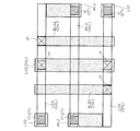
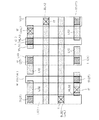
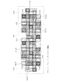
図1〜図4はこの発明の実施の形態1であるSRAMのメモリセル構造を示す図である。図1は全層におけるレイアウト構成を平面視した説明図である。図2は主として図1の第1アルミ配線層下のレイアウト構成を平面視した説明図である。図3は主として図1の第2アルミ配線層上のレイアウト構成を平面視した説明図である。なお、図2,図3で示した符号の一部を図1では省略している場合がある。
【0030】
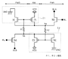
また、図4は図1〜図3で示したレイアウト構成のSRAMメモリセルの等価回路を示す回路図である。同図に示すように、実施の形態1のSRAMのメモリセルは、NMOSトランジスタN1〜N4及びPMOSトランジスタP1,P2から構成される。
【0031】
ドライバトランジスタであるPMOSトランジスタP1,P2はNウエル領域NW内に形成され、ドライバトランジスタであるNMOSトランジスタN1とアクセストランジスタであるNMOSトランジスタN4とはPウエル領域PW0内に形成され、ドライバトランジスタであるNMOSトランジスタN2とアクセストランジスタであるNMOSトランジスタN3とはPウエル領域PW1内に形成される。Pウエル領域PW0とPウエル領域PW1とはNウエル領域NWを挟んで各々反対側に形成される。
【0032】
NMOSトランジスタN1及びPMOSトランジスタP1により第1のCMOSインバータI1を構成する。すなわち、PMOSトランジスタP1及びNMOSトランジスタN1のゲートは共通に記憶端子Nbに接続され、ドレインは共通に記憶端子Naに接続される。そして、PMOSトランジスタP1のソースは電源電圧Vddに接続され、NMOSトランジスタN1のソースは接地(GND)される。
【0033】
NMOSトランジスタN2及びPMOSトランジスタP2により第2のCMOSインバータI2を構成する。すなわち、PMOSトランジスタP2及びNMOSトランジスタN2のゲートは共通に記憶端子Naに接続され、ドレインは共通に記憶端子Nbに接続される。そして、PMOSトランジスタP2のソースは電源電圧Vddに接続され、NMOSトランジスタN2のソースは接地される。
【0034】
このように、インバータI1の出力部及びインバータI2の入力部が記憶端子Naに電気的に接続され、インバータI1の入力部及びインバータI2の出力部が記憶端子Nbに電気的に接続されることにより、CMOSインバータI1,I2が互いに交叉接続され、記憶端子Na及び記憶端子Nbに互いに反転した論理レベルの情報を記憶することができる。
【0035】
NMOSトランジスタN3はビット線BLA,記憶端子Na間に介挿され、ゲートがワード線WLに接続される。NMOSトランジスタN4はビット線BLB,記憶端子Nb間に介挿されゲートがワード線WLに接続される。
【0036】
このような構成において、ビット線BLAあるいはビット線BLBより得られるデータを、ワード線WLを活性状態にして、NMOSトランジスタN3,N4をオン状態させることにより、記憶端子Na及び記憶端子Nbに対するアクセス(読み出しあるいは書き込み)が可能となる。
【0037】
以下、図1〜図3を参照して、実施の形態1のメモリセル構造について述べる。
【0038】
Nウエル領域NW内において、P+拡散領域FL110,FL111及びポリシリコン配線PL1によりPMOSトランジスタP1を構成し、P+拡散領域FL120,FL121及びポリシリコン配線PL2によりPMOSトランジスタP2を構成する。
【0039】
Pウエル領域PW0内において、N+拡散領域FL210,FL211及びポリシリコン配線PL1によりNMOSトランジスタN1を構成し、N+拡散領域FL240,FL241及びポリシリコン配線PL4によってNMOSトランジスタN4を構成する。なお、ポリシリコン配線PL1はNウエル領域NWからPウエル領域PW0にかけて形成されることにより、NMOSトランジスタN1及びPMOSトランジスタP1のゲートとして共有される。
【0040】
Pウエル領域PW1内において、N+拡散領域FL220,FL221及びポリシリコン配線PL2によりNMOSトランジスタN2を構成し、N+拡散領域FL230,FL231及びポリシリコン配線PL3によってNMOSトランジスタN3を構成する。なお、ポリシリコン配線PL2はNウエル領域NWからPウエル領域PW1にかけて形成されることにより、NMOSトランジスタN2及びPMOSトランジスタP2のゲートとして共有される。
【0041】
上記した拡散領域FL110,FL111,FL120,FL121,FL210,FL211,FL220,FL221,FL230,FL231,FL240,FL241は不純物を注入,拡散することにより得られる。
【0042】
拡散領域FL210上のグランド配線LG1(第1層アルミ配線)は拡散コンタクトホール1Cを介して拡散領域FL210と電気的に接続され、拡散領域FL211上から拡散領域FL111上及び拡散領域FL231上に伸びて形成される第1層アルミ配線であるアルミ配線AL11は、各拡散領域FL211,FL111,及びFL231それぞれと拡散コンタクトホール1Cを介して電気的に接続される。さらに、アルミ配線AL11はポリシリコン配線PL2の一部上にも形成されており、ゲートコンタクトホールGCを介してポリシリコン配線PL2に電気的に接続される。このアルミ配線AL11は電気的に低インピーダンスな接続が可能であり、記憶端子Naに相当する。
【0043】
なお、拡散コンタクトホール1Cは拡散領域と第1層(アルミ)配線とのコンタクトホールを意味し、ゲートコンタクトホールGCはポリシリコン配線と第1層配線とのコンタクトホールを意味する。
【0044】
ポリシリコン配線PL4はゲートコンタクトホールGCを介して、ワード線WL1(第1層アルミ配線)に電気的に接続され、拡散領域FL241上のビット線BLB1(第1層アルミ配線)は拡散コンタクトホール1Cを介して拡散領域FL241と電気的に接続される。
【0045】
拡散領域FL240上から拡散領域FL120上及び拡散領域FL220上に伸びて形成される第1層アルミ配線であるアルミ配線AL12は、各拡散領域FL240,FL120,及びFL220それぞれと拡散コンタクトホール1Cを介して電気的に接続される。さらに、アルミ配線AL12はポリシリコン配線PL1の一部上にも形成されており、ゲートコンタクトホールGCを介してポリシリコン配線PL1に電気的に接続される。このアルミ配線AL12は電気的に低インピーダンスな接続が可能であり、記憶端子Nbに相当する。
【0046】
拡散領域FL110上の電源配線LV1(第1層アルミ配線)は拡散コンタクトホール1Cを介して拡散領域FL110と電気的に接続され、拡散領域FL121上の電源配線LV1は拡散コンタクトホール1Cを介して拡散領域FL121と電気的に接続される。
【0047】
拡散領域FL230上のビット線BLA1(第1層アルミ配線)は拡散コンタクトホール1Cを介して拡散領域FL230と電気的に接続され、ポリシリコン配線PL3上のワード線WL1はゲートコンタクトホールGCを介してポリシリコン配線PL3と電気的に接続される。拡散領域FL221上のグランド配線LG1は拡散コンタクトホール1Cを介して拡散領域FL221と電気的に接続される。
【0048】
グランド配線LG1はビアホール1Tを介してグランド配線LG2(第2層アルミ配線(2AL))と電気的に接続され、グランド配線LG2はビアホール2Tを介してグランド配線LG3(第3層アルミ配線(3AL))と電気的に接続される。
【0049】
ワード線WL1はビアホール1Tを介してワード線WL2(第2層アルミ配線)と電気的に接続され、ワード線WL2はビアホール2Tを介してワード線WL3(第3層アルミ配線)と電気的に接続される。これらワード線WL1〜ワード線WL3によって図4のワード線WLを構成する。
【0050】
なお、ビアホール1Tは第1層配線,第2層(アルミ)配線間の接続用、ビアホール2Tは第2層配線,第3層(アルミ)配線間の接続用のビアホールを意味する。
【0051】
ワード線WL3及びグランド配線LG3はPウエル領域PW0,PW1及びNウエル領域NWを横断して互いに並行に形成され、グランド配線LG3はワード線WL3を挟んで2本形成される。
【0052】
ビット線BLA2(第2層アルミ配線)はビアホール1Tを介してビット線BLA1(図3では図示せず)と電気的に接続され、ビット線BLB2(第2層アルミ配線)はビアホール1Tを介してビット線BLB1(図3では図示せず)と電気的に接続される。電源配線LV2(第2層アルミ配線)はビアホール1Tを介して電源配線LV1(図3では図示せず)と電気的に接続される。これらビット線BLA1,BLA2及びBLB1,BLB2によってそれぞれ図4のビット線BLA及びBLBを構成する。
【0053】
ビット線BLA2,BLB2及び電源配線LV2は、それぞれPウエル領域PW1,PW0及びNウエル領域NW上を図中縦方向に互いに並行して形成される。
【0054】
このように、実施の形態1のSRAMのメモリセル構造は、NMOSトランジスタN1、N4を一方のPウエル領域PW0内に形成し、NMOSトランジスタN2、N3をNウエル領域NWを挟んだ他方のPウエル領域PW1内に形成することにより、記憶端子Naに電気的に接続されるN+拡散領域FL211及びN+拡散領域FL231をそれぞれ異なるPウエル領域PW0及びPW1内に分けて形成するとともに、記憶端子Nbに電気的に接続されるN+拡散領域FL240及びN+拡散領域FL220をそれぞれ異なるPウエル領域PW0及びPW1内に分けて形成することができる。
【0055】
その結果、α線や中性子線によって発生した電子が、Pウエル領域PW0,PW1のうち一方のPウエル領域に形成したN+拡散領域に収集された場合に、Nウエル領域NWが介在することにより上記電子の発生による影響が防止される他方のPウエル領域に形成したN+拡散領域から放出される。例えば、Pウエル領域PW0の拡散領域FL211に収集された電子は記憶端子Naを介してPウエル領域PW1の拡散領域FL231から放出され、Pウエル領域PW1の拡散領域FL220に収集された電子は記憶端子Nbを介してPウエル領域PW0の拡散領域FL240から放出される。
【0056】
このような動作により、記憶端子Na,Nbの保持データを反転させようとする電子の発生が相殺されるため、データの反転が起こりにくくなる。つまり、ソフトエラー耐性が向上するという効果がある(第1の効果)。
【0057】
また、Pウエル領域PW0とPウエル領域PW1とをビット線BLA,BLBの形成方向に垂直な方向で分離形成することより、2つのPウエル領域PW0,PW1の形成がビット線BLA,BLBの配線長に何ら影響を与えない。したがって、Pウエル領域PW0,PW1の形成によってビット線の配線長が長くなることはなく、良好なアクセスタイムを維持することができる(第2の効果)。
【0058】
また、NMOSトランジスタN1,N2及びNMOSトランジスタN3,N4はそれぞれメモリセルの中心部(Nウエル領域NWの中心部)に対して点対称となるようにレイアウト配置されるため、実施の形態1のメモリセルを複数個隣接して形成する場合に集積度の向上を図ることができる(第3の効果)。
【0059】
また、ポリシリコン配線PL1〜PL4を同一方向(図中横方向)で形成することにより、ゲート寸法の制御が容易になる効果があり、さらに、ポリシリコン配線PL1,PL3(NMOSトランジスタN1,N3、PMOSトランジスタP1)、ポリシリコン配線PL2,PL4(NMOSトランジスタN2,N4、PMOSトランジスタP2)をそれぞれ一直線上に形成することにより、無駄領域がなくなり、回路面積の削減により集積度の向上を図ることができる(第4の効果)。
【0060】
加えて、NMOSトランジスタN1〜N4において、ドレインとなる領域(記憶端子Naあるいは記憶端子Nbに電気的に接続される領域)を独立して形成することにより、ソフトエラー耐性の高いレベルで維持することができる(第5の効果)。
【0061】
さらに、CMOS構造のインバータI1,I2をそれぞれNMOSトランジスタ及びPMOSトランジスタ一つずつの組で構成することにより、CMOS構造として必要最小限の回路構成でメモリセルを実現することができる(第6の効果)。
【0062】
<実施の形態2>
図5及び図6はこの発明の実施の形態2であるSRAMのメモリセル構造を示す図である。図5は全層におけるレイアウト構成を平面視した説明図である。図6は主として図5の第1アルミ配線層下のレイアウト構成を平面視した説明図である。なお、主として図5の第2アルミ配線層上のレイアウト構成を平面視した説明図は実施の形態1の説明で用いた図3と同様であり、実施の形態2の等価回路を示す回路図は図4と同様である。また、図6,図3で示した符号の一部を図5では省略している場合がある。
【0063】
これらの図に示すように、NMOSトランジスタN1用の四角形状のN+拡散領域上に、ポリシリコン配線PL1を上記N+拡散領域の中心部で折れ曲げて形成することより、ポリシリコン配線PL1の外側に比較的広い拡散領域FL212、内側に比較的狭い拡散領域FL213を形成している。そして、拡散領域FL212,FL213及びポリシリコン配線PL1によってNMOSトランジスタN1を構成している。
【0064】
同様にして、NMOSトランジスタN2用の四角形状のN+拡散領域上に、ポリシリコン配線PL2を上記N+拡散領域の中心部で折れ曲げて形成することより、ポリシリコン配線PL2の外側に比較的広い拡散領域FL213、内側に比較的狭い拡散領域FL222を形成している。そして、拡散領域FL222,FL223及びポリシリコン配線PL2によってNMOSトランジスタN2を構成している。
【0065】
拡散領域FL212上のグランド配線LG1は2箇所の拡散コンタクトホール1Cを介して拡散領域FL212と電気的に接続され、拡散領域FL213上のアルミ配線AL11は拡散コンタクトホール1Cを介して拡散領域FL213と電気的に接続される。
【0066】
同様にして、拡散領域FL223上のグランド配線LG1は2箇所の拡散コンタクトホール1Cを介して拡散領域FL223と電気的に接続され、拡散領域FL222上のアルミ配線AL12は拡散コンタクトホール1Cを介して拡散領域FL222と電気的に接続される。他のレイアウト構成は実施の形態1と同様であるため、説明を省略する。
【0067】
実施の形態2は以上のようにレイアウト構成することにより、実施の形態1の第1,第2,第5及び第6の効果に加え以下の効果を奏する。
【0068】
ドライバトランジスタであるNMOSトランジスタN1、N2のゲート幅(チャネル幅)Wを大きくできる。その結果、ビット線BLA,BLBのキャリアの引き抜きを速く行うことにより動作の高速化が図れる。
【0069】
加えて、ドライバトランジスタであるNMOSトランジスタN1,N2のアクセストランジスタであるNMOSトランジスタN3、N4に対するゲート幅Wの比を大きくとれるのでメモリセルの安定性も向上する。
【0070】
図7は隣接するセル間のレイアウト構成を平面した説明図である。なお、図7は図6と同様、主として図5の第1アルミ配線層下のレイアウト構成を示している。
【0071】
図7ではメモリセルMC1のNウエル領域NW及びPウエル領域PW0と、メモリセルMC2のNウエル領域NW及びPウエル領域PW0とを示している。
【0072】
この際、NMOSトランジスタN1,N2はそれぞれメモリセルの中心部(Nウエル領域NWの中心部)に対して点対称となるようにレイアウト配置されている(実施の形態1の第3の効果に相当)。このため、図7に示すように、隣接するメモリセルMC1,MC2間においてドライバトランジスタであるNMOSトランジスタN1(N2)同士を、拡散領域FL212、ワード線WL1、グランド配線LG1、拡散コンタクトホール1C及びゲートコンタクトホールGCそれぞれの少なくとも一部を共有させることにより集積度を向上させながら、互いに隣接して線対称に形成することができ、NMOSトランジスタN1及びN2のゲート幅Wを大きくすることができる。
【0073】
このように、NMOSトランジスタN1,N2のゲートとなるポリシリコン配線PL1,PL2を曲げて形成したことによる面積の増加はほとんどなく、実施の形態1と同等な高密度なメモリセル構造を得ることができる。
【0074】
また、NMOSトランジスタN1,N3、PMOSトランジスタP1、及びNMOSトランジスタN2,N4、PMOSトランジスタP2をそれぞれほぼ一直線上に形成することにより、集積度の向上を図ることができる(実施の形態1の第4の効果に相当)。
【0075】
<実施の形態3>
図8〜図10はこの発明の実施の形態3であるSRAMのメモリセル構造を示す図である。図8は全層におけるレイアウト構成を平面視した説明図である。図9は主として図8の第1アルミ配線層下のレイアウト構成を平面視した説明図である。なお、主として図8の第2アルミ配線層上のレイアウト構成を平面視した説明図は実施の形態1の説明で用いた図3と同様であり、図9,図3で示した符号の一部を図8では省略している場合がある。
【0076】
図10は図8,図9,図3で示したレイアウト構成のSRAMメモリセルの等価回路を示す回路図である。同図に示すように、NMOSトランジスタN1及びPMOSトランジスタP1のゲートと記憶端子Nbとの間に抵抗R1が介挿され、NMOSトランジスタN2及びPMOSトランジスタP2のゲートと記憶端子Naとの間に抵抗R2が介挿される。他の構成は図4で示した実施の形態1と同様であるため説明を省略する。
【0077】
以下、図8,図9及び図3を参照して、実施の形態3のメモリセル構造について述べる。
【0078】
これらの図に示すように、NMOSトランジスタN1及びPMOSトランジスタP1のゲートとなるポリシリコン配線PL13(実施の形態1のポリシリコン配線PL1に相当)が抵抗R1となる高抵抗金属配線M00に電気的に接続され、この高抵抗金属配線M00がビアホール0Tを介して記憶端子Nbであるアルミ配線AL12と電気的に接続される。ビアホール0Tはポリシリコン配線と同一層に形成された高抵抗金属配線M00と第1層配線との接続用のビアホールを意味する。
【0079】
同様にして、NMOSトランジスタN2及びPMOSトランジスタP2のゲートとなるポリシリコン配線PL14(実施の形態1のポリシリコン配線PL2に相当)が抵抗R2となる高抵抗金属配線M01に電気的に接続され、この高抵抗金属配線M01がビアホール0Tを介して記憶端子Naであるアルミ配線AL11と電気的に接続される。
【0080】
なお、高抵抗金属配線M00,M01の形成材料としては例えばタングステン等のCoSi2(コバルトシリサイド)より抵抗率が高い材料が挙げられる。また、他の構成は図1〜図3で示した実施の形態1と同様であるため、説明を省略する。
【0081】
実施の形態3は上記のようなメモリセル構造を有することにより、実施の形態1の第1〜第6の効果に加え、以下の効果を奏する。
【0082】
実施の形態3のメモリセルは、抵抗R1,R2を伝播する信号遅延によってセルに保持しているデータを反転するための応答特性は長くなる。その結果、α線や中性子線によって発生した電子によって、記憶端子Na,Nbのうち一方の記憶端子の電位が反転したとしても、他方の記憶端子のデータが反転する以前に元の保持状態に戻るため、ソフトエラーはより起きにくくなる。
【0083】
<実施の形態4>
図11及び図12はこの発明の実施の形態4であるSRAMのメモリセル構造を示す図である。図11は全層におけるレイアウト構成を平面視した説明図である。図12は主として図11の第1アルミ配線層下のレイアウト構成を平面視した説明図である。なお、主として図11の第2アルミ配線層上のレイアウト構成を平面視した説明図は実施の形態1の説明で用いた図3と同様であり、図12,図3で示した符号の一部を図11では省略している場合がある。また、実施の形態4のレイアウト構成のSRAMメモリセルの等価回路は実施の形態3で示した図10と同様である。
【0084】
以下、図11,図12及び図3を参照して、実施の形態4のメモリセル構造について述べる。
【0085】
これらの図に示すように、NMOSトランジスタN1及びPMOSトランジスタP1のゲートとなるポリシリコン配線PL13,PL17(実施の形態1のポリシリコン配線PL1に相当)のうち、抵抗R1となるポリシリコン配線PL17はポリシリコン配線PL13に比べ高抵抗な材料で形成される。例えば、ポリシリコン配線PL13をCoSi2で形成した場合、ポリシリコン配線PL17をCoSi2より抵抗率が高い形成材料を用いて形成する。
【0086】
そして、ポリシリコン配線PL17がゲートコンタクトホールGCを介して記憶端子Nbであるアルミ配線AL12と電気的に接続される。
【0087】
同様にして、NMOSトランジスタN2及びPMOSトランジスタP2のゲートとなるポリシリコン配線PL14,PL18(実施の形態1のポリシリコン配線PL2に相当)のうち、抵抗R2となるポリシリコン配線PL18はポリシリコン配線PL14に比べ高抵抗な材料で形成され、ポリシリコン配線PL18がゲートコンタクトホールGCを介して記憶端子Naであるアルミ配線AL11と電気的に接続される。他の構成は図1〜図3で示した実施の形態1と同様であるため、説明を省略する。
【0088】
実施の形態4は上記のようなメモリセル構造を有することにより、実施の形態1の第1〜第6の効果に加え、以下の効果を奏する。
【0089】
実施の形態4のメモリセルは、抵抗R1,R2を伝播する信号遅延によってセルに保持しているデータを反転するための応答特性は長くなる。その結果、α線や中性子線によって発生した電子によって、記憶端子Na,Nbのうち一方の記憶端子の電位が反転したとしても、他方の記憶端子のデータが反転する以前に元の保持状態に戻るため、ソフトエラーはより起きにくくなる。
【0090】
<実施の形態5>
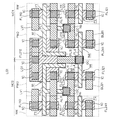
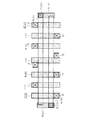
図13〜図15はこの発明の実施の形態5であるSRAMのメモリセル構造を示す図である。図13は全層におけるレイアウト構成を平面視した説明図である。図14は主として図13の第2アルミ配線層上のレイアウト構成を平面視した説明図である。なお、主として図13の第1アルミ配線層下のレイアウト構成を平面視した説明図は実施の形態1の説明で用いた図2(ワード線WL2がワード線WLA2,WLB2に分離された点は異なる)と同様であり、図14,図2で示した符号の一部を図13では省略している場合がある。
【0091】
図15は図13,図14,図2で示したレイアウト構成のSRAMメモリセルの等価回路を示す回路図である。同図に示すように、NMOSトランジスタN3のゲートにはワード線WLAが接続され、NMOSトランジスタN4のゲートにはワード線WLAとは独立したワード線WLBが接続される。なお、他の構成は図4で示した実施の形態1と同様であるため説明を省略する。
【0092】
以下、図13,図14及び図2を参照して、実施の形態5のメモリセル構造について述べる。
【0093】
ポリシリコン配線PL3はゲートコンタクトホールGCを介して、ワード線WLA1(第1層アルミ配線)に電気的に接続され、ワード線WLA1はビアホール1Tを介してワード線WLA2(第2層アルミ配線)と電気的に接続され、ワード線WLA2はビアホール2Tを介してワード線WLA3(第3層アルミ配線)と電気的に接続される。これらのワード線WLA1〜ワード線WLA3によって図15のワード線WLAを構成する。
【0094】
同様にして、ポリシリコン配線PL4はゲートコンタクトホールGCを介して、ワード線WLB1(第1層アルミ配線)に電気的に接続され、ワード線WLB1はビアホール1Tを介してワード線WLB2(第2層アルミ配線)と電気的に接続され、ワード線WLB2はビアホール2Tを介してワード線WLB3(第3層アルミ配線)と電気的に接続される。これらワード線WLB1〜WLB3によって図15のワード線WLBを構成する。
【0095】
ワード線WLA3,WLB3及びグランド配線LG3はPウエル領域PW0,PW1及びNウエル領域NWを横断して互いに並行に形成され、グランド配線LG3はワード線WLA3,WLB3を挟んで2本形成される。なお、他のレイアウト構成は実施の形態1と同様であるため説明を省略する。
【0096】
実施の形態5は上記のようなメモリセル構造を有することにより、実施の形態1の第1〜第6の効果に加え、以下の効果を奏する。
【0097】
図15の等価回路に示すように、アクセストランジスタであるNMOSトランジスタN3、N4のゲートに接続するワード線をWLA、WLBと分けることで、FIFOメモリで利用可能なメモリセル構造を実現することができる。
【0098】
<実施の形態6>
図16〜図18はこの発明の実施の形態6であるSRAMのメモリセル構造を示す図である。図16は全層におけるレイアウト構成を平面視した説明図である。図17は主として図16の第1アルミ配線層下のレイアウト構成を平面視した説明図である。図18は主として図16の第2アルミ配線層上のレイアウト構成を平面視した説明図である。なお、図17,図18で示した符号の一部を図16では省略している場合がある。また、実施の形態6のレイアウト構成のSRAMメモリセルの等価回路は実施の形態5で示した図15と同様である。
【0099】
以下、図16〜図18を参照して、実施の形態6のメモリセル構造について述べる。
【0100】
NMOSトランジスタN3、N4用のN+拡散領域はソース・ドレイン領域形成方向が、他のNMOSトランジスタN1,N2及びPMOSトランジスタP1,P2のソース・ドレイン領域形成方向と90度向きを変えて形成される。すなわち、NMOSトランジスタN3用の拡散領域FL242,FL243とNMOSトランジスタN4用の拡散領域FL232,FL233とが図中、横方向に形成される。
【0101】
そして、拡散領域FL243上のビット線BLB1は拡散コンタクトホール1Cを介して拡散領域FL243に電気的に接続され、ビット線BLB2(第2層アルミ配線)はビアホール1Tを介してビット線BLB1(図18では図示せず)に電気的に接続される。
【0102】
同様にして、NMOSトランジスタN3を構成する拡散領域FL232上のビット線BLA1は拡散コンタクトホール1Cを介して拡散領域FL232に電気的に接続され、ビット線BLA2(第2層アルミ配線)はビアホール1Tをビット線BLA1(図18では図示せず)に電気的に接続される。
【0103】
ビット線BLA2,BLB2はPウエル領域PW0,PW1及びNウエル領域NWを横断して互いに並行に形成される。
【0104】
グランド配線LG1は拡散コンタクトホール1Cを介して拡散領域FL210及び拡散領域FL221に電気的に接続され、グランド配線LG2はビアホール1Tを介してグランド配線LG1(図18では図示せず)に電気的に接続され、グランド配線LG3はビアホール2Tを介してグランド配線LG2と電気的に接続される。
【0105】
電源配線LV1は拡散コンタクトホール1Cを介して拡散領域FL110及びFL121に電気的に接続され、電源配線LV2はビアホール1Tを介して電源配線LV1(図18では図示せず)に電気的に接続され、電源配線LV3はビアホール2Tを介して電源配線LV2に電気的に接続される。
【0106】
ワード線WLA1はゲートコンタクトホールGCを介してポリシリコン配線PL23に電気的に接続され、ワード線WLA2はビアホール1Tを介してワード線WLA1(図18では図示せず)に電気的に接続され、ワード線WLA3(第3層アルミ配線)はビアホール2Tを介してワード線WLA2に電気的に接続される。
【0107】
同様にして、ワード線WLB1はゲートコンタクトホールGCを介してポリシリコン配線PL24に電気的に接続され、ワード線WLB2はビアホール1Tを介してワード線WLB1(図18では図示せず)に電気的に接続され、ワード線WLB3(第3層アルミ配線)はビアホール2Tを介してワード線WLB2に電気的に接続される。
【0108】
(第1の)グランド配線LG3、ワード線WLB3、電源配線LV3、ワード線WLA3、(第2の)グランド配線LG3はそれぞれ図中縦方向に並列に形成され、(第1の)グランド配線LG3及びワード線WLB3はPウエル領域PW0上に、電源配線LV3はNウエル領域NW上に、ワード線WLA3及び(第2の)グランド配線LG3はPウエル領域PW1上に形成される。
【0109】
実施の形態6は上記のようなメモリセル構造を有することにより、実施の形態1の第1〜第3,第5及び第6の効果に加え、実施の形態5固有の効果と同等の効果を奏する。
【0110】
<実施の形態7>
図19〜図21はこの発明の実施の形態7であるSRAMのメモリセル構造を示す図である。図19は全層におけるレイアウト構成を平面視した説明図である。図20は主として図19の第1アルミ配線層下のレイアウト構成を平面視した説明図である。図21は主として図19の第2アルミ配線層上のレイアウト構成を平面視した説明図である。なお、図20,図21で示した符号の一部を図19では省略している場合がある。また、実施の形態7のレイアウト構成のSRAMメモリセルの等価回路は実施の形態1で示した図4と同様である。
【0111】
以下、図19〜図21を参照して、実施の形態7のメモリセル構造について述べる。
【0112】
NMOSトランジスタN3,N4の共用ポリシリコン配線PL5がPウエル領域PW0からNウエル領域NW及びPウエル領域PW1上に伸びて形成され、この共用ポリシリコン配線PL5が図4のワード線WLとして用いられる。
【0113】
他の構成は、ポリシリコン配線PL1,PL2のパターン形状、ポリシリコン配線PL1とアルミ配線AL12とのゲートコンタクトホールGC形成位置及びポリシリコン配線PL2とアルミ配線AL11とのゲートコンタクトホールGCの形成位置等を除き、図5,図6及び図3で示した実施の形態2と同様である。
【0114】
実施の形態7は上記のようなメモリセル構造を有することにより、実施の形態2と同等の効果を奏する。さらに、ワード線WLに関して、ビアホール1T,2T及びワード線WL2,WL3が不要になるため、必要レイア数が減り、コスト削減が図れるという効果がある。
【0115】
<実施の形態8>
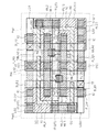
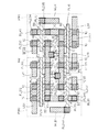
図22〜図25はこの発明の実施の形態8であるSRAMのメモリセル構造を示す図である。図22は全層におけるレイアウト構成を平面視した説明図である。図23は主として図22の第1アルミ配線層下のレイアウト構成を平面視した説明図である。図24は主として図22の第2アルミ配線層上のレイアウト構成を平面視した説明図である。なお、図23,図24で示した符号の一部を図22では省略している場合がある。
【0116】
また、図25は図22〜図24で示したレイアウト構成のSRAMメモリセルの等価回路を示す回路図である。同図に示すように、実施の形態8のSRAMのメモリセルは、NMOSトランジスタN1,N2,N5〜N8及びPMOSトランジスタP1,P2から構成される。
【0117】
NMOSトランジスタN5はビット線BLA,記憶端子Nb間に介挿され、NMOSトランジスタN6はビット線バーBLA,記憶端子Na間に介挿され、NMOSトランジスタN5及びN6のゲートがワード線WLAに共通に接続される。
【0118】
NMOSトランジスタN7はビット線BLB,記憶端子Na間に介挿され、NMOSトランジスタN8はビット線バーBLB,記憶端子Nb間に介挿され、NMOSトランジスタN7及びN8のゲートがワード線WLBに共通に接続される。
【0119】
ドライバトランジスタであるPMOSトランジスタP1,P2はNウエル領域NW内に形成され、ドライバトランジスタであるNMOSトランジスタN1とアクセストランジスタであるNMOSトランジスタN7,N8とはPウエル領域PW0内に形成され、ドライバトランジスタであるNMOSトランジスタN2とアクセストランジスタであるNMOSトランジスタN5,N6とはPウエル領域PW1内に形成される。Pウエル領域PW0とPウエル領域PW1とはNウエル領域NWを挟んで各々反対側に形成される。なお、他の構成は図15で示した実施の形態5の等価回路と同様である。
【0120】
以下、図22〜図24を参照して、実施の形態8のメモリセル構造について述べる。
【0121】
Nウエル領域NW内において、P+拡散領域FL110,FL111及びポリシリコン配線PL17によりPMOSトランジスタP1を構成し、P+拡散領域FL120,FL121及びポリシリコン配線PL18によりPMOSトランジスタP2を構成する。
【0122】
Pウエル領域PW0内において、N+拡散領域FL212,FL213及びポリシリコン配線PL17によりNMOSトランジスタN1を構成し、N+拡散領域FL244,FL245及びポリシリコン配線PL20によってNMOSトランジスタN7を構成し、N+拡散領域FL246,FL247及びポリシリコン配線PL20によってNMOSトランジスタN8を構成する。なお、ポリシリコン配線PL17はNウエル領域NWからPウエル領域PW0にかけて形成されることにより、NMOSトランジスタN1及びPMOSトランジスタP1のゲートとして共有され、ポリシリコン配線PL20はNMOSトランジスタN7,N8間で共有される。
【0123】
Pウエル領域PW1内において、N+拡散領域FL222,FL223及びポリシリコン配線PL18によりNMOSトランジスタN2を構成し、N+拡散領域FL234,FL235及びポリシリコン配線PL19によってNMOSトランジスタN5を構成し、N+拡散領域FL236,FL237及びポリシリコン配線PL19によってNMOSトランジスタN3を構成する。なお、ポリシリコン配線PL18はNウエル領域NWからPウエル領域PW1にかけて形成されることにより、NMOSトランジスタN2及びPMOSトランジスタP2のゲートとして共有され、ポリシリコン配線PL18はNMOSトランジスタN5,N6間で共有される。なお、上記した拡散領域は不純物を注入,拡散することにより得られる。
【0124】
拡散領域FL212上のグランド配線LG1は2つの拡散コンタクトホール1Cを介して拡散領域FL212に電気的に接続され、拡散領域FL245上のビット線BLB1は拡散コンタクトホール1Cを介して拡散領域FL245に電気的に接続され、拡散領域FL247上のビット線バーBLB1は拡散コンタクトホール1Cを介して拡散領域FL247に電気的に接続される。
【0125】
拡散領域FL244上から、拡散領域FL213上、拡散領域FL111上及び拡散領域FL237上に伸びて形成される第1層アルミ配線であるアルミ配線AL15は、各拡散領域FL244,FL213,FL111,及びFL237それぞれと拡散コンタクトホール1Cを介して電気的に接続される。さらに、アルミ配線AL15はポリシリコン配線PL18の一部上にも形成されており、ゲートコンタクトホールGCを介してポリシリコン配線PL18に電気的に接続される。このアルミ配線AL15は電気的に低インピーダンスな接続が可能であり、記憶端子Naに相当する。
【0126】
ポリシリコン配線PL20はゲートコンタクトホールGCを介して、ワード線WLB1に電気的に接続される。
【0127】
拡散領域FL110上の電源配線LV1は拡散コンタクトホール1Cを介して拡散領域FL110と電気的に接続され、拡散領域FL121上の電源配線LV1は拡散コンタクトホール1Cを介して拡散領域FL121と電気的に接続される。
【0128】
グランド配線LG1は2つの拡散コンタクトホール1Cを介して拡散領域FL223に電気的に接続され、拡散領域FL234上のビット線BLA1は拡散コンタクトホール1Cを介して拡散領域FL234に電気的に接続され、拡散領域FL236上のビット線バーBLA1は拡散コンタクトホール1Cを介して拡散領域FL236と電気的に接続される。
【0129】
拡散領域FL235上から、拡散領域FL222上、拡散領域FL120上及び拡散領域FL246上に伸びて形成される第1層アルミ配線であるアルミ配線AL16は、各拡散領域FL235,FL222,FL120,及びFL246それぞれと拡散コンタクトホール1Cを介して電気的に接続される。さらに、アルミ配線AL16はポリシリコン配線PL17の一部上にも形成されており、ゲートコンタクトホールGCを介してポリシリコン配線PL17に電気的に接続される。このアルミ配線AL16は電気的に低インピーダンスな接続が可能であり、記憶端子Nbに相当する。
【0130】
ポリシリコン配線PL19上のワード線WLA1はゲートコンタクトホールGCを介してポリシリコン配線PL19と電気的に接続される。
【0131】
グランド配線LG1はビアホール1Tを介してグランド配線LG2に電気的に接続され、グランド配線LG2はビアホール2Tを介してグランド配線LG3に電気的に接続される。
【0132】
ワード線WLA1はビアホール1Tを介してワード線WLA2に電気的に接続され、ワード線WLA2はビアホール2Tを介してワード線WLA3に電気的に接続される。これらワード線WLA1〜ワード線WLA3によって図25のワード線WLAを構成する。
【0133】
同様にして、ワード線WLB1はビアホール1Tを介してワード線WLB2に電気的に接続され、ワード線WLB2はビアホール2Tを介してワード線WLB3に電気的に接続される。これらワード線WLB1〜ワード線WLB3によって図25のワード線WLBを構成する。
【0134】
ワード線WLA3,WLB3及びグランド配線LG3はPウエル領域PW0,PW1及びNウエル領域NWを横断して互いに並行に形成され、グランド配線LG3はワード線WLA3,WLB3を挟んで2本形成される。
【0135】
ビット線BLA2はビアホール1Tを介してビット線BLA1に電気的に接続され、ビット線BLB2はビアホール1Tを介してビット線BLB1に電気的に接続される。
【0136】
同様にして、ビット線バーBLA2はビアホール1Tを介してビット線バーBLA1に電気的に接続され、ビット線バーBLB2はビアホール1Tを介してビット線バーBLB1に電気的に接続される。
【0137】
電源配線LV2はビアホール1Tを介して電源配線LV1に電気的に接続される。これらビット線BLA1,BLA2、バーBLA1,バーBLA2、BLB1,BLB2、及びバーBLB1,BLB2によってそれぞれ図25のビット線BLA,バーBLA、BLB及びバーBLBを構成する。
【0138】
ビット線対BLA2,バーBLA2、ビット線対BLB2,バーBLB2及び電源配線LV2は、それぞれPウエル領域PW1,PW0及びNウエル領域NW上を図中縦方向に互いに並行して形成される。
【0139】
このように、実施の形態8のSRAMのメモリセル構造は、NMOSトランジスタN1、N7,N8を一方のPウエル領域PW0内に形成し、NMOSトランジスタN2、N5,N6をNウエル領域NWを挟んだ他方のPウエル領域PW1内に形成することにより、記憶端子Naに電気的に接続されるN+拡散領域FL213及びFL244とN+拡散領域FL237とをそれぞれ異なるPウエル領域PW0内とPW1内とに分けて形成するとともに、記憶端子Nbに電気的に接続されるN+拡散領域FL222及びFL235とN+拡散領域FL246とをそれぞれ異なるPウエル領域PW1内とPW0内とに分けて形成すことができる。
【0140】
その結果、実施の形態1の第1の効果であるソフトエラー耐性が向上を図ることができる。
【0141】
また、Pウエル領域PW0及びPW1を、ビット線対BLA,バーBLA及びビット線対BLB,バーBLBの形成方向に垂直な方向で分離形成することより、2つのPウエル領域PW0,PW1の形成がビット線対BLA,バーBLA及びビット線対BLB,バーBLBの配線長に何ら影響を与えない。したがって、Pウエル領域PW0,PW1の形成によってビット線の配線長が長くなることはなく、実施の形態1の第2の効果である良好なアクセスタイムを維持することができる。
【0142】
また、NMOSトランジスタN1,N2、NMOSトランジスタN5,N7,及びNMOSトランジスタN6,N8はそれぞれメモリセルの中心部(Nウエル領域NWの中心部)に対して点対称となるようにレイアウト配置されるため、実施の形態8のメモリセルを複数個隣接して形成する場合に集積度の向上を図ることができる(実施の形態1の第3の効果に相当)。
【0143】
また、ポリシリコン配線PL17〜PL20を同一方向(図中横方向)で形成することにより、ゲート寸法の制御が容易になる効果があり、さらに、ポリシリコン配線PL17,PL19、ポリシリコン配線PL18,PL20をそれぞれ一直線上に形成することにより、無駄領域がなくなり、回路面積の削減により集積度の向上を図ることができる(実施の形態1の第4の効果に相当)。
【0144】
さらに、NMOSトランジスタN1,N2,N5〜N8において、ドレインとなる領域を独立して形成することにより、ソフトエラー耐性の高いレベルで維持することができる(実施の形態1の第5の効果に相当)。
【0145】
さらに、CMOS構造のインバータI1,I2をそれぞれNMOSトランジスタ及びPMOSトランジスタ一つずつの組で構成するここにより、CMOS構造として必要最小限の回路構成でメモリセルを実現することができる(実施の形態1の第6の効果に相当)。
【0146】
加えて、実施の形態8のメモリセルは、図25に示すように、2つのワード線WLA,WLB及び2つのビット線対(ビット線対BLA,バーBLA及びビット線対BLB,バーBLB)を用いた2ポートメモリセルが実現する。
【0147】
<実施の形態9>
図26〜図28はこの発明の実施の形態9であるSRAMのメモリセル構造を示す図である。図26は全層におけるレイアウト構成を平面視した説明図である。図27は主として図26の第1アルミ配線層下のレイアウト構成を平面視した説明図である。図28は主として図26の第2アルミ配線層上のレイアウト構成を平面視した説明図である。なお、図27,図28で示した符号の一部を図26では省略している場合がある。
【0148】
また、実施の形態9のレイアウト構成のSRAMメモリセルの等価回路は図25で示した実施の形態8と同様である。
【0149】
以下、図26〜図28を参照して、実施の形態9のメモリセル構造について、実施の形態8と異なる構成を中心に述べる。
【0150】
Pウエル領域PW0内において、N+拡散領域FL214,FL215及びポリシリコン配線PL31によりNMOSトランジスタN1を構成する。このとき、ポリシリコン配線PL31をNMOSトランジスタN1用のN+拡散領域(FL214,FL215)上において2度90度折り曲げて形成することにより、他のNMOSトランジスタN5〜N8に比べてかなり大きなゲート幅を設定している。
【0151】
N+拡散領域FL270,FL271及びポリシリコン配線PL37によってNMOSトランジスタN7を構成し、N+拡散領域FL280,FL281及びポリシリコン配線PL38によってNMOSトランジスタN8を構成する。
【0152】
なお、ポリシリコン配線PL31はNウエル領域NWからPウエル領域PW0にかけて形成されることにより、NMOSトランジスタN1及びPMOSトランジスタP1のゲートとして共有される。
【0153】
Pウエル領域PW1内において、N+拡散領域FL224,FL225及びポリシリコン配線PL32によりNMOSトランジスタN2を構成する。このとき、ポリシリコン配線PL32をNMOSトランジスタN2用のN+拡散領域(FL224,FL225)上において2度90度折り曲げて形成することにより、他のNMOSトランジスタN5〜N8に比べてかなり大きなゲート幅を設定している。
【0154】
N+拡散領域FL250,FL251及びポリシリコン配線PL35によってNMOSトランジスタN5を構成し、N+拡散領域FL260,PL261及びポリシリコン配線PL36によってNMOSトランジスタN6を構成する。
【0155】
なお、ポリシリコン配線PL32はNウエル領域NWからPウエル領域PW1にかけて形成されることにより、NMOSトランジスタN2及びPMOSトランジスタP2のゲートとして共有される。なお、上記した拡散領域は不純物を注入,拡散することにより得られる。
【0156】
拡散領域FL214上の2つのグランド配線LG1はそれぞれ拡散コンタクトホール1Cを介して拡散領域FL214に電気的に接続され、拡散領域FL271上のビット線BLB1は拡散コンタクトホール1Cを介して拡散領域FL271に電気的に接続され、拡散領域FL280上のビット線バーBLB1は拡散コンタクトホール1Cを介して拡散領域FL280に電気的に接続される。
【0157】
拡散領域FL281上から、拡散領域FL215上、拡散領域FL111上及び拡散領域FL251上に伸びて形成される第1層アルミ配線であるアルミ配線AL17は、各拡散領域FL281,FL215,FL111,及びFL251それぞれと拡散コンタクトホール1Cを介して電気的に接続される。さらに、アルミ配線AL17はポリシリコン配線PL32の一部上にも形成されており、ゲートコンタクトホールGCを介してポリシリコン配線PL32に電気的に接続される。このアルミ配線AL17は電気的に低インピーダンスな接続が可能であり、記憶端子Naに相当する。
【0158】
ポリシリコン配線PL37及びPL38はそれぞれゲートコンタクトホールGCを介して共通にワード線WLB1に電気的に接続される。
【0159】
拡散領域FL110上の電源配線LV1は拡散コンタクトホール1Cを介して拡散領域FL110に電気的に接続され、拡散領域FL121上の電源配線LV1は拡散コンタクトホール1Cを介して拡散領域FL121に電気的に接続される。
【0160】
2つのグランド配線LG1はそれぞれ拡散コンタクトホール1Cを介して拡散領域FL224に電気的に接続され、拡散領域FL250上のビット線BLA1は拡散コンタクトホール1Cを介して拡散領域FL250に電気的に接続され、拡散領域FL261上のビット線バーBLA1は拡散コンタクトホール1Cを介して拡散領域FL261と電気的に接続される。
【0161】
拡散領域FL260上から、拡散領域FL225上、拡散領域FL120上及び拡散領域FL270上に伸びて形成される第1層アルミ配線であるアルミ配線AL18は、各拡散領域FL260,FL225,FL120,及びFL270それぞれと拡散コンタクトホール1Cを介して電気的に接続される。さらに、アルミ配線AL18はポリシリコン配線PL31の一部上にも形成されており、ゲートコンタクトホールGCを介してポリシリコン配線PL31に電気的に接続される。このアルミ配線AL18は電気的に低インピーダンスな接続が可能であり、記憶端子Nbに相当する。
【0162】
ポリシリコン配線PL35及びPL36上のワード線WLA1はゲートコンタクトホールGCを介して共通にポリシリコン配線PL35及びPL36に電気的に接続される。
【0163】
グランド配線LG1はビアホール1Tを介してグランド配線LG2に電気的に接続され、グランド配線LG2はビアホール2Tを介してグランド配線LG3に電気的に接続される。
【0164】
ワード線WLA1はビアホール1Tを介してワード線WLA2に電気的に接続され、ワード線WLA2はビアホール2Tを介してワード線WLA3に電気的に接続される。同様にして、ワード線WLB1はビアホール1Tを介してワード線WLB2に電気的に接続され、ワード線WLB2はビアホール2Tを介してワード線WLB3に電気的に接続される。
【0165】
ビット線BLA2はビアホール1Tを介してビット線BLA1に電気的に接続され、ビット線BLB2はビアホール1Tを介してビット線BLB1に電気的に接続される。
【0166】
同様にして、ビット線バーBLA2はビアホール1Tを介してビット線バーBLA1に電気的に接続され、ビット線バーBLB2はビアホール1Tを介してビット線バーBLB1に電気的に接続される。また、電源配線LV2はビアホール1Tを介して電源配線LV1に電気的に接続される。
【0167】
このように、実施の形態9のSRAMのメモリセル構造は、NMOSトランジスタN1、N7,N8を一方のPウエル領域PW0内に形成し、NMOSトランジスタN2,N5,N6をNウエル領域NWを挟んだ他方のPウエル領域PW1内に形成することにより、実施の形態8と同様、実施の形態1の第1の効果であるソフトエラー耐性が向上を図ることができる。
【0168】
また、Pウエル領域PW0及びPW1を、ビット線対BLA,バーBLA及びビット線対BLB,バーBLBの形成方向に垂直な方向で分離形成することより、実施の形態1の第2の効果である良好なアクセスタイムを維持することができる。
【0169】
また、実施の形態9は、実施の形態8と同様、NMOSトランジスタN1,N2、NMOSトランジスタN5,N7,及びNMOSトランジスタN6,N8はそれぞれメモリセルの中心部に対して点対称となるようにレイアウト配置されるため、実施の形態9のメモリセルを複数個隣接して形成する場合に集積度の向上を図ることができる(実施の形態1の第3の効果に相当)。
【0170】
さらに、NMOSトランジスタN1,N2,N5〜N8において、ドレインとなる領域を独立して形成することにより、ソフトエラー耐性の高いレベルで維持することができる(実施の形態1の第5の効果に相当)。
【0171】
加えて、CMOS構造のインバータI1,I2をそれぞれNMOSトランジスタ及びPMOSトランジスタ一つずつの組で構成するここにより、CMOS構造として必要最小限の回路構成でメモリセルを実現することができる(実施の形態1の第6の効果に相当)。
【0172】
さらに、実施の形態9のメモリセルは、実施の形態8と同様、2ポートメモリセルとなる。
【0173】
さらに加えて、ドライバトランジスタであるNMOSトランジスタN1、N2のゲート幅(チャネル幅)Wを大きくすることにより、実施の形態2と同様、動作の高速化及びメモリセルの安定性の向上を図ることができる。
【0174】
<実施の形態10>
図29〜図31はこの発明の実施の形態10であるSRAMのメモリセル構造を示す図である。図29は全層におけるレイアウト構成を平面視した説明図である。図30は主として図29の第1アルミ配線層下のレイアウト構成を平面視した説明図である。図31は主として図29の第2アルミ配線層上のレイアウト構成を平面視した説明図である。なお、図30,図31で示した符号の一部を図29では省略している場合がある。
【0175】
また、実施の形態10のレイアウト構成のSRAMメモリセルの等価回路は図25で示した実施の形態8と同様である。
【0176】
以下、図29〜図31を参照して、実施の形態10のメモリセル構造について述べる。
【0177】
Nウエル領域NW内において、P+拡散領域FL110,FL111及びポリシリコン配線PL41によりPMOSトランジスタP1を構成し、P+拡散領域FL120,FL121及びポリシリコン配線PL42によりPMOSトランジスタP2を構成する。
【0178】
Pウエル領域PW0内において、N+拡散領域FL210,FL211及びポリシリコン配線PL41によりNMOSトランジスタN1を構成し、N+拡散領域FL270,FL271及びポリシリコン配線PL47によってNMOSトランジスタN7を構成し、N+拡散領域FL280,FL281及びポリシリコン配線PL47によってNMOSトランジスタN8を構成する。なお、ポリシリコン配線PL41はNウエル領域NWからPウエル領域PW0にかけて形成されることにより、NMOSトランジスタN1及びPMOSトランジスタP1のゲートとして共有され、ポリシリコン配線PL47はNMOSトランジスタN7,N8間で共有される。
【0179】
Pウエル領域PW1内において、N+拡散領域FL220,FL221及びポリシリコン配線PL42によりNMOSトランジスタN2を構成し、N+拡散領域FL250,FL251及びポリシリコン配線PL45によってNMOSトランジスタN5を構成し、N+拡散領域FL260,FL261及びポリシリコン配線PL45によってNMOSトランジスタN6を構成する。なお、ポリシリコン配線PL42はNウエル領域NWからPウエル領域PW1にかけて形成されることにより、NMOSトランジスタN2及びPMOSトランジスタP2のゲートとして共有され、ポリシリコン配線PL42はNMOSトランジスタN5,N6間で共有される。なお、上記した拡散領域は不純物を注入,拡散することにより得られる。
【0180】
拡散領域FL210上のグランド配線LG1は拡散コンタクトホール1Cを介して拡散領域FL210に電気的に接続され、拡散領域FL271上のビット線BLB1は拡散コンタクトホール1Cを介して拡散領域FL271に電気的に接続され、拡散領域FL281上のビット線バーBLB1は拡散コンタクトホール1Cを介して拡散領域FL281に電気的に接続される。
【0181】
拡散領域FL270(FL211)上から拡散領域FL111上に伸びて形成される第1層アルミ配線であるアルミ配線AL17は、拡散領域FL270(FL211)と拡散コンタクトホール1Cを介して電気的に接続される。
【0182】
さらに、アルミ配線AL17はポリシリコン配線PL42に電気的に接続される。ポリシリコン配線PL42はシェアードコンタクトSCを介して拡散領域FL111及び拡散領域FL261それぞれに電気的に接続される。なお、ここで、シェアードコンタクトは、拡散領域とポリシリコンを1つの共通コンタクトで電気的に接続するものを意味する。
【0183】
アルミ配線AL17は電気的に低インピーダンスな接続が可能であり、アルミ配線AL17、2つのシェアードコンタクトSC及びポリシリコン配線PL42が記憶端子Naに相当する。
【0184】
ポリシリコン配線PL47はゲートコンタクトホールGCを介して、ワード線WLB1に電気的に接続される。
【0185】
拡散領域FL110上の電源配線LV1は拡散コンタクトホール1Cを介して拡散領域FL110と電気的に接続され、拡散領域FL121上の電源配線LV1は拡散コンタクトホール1Cを介して拡散領域FL121に電気的に接続される。
【0186】
グランド配線LG1は拡散コンタクトホール1Cを介して拡散領域FL221に電気的に接続され、拡散領域FL250上のビット線BLA1は拡散コンタクトホール1Cを介して拡散領域FL250に電気的に接続され、拡散領域FL260上のビット線バーBLA1は拡散コンタクトホール1Cを介して拡散領域FL260と電気的に接続される。
【0187】
拡散領域FL251(FL220)上から拡散領域FL120上に伸びて形成される第1層アルミ配線であるアルミ配線AL18は、拡散領域FL251(FL220)と拡散コンタクトホール1Cを介して電気的に接続される。
【0188】
さらに、アルミ配線AL19はポリシリコン配線PL41に電気的に接続される。ポリシリコン配線PL41はシェアードコンタクトSCを介して拡散領域FL120及び拡散領域FL280それぞれに電気的に接続される。
【0189】
アルミ配線AL18は電気的に低インピーダンスな接続が可能であり、アルミ配線AL18、2つのシェアードコンタクトSC及びポリシリコン配線PL41が記憶端子Nbに相当する。
【0190】
ポリシリコン配線PL45上のワード線WLA1はゲートコンタクトホールGCを介してポリシリコン配線PL45と電気的に接続される。
【0191】
ワード線WLA1はビアホール1Tを介してワード線WLA2に電気的に接続され、ワード線WLA2はビアホール2Tを介してワード線WLA3に電気的に接続される。同様にして、ワード線WLB1はビアホール1Tを介してワード線WLB2に電気的に接続され、ワード線WLB2はビアホール2Tを介してワード線WLB3に電気的に接続される。
【0192】
ワード線WLA3及びWLB3は、Pウエル領域PW0,PW1及びNウエル領域NWを横断して互いに並行に形成される。
【0193】
ビット線BLA2はビアホール1Tを介してビット線BLA1に電気的に接続され、ビット線BLB2はビアホール1Tを介してビット線BLB1に電気的に接続される。
【0194】
同様にして、ビット線バーBLA2はビアホール1Tを介してビット線バーBLA1に電気的に接続され、ビット線バーBLB2はビアホール1Tを介してビット線バーBLB1に電気的に接続される。
【0195】
電源配線LV2はビアホール1Tを介して電源配線LV1に電気的に接続される。グランド配線LG1はビアホール1Tを介してグランド配線LG2に電気的に接続される。
【0196】
ビット線対BLA2,バーBLA2、ビット線対BLB2,バーBLB2、グランド配線LG2及び電源配線LV2は図中縦方向に並行して形成される。
【0197】
ビット線対BLA2,バーBLA2及びグランド配線LG2はPウエル領域PW1上に形成され、ビット線対BLB2,バーBLB2及びグランド配線LG2はPウエル領域PW0上に形成され、電源配線LV2はNウエル領域NWを上に形成される。
【0198】
このように、実施の形態10のSRAMのメモリセル構造は、NMOSトランジスタN1、N7,N8を一方のPウエル領域PW0内に形成し、NMOSトランジスタN2,N5,N6をNウエル領域NWを挟んだ他方のPウエル領域PW1内に形成することにより、実施の形態8,実施の形態9と同様、実施の形態1の第1の効果であるソフトエラー耐性が向上を図ることができる。
【0199】
また、Pウエル領域PW0及びPW1を、ビット線対BLA,バーBLA及びビット線対BLB,バーBLBの形成方向に垂直な方向で分離形成することより、実施の形態1の第2の効果である良好なアクセスタイムを維持することができる。
【0200】
また、実施の形態10は、実施の形態8と同様、NMOSトランジスタN1,N2、NMOSトランジスタN5,N7,及びNMOSトランジスタN6,N8はそれぞれメモリセルの中心部に対して点対称となるようにレイアウト配置されるため、実施の形態10のメモリセルを複数個隣接して形成する場合に集積度の向上を図ることができる(実施の形態1の第3の効果に相当)。
【0201】
加えて、実施の形態10のメモリセルは、実施の形態8と同様、2ポートメモリセルとなる。
【0202】
また、ポリシリコン配線PL41,PL42、PL47及びPL48をほぼ同一方向(図中横方向)で形成することにより、ゲート寸法の制御が容易になる効果があり、さらに、ポリシリコン配線PL41,PL45、ポリシリコン配線PL42,PL47をそれぞれ一直線上に形成することにより、無駄領域がなくなり、回路面積の削減により集積度の向上を図ることができる(実施の形態1の第4の効果に相当)。
【0203】
さらに、CMOS構造のインバータI1,I2をそれぞれNMOSトランジスタ及びPMOSトランジスタ一つずつの組で構成するここにより、CMOS構造として必要最小限の回路構成でメモリセルを実現することができる(実施の形態1の第6の効果に相当)。
【0204】
加えて、記憶端子Naをアルミ配線AL17、シェアードコンタクトSC及びポリシリコン配線PL42で構成し、記憶端子Nbをアルミ配線AL18、シェアードコンタクトSC及びポリシリコン配線PL41で構成することにより、図中縦方向のウェル形成幅を2トランジスタピッチで形成できる分、集積度の向上を図ることができる。
【0205】
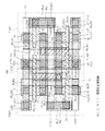
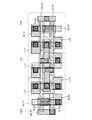
<実施の形態11>
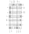
図32〜図34はこの発明の実施の形態11であるSRAMのメモリセル構造を示す図である。図32は全層におけるレイアウト構成を平面視した説明図である。図33は主として図32の第1アルミ配線層下のレイアウト構成を平面視した説明図である。図34は主として図32の第2アルミ配線層上のレイアウト構成を平面視した説明図である。なお、図33,図34で示した符号の一部を図32では省略している場合がある。
【0206】
また、実施の形態11のレイアウト構成のSRAMメモリセルの等価回路は図4で示した実施の形態1と同様である。
【0207】
以下、図32〜図34を参照して、実施の形態11のメモリセル構造について述べる。
【0208】
Nウエル領域NW内において、P+拡散領域FL110,FL111及びポリシリコン配線PL51によりPMOSトランジスタP1を構成し、P+拡散領域FL120,FL121及びポリシリコン配線PL52によりPMOSトランジスタP2を構成する。
【0209】
Pウエル領域PW0内において、N+拡散領域FL210(FL210A,FL210B),FL211及びポリシリコン配線PL51によりNMOSトランジスタN1を構成し、N+拡散領域FL240,FL241及びポリシリコン配線PL54によってNMOSトランジスタN4を構成する。なお、ポリシリコン配線PL51はNウエル領域NWからPウエル領域PW0にかけて形成されることにより、NMOSトランジスタN1及びPMOSトランジスタP1のゲートとして共有される。
【0210】
Pウエル領域PW1内において、N+拡散領域FL220(FL220A,FL220B),FL221及びポリシリコン配線PL52によりNMOSトランジスタN2を構成し、N+拡散領域FL230,FL231及びポリシリコン配線PL53によってNMOSトランジスタN3を構成する。なお、ポリシリコン配線PL52はNウエル領域NWからPウエル領域PW1にかけて形成されることにより、NMOSトランジスタN2及びPMOSトランジスタP2のゲートとして共有される。なお、上記した拡散領域は不純物を注入,拡散することにより得られる。
【0211】
拡散領域FL210A,FL210B上のグランド配線LG1はそれぞれ拡散コンタクトホール1Cを介して拡散領域FL210A,FL210Bに電気的に接続され、拡散領域FL241上のビット線BLB1は拡散コンタクトホール1Cを介して拡散領域FL241に電気的に接続される。
【0212】
拡散領域FL211上から拡散領域FL111上に伸びて形成される第1層アルミ配線であるアルミ配線AL17は、拡散領域FL211と拡散コンタクトホール1Cを介して電気的に接続される。
【0213】
さらに、アルミ配線AL17はポリシリコン配線PL52に電気的に接続される。ポリシリコン配線PL52はシェアードコンタクトSCを介して拡散領域FL111及び拡散領域FL231それぞれに電気的に接続される。
【0214】
アルミ配線AL17は電気的に低インピーダンスな接続が可能であり、アルミ配線AL17、2つのシェアードコンタクトSC及びポリシリコン配線PL52が記憶端子Naに相当する。
【0215】
ポリシリコン配線PL54はゲートコンタクトホールGCを介して、ワード線WL1に電気的に接続される。
【0216】
拡散領域FL110上の電源配線LV1は拡散コンタクトホール1Cを介して拡散領域FL110と電気的に接続され、拡散領域FL121上の電源配線LV1は拡散コンタクトホール1Cを介して拡散領域FL121に電気的に接続される。
【0217】
グランド配線LG1は拡散コンタクトホール1Cを介して拡散領域FL221に電気的に接続され、拡散領域FL230上のビット線BLA1は拡散コンタクトホール1Cを介して拡散領域FL230と電気的に接続される。
【0218】
拡散領域FL220上から拡散領域FL120上に伸びて形成される第1層アルミ配線であるアルミ配線AL18は、拡散領域FL220と拡散コンタクトホール1Cを介して電気的に接続される。
【0219】
さらに、アルミ配線AL18はポリシリコン配線PL51に電気的に接続される。ポリシリコン配線PL51はシェアードコンタクトSCを介して拡散領域FL120及び拡散領域FL240それぞれに電気的に接続される。
【0220】
アルミ配線AL18は電気的に低インピーダンスな接続が可能であり、アルミ配線AL18、2つのシェアードコンタクトSC及びポリシリコン配線PL51が記憶端子Nbに相当する。
【0221】
ポリシリコン配線PL53上のワード線WL1はゲートコンタクトホールGCを介してポリシリコン配線PL53と電気的に接続される。
【0222】
ワード線WL1はビアホール1Tを介してワード線WL2に電気的に接続され、ワード線WL2はビアホール2Tを介してワード線WL3に電気的に接続される。ワード線WL3はウエル領域PW0,PW1及びNウエル領域NWを横断して形成される。
【0223】
ビット線BLA2はビアホール1Tを介してビット線BLA1に電気的に接続され、ビット線BLB2はビアホール1Tを介してビット線BLB1に電気的に接続される。
【0224】
電源配線LV2はビアホール1Tを介して電源配線LV1に電気的に接続される。グランド配線LG1はビアホール1Tを介してグランド配線LG2に電気的に接続される。
【0225】
ビット線BLA2,BLB2、グランド配線LG2及び電源配線LV2は図中縦方向に並行して形成される。
【0226】
ビット線BLA2及びグランド配線LG2はPウエル領域PW1上に形成され、ビット線BLB2及びグランド配線LG2はPウエル領域PW0上に形成され、電源配線LV2はNウエル領域NW上に形成される。
【0227】
このように、実施の形態11のSRAMのメモリセル構造は、NMOSトランジスタN1、N4を一方のPウエル領域PW0内に形成し、NMOSトランジスタN2,N3をNウエル領域NWを挟んだ他方のPウエル領域PW1内に形成することにより、実施の形態1の第1の効果であるソフトエラー耐性が向上を図ることができる。
【0228】
また、Pウエル領域PW0及びPW1を、ビット線BLA,BLBの形成方向に垂直な方向で分離形成することより、実施の形態1の第2の効果である良好なアクセスタイムを維持することができる。
【0229】
また、実施の形態11は、実施の形態1と同様、NMOSトランジスタN1,N2、及びNMOSトランジスタN3,N4はそれぞれメモリセルの中心部に対して点対称となるようにレイアウト配置されるため、実施の形態11のメモリセルを複数個隣接して形成する場合に集積度の向上を図ることができる(実施の形態1の第3の効果に相当)。
【0230】
また、ポリシリコン配線PL51〜PL54をほぼ同一方向(図中横方向)で形成することにより、ゲート寸法の制御が容易になる効果があり、さらに、ポリシリコン配線PL51,PL53、ポリシリコン配線PL52,PL54をそれぞれ一直線上に形成することにより、無駄領域がなくなり、回路面積の削減により集積度の向上を図ることができる(実施の形態1の第4の効果に相当)。
【0231】
加えて、NMOSトランジスタN1〜N4において、ドレインとなる領域を独立して形成することにより、ソフトエラー耐性の高いレベルで維持することができる(実施の形態1の第5の効果に相当)。
【0232】
さらに、CMOS構造のインバータI1,I2をそれぞれNMOSトランジスタ及びPMOSトランジスタ一つずつの組で構成するここにより、CMOS構造として必要最小限の回路構成でメモリセルを実現することができる(実施の形態1の第6の効果に相当)。
【0233】
加えて、記憶端子Naをアルミ配線AL17、シェアードコンタクトSC及びポリシリコン配線PL52で構成し、記憶端子Nbをアルミ配線AL18、シェアードコンタクトSC及びポリシリコン配線PL51で構成することにより、図中縦方向のウェル形成幅を2トランジスタピッチで形成できる分、集積度の向上を図ることができる。
【0234】
<実施の形態12>
図35及び図36はこの発明の実施の形態12であるSRAMのメモリセル構造を示す図である。図35は全層におけるレイアウト構成を平面視した説明図である。図36は主として図35の第2アルミ配線層上のレイアウト構成を平面視した説明図である。なお、主として図35の第1アルミ配線層下のレイアウト構成を平面視した説明図は実施の形態11の説明で用いた図33(ワード線WL2がワード線WLA2,WLB2に分離された点は異なる)と同様であり、図36,図33で示した符号の一部を図35では省略している場合がある。また、実施の形態12のレイアウト構成のSRAMメモリセルの等価回路は実施の形態5で示した図15と同様である。
【0235】
以下、図35,図36及び図33を参照して、実施の形態12のメモリセル構造について述べる。
【0236】
ポリシリコン配線PL53はゲートコンタクトホールGCを介して、ワード線WLA1(図33の右端のワード線WL1に相当)に電気的に接続され、ワード線WLA1はビアホール1Tを介してワード線WLA2に電気的に接続され、ワード線WLA2はビアホール2Tを介してワード線WLA3に電気的に接続される。これらワード線WLA1〜ワード線WLA3によって図15のワード線WLAを構成する。
【0237】
同様にして、ポリシリコン配線PL54はゲートコンタクトホールGCを介して、ワード線WLB1(図33の左端のワード線WL1に相当)に電気的に接続され、ワード線WLB1はビアホール1Tを介してワード線WLB2に電気的に接続され、ワード線WLB2はビアホール2Tを介してワード線WLB3に電気的に接続される。これらワード線WLB1〜WLB3によって図15のワード線WLBを構成する。
【0238】
ワード線WLA3,WLB3はPウエル領域PW0,PW1及びNウエル領域NWを横断して互いに並行に形成される。なお、他のレイアウト構成は実施の形態11と同様であるため説明を省略する。
【0239】
実施の形態12は上記のようなメモリセル構造を有することにより、実施の形態11の効果に加え、実施の形態5と同様、FIFOメモリで利用可能なメモリセル構造を実現することができる。
【0240】
<その他>
なお、上述した実施の形態1〜実施の形態12において、導電型式を全て逆にして構成しても同様な効果を奏する。さらに、MOSトランジスタに限らず、MISトランジスタ等の電界効果トランジスタに対しても同様な効果を奏する。
【0241】
【発明の効果】
以上説明したように、この発明における第1の態様の半導体記憶装置は、第1の記憶端子に一方電極が接続される第1及び第3の第1種電界効果トランジスタを第1及び第2の第2種ウェル領域にそれぞれ分けて形成し、第2の記憶端子に一方電極が接続される第2及び第4の第1種電界効果トランジスタを第2及び第1の第2種ウェル領域にそれぞれ分けて形成している。
【0242】
したがって、α線や中性子線によって発生した電子が、第1及び第2の第2種ウエル領域のうち一方の第2種ウエル領域に形成した第1〜第4の第1種電界効果トランジスタの一方電極領域に収集された場合に、第1種ウエル領域が介在することにより上記電子の発生による影響が防止される他方の第2種ウエル領域に形成した第1〜第4の第1種電界効果トランジスタの一方電極領域から放出される。例えば、第1の第2種ウエル領域内の第1の第1種電界効果トランジスタの一方電極領域に収集された電子は第1の記憶端子を介して第2の第2種ウエル領域内の第3の第1種電界効果トランジスタの一方電極領域から放出され、第2の第2種ウエル領域内の第2の第1種電界効果トランジスタの一方電極領域に収集された電子は第2の記憶端子を介して第1の第2種ウエル領域内の第4の第1種電界効果トランジスタの一方電極領域から放出される。
【0243】
このような動作により、第1及び第2の記憶端子の保持データを反転させようとする電子の発生が相殺されるため、データの反転が起こりにくくなり、その結果、ソフトエラー耐性が向上するという効果を奏する。
【0244】
加えて、第1及び第2のインバータはそれぞれ第1種及び第2種電界効果トランジスタ一つずつの組で構成されているため、相補型の構成では必要最小限の回路構成で実現できる。
【0245】
第2の態様の半導体記憶装置は、第1あるいは第2の記憶端子に接続される一方電極を第1〜第4の第1種電界効果トランジスタ間で互いに独立して形成することにより、ソフトエラー耐性のさらなる向上を図ることができる。
【0246】
第3の態様の半導体記憶装置のように第1〜第4の第1種電界効果トランジスタ及び第1,第2の第2種電界効果トランジスタを配置することにより、集積度の向上を図ることができる。
【0247】
第4の態様の半導体記憶装置は、第1及び第2のMOSトランジスタをメモリセルの中心点に対して互いに点対称となるようにレイアウト配置することにより、隣接するメモリセル間の配置を容易にして集積度の向上を図ることができる。
【0248】
第5の態様の半導体記憶装置は、第3及び第4のMOSトランジスタをメモリセルの中心点に対して互いに点対称となるようにレイアウト配置することにより、隣接するメモリセル間の配置を容易にして集積度の向上を図ることができる。
【0249】
第6の態様の半導体記憶装置は、第1及び第2の第1種電界効果トランジスタの制御電極幅を第3及び第4の第1種電界効果トランジスタの制御電極幅より広く設定することにより、メモリセルの安定性の向上を図ることができる。
【0250】
第7の態様の半導体記憶装置は、第1及び第2の抵抗成分による信号伝播遅延によって、メモリセルの第1及び第2の記憶端子に保持しているデータを反転するための応答特性を長くして、ソフトエラーを起こりにくくすることができる。
【0251】
第8の態様の半導体記憶装置は、高抵抗金属配線によって第1及び第2の抵抗成分を実現している。
【0252】
第9の態様の半導体記憶装置は、高抵抗ポリシリコン配線によって第1及び第2の抵抗成分を実現している。
【0253】
第10の態様の半導体記憶装置は、第3及び第4のMOSトランジスタの制御電極及びワード線を一本のポリシリコンで共用することにより、形成すべき層の数を減少させて装置のコスト削減を図ることができる。
【0254】
第11の態様の半導体記憶装置は、第1及び第2のワード線による2つのメモリセル選択手段を有することにより、メモリセルをFIFOメモリ用に用いることができる。
【0255】
第12の態様の半導体記憶装置は、第1〜第4の部分ビット線及び第1及び第2のワード線による2ポートメモリセルが実現する。
【0256】
第13の態様の半導体記憶装置は、第1及び第2の第1種電界効果トランジスタの制御電極幅を第5〜第8の第1種電界効果トランジスタの制御電極幅より広く設定することにより、メモリセルの安定性の向上を図ることができる。
【0257】
第14の態様の半導体記憶装置は、第1及び第2の第1種電界効果トランジスタの制御電極形成領域を第2及び第1の記憶端子の一部を構成するようにレイアウト配置することにより、メモリセル形成領域を狭くして集積度の向上を図ることができる。
【0258】
第15の態様の半導体記憶装置は、第1及び第2の第2種ウェル領域の間にレイアウト配置された第1種ウェル領域によって、第1及び第2の第2種ウェル領域のうち一方の第2種ウェル領域で生成されたキャリアが他方の第2種ウェル領域に影響を及ぼすことを防止することができる。
【図面の簡単な説明】
【図1】 この発明に実施の形態1であるSRAMのメモリセルの全層におけるレイアウト構成を平面視した説明図である。
【図2】 主として図1の第1アルミ配線層下のレイアウト構成を平面視した説明図である。
【図3】 主として図1の第2アルミ配線層上のレイアウト構成を平面視した説明図である。
【図4】 実施の形態1のメモリセルの等価回路を示す回路図である。
【図5】 実施の形態2のSRAMメモリセルの全層におけるレイアウト構成を平面視した説明図である。
【図6】 主として図5の第1アルミ配線層下のレイアウト構成を平面視した説明図である。
【図7】 隣接するメモリセル間における第1アルミ配線層下のレイアウト構成を平面視した説明図である。
【図8】 実施の形態3のSRAMメモリセルの全層におけるレイアウト構成を平面視した説明図である。
【図9】 主として図8の第1アルミ配線層下のレイアウト構成を平面視した説明図である。
【図10】 実施の形態3のメモリセルの等価回路を示す回路図である。
【図11】 実施の形態4のSRAMメモリセルの全層におけるレイアウト構成を平面視した説明図である。
【図12】 主として図11の第1アルミ配線層下のレイアウト構成を平面視した説明図である。
【図13】 実施の形態5のSRAMメモリセルの全層におけるレイアウト構成を平面視した説明図である。
【図14】 主として図13の第2アルミ配線層上のレイアウト構成を平面視した説明図である。
【図15】 実施の形態5のメモリセルの等価回路を示す回路図である。
【図16】 実施の形態6のSRAMメモリセルの全層におけるレイアウト構成を平面視した説明図である。
【図17】 主として図16の第1アルミ配線層下のレイアウト構成を平面視した説明図である。
【図18】 主として図16の第2アルミ配線層上のレイアウト構成を平面視した説明図である。
【図19】 実施の形態7のSRAMメモリセルの全層におけるレイアウト構成を平面視した説明図である。
【図20】 主として図19の第1アルミ配線層下のレイアウト構成を平面視した説明図である。
【図21】 主として図19の第2アルミ配線層上のレイアウト構成を平面視した説明図である。
【図22】 実施の形態8のSRAMメモリセルの全層におけるレイアウト構成を平面視した説明図である。
【図23】 主として図22の第1アルミ配線層下のレイアウト構成を平面視した説明図である。
【図24】 主として図22の第2アルミ配線層上のレイアウト構成を平面視した説明図である。
【図25】 実施の形態8のメモリセルの等価回路を示す回路図である。
【図26】 実施の形態9のSRAMメモリセルの全層におけるレイアウト構成を平面視した説明図である。
【図27】 主として図26の第1アルミ配線層下のレイアウト構成を平面視した説明図である。
【図28】 主として図26の第2アルミ配線層上のレイアウト構成を平面視した説明図である。
【図29】 実施の形態10のSRAMメモリセルの全層におけるレイアウト構成を平面視した説明図である。
【図30】 主として図29の第1アルミ配線層下のレイアウト構成を平面視した説明図である。
【図31】 主として図29の第2アルミ配線層上のレイアウト構成を平面視した説明図である。
【図32】 実施の形態11のSRAMメモリセルの全層におけるレイアウト構成を平面視した説明図である。
【図33】 主として図32の第1アルミ配線層下のレイアウト構成を平面視した説明図である。
【図34】 主として図32の第2アルミ配線層上のレイアウト構成を平面視した説明図である。
【図35】 実施の形態のSRAMメモリセルの全層におけるレイアウト構成を平面視した説明図である。
【図36】 主として図35の第2アルミ配線層上のレイアウト構成を平面視した説明図である。
【図37】 従来のSRAMメモリセルを示す回路図である。
【符号の説明】
BLA,BLB,バーBLA,バーBLB ビット線、FL110,FL111,FL120,FL121 P+拡散領域、FL210〜FL215,FL220〜FL225,FL230〜FL233,FL240〜FL243 N+拡散領域、I1,I2 インバータ、M00,M01 高抵抗金属配線、N1,N2 NMOSトランジスタ(ドライバトランジスタ)、N3〜N7 NMOSトランジスタ(アクセストランジスタ)、NW Nウエル領域、P1,P2 PMOSトランジスタ(ドライバトランジスタ)、PL5 共用ポリシリコン配線PL5、PL7,PL8 高抵抗ポリシリコン配線、PW0,PW1 Pウエル領域、R1,R2 抵抗、WL,WLA,WLB ワード線。[0001]
BACKGROUND OF THE INVENTION
This inventionHalfThe present invention relates to a conductor device, and more particularly to a memory structure that improves the soft error resistance of a MOS static RAM.
[0002]
[Prior art]
With the miniaturization of memory cells, the problem of soft error that the data held in the storage node is inverted due to the electrons generated by the alpha rays emitted from the package and the neutron rays from the universe has become apparent. It will turn. In particular, as the power supply voltage decreases, the malfunction becomes prominent. Various attempts have been made to reduce soft errors.
[0003]
FIG. 37 is a circuit diagram showing a structure equivalent to, for example, an SRAM memory cell disclosed in Japanese Patent No. 2589949. As shown in the figure, the
[0004]
The sources of the PMOS transistors PT1 and PT2 are commonly connected to the power supply voltage Vcc. The drain of the PMOS transistor PT1 is connected to the gate of the PMOS transistor PT2 and the gates of the NMOS transistors T21 and NT22 via the
[0005]
The sources of the NMOS transistors NT11 and NT12 are both grounded (GND), the drain of the NMOS transistor NT11 is connected to the drain of the PMOS transistor PT1 through the
[0006]
The sources of the NMOS transistors NT21 and NT22 are both grounded, the drain of the NMOS transistor NT21 is connected to the drain of the PMOS transistor PT2 through the
[0007]
NMOS transistor NT5 is inserted between bit line BL50 and
[0008]
In such a configuration, the data obtained from the bit line pair BL50, BL51 or the bit line pair BL60, BL61 is activated, the word line WL50 or the word line WL60 is activated, and the NMOS transistors NT5, NT6 or NMOS transistors NT6, NT8 are turned on. By turning it on, it is possible to access the
[0009]
In the above configuration, the NMOS driver transistor formed of one NMOS transistor is usually divided into two NMOS transistors (NT11 and NT12 and NT21 and NT22).
[0010]
Then, in order to divide the storage node, which is the drain of the PMOS transistor PT1 (PT2), into the node 101 (111) and the node 102 (112), the NMOS transistor NT11 (NT21) and the NMOS transistor NT12 (NT22) are replaced with the PMOS transistor. They are formed on opposite sides of the N well region where PT1 is formed.
[0011]
Therefore, the N-well region has a soft error rate by preventing electrons or holes generated by energetic particles impinging on one side from affecting the depletion region on the opposite side of the N-well region. Can be reduced.
[0012]
[Problems to be solved by the invention]
However, the SRAM memory cell also has a problem that the soft error reduction is not sufficient, and the circuit configuration becomes complicated because the driver transistor which can be originally constituted by two is constituted by two. .
[0013]
The present invention has been made to solve the above-described problems, and has a memory cell structure that reduces soft errors without complicating the circuit configuration.HalfThe object is to obtain a conductor device.
[0028]
ThisClaims related to the invention1The semiconductor device described is2 portsThe static memory cell has a first inverter whose input is connected to a first storage node and whose output is connected to a second storage node, and an input to the second storage node. Is connected to the first storage node, and one end is connected to the first storage node and the other end is connected to the first bit line for the first port. A first transistor of a first conductivity type, connected and having a gate electrode connected to a first word line, one end connected to the first storage node, and the other end connected to a second port A second transistor of the first conductivity type connected to the second bit line, the gate electrode connected to the second word line, one end connected to the second storage node, and the other end to the first Connected to the third bit line for A third transistor of the first conductivity type having a first electrode connected to the first word line, one end connected to the second storage node, and the other end connected to a fourth port for the second port A fourth transistor of the first conductivity type connected to the bit line and having a gate electrode connected to the second word line, and the first word line and the second word line are arranged side by side The static memory cells arrangedIn, First region of second conductivity typeThe secondA second region of one conductivity type,as well asThird region of second conductivity typeButThe first and second word linesofIn the direction of stretchingIn order of the first, second and third regionsPlaced,In the first region, the first transistor, the third transistor, and a fifth transistor of the first conductivity type constituting the second inverter are disposed, and the second region is provided in the second region. Includes a second conductivity type seventh transistor constituting the second inverter and a second conductivity type eighth transistor constituting the first inverter, and the third region includes: The second transistor, the fourth transistor, and a sixth transistor of the first conductivity type constituting the first inverter are arranged.
AlsoAccording to an eighth aspect of the present invention, there is provided a semiconductor device comprising a static random access memory, wherein one memory cell of the static random access memory comprises first to eighth transistors. , First and second well regions of the first conductivity type, and third well regions of the second conductivity type disposed between the first and second well regions, respectively, and the third well regions spaced apart from each other. The first conductivity type first and second impurity regions that are respectively provided in the well region and constitute the electrodes of the first transistor, and are provided in the third well region spaced apart from each other. The third and fourth impurity regions of the first conductivity type constituting the electrodes of the two transistors, respectively, are provided in the first well region so as to be spaced apart from each other, and the electrodes of the third transistor are arranged in the first well region. Second and fifth impurity regions of the second conductivity type, respectively, are provided in the first well region so as to be separated from each other, and second conductivity type of the second conductivity type respectively constituting the electrodes of the fourth transistor. The seventh and eighth impurity regions are provided in the first well region so as to be spaced apart from each other, and constitute the electrodes of the fifth transistor, respectively. Eleventh and twelfth impurity regions of the second conductivity type provided in the second well region and spaced apart from each other and constituting the electrodes of the sixth transistor, respectively, separated from each other in the second well region The second conductivity type thirteenth and fourteenth impurity regions respectively constituting the electrodes of the seventh transistor are provided in the second well region so as to be separated from each other, and Electric On the regions between the first and second impurity regions, and on the region between the fifth and sixth impurity regions, respectively. And a first conductive layer integrally forming the respective gate electrodes of the first and third transistors, a region between the third and fourth impurity regions, and the eleventh and fourth A second conductive layer disposed at least on a region between the twelve impurity regions and integrally forming a gate electrode of each of the second and sixth transistors, and between the seventh and eighth impurity regions. A third conductive layer disposed at least above the region and above the region between the ninth and tenth impurity regions and integrally configuring the gate electrodes of the fourth and fifth transistors, 13th and 14th failure The gate electrode of each of the seventh and eighth transistors is configured to be integrally formed at least on a region between the pure regions and on a region between the fifteenth and sixteenth impurity regions. A fourth conductive layer, the second, sixth, seventh and fifteenth impurity regions and a fifth conductive layer electrically connected to the second conductive layer, the third, ninth, twelfth and A thirteenth impurity region and a sixth conductive layer electrically connected to the first conductive layer are disposed on the first to third well regions, and are electrically connected to the fourth conductive layer. A first word line, a second word line disposed on the first to third well regions apart from the first word line and electrically connected to the third conductive layer. A word line; a first bit line electrically connected to the fourteenth impurity region; A second bit line electrically connected to the pure region, a third bit line electrically connected to the eighth impurity region, and an electrically connected to the tenth impurity region A fourth bit line, the first and second impurity regions facing each other, the third and fourth impurity regions facing each other, and the fifth and sixth impurity regions mutually. A direction facing each other, a direction facing each other of the seventh and eighth impurity regions, a direction facing each other of the ninth and tenth impurity regions, a direction facing each other of the eleventh and twelfth impurity regions, The direction in which the thirteenth and fourteenth impurity regions face each other and the direction in which the fifteenth and sixteenth impurity regions face each other are the same direction.
[0029]
DETAILED DESCRIPTION OF THE INVENTION
<
1 to 4 are diagrams showing the SRAM memory cell structure according to the first embodiment of the present invention. FIG. 1 is an explanatory diagram viewed from above the layout configuration in all layers. FIG. 2 is an explanatory diagram viewed from above mainly the layout configuration below the first aluminum wiring layer of FIG. FIG. 3 is an explanatory diagram viewed from above mainly the layout configuration on the second aluminum wiring layer of FIG. 2 may be omitted in FIG. 1 in some cases.
[0030]
FIG. 4 is a circuit diagram showing an equivalent circuit of the SRAM memory cell having the layout configuration shown in FIGS. As shown in the figure, the SRAM memory cell of the first embodiment includes NMOS transistors N1 to N4 and PMOS transistors P1 and P2.
[0031]
PMOS transistors P1 and P2 which are driver transistors are formed in the N well region NW, NMOS transistor N1 which is the driver transistor and NMOS transistor N4 which is the access transistor are formed in the P well region PW0, and NMOS which is the driver transistor. Transistor N2 and NMOS transistor N3, which is an access transistor, are formed in P well region PW1. P well region PW0 and P well region PW1 are formed on opposite sides of N well region NW.
[0032]
The NMOS transistor N1 and the PMOS transistor P1 constitute a first CMOS inverter I1. That is, the gates of the PMOS transistor P1 and the NMOS transistor N1 are commonly connected to the storage terminal Nb, and the drains are commonly connected to the storage terminal Na. The source of the PMOS transistor P1 is connected to the power supply voltage Vdd, and the source of the NMOS transistor N1 is grounded (GND).
[0033]
The NMOS transistor N2 and the PMOS transistor P2 constitute a second CMOS inverter I2. That is, the gates of the PMOS transistor P2 and the NMOS transistor N2 are commonly connected to the storage terminal Na, and the drains are commonly connected to the storage terminal Nb. The source of the PMOS transistor P2 is connected to the power supply voltage Vdd, and the source of the NMOS transistor N2 is grounded.
[0034]
Thus, the output part of the inverter I1 and the input part of the inverter I2 are electrically connected to the storage terminal Na, and the input part of the inverter I1 and the output part of the inverter I2 are electrically connected to the storage terminal Nb. The CMOS inverters I1 and I2 are cross-connected to each other, and can invert information of logic levels inverted from each other in the storage terminal Na and the storage terminal Nb.
[0035]
The NMOS transistor N3 is interposed between the bit line BLA and the storage terminal Na, and the gate is connected to the word line WL. The NMOS transistor N4 is inserted between the bit line BLB and the storage terminal Nb, and its gate is connected to the word line WL.
[0036]
In such a configuration, the data obtained from the bit line BLA or the bit line BLB is accessed to the storage terminal Na and the storage terminal Nb by activating the word line WL and turning on the NMOS transistors N3 and N4 ( Read or write).
[0037]
The memory cell structure of the first embodiment will be described below with reference to FIGS.
[0038]
In the N well region NW, P+The diffusion region FL110, FL111 and the polysilicon wiring PL1 constitute a PMOS transistor P1, and P+The diffusion regions FL120 and FL121 and the polysilicon wiring PL2 constitute a PMOS transistor P2.
[0039]
In the P well region PW0, N+The diffusion regions FL210 and FL211 and the polysilicon wiring PL1 constitute an NMOS transistor N1, and N+The diffusion regions FL240 and FL241 and the polysilicon wiring PL4 constitute an NMOS transistor N4. The polysilicon wiring PL1 is formed from the N well region NW to the P well region PW0, and is thus shared as the gates of the NMOS transistor N1 and the PMOS transistor P1.
[0040]
In the P well region PW1, N+The diffusion region FL220, FL221 and the polysilicon wiring PL2 constitute an NMOS transistor N2, and N+The diffusion regions FL230 and FL231 and the polysilicon wiring PL3 constitute an NMOS transistor N3. Note that the polysilicon wiring PL2 is formed from the N well region NW to the P well region PW1, thereby being shared as the gates of the NMOS transistor N2 and the PMOS transistor P2.
[0041]
The diffusion regions FL110, FL111, FL120, FL121, FL210, FL211, FL220, FL221, FL230, FL231, FL240, FL241 are obtained by implanting and diffusing impurities.
[0042]
Ground wiring LG1 (first layer aluminum wiring) on diffusion region FL210 is electrically connected to diffusion region FL210 through
[0043]
The
[0044]
Polysilicon wiring PL4 is electrically connected to word line WL1 (first layer aluminum wiring) through gate contact hole GC, and bit line BLB1 (first layer aluminum wiring) on diffusion region FL241 is
[0045]
Aluminum wiring AL12, which is a first layer aluminum wiring formed extending from diffusion region FL240 to diffusion region FL120 and diffusion region FL220, is connected to each diffusion region FL240, FL120, and FL220 via
[0046]
Power supply wiring LV1 (first layer aluminum wiring) on diffusion region FL110 is electrically connected to diffusion region FL110 through
[0047]
Bit line BLA1 (first layer aluminum wiring) on diffusion region FL230 is electrically connected to diffusion region FL230 via
[0048]
The ground wiring LG1 is electrically connected to the ground wiring LG2 (second layer aluminum wiring (2AL)) through the via
[0049]
The word line WL1 is electrically connected to the word line WL2 (second layer aluminum wiring) via the via
[0050]
The via
[0051]
The word line WL3 and the ground wiring LG3 are formed in parallel with each other across the P well regions PW0, PW1 and the N well region NW, and two ground wirings LG3 are formed with the word line WL3 interposed therebetween.
[0052]
Bit line BLA2 (second layer aluminum wiring) is electrically connected to bit line BLA1 (not shown in FIG. 3) via via
[0053]
The bit lines BLA2 and BLB2 and the power supply wiring LV2 are formed on the P well regions PW1 and PW0 and the N well region NW in parallel with each other in the vertical direction in the drawing.
[0054]
As described above, in the SRAM memory cell structure of the first embodiment, the NMOS transistors N1 and N4 are formed in one P well region PW0, and the NMOS transistors N2 and N3 are formed in the other P well with the N well region NW interposed therebetween. N that is electrically connected to the storage terminal Na by being formed in the region PW1+Diffusion regions FL211 and N+Diffusion region FL231 is formed separately in different P well regions PW0 and PW1, and N electrically connected to storage terminal Nb+Diffusion regions FL240 and N+Diffusion region FL220 can be formed separately in different P well regions PW0 and PW1.
[0055]
As a result, electrons generated by α rays and neutron rays are formed in one of the P well regions PW0 and PW1 in the P well region.+When collected in the diffusion region, the N well region NW is formed, and the N well formed in the other P well region is prevented from being affected by the generation of electrons.+Released from the diffusion region. For example, electrons collected in the diffusion region FL211 of the P well region PW0 are emitted from the diffusion region FL231 of the P well region PW1 through the storage terminal Na, and electrons collected in the diffusion region FL220 of the P well region PW1 are stored in the storage terminal Released from diffusion region FL240 of P well region PW0 through Nb.
[0056]
Such an operation cancels out the generation of electrons that attempt to invert the data held in the storage terminals Na and Nb, so that the inversion of data hardly occurs. That is, there is an effect that soft error resistance is improved (first effect).
[0057]
Further, by separating the P well region PW0 and the P well region PW1 in a direction perpendicular to the direction in which the bit lines BLA and BLB are formed, the two P well regions PW0 and PW1 are formed on the bit lines BLA and BLB. No effect on the length. Therefore, the formation of the P well regions PW0 and PW1 does not increase the wiring length of the bit line, and a good access time can be maintained (second effect).
[0058]
Since the NMOS transistors N1 and N2 and the NMOS transistors N3 and N4 are laid out so as to be point-symmetric with respect to the central portion of the memory cell (the central portion of the N well region NW), the memory according to the first embodiment. When a plurality of cells are formed adjacent to each other, the degree of integration can be improved (third effect).
[0059]
In addition, forming the polysilicon wirings PL1 to PL4 in the same direction (lateral direction in the figure) has an effect of facilitating the control of the gate dimensions. Further, the polysilicon wirings PL1, PL3 (NMOS transistors N1, N3,. By forming the PMOS transistor P1) and the polysilicon wirings PL2 and PL4 (NMOS transistors N2 and N4, PMOS transistor P2) on a straight line, there is no wasted area, and the degree of integration can be improved by reducing the circuit area. Yes (fourth effect).
[0060]
In addition, in the NMOS transistors N1 to N4, a region serving as a drain (a region electrically connected to the storage terminal Na or the storage terminal Nb) is independently formed to maintain a high level of soft error resistance. (Fifth effect).
[0061]
Furthermore, by configuring each of the inverters I1 and I2 having a CMOS structure as a set of one NMOS transistor and one PMOS transistor, a memory cell can be realized with a minimum circuit configuration as a CMOS structure (sixth effect). ).
[0062]
<
5 and 6 are diagrams showing the memory cell structure of the SRAM according to the second embodiment of the present invention. FIG. 5 is an explanatory diagram viewed from above the layout configuration in all layers. FIG. 6 is an explanatory diagram viewed from above mainly the layout configuration below the first aluminum wiring layer of FIG. Note that an explanatory diagram viewed mainly from the layout configuration on the second aluminum wiring layer in FIG. 5 is the same as FIG. 3 used in the description of the first embodiment, and a circuit diagram showing an equivalent circuit of the second embodiment is as follows. The same as FIG. 6 and FIG. 3 may be partially omitted in FIG.
[0063]
As shown in these figures, the square N for the NMOS transistor N1+The polysilicon wiring PL1 is formed on the diffusion region with the N+By being bent at the center of the diffusion region, a relatively wide diffusion region FL212 is formed outside the polysilicon wiring PL1, and a relatively narrow diffusion region FL213 is formed inside. The diffusion regions FL212 and FL213 and the polysilicon wiring PL1 constitute an NMOS transistor N1.
[0064]
Similarly, a square N for the NMOS transistor N2+The polysilicon wiring PL2 is formed on the diffusion region with the N+By being bent at the center of the diffusion region, a relatively wide diffusion region FL213 is formed outside the polysilicon wiring PL2, and a relatively narrow diffusion region FL222 is formed inside. The diffusion regions FL222 and FL223 and the polysilicon wiring PL2 constitute an NMOS transistor N2.
[0065]
The ground wiring LG1 on the diffusion region FL212 is electrically connected to the diffusion region FL212 through two
[0066]
Similarly, the ground wiring LG1 on the diffusion region FL223 is electrically connected to the diffusion region FL223 via the two
[0067]
The second embodiment has the following effects in addition to the first, second, fifth and sixth effects of the first embodiment by configuring the layout as described above.
[0068]
The gate width (channel width) W of the NMOS transistors N1 and N2 which are driver transistors can be increased. As a result, the operation speed can be increased by quickly extracting the carriers of the bit lines BLA and BLB.
[0069]
In addition, since the ratio of the gate width W of the NMOS transistors N1 and N2 as driver transistors to the NMOS transistors N3 and N4 as access transistors can be increased, the stability of the memory cell is also improved.
[0070]
FIG. 7 is an explanatory diagram illustrating a layout configuration between adjacent cells. 7 mainly shows the layout configuration below the first aluminum wiring layer in FIG. 5, as in FIG.
[0071]
FIG. 7 shows the N well region NW and P well region PW0 of the memory cell MC1, and the N well region NW and P well region PW0 of the memory cell MC2.
[0072]
At this time, the NMOS transistors N1 and N2 are laid out so as to be point-symmetric with respect to the center portion of the memory cell (center portion of the N well region NW) (corresponding to the third effect of the first embodiment). ). For this reason, as shown in FIG. 7, between adjacent memory cells MC1 and MC2, NMOS transistors N1 (N2) which are driver transistors are connected to a diffusion region FL212, a word line WL1, a ground wiring LG1, a
[0073]
Thus, there is almost no increase in area due to the bending of the polysilicon wirings PL1 and PL2 that serve as the gates of the NMOS transistors N1 and N2, and a high-density memory cell structure equivalent to that of the first embodiment can be obtained. it can.
[0074]
Further, the degree of integration can be improved by forming the NMOS transistors N1, N3, the PMOS transistor P1, the NMOS transistors N2, N4, and the PMOS transistor P2 almost on a straight line (fourth embodiment of the first embodiment). Equivalent to the effect).
[0075]
<Embodiment 3>
8 to 10 are diagrams showing the SRAM memory cell structure according to the third embodiment of the present invention. FIG. 8 is an explanatory diagram viewed from above the layout configuration in all layers. FIG. 9 is an explanatory diagram viewed from above mainly the layout configuration below the first aluminum wiring layer of FIG. 8 is mainly the same as FIG. 3 used in the description of the first embodiment, and a part of the reference numerals shown in FIG. 9 and FIG. May be omitted in FIG.
[0076]
FIG. 10 is a circuit diagram showing an equivalent circuit of the SRAM memory cell having the layout configuration shown in FIG. 8, FIG. 9, and FIG. As shown in the figure, a resistor R1 is inserted between the gates of the NMOS transistor N1 and the PMOS transistor P1 and the storage terminal Nb, and a resistor R2 is inserted between the gates of the NMOS transistor N2 and the PMOS transistor P2 and the storage terminal Na. Is inserted. Other configurations are the same as those of the first embodiment shown in FIG.
[0077]
The memory cell structure of the third embodiment will be described below with reference to FIGS.
[0078]
As shown in these drawings, the polysilicon wiring PL13 (corresponding to the polysilicon wiring PL1 in the first embodiment) serving as the gates of the NMOS transistor N1 and the PMOS transistor P1 is electrically connected to the high resistance metal wiring M00 serving as the resistor R1. The high resistance metal wiring M00 is electrically connected to the aluminum wiring AL12 which is the storage terminal Nb through the via hole 0T. The via hole 0T means a via hole for connection between the high resistance metal wiring M00 formed in the same layer as the polysilicon wiring and the first layer wiring.
[0079]
Similarly, the polysilicon wiring PL14 (corresponding to the polysilicon wiring PL2 of the first embodiment) serving as the gates of the NMOS transistor N2 and the PMOS transistor P2 is electrically connected to the high resistance metal wiring M01 serving as the resistor R2, and this High resistance metal interconnection M01 is electrically connected to aluminum interconnection AL11 which is storage terminal Na through via hole 0T.
[0080]
The material for forming the high resistance metal wirings M00 and M01 is, for example, CoSi such as tungsten.2A material having a higher resistivity than (cobalt silicide) can be used. Other configurations are the same as those in the first embodiment shown in FIGS.
[0081]
In addition to the first to sixth effects of the first embodiment, the third embodiment has the following effects by having the memory cell structure as described above.
[0082]
In the memory cell of the third embodiment, the response characteristic for inverting the data held in the cell becomes long due to the signal delay propagated through the resistors R1 and R2. As a result, even if the potential of one of the storage terminals Na and Nb is inverted by electrons generated by α rays or neutron beams, the original holding state is restored before the data of the other storage terminal is inverted. Therefore, soft errors are less likely to occur.
[0083]
<Embodiment 4>
11 and 12 are diagrams showing the SRAM memory cell structure according to the fourth embodiment of the present invention. FIG. 11 is an explanatory diagram viewed from above the layout configuration in all layers. FIG. 12 is an explanatory diagram viewed from above mainly the layout configuration below the first aluminum wiring layer of FIG. 11 is mainly the same as FIG. 3 used in the description of the first embodiment, and a part of the reference numerals shown in FIG. 12 and FIG. May be omitted in FIG. The equivalent circuit of the SRAM memory cell having the layout configuration of the fourth embodiment is the same as that of FIG. 10 shown in the third embodiment.
[0084]
The memory cell structure of the fourth embodiment will be described below with reference to FIGS.
[0085]
As shown in these drawings, among the polysilicon wirings PL13 and PL17 (corresponding to the polysilicon wiring PL1 of the first embodiment) serving as the gates of the NMOS transistor N1 and the PMOS transistor P1, the polysilicon wiring PL17 serving as the resistor R1 is It is formed of a material having a higher resistance than the polysilicon wiring PL13. For example, the polysilicon wiring PL13 is replaced with CoSi.2When the polysilicon wiring PL17 is formed by CoSi,2It is formed using a forming material having a higher resistivity.
[0086]
The polysilicon wiring PL17 is electrically connected to the aluminum wiring AL12 which is the storage terminal Nb through the gate contact hole GC.
[0087]
Similarly, of the polysilicon wirings PL14 and PL18 (corresponding to the polysilicon wiring PL2 of the first embodiment) serving as the gates of the NMOS transistor N2 and the PMOS transistor P2, the polysilicon wiring PL18 serving as the resistor R2 is the polysilicon wiring PL14. The polysilicon wiring PL18 is electrically connected to the aluminum wiring AL11 that is the storage terminal Na through the gate contact hole GC. Other configurations are the same as those of the first embodiment shown in FIGS.
[0088]
In addition to the first to sixth effects of the first embodiment, the fourth embodiment has the following effects by having the memory cell structure as described above.
[0089]
The memory cell of the fourth embodiment has a long response characteristic for inverting the data held in the cell by the signal delay propagating through the resistors R1 and R2. As a result, even if the potential of one of the storage terminals Na and Nb is inverted by electrons generated by α rays or neutron beams, the original holding state is restored before the data of the other storage terminal is inverted. Therefore, soft errors are less likely to occur.
[0090]
<Embodiment 5>
13 to 15 are diagrams showing the SRAM memory cell structure according to the fifth embodiment of the present invention. FIG. 13 is an explanatory diagram viewed from above the layout configuration in all layers. FIG. 14 is an explanatory diagram viewed from above mainly the layout configuration on the second aluminum wiring layer of FIG. 13 is mainly a plan view of the layout configuration below the first aluminum wiring layer in FIG. 13 (the difference is that word line WL2 is separated into word lines WLA2 and WLB2 used in the description of the first embodiment). ), And some of the reference numerals shown in FIGS. 14 and 2 may be omitted in FIG.
[0091]
FIG. 15 is a circuit diagram showing an equivalent circuit of the SRAM memory cell having the layout configuration shown in FIG. 13, FIG. 14, and FIG. As shown in the figure, the word line WLA is connected to the gate of the NMOS transistor N3, and the word line WLB independent of the word line WLA is connected to the gate of the NMOS transistor N4. Other configurations are the same as those of the first embodiment shown in FIG.
[0092]
The memory cell structure of the fifth embodiment will be described below with reference to FIGS.
[0093]
Polysilicon wiring PL3 is electrically connected to word line WLA1 (first layer aluminum wiring) via gate contact hole GC, and word line WLA1 is connected to word line WLA2 (second layer aluminum wiring) via via
[0094]
Similarly, the polysilicon wiring PL4 is electrically connected to the word line WLB1 (first layer aluminum wiring) via the gate contact hole GC, and the word line WLB1 is connected to the word line WLB2 (second layer via the via
[0095]
The word lines WLA3 and WLB3 and the ground wiring LG3 are formed in parallel with each other across the P well regions PW0 and PW1 and the N well region NW, and two ground wirings LG3 are formed with the word lines WLA3 and WLB3 interposed therebetween. Since other layout configurations are the same as those in the first embodiment, description thereof is omitted.
[0096]
In addition to the first to sixth effects of the first embodiment, the fifth embodiment has the following effects by having the memory cell structure as described above.
[0097]
As shown in the equivalent circuit of FIG. 15, by separating the word lines connected to the gates of the NMOS transistors N3 and N4, which are access transistors, from WLA and WLB, a memory cell structure usable in the FIFO memory can be realized. .
[0098]
<Embodiment 6>
16 to 18 are views showing the memory cell structure of the SRAM according to the sixth embodiment of the present invention. FIG. 16 is an explanatory diagram viewed from above the layout configuration in all layers. FIG. 17 is an explanatory diagram viewed from above mainly the layout configuration below the first aluminum wiring layer of FIG. FIG. 18 is an explanatory diagram viewed from above mainly the layout configuration on the second aluminum wiring layer of FIG. Note that some of the reference numerals shown in FIGS. 17 and 18 may be omitted in FIG. The equivalent circuit of the SRAM memory cell having the layout configuration of the sixth embodiment is the same as that of FIG. 15 shown in the fifth embodiment.
[0099]
The memory cell structure of the sixth embodiment will be described below with reference to FIGS.
[0100]
N for NMOS transistors N3 and N4+The diffusion region is formed by changing the source / drain region formation direction by 90 degrees from the source / drain region formation direction of the other NMOS transistors N1, N2 and PMOS transistors P1, P2. That is, diffusion regions FL242 and FL243 for the NMOS transistor N3 and diffusion regions FL232 and FL233 for the NMOS transistor N4 are formed in the horizontal direction in the drawing.
[0101]
The bit line BLB1 on the diffusion region FL243 is electrically connected to the diffusion region FL243 via the
[0102]
Similarly, the bit line BLA1 on the diffusion region FL232 constituting the NMOS transistor N3 is electrically connected to the diffusion region FL232 via the
[0103]
Bit lines BLA2 and BLB2 are formed in parallel with each other across P well regions PW0 and PW1 and N well region NW.
[0104]
The ground wiring LG1 is electrically connected to the diffusion region FL210 and the diffusion region FL221 through the
[0105]
The power supply wiring LV1 is electrically connected to the diffusion regions FL110 and FL121 via the
[0106]
The word line WLA1 is electrically connected to the polysilicon wiring PL23 via the gate contact hole GC, and the word line WLA2 is electrically connected to the word line WLA1 (not shown in FIG. 18) via the via
[0107]
Similarly, the word line WLB1 is electrically connected to the polysilicon wiring PL24 via the gate contact hole GC, and the word line WLB2 is electrically connected to the word line WLB1 (not shown in FIG. 18) via the via
[0108]
The (first) ground line LG3, the word line WLB3, the power supply line LV3, the word line WLA3, and the (second) ground line LG3 are respectively formed in parallel in the vertical direction in the figure, and the (first) ground line LG3 and The word line WLB3 is formed on the P well region PW0, the power supply wiring LV3 is formed on the N well region NW, and the word line WLA3 and the (second) ground wiring LG3 are formed on the P well region PW1.
[0109]
Since the sixth embodiment has the memory cell structure as described above, in addition to the first to third, fifth, and sixth effects of the first embodiment, the same effects as the effects unique to the fifth embodiment can be obtained. Play.
[0110]
<Embodiment 7>
19 to 21 are views showing the memory cell structure of the SRAM according to the seventh embodiment of the present invention. FIG. 19 is an explanatory diagram viewed from above the layout configuration in all layers. FIG. 20 is an explanatory diagram viewed from above mainly the layout configuration below the first aluminum wiring layer of FIG. FIG. 21 is an explanatory diagram viewed from above mainly the layout configuration on the second aluminum wiring layer of FIG. Note that some of the reference numerals shown in FIGS. 20 and 21 may be omitted in FIG. The equivalent circuit of the SRAM memory cell having the layout configuration of the seventh embodiment is the same as that of FIG. 4 shown in the first embodiment.
[0111]
The memory cell structure of the seventh embodiment will be described below with reference to FIGS.
[0112]
A shared polysilicon wiring PL5 for NMOS transistors N3 and N4 is formed extending from the P well region PW0 to the N well region NW and the P well region PW1, and this shared polysilicon wiring PL5 is used as the word line WL in FIG.
[0113]
Other configurations include the pattern shape of the polysilicon wirings PL1 and PL2, the formation position of the gate contact hole GC between the polysilicon wiring PL1 and the aluminum wiring AL12, and the formation position of the gate contact hole GC between the polysilicon wiring PL2 and the aluminum wiring AL11. Except for, the second embodiment is the same as the second embodiment shown in FIGS.
[0114]
Since the seventh embodiment has the memory cell structure as described above, the same effect as that of the second embodiment can be obtained. Furthermore, since the via holes 1T and 2T and the word lines WL2 and WL3 are not necessary for the word line WL, there is an effect that the number of necessary layers is reduced and the cost can be reduced.
[0115]
<Eighth embodiment>
22 to 25 are views showing the memory cell structure of the SRAM according to the eighth embodiment of the present invention. FIG. 22 is an explanatory diagram viewed from above the layout configuration in all layers. FIG. 23 is an explanatory diagram viewed from above mainly the layout configuration below the first aluminum wiring layer of FIG. FIG. 24 is an explanatory diagram viewed from above mainly the layout configuration on the second aluminum wiring layer of FIG. Note that some of the reference numerals shown in FIGS. 23 and 24 may be omitted in FIG.
[0116]
FIG. 25 is a circuit diagram showing an equivalent circuit of the SRAM memory cell having the layout configuration shown in FIGS. As shown in the figure, the SRAM memory cell of the eighth embodiment includes NMOS transistors N1, N2, N5 to N8 and PMOS transistors P1, P2.
[0117]
The NMOS transistor N5 is inserted between the bit line BLA and the storage terminal Nb, the NMOS transistor N6 is inserted between the bit line bar BLA and the storage terminal Na, and the gates of the NMOS transistors N5 and N6 are commonly connected to the word line WLA. Is done.
[0118]
The NMOS transistor N7 is inserted between the bit line BLB and the storage terminal Na, the NMOS transistor N8 is inserted between the bit line bar BLB and the storage terminal Nb, and the gates of the NMOS transistors N7 and N8 are commonly connected to the word line WLB. Is done.
[0119]
PMOS transistors P1 and P2 as driver transistors are formed in the N well region NW, and NMOS transistors N1 as driver transistors and NMOS transistors N7 and N8 as access transistors are formed in the P well region PW0. An NMOS transistor N2 and NMOS transistors N5 and N6 which are access transistors are formed in the P well region PW1. P well region PW0 and P well region PW1 are formed on opposite sides of N well region NW. Other configurations are the same as those of the equivalent circuit of the fifth embodiment shown in FIG.
[0120]
The memory cell structure according to the eighth embodiment will be described below with reference to FIGS.
[0121]
In the N well region NW, P+The diffusion regions FL110 and FL111 and the polysilicon wiring PL17 constitute a PMOS transistor P1, and P+The diffusion regions FL120 and FL121 and the polysilicon wiring PL18 constitute a PMOS transistor P2.
[0122]
In the P well region PW0, N+The diffusion region FL212, FL213 and the polysilicon wiring PL17 constitute an NMOS transistor N1, and N+The diffusion region FL244, FL245 and the polysilicon wiring PL20 constitute an NMOS transistor N7, and N+Diffusion regions FL246, FL247 and polysilicon wiring PL20 constitute NMOS transistor N8. The polysilicon wiring PL17 is formed from the N well region NW to the P well region PW0, so that it is shared as the gates of the NMOS transistor N1 and the PMOS transistor P1, and the polysilicon wiring PL20 is shared between the NMOS transistors N7 and N8. The
[0123]
In the P well region PW1, N+The diffusion regions FL222 and FL223 and the polysilicon wiring PL18 constitute an NMOS transistor N2, and N+The diffusion region FL234, FL235 and the polysilicon wiring PL19 constitute an NMOS transistor N5, and N+Diffusion regions FL236, FL237 and polysilicon wiring PL19 constitute NMOS transistor N3. The polysilicon wiring PL18 is formed from the N well region NW to the P well region PW1, thereby being shared as the gates of the NMOS transistor N2 and the PMOS transistor P2, and the polysilicon wiring PL18 is shared between the NMOS transistors N5 and N6. The The diffusion region described above can be obtained by implanting and diffusing impurities.
[0124]
The ground wiring LG1 on the diffusion region FL212 is electrically connected to the diffusion region FL212 via two
[0125]
Aluminum wiring AL15, which is a first layer aluminum wiring formed extending from diffusion region FL244 to diffusion region FL213, diffusion region FL111, and diffusion region FL237, has diffusion regions FL244, FL213, FL111, and FL237, respectively. Are electrically connected through the
[0126]
Polysilicon wiring PL20 is electrically connected to word line WLB1 through gate contact hole GC.
[0127]
Power supply line LV1 on diffusion region FL110 is electrically connected to diffusion region FL110 via
[0128]
The ground line LG1 is electrically connected to the diffusion region FL223 via two
[0129]
Aluminum wiring AL16, which is a first layer aluminum wiring formed extending from diffusion region FL235 to diffusion region FL222, diffusion region FL120, and diffusion region FL246, has diffusion regions FL235, FL222, FL120, and FL246, respectively. Are electrically connected through the
[0130]
Word line WLA1 on polysilicon wiring PL19 is electrically connected to polysilicon wiring PL19 via gate contact hole GC.
[0131]
The ground wiring LG1 is electrically connected to the ground wiring LG2 via the via
[0132]
The word line WLA1 is electrically connected to the word line WLA2 via the via
[0133]
Similarly, the word line WLB1 is electrically connected to the word line WLB2 via the via
[0134]
The word lines WLA3 and WLB3 and the ground wiring LG3 are formed in parallel with each other across the P well regions PW0 and PW1 and the N well region NW, and two ground wirings LG3 are formed with the word lines WLA3 and WLB3 interposed therebetween.
[0135]
Bit line BLA2 is electrically connected to bit line BLA1 via via
[0136]
Similarly, the bit line bar BLA2 is electrically connected to the bit line bar BLA1 via the via
[0137]
The power supply wiring LV2 is electrically connected to the power supply wiring LV1 through the via
[0138]
The bit line pair BLA2, the bar BLA2, the bit line pair BLB2, the bar BLB2 and the power supply wiring LV2 are formed in parallel to each other in the vertical direction in the figure on the P well regions PW1, PW0 and the N well region NW, respectively.
[0139]
Thus, in the SRAM memory cell structure of the eighth embodiment, NMOS transistors N1, N7, N8 are formed in one P well region PW0, and NMOS transistors N2, N5, N6 are sandwiched between N well regions NW. N formed in the other P well region PW1 is electrically connected to the storage terminal Na.+Diffusion regions FL213 and FL244 and N+Diffusion region FL237 is formed separately in different P well regions PW0 and PW1, and N electrically connected to storage terminal Nb+Diffusion regions FL222 and FL235 and N+Diffusion region FL246 can be formed separately in different P well regions PW1 and PW0.
[0140]
As a result, the soft error resistance, which is the first effect of the first embodiment, can be improved.
[0141]
Further, by separating the P well regions PW0 and PW1 in the direction perpendicular to the direction in which the bit line pair BLA and bar BLA and the bit line pair BLB and bar BLB are formed, two P well regions PW0 and PW1 are formed. It does not affect the wiring length of the bit line pair BLA and bar BLA and the bit line pair BLB and bar BLB. Therefore, the formation of the P well regions PW0 and PW1 does not increase the wiring length of the bit line, and the good access time as the second effect of the first embodiment can be maintained.
[0142]
Also, the NMOS transistors N1, N2, NMOS transistors N5, N7, and NMOS transistors N6, N8 are laid out so as to be symmetric with respect to the center of the memory cell (the center of the N well region NW). When a plurality of memory cells according to the eighth embodiment are formed adjacent to each other, the degree of integration can be improved (corresponding to the third effect of the first embodiment).
[0143]
In addition, forming the polysilicon wirings PL17 to PL20 in the same direction (lateral direction in the figure) has an effect of facilitating the control of the gate dimensions, and further, polysilicon wirings PL17 and PL19, polysilicon wirings PL18 and PL20. By forming each on a straight line, there is no useless area, and the degree of integration can be improved by reducing the circuit area (corresponding to the fourth effect of the first embodiment).
[0144]
Further, by forming the drain region independently in the NMOS transistors N1, N2, N5 to N8, it can be maintained at a high level of soft error resistance (corresponding to the fifth effect of the first embodiment). ).
[0145]
Further, each of the inverters I1 and I2 having a CMOS structure is formed of a set of one NMOS transistor and one PMOS transistor, whereby a memory cell can be realized with a minimum circuit configuration as a CMOS structure (Embodiment 1). Equivalent to the sixth effect).
[0146]
In addition, the memory cell of the eighth embodiment includes two word lines WLA and WLB and two bit line pairs (bit line pair BLA and bar BLA and bit line pair BLB and bar BLB) as shown in FIG. The two-port memory cell used is realized.
[0147]
<Embodiment 9>
26 to 28 are views showing the memory cell structure of the SRAM according to the ninth embodiment of the present invention. FIG. 26 is an explanatory diagram viewed from above the layout configuration in all layers. FIG. 27 is an explanatory diagram viewed from above mainly the layout configuration below the first aluminum wiring layer of FIG. FIG. 28 is an explanatory diagram viewed from above mainly the layout configuration on the second aluminum wiring layer of FIG. Note that some of the reference numerals shown in FIGS. 27 and 28 may be omitted in FIG.
[0148]
The equivalent circuit of the SRAM memory cell having the layout configuration of the ninth embodiment is the same as that of the eighth embodiment shown in FIG.
[0149]
Hereinafter, the memory cell structure of the ninth embodiment will be described with reference to FIGS. 26 to 28, focusing on a configuration different from that of the eighth embodiment.
[0150]
In the P well region PW0, N+The diffusion regions FL214 and FL215 and the polysilicon wiring PL31 constitute an NMOS transistor N1. At this time, the polysilicon wiring PL31 is connected to N for the NMOS transistor N1.+The gate width is set to be considerably larger than that of the other NMOS transistors N5 to N8 by being bent twice 90 degrees on the diffusion region (FL214, FL215).
[0151]
N+The diffusion regions FL270 and FL271 and the polysilicon wiring PL37 constitute an NMOS transistor N7, and N+Diffusion regions FL280 and FL281 and polysilicon wiring PL38 constitute NMOS transistor N8.
[0152]
The polysilicon wiring PL31 is formed from the N well region NW to the P well region PW0, and is thus shared as the gates of the NMOS transistor N1 and the PMOS transistor P1.
[0153]
In the P well region PW1, N+The diffusion regions FL224 and FL225 and the polysilicon wiring PL32 constitute an NMOS transistor N2. At this time, the polysilicon wiring PL32 is connected to N for the NMOS transistor N2.+By forming it bent 90 degrees twice on the diffusion region (FL224, FL225), a considerably larger gate width is set as compared with the other NMOS transistors N5 to N8.
[0154]
N+The diffusion region FL250, FL251 and the polysilicon wiring PL35 constitute an NMOS transistor N5, and N+The diffusion regions FL260 and PL261 and the polysilicon wiring PL36 constitute an NMOS transistor N6.
[0155]
Note that the polysilicon wiring PL32 is formed from the N well region NW to the P well region PW1, thereby being shared as the gates of the NMOS transistor N2 and the PMOS transistor P2. The diffusion region described above can be obtained by implanting and diffusing impurities.
[0156]
Two ground lines LG1 on diffusion region FL214 are electrically connected to diffusion region FL214 via
[0157]
Aluminum wiring AL17, which is a first layer aluminum wiring formed extending from diffusion region FL281 to diffusion region FL215, diffusion region FL111, and diffusion region FL251, has diffusion regions FL281, FL215, FL111, and FL251, respectively. Are electrically connected through the
[0158]
Polysilicon wirings PL37 and PL38 are electrically connected to word line WLB1 in common through gate contact hole GC, respectively.
[0159]
Power supply line LV1 on diffusion region FL110 is electrically connected to diffusion region FL110 via
[0160]
The two ground lines LG1 are electrically connected to the diffusion region FL224 via the
[0161]
Aluminum wiring AL18, which is a first layer aluminum wiring formed extending from diffusion region FL260 to diffusion region FL225, diffusion region FL120, and diffusion region FL270, has diffusion regions FL260, FL225, FL120, and FL270, respectively. Are electrically connected through the
[0162]
The word line WLA1 on the polysilicon wirings PL35 and PL36 is electrically connected to the polysilicon wirings PL35 and PL36 in common through the gate contact hole GC.
[0163]
The ground wiring LG1 is electrically connected to the ground wiring LG2 via the via
[0164]
The word line WLA1 is electrically connected to the word line WLA2 via the via
[0165]
Bit line BLA2 is electrically connected to bit line BLA1 via via
[0166]
Similarly, the bit line bar BLA2 is electrically connected to the bit line bar BLA1 via the via
[0167]
Thus, in the SRAM memory cell structure of the ninth embodiment, the NMOS transistors N1, N7, N8 are formed in one P well region PW0, and the NMOS transistors N2, N5, N6 are sandwiched by the N well region NW. By forming in the other P well region PW1, the soft error resistance, which is the first effect of the first embodiment, can be improved as in the eighth embodiment.
[0168]
Further, the P well regions PW0 and PW1 are separated and formed in a direction perpendicular to the forming direction of the bit line pair BLA and bar BLA and the bit line pair BLB and bar BLB, which is the second effect of the first embodiment. Good access time can be maintained.
[0169]
In the ninth embodiment, similarly to the eighth embodiment, the NMOS transistors N1 and N2, the NMOS transistors N5 and N7, and the NMOS transistors N6 and N8 are laid out so as to be point-symmetric with respect to the center of the memory cell. Therefore, when a plurality of memory cells according to the ninth embodiment are formed adjacent to each other, the degree of integration can be improved (corresponding to the third effect of the first embodiment).
[0170]
Further, by forming the drain region independently in the NMOS transistors N1, N2, N5 to N8, it can be maintained at a high level of soft error resistance (corresponding to the fifth effect of the first embodiment). ).
[0171]
In addition, the CMOS-structured inverters I1 and I2 are each composed of a set of one NMOS transistor and one PMOS transistor, whereby a memory cell can be realized with a minimum circuit configuration as a CMOS structure (Embodiment) 1 equivalent to the sixth effect).
[0172]
Further, the memory cell of the ninth embodiment is a two-port memory cell as in the eighth embodiment.
[0173]
In addition, by increasing the gate width (channel width) W of the NMOS transistors N1 and N2 which are driver transistors, the operation speed and the stability of the memory cell can be improved as in the second embodiment. it can.
[0174]
<
29 to 31 are diagrams showing the memory cell structure of the SRAM according to the tenth embodiment of the present invention. FIG. 29 is an explanatory diagram viewed from above the layout configuration in all layers. FIG. 30 is an explanatory diagram viewed from above mainly the layout configuration below the first aluminum wiring layer of FIG. FIG. 31 is an explanatory diagram viewed from above mainly the layout configuration on the second aluminum wiring layer of FIG. Note that some of the reference numerals shown in FIGS. 30 and 31 may be omitted in FIG.
[0175]
The equivalent circuit of the SRAM memory cell having the layout configuration of the tenth embodiment is the same as that of the eighth embodiment shown in FIG.
[0176]
The memory cell structure of the tenth embodiment will be described below with reference to FIGS.
[0177]
In the N well region NW, P+The diffusion regions FL110 and FL111 and the polysilicon wiring PL41 constitute a PMOS transistor P1, and P+The diffusion regions FL120 and FL121 and the polysilicon wiring PL42 constitute a PMOS transistor P2.
[0178]
In the P well region PW0, N+The diffusion regions FL210 and FL211 and the polysilicon wiring PL41 constitute an NMOS transistor N1, and N+The diffusion regions FL270 and FL271 and the polysilicon wiring PL47 constitute an NMOS transistor N7, and N+Diffusion regions FL280 and FL281 and polysilicon wiring PL47 constitute NMOS transistor N8. The polysilicon wiring PL41 is formed from the N well region NW to the P well region PW0, so that it is shared as the gates of the NMOS transistor N1 and the PMOS transistor P1, and the polysilicon wiring PL47 is shared between the NMOS transistors N7 and N8. The
[0179]
In the P well region PW1, N+The diffusion regions FL220 and FL221 and the polysilicon wiring PL42 constitute an NMOS transistor N2, and N+The diffusion region FL250, FL251 and the polysilicon wiring PL45 constitute an NMOS transistor N5, and N+The diffusion regions FL260 and FL261 and the polysilicon wiring PL45 constitute an NMOS transistor N6. The polysilicon wiring PL42 is formed from the N well region NW to the P well region PW1, thereby being shared as the gates of the NMOS transistor N2 and the PMOS transistor P2, and the polysilicon wiring PL42 is shared between the NMOS transistors N5 and N6. The The diffusion region described above can be obtained by implanting and diffusing impurities.
[0180]
The ground wiring LG1 on the diffusion region FL210 is electrically connected to the diffusion region FL210 via the
[0181]
Aluminum wiring AL17, which is a first layer aluminum wiring formed extending from diffusion region FL270 (FL211) to diffusion region FL111, is electrically connected to diffusion region FL270 (FL211) via
[0182]
Further, aluminum wiring AL17 is electrically connected to polysilicon wiring PL42. Polysilicon interconnection PL42 is electrically connected to diffusion region FL111 and diffusion region FL261 via shared contact SC. Here, the shared contact means that the diffusion region and the polysilicon are electrically connected by one common contact.
[0183]
The aluminum wiring AL17 can be electrically connected with low impedance, and the aluminum wiring AL17, the two shared contacts SC, and the polysilicon wiring PL42 correspond to the storage terminal Na.
[0184]
Polysilicon wiring PL47 is electrically connected to word line WLB1 through gate contact hole GC.
[0185]
Power supply line LV1 on diffusion region FL110 is electrically connected to diffusion region FL110 via
[0186]
The ground wiring LG1 is electrically connected to the diffusion region FL221 through the
[0187]
Aluminum wiring AL18, which is a first layer aluminum wiring formed extending from diffusion region FL251 (FL220) to diffusion region FL120, is electrically connected to diffusion region FL251 (FL220) via
[0188]
Furthermore, aluminum wiring AL19 is electrically connected to polysilicon wiring PL41. Polysilicon interconnection PL41 is electrically connected to diffusion region FL120 and diffusion region FL280 through shared contact SC.
[0189]
The aluminum wiring AL18 can be electrically connected with low impedance, and the aluminum wiring AL18, the two shared contacts SC, and the polysilicon wiring PL41 correspond to the storage terminal Nb.
[0190]
Word line WLA1 on polysilicon wiring PL45 is electrically connected to polysilicon wiring PL45 through gate contact hole GC.
[0191]
The word line WLA1 is electrically connected to the word line WLA2 via the via
[0192]
The word lines WLA3 and WLB3 are formed in parallel with each other across the P well regions PW0 and PW1 and the N well region NW.
[0193]
Bit line BLA2 is electrically connected to bit line BLA1 via via
[0194]
Similarly, the bit line bar BLA2 is electrically connected to the bit line bar BLA1 via the via
[0195]
The power supply wiring LV2 is electrically connected to the power supply wiring LV1 through the via
[0196]
The bit line pair BLA2, the bar BLA2, the bit line pair BLB2, the bar BLB2, the ground wiring LG2, and the power supply wiring LV2 are formed in parallel in the vertical direction in the drawing.
[0197]
Bit line pair BLA2, bar BLA2 and ground wiring LG2 are formed on P well region PW1, bit line pair BLB2, bar BLB2 and ground wiring LG2 are formed on P well region PW0, and power supply wiring LV2 is N well region NW. Formed on top.
[0198]
Thus, in the SRAM memory cell structure of the tenth embodiment, NMOS transistors N1, N7, and N8 are formed in one P-well region PW0, and NMOS transistors N2, N5, and N6 are sandwiched between N-well regions NW. By forming it in the other P well region PW1, soft error resistance, which is the first effect of the first embodiment, can be improved as in the eighth and ninth embodiments.
[0199]
Further, the P well regions PW0 and PW1 are separated and formed in a direction perpendicular to the forming direction of the bit line pair BLA and bar BLA and the bit line pair BLB and bar BLB, which is the second effect of the first embodiment. Good access time can be maintained.
[0200]
In the tenth embodiment, similarly to the eighth embodiment, the NMOS transistors N1 and N2, the NMOS transistors N5 and N7, and the NMOS transistors N6 and N8 are laid out so as to be symmetric with respect to the center of the memory cell. Therefore, when a plurality of memory cells of the tenth embodiment are formed adjacent to each other, the degree of integration can be improved (corresponding to the third effect of the first embodiment).
[0201]
In addition, the memory cell of the tenth embodiment is a two-port memory cell as in the eighth embodiment.
[0202]
Further, by forming the polysilicon wirings PL41, PL42, PL47 and PL48 in substantially the same direction (lateral direction in the figure), there is an effect that the gate dimensions can be easily controlled. Further, the polysilicon wirings PL41, PL45, poly By forming silicon wirings PL42 and PL47 on a straight line, there is no useless area, and the degree of integration can be improved by reducing the circuit area (corresponding to the fourth effect of the first embodiment).
[0203]
Further, each of the inverters I1 and I2 having a CMOS structure is formed of a set of one NMOS transistor and one PMOS transistor, whereby a memory cell can be realized with a minimum circuit configuration as a CMOS structure (Embodiment 1). Equivalent to the sixth effect).
[0204]
In addition, the storage terminal Na is composed of the aluminum wiring AL17, the shared contact SC and the polysilicon wiring PL42, and the storage terminal Nb is composed of the aluminum wiring AL18, the shared contact SC and the polysilicon wiring PL41, so that the vertical direction in FIG. Since the well formation width can be formed at a two transistor pitch, the degree of integration can be improved.
[0205]
<
32 to 34 are diagrams showing the SRAM memory cell structure according to the eleventh embodiment of the present invention. FIG. 32 is an explanatory diagram viewed from above the layout configuration in all layers. FIG. 33 is an explanatory diagram viewed from above mainly the layout configuration below the first aluminum wiring layer of FIG. FIG. 34 is an explanatory diagram viewed from above mainly the layout configuration on the second aluminum wiring layer of FIG. Note that some of the reference numerals shown in FIGS. 33 and 34 may be omitted in FIG. 32.
[0206]
The equivalent circuit of the SRAM memory cell having the layout configuration of the eleventh embodiment is the same as that of the first embodiment shown in FIG.
[0207]
The memory cell structure according to the eleventh embodiment will be described below with reference to FIGS.
[0208]
In the N well region NW, P+The diffusion regions FL110 and FL111 and the polysilicon wiring PL51 constitute a PMOS transistor P1, and P+The diffusion regions FL120 and FL121 and the polysilicon wiring PL52 constitute a PMOS transistor P2.
[0209]
In the P well region PW0, N+The diffusion region FL210 (FL210A, FL210B), FL211 and the polysilicon wiring PL51 constitute an NMOS transistor N1, and N+The diffusion regions FL240 and FL241 and the polysilicon wiring PL54 constitute an NMOS transistor N4. The polysilicon wiring PL51 is formed from the N well region NW to the P well region PW0, and is shared as the gates of the NMOS transistor N1 and the PMOS transistor P1.
[0210]
In the P well region PW1, N+The diffusion region FL220 (FL220A, FL220B), FL221 and the polysilicon wiring PL52 constitute an NMOS transistor N2, and N+The diffusion regions FL230 and FL231 and the polysilicon wiring PL53 constitute an NMOS transistor N3. Note that the polysilicon wiring PL52 is formed from the N well region NW to the P well region PW1, thereby being shared as the gates of the NMOS transistor N2 and the PMOS transistor P2. The diffusion region described above can be obtained by implanting and diffusing impurities.
[0211]
The ground lines LG1 on the diffusion regions FL210A and FL210B are electrically connected to the diffusion regions FL210A and FL210B via the
[0212]
Aluminum wiring AL17, which is a first layer aluminum wiring formed extending from diffusion region FL211 to diffusion region FL111, is electrically connected to diffusion region FL211 via
[0213]
Furthermore, aluminum wiring AL17 is electrically connected to polysilicon wiring PL52. Polysilicon interconnection PL52 is electrically connected to diffusion region FL111 and diffusion region FL231 through shared contact SC.
[0214]
The aluminum wiring AL17 can be electrically connected with low impedance, and the aluminum wiring AL17, the two shared contacts SC, and the polysilicon wiring PL52 correspond to the storage terminal Na.
[0215]
Polysilicon wiring PL54 is electrically connected to word line WL1 through gate contact hole GC.
[0216]
Power supply line LV1 on diffusion region FL110 is electrically connected to diffusion region FL110 via
[0217]
The ground wiring LG1 is electrically connected to the diffusion region FL221 through the
[0218]
Aluminum wiring AL18 which is a first layer aluminum wiring formed extending from diffusion region FL220 to diffusion region FL120 is electrically connected to diffusion region FL220 via
[0219]
Furthermore, aluminum wiring AL18 is electrically connected to polysilicon wiring PL51. Polysilicon wiring PL51 is electrically connected to each of diffusion region FL120 and diffusion region FL240 via shared contact SC.
[0220]
The aluminum wiring AL18 can be electrically connected with low impedance, and the aluminum wiring AL18, the two shared contacts SC, and the polysilicon wiring PL51 correspond to the storage terminal Nb.
[0221]
The word line WL1 on the polysilicon wiring PL53 is electrically connected to the polysilicon wiring PL53 through the gate contact hole GC.
[0222]
The word line WL1 is electrically connected to the word line WL2 via the via
[0223]
Bit line BLA2 is electrically connected to bit line BLA1 via via
[0224]
The power supply wiring LV2 is electrically connected to the power supply wiring LV1 through the via
[0225]
The bit lines BLA2, BLB2, the ground wiring LG2, and the power supply wiring LV2 are formed in parallel in the vertical direction in the drawing.
[0226]
Bit line BLA2 and ground wiring LG2 are formed on P well region PW1, bit line BLB2 and ground wiring LG2 are formed on P well region PW0, and power supply wiring LV2 is formed on N well region NW.
[0227]
Thus, in the SRAM memory cell structure of the eleventh embodiment, NMOS transistors N1 and N4 are formed in one P well region PW0, and NMOS transistors N2 and N3 are formed in the other P well with the N well region NW interposed therebetween. By forming in the region PW1, the soft error resistance, which is the first effect of the first embodiment, can be improved.
[0228]
Further, by separating the P well regions PW0 and PW1 in a direction perpendicular to the direction in which the bit lines BLA and BLB are formed, a good access time which is the second effect of the first embodiment can be maintained. .
[0229]
In the eleventh embodiment, as in the first embodiment, the NMOS transistors N1 and N2 and the NMOS transistors N3 and N4 are laid out so as to be symmetrical with respect to the center of the memory cell. When a plurality of memory cells of the eleventh embodiment are formed adjacent to each other, the degree of integration can be improved (corresponding to the third effect of the first embodiment).
[0230]
Further, by forming the polysilicon wirings PL51 to PL54 in substantially the same direction (lateral direction in the figure), there is an effect that the gate dimensions can be easily controlled. Further, the polysilicon wirings PL51 and PL53, the polysilicon wirings PL52, By forming the PLs 54 on a straight line, there is no useless area, and the degree of integration can be improved by reducing the circuit area (corresponding to the fourth effect of the first embodiment).
[0231]
In addition, by forming the drain region independently in the NMOS transistors N1 to N4, it is possible to maintain a high level of soft error resistance (corresponding to the fifth effect of the first embodiment).
[0232]
Further, each of the inverters I1 and I2 having a CMOS structure is formed of a set of one NMOS transistor and one PMOS transistor, whereby a memory cell can be realized with a minimum circuit configuration as a CMOS structure (Embodiment 1). Equivalent to the sixth effect).
[0233]
In addition, the storage terminal Na is composed of the aluminum wiring AL17, the shared contact SC, and the polysilicon wiring PL52, and the storage terminal Nb is composed of the aluminum wiring AL18, the shared contact SC, and the polysilicon wiring PL51. Since the well formation width can be formed at a two-transistor pitch, the degree of integration can be improved.
[0234]
<
FIG. 35 and FIG. 36 show the memory cell structure of the SRAM according to the twelfth embodiment of the present invention. FIG. 35 is an explanatory diagram viewed from above the layout configuration in all layers. FIG. 36 is an explanatory diagram viewed from above mainly the layout configuration on the second aluminum wiring layer of FIG. The plan view of the layout configuration under the first aluminum wiring layer in FIG. 35 is mainly the same as FIG. 33 used in the description of the eleventh embodiment (the difference is that word line WL2 is separated into word lines WLA2 and WLB2). ), And part of the reference numerals shown in FIGS. 36 and 33 may be omitted in FIG. The equivalent circuit of the SRAM memory cell having the layout configuration of the twelfth embodiment is the same as that shown in FIG. 15 shown in the fifth embodiment.
[0235]
Hereinafter, the memory cell structure of the twelfth embodiment will be described with reference to FIG. 35, FIG. 36 and FIG.
[0236]
The polysilicon wiring PL53 is electrically connected to the word line WLA1 (corresponding to the rightmost word line WL1 in FIG. 33) via the gate contact hole GC, and the word line WLA1 is electrically connected to the word line WLA2 via the via
[0237]
Similarly, the polysilicon wiring PL54 is electrically connected to the word line WLB1 (corresponding to the leftmost word line WL1 in FIG. 33) via the gate contact hole GC, and the word line WLB1 is connected to the word line via the via
[0238]
The word lines WLA3 and WLB3 are formed in parallel with each other across the P well regions PW0 and PW1 and the N well region NW. Since other layout configurations are the same as those in the eleventh embodiment, description thereof is omitted.
[0239]
Since the twelfth embodiment has a memory cell structure as described above, in addition to the effects of the eleventh embodiment, a memory cell structure usable in a FIFO memory can be realized as in the fifth embodiment.
[0240]
<Others>
In addition, in Embodiment 1-12 mentioned above, there exists the same effect even if it comprises by making all the conductivity types reverse. Furthermore, not only the MOS transistor but also a field effect transistor such as a MIS transistor has the same effect.
[0241]
【The invention's effect】
As described above, in the present inventionFirst aspectIn the semiconductor memory device, first and third first-type field effect transistors having one electrode connected to a first storage terminal are formed separately in first and second second-type well regions, respectively. Second and fourth first-type field effect transistors having one electrode connected to two memory terminals are formed separately in second and first second-type well regions, respectively.
[0242]
Accordingly, one of the first to fourth first-type field effect transistors formed in one second-type well region of the first and second second-type well regions is generated by electrons generated by α rays or neutron beams. The first to fourth first-type field effects formed in the other second-type well region that are prevented from being affected by the generation of electrons due to the presence of the first-type well region when collected in the electrode region. Released from one electrode region of the transistor. For example, electrons collected in one electrode region of the first first-type field effect transistor in the first second-type well region are transferred to the second second-type well region through the first memory terminal. Electrons emitted from one electrode region of the first type field effect transistor 3 and collected in the first electrode region of the second type field effect transistor in the second second type well region are the second storage terminals. From the first electrode region of the
[0243]
Such an operation cancels out the generation of electrons to invert the data held in the first and second storage terminals, so that the inversion of the data is less likely to occur, and as a result, the soft error resistance is improved. There is an effect.
[0244]
In addition, since each of the first and second inverters is composed of a set of one type-one and one type-two field effect transistor, the complementary configuration can be realized with a minimum circuit configuration.
[0245]
Second aspectIn the semiconductor memory device, one electrode connected to the first or second memory terminal is formed between the first to fourth first-type field effect transistors independently of each other, thereby further improving the soft error resistance. Can be achieved.
[0246]
Third aspectBy arranging the first to fourth first-type field effect transistors and the first and second second-type field effect transistors as in the semiconductor memory device, the degree of integration can be improved.
[0247]
Fourth aspectIn the semiconductor memory device, the first and second MOS transistors are laid out so as to be point-symmetric with respect to the center point of the memory cell, thereby facilitating the arrangement between adjacent memory cells. Improvements can be made.
[0248]
Fifth aspectIn the semiconductor memory device, the third and fourth MOS transistors are laid out so as to be point-symmetric with respect to the center point of the memory cell, thereby facilitating the arrangement between adjacent memory cells. Improvements can be made.
[0249]
Sixth aspectIn the semiconductor memory device, the control electrode widths of the first and
[0250]
Seventh aspectIn the semiconductor memory device, the response characteristic for inverting the data held in the first and second memory terminals of the memory cell is lengthened by the signal propagation delay due to the first and second resistance components, and the soft Errors can be made less likely to occur.
[0251]
Eighth aspectIn the semiconductor memory device, the first and second resistance components are realized by the high resistance metal wiring.
[0252]
Ninth aspectIn the semiconductor memory device, the first and second resistance components are realized by the high resistance polysilicon wiring.
[0253]
Tenth aspectThis semiconductor memory device can reduce the number of layers to be formed and reduce the cost of the device by sharing the control electrodes and word lines of the third and fourth MOS transistors with one polysilicon. it can.
[0254]
Eleventh aspectThe semiconductor memory device has two memory cell selection means using the first and second word lines, so that the memory cell can be used for the FIFO memory.
[0255]
12th aspectThis semiconductor memory device realizes a two-port memory cell with first to fourth partial bit lines and first and second word lines.
[0256]
13th aspectIn the semiconductor memory device, the control electrode widths of the first and second first-type field effect transistors are set wider than the control electrode widths of the fifth to eighth first-type field effect transistors, thereby stabilizing the memory cell. It is possible to improve the performance.
[0257]
14th aspectIn the semiconductor memory device, the control electrode formation regions of the first and second first-type field effect transistors are laid out so as to form part of the second and first storage terminals, thereby forming the memory cell formation region. The degree of integration can be improved by narrowing.
[0258]
15th aspectThe semiconductor memory device includes a first type well region laid out between the first and second second type well regions, and a second type well of one of the first and second type well regions. It is possible to prevent the carriers generated in the region from affecting the other second type well region.
[Brief description of the drawings]
FIG. 1 is an explanatory diagram viewed from above the layout configuration of all layers of an SRAM memory cell according to a first embodiment of the present invention;
2 is an explanatory diagram viewed from above mainly the layout configuration below a first aluminum wiring layer in FIG. 1; FIG.
3 is an explanatory diagram viewed from above mainly the layout configuration on a second aluminum wiring layer in FIG. 1; FIG.
4 is a circuit diagram showing an equivalent circuit of the memory cell in the first embodiment; FIG.
FIG. 5 is an explanatory diagram viewed from above the layout configuration in all layers of the SRAM memory cell according to the second embodiment;
6 is an explanatory diagram viewed from above mainly the layout configuration below a first aluminum wiring layer in FIG. 5; FIG.
FIG. 7 is an explanatory diagram viewed from above the layout configuration below a first aluminum wiring layer between adjacent memory cells;
FIG. 8 is an explanatory diagram viewed from above the layout configuration in all layers of the SRAM memory cell according to the third embodiment;
FIG. 9 is an explanatory diagram viewed from above mainly the layout configuration below a first aluminum wiring layer in FIG. 8;
FIG. 10 is a circuit diagram showing an equivalent circuit of the memory cell in the third embodiment;
FIG. 11 is an explanatory diagram viewed from above the layout configuration in all layers of the SRAM memory cell according to the fourth embodiment;
12 is an explanatory diagram viewed from above mainly the layout configuration below a first aluminum wiring layer in FIG. 11; FIG.
FIG. 13 is an explanatory diagram viewed from above the layout configuration in all layers of an SRAM memory cell according to a fifth embodiment;
14 is an explanatory diagram viewed from above mainly the layout configuration over a second aluminum wiring layer in FIG. 13; FIG.
FIG. 15 is a circuit diagram showing an equivalent circuit of the memory cell of the fifth embodiment.
FIG. 16 is an explanatory diagram viewed from above the layout configuration in all layers of the SRAM memory cell according to the sixth embodiment;
17 is an explanatory diagram viewed from above mainly the layout configuration below a first aluminum wiring layer in FIG. 16;
18 is an explanatory diagram viewed from above mainly the layout configuration over a second aluminum wiring layer in FIG. 16; FIG.
FIG. 19 is an explanatory diagram viewed from above the layout configuration in all layers of the SRAM memory cell according to the seventh embodiment;
20 is an explanatory diagram viewed from above mainly the layout configuration below a first aluminum wiring layer in FIG. 19;
FIG. 21 is an explanatory diagram viewed from above mainly the layout configuration over a second aluminum wiring layer in FIG. 19;
FIG. 22 is an explanatory diagram viewed from above the layout configuration in all layers of an SRAM memory cell according to an eighth embodiment;
23 is an explanatory diagram viewed from above mainly the layout configuration beneath a first aluminum wiring layer in FIG. 22; FIG.
24 is an explanatory diagram viewed from above mainly the layout configuration over a second aluminum wiring layer in FIG. 22; FIG.
FIG. 25 is a circuit diagram showing an equivalent circuit of the memory cell of the eighth embodiment.
FIG. 26 is an explanatory diagram viewed from above the layout configuration in all layers of the SRAM memory cell according to the ninth embodiment;
FIG. 27 is an explanatory diagram viewed from above mainly the layout configuration below a first aluminum wiring layer in FIG. 26;
FIG. 28 is an explanatory diagram viewed from above mainly the layout configuration over a second aluminum wiring layer in FIG. 26;
29 is an explanatory diagram viewed from above the layout configuration in all layers of the SRAM memory cell according to the tenth embodiment; FIG.
30 is an explanatory diagram viewed from above mainly the layout configuration beneath a first aluminum wiring layer in FIG. 29; FIG.
31 is an explanatory diagram viewed from above mainly the layout configuration over a second aluminum wiring layer in FIG. 29; FIG.
32 is an explanatory diagram viewed from above the layout configuration in all layers of the SRAM memory cell according to the eleventh embodiment; FIG.
FIG. 33 is an explanatory diagram viewed from above mainly the layout configuration below the first aluminum wiring layer in FIG. 32;
34 is an explanatory diagram viewed from above mainly the layout configuration over a second aluminum wiring layer in FIG. 32; FIG.
FIG. 35 is an explanatory diagram viewed from above the layout configuration in all layers of the SRAM memory cell according to the embodiment;
36 is an explanatory diagram viewed from above mainly the layout configuration over a second aluminum wiring layer in FIG. 35; FIG.
FIG. 37 is a circuit diagram showing a conventional SRAM memory cell.
[Explanation of symbols]
BLA, BLB, bar BLA, bar BLB bit line, FL110, FL111, FL120, FL121 P+Diffusion region, FL210-FL215, FL220-FL225, FL230-FL233, FL240-FL243 N+Diffusion region, I1, I2 inverter, M00, M01 high resistance metal wiring, N1, N2 NMOS transistor (driver transistor), N3 to N7 NMOS transistor (access transistor), NW N well region, P1, P2 PMOS transistor (driver transistor) , PL5 Common polysilicon wiring PL5, PL7, PL8 High resistance polysilicon wiring, PW0, PW1, P well region, R1, R2 resistance, WL, WLA, WLB Word line.
Claims (18)
前記スタティックメモリセルは、
第1の記憶ノードに入力が接続され、第2の記憶ノードに出力が接続される第1のインバータと、
前記第2の記憶ノードに入力が接続され、前記第1の記憶ノードに出力が接続される第2のインバータと、
一方端が前記第1の記憶ノードに接続され、他方端が第1のポート用の第1のビット線に接続され、ゲート電極が第1のワード線に接続された第1の導電型の第1のトランジスタと、
一方端が前記第1の記憶ノードに接続され、他方端が第2のポート用の第2のビット線に接続され、ゲート電極が第2のワード線に接続された第1の導電型の第2のトランジスタと、
一方端が前記第2の記憶ノードに接続され、他方端が第1のポート用の第3のビット線に接続され、ゲート電極が前記第1のワード線に接続された第1の導電型の第3のトランジスタと、
一方端が前記第2の記憶ノードに接続され、他方端が第2のポート用の第4のビット線に接続され、ゲート電極が前記第2のワード線に接続された第1の導電型の第4のトランジスタとを含み、
前記第1のワード線と前記第2のワード線とが並んで配列され、
前記スタティックメモリセルにおいて、第2の導電型の第1の領域、第1の導電型の第2の領域、及び第2の導電型の第3の領域が前記第1及び第2のワード線の伸びる方向に前記第1、第2及び第3の領域の順に配置され、
前記第1の領域には、前記第1のトランジスタと、前記第3のトランジスタと、前記第2のインバータを構成する第1の導電型の第5トランジスタとが配置され、
前記第2の領域には、前記第2のインバータを構成する第2の導電型の第7トランジスタと前記第1のインバータを構成する第2の導電型の第8トランジスタとが配置され、
前記第3の領域には、前記第2のトランジスタと、前記第4のトランジスタと、前記第1のインバータを構成する第1の導電型の第6トランジスタとが配置された、
半導体装置。A semiconductor device having a two-port static memory cell,
The static memory cell is
A first inverter having an input connected to the first storage node and an output connected to the second storage node;
A second inverter having an input connected to the second storage node and an output connected to the first storage node;
A first conductivity type second electrode having one end connected to the first storage node, the other end connected to a first bit line for a first port, and a gate electrode connected to a first word line. One transistor,
A first conductivity type first electrode having one end connected to the first storage node, the other end connected to a second bit line for a second port, and a gate electrode connected to a second word line. Two transistors,
A first conductivity type having one end connected to the second storage node, the other end connected to a third bit line for a first port, and a gate electrode connected to the first word line A third transistor;
A first conductivity type having one end connected to the second storage node, the other end connected to a fourth bit line for a second port, and a gate electrode connected to the second word line A fourth transistor,
The first word line and the second word line are arranged side by side;
Wherein the static memory cell, a first region of a second conductivity type, a first conductivity type second region, and a second conductivity type third region before Symbol first and second word lines Are arranged in the order of the first, second and third regions in the extending direction of
In the first region, the first transistor, the third transistor, and a fifth transistor of the first conductivity type constituting the second inverter are arranged,
In the second region, a second conductivity type seventh transistor constituting the second inverter and a second conductivity type eighth transistor constituting the first inverter are disposed,
In the third region, the second transistor, the fourth transistor, and the sixth transistor of the first conductivity type constituting the first inverter are arranged.
Semiconductor device.
前記第1から第4のビット線は、それぞれの伸びる方向が前記第1のワード線及び前記第2のワード線と直交する方向になるように配列された、
半導体装置。The semiconductor device according to claim 1 ,
It said first to fourth bit lines, arranged such that each extending direction becomes a direction perpendicular to the first word line and the second word line,
Semiconductor device.
前記第1のトランジスタのゲート電極と前記第3のトランジスタのゲート電極とは、接続されて一体となったゲート電極のパターンで第1のゲート電極が構成され、
前記第2のトランジスタのゲート電極と前記第4のトランジスタのゲート電極とは、接続されて一体となったゲート電極のパターンで第2のゲート電極が構成される、
半導体装置。A semiconductor device according to claim 1 or claim 2 , wherein
The gate electrode of the first transistor and the gate electrode of the third transistor are connected and integrated to form a first gate electrode,
The gate electrode of the second transistor and the gate electrode of the fourth transistor are connected and integrated to form a second gate electrode.
Semiconductor device.
前記第5のトランジスタのゲート電極と前記第7のトランジスタのゲート電極とは、接続されて一体となったゲート電極のパターンで第3のゲート電極が構成され、
前記第6のトランジスタのゲート電極と前記第8のトランジスタのゲート電極とは、接続されて一体となったゲート電極のパターンで第4のゲート電極が構成され、
前記第1から第4のゲート電極は前記第1のワード線及び前記第2のワード線の延びる方向に延びる、
半導体装置。The semiconductor device according to claim 3 ,
The gate electrode of the fifth transistor and the gate electrode of the seventh transistor are connected and integrated to form a third gate electrode.
The gate electrode of the sixth transistor and the gate electrode of the eighth transistor are connected and integrated to form a fourth gate electrode.
The first to fourth gate electrodes extend in a direction in which the first word line and the second word line extend;
Semiconductor device.
前記第1と前記第5のトランジスタの活性領域は、一体化した活性領域で形成されて接続され、
前記第4と前記第6のトランジスタの活性領域は、一体化した活性領域で形成されて接続され、
前記第2と前記第5のトランジスタの活性領域は分離され、配線を介して接続され、
前記第3と前記第6のトランジスタの活性領域は分離され、配線を介して接続された、半導体装置。Of claims 1 to 4, a semiconductor device according to any one,
The active regions of the first and fifth transistors are formed and connected by an integrated active region,
The active regions of the fourth and sixth transistors are formed and connected by an integrated active region,
The active regions of the second and fifth transistors are separated and connected via a wiring,
A semiconductor device in which active regions of the third and sixth transistors are separated and connected via a wiring.
前記第2の領域に近い順に、前記第3のトランジスタ、前記第1のトランジスタが配置され、
前記第2の領域に近い順に、前記第2のトランジスタ、前記第4のトランジスタが配置された、
半導体装置。The semiconductor device according to claim 5 ,
The third transistor and the first transistor are arranged in the order closer to the second region,
The second transistor and the fourth transistor are arranged in order from the second region.
Semiconductor device.
前記第2の領域に近い順に、前記第1のトランジスタ、前記第3のトランジスタが配置され、
前記第2の領域に近い順に、前記第4のトランジスタ、前記第2のトランジスタが配置された、
半導体装置。The semiconductor device according to claim 5 ,
The first transistor and the third transistor are arranged in the order closer to the second region,
The fourth transistor and the second transistor are arranged in the order closer to the second region.
Semiconductor device.
各々第1導電型の第1及び第2のウェル領域、
前記第1及び第2のウェル領域の間に配置された、第2導電型の第3のウェル領域、
互いに離間して前記第3のウェル領域内に設けられ、前記第1のトランジスタの電極をそれぞれ構成する第1導電型の第1及び第2の不純物領域、
互いに離間して前記第3のウェル領域内に設けられ、前記第2のトランジスタの電極をそれぞれ構成する第1導電型の第3及び第4の不純物領域、
互いに離間して前記第1のウェル領域内に設けられ、前記第3のトランジスタの電極をそれぞれ構成する第2導電型の第5及び第6の不純物領域、
互いに離間して前記第1のウェル領域内に設けられ、前記第4のトランジスタの電極をそれぞれ構成する第2導電型の第7及び第8の不純物領域、
互いに離間して前記第1のウェル領域内に設けられ、前記第5のトランジスタの電極をそれぞれ構成する、第2導電型の第9及び第10の不純物領域、
互いに離間して前記第2のウェル領域内に設けられ、前記第6のトランジスタの電極をそれぞれ構成する第2導電型の第11及び第12の不純物領域、
互いに離間して前記第2のウェル領域内に設けられ、前記第7のトランジスタの電極をそれぞれ構成する第2導電型の第13及び第14の不純物領域、
互いに離間して前記第2のウェル領域内に設けられ、前記第8のトランジスタの電極をそれぞれ構成する第2導電型の第15及び第16の不純物領域、
前記第1及び第2の不純物領域の間の領域の上、及び前記第5及び第6の不純物領域の間の領域の上に少なくとも配置され、前記第1及び第3のトランジスタのそれぞれゲート電極を一体に構成する第1の導電層、
前記第3及び第4の不純物領域の間の領域の上、及び前記第11及び第12の不純物領域の間の領域の上に少なくとも配置され、前記第2及び第6のトランジスタのそれぞれゲート電極を一体に構成する第2の導電層、
前記第7及び第8の不純物領域の間の領域の上、及び前記第9及び第10の不純物領域の間の領域の上に少なくとも配置され、前記第4及び第5のトランジスタのそれぞれゲート電極を一体に構成する第3の導電層、
前記第13及び第14の不純物領域の間の領域の上、及び前記第15及び第16の不純物領域の間の領域の上に少なくとも配置され、前記第7及び第8のトランジスタのそれぞれゲート電極を一体に構成する機能する第4の導電層、
前記第2、第6、第7及び第15の不純物領域並びに第2の導電層に電気的に接続される第5の導電層、
前記第3、第9、第12及び第13の不純物領域並びに第1の導電層に電気的に接続される第6の導電層、
前記第1乃至第3のウェル領域の上に配置され、前記第4の導電層に電気的に接続される第1のワード線、
前記第1のワード線とは離間して前記第1乃至第3のウェル領域の上に配置され、前記第3の導電層に電気的に接続される第2のワード線、
前記第14の不純物領域に電気的に接続される第1のビット線、
前記第16の不純物領域に電気的に接続される第2のビット線、
前記第8の不純物領域に電気的に接続される第3のビット線、及び、
前記第10の不純物領域に電気的に接続される第4のビット線、
を備え、
前記第1及び第2の不純物領域の互いに向かい合う方向と、前記第3及び第4の不純物領域の互いに向かい合う方向と、前記第5及び第6の不純物領域の互いに向かい合う方向と、前記第7及び第8の不純物領域の互いに向かい合う方向と、前記第9及び第10の不純物領域の互いに向かい合う方向と、前記第11及び第12の不純物領域の互いに向かい合う方向と、前記第13及び第14の不純物領域の互いに向かい合う方向と、前記第15及び第16の不純物領域の互いに向かい合う方向とは、同じ方向である、
半導体装置。 A static random access memory, and one memory cell of the static random access memory is a semiconductor device including first to eighth transistors,
First and second well regions each of the first conductivity type;
A third well region of a second conductivity type disposed between the first and second well regions;
First and second impurity regions of the first conductivity type provided in the third well region and spaced apart from each other and constituting the electrodes of the first transistor,
Third and fourth impurity regions of the first conductivity type provided in the third well region and spaced apart from each other and constituting the electrodes of the second transistor,
Fifth and sixth impurity regions of second conductivity type provided in the first well region and spaced apart from each other and constituting electrodes of the third transistor,
Seventh and eighth impurity regions of the second conductivity type provided in the first well region and spaced apart from each other and constituting the electrodes of the fourth transistor;
Ninth and tenth impurity regions of the second conductivity type, which are provided in the first well region so as to be spaced apart from each other and respectively constitute the electrodes of the fifth transistor;
Eleventh and twelfth impurity regions of the second conductivity type provided in the second well region and spaced apart from each other and constituting the electrodes of the sixth transistor,
A thirteenth and fourteenth impurity regions of a second conductivity type provided in the second well region and spaced apart from each other and constituting the electrodes of the seventh transistor,
Fifteenth and sixteenth impurity regions of the second conductivity type provided in the second well region and spaced apart from each other and constituting the electrodes of the eighth transistor,
A gate electrode of each of the first and third transistors disposed at least on a region between the first and second impurity regions and on a region between the fifth and sixth impurity regions; A first conductive layer configured integrally;
The gate electrodes of the second and sixth transistors are arranged at least on a region between the third and fourth impurity regions and on a region between the eleventh and twelfth impurity regions, respectively. A second conductive layer that is integrally formed;
The gate electrodes of the fourth and fifth transistors are arranged at least on the region between the seventh and eighth impurity regions and on the region between the ninth and tenth impurity regions, respectively. A third conductive layer that is integrally formed;
The gate electrodes of the seventh and eighth transistors are arranged at least on a region between the thirteenth and fourteenth impurity regions and on a region between the fifteenth and sixteenth impurity regions, respectively. A functioning fourth conductive layer comprising a single unit;
A fifth conductive layer electrically connected to the second, sixth, seventh and fifteenth impurity regions and the second conductive layer;
A sixth conductive layer electrically connected to the third, ninth, twelfth and thirteenth impurity regions and the first conductive layer;
A first word line disposed on the first to third well regions and electrically connected to the fourth conductive layer;
A second word line disposed on the first to third well regions spaced apart from the first word line and electrically connected to the third conductive layer;
A first bit line electrically connected to the fourteenth impurity region;
A second bit line electrically connected to the sixteenth impurity region;
A third bit line electrically connected to the eighth impurity region; and
A fourth bit line electrically connected to the tenth impurity region;
With
Directions of the first and second impurity regions facing each other, directions of the third and fourth impurity regions facing each other, directions of the fifth and sixth impurity regions facing each other, and the seventh and seventh impurity regions. 8 impurity regions facing each other, the ninth and tenth impurity regions facing each other, the eleventh and twelfth impurity regions facing each other, and the thirteenth and fourteenth impurity regions. The direction facing each other and the direction facing each other of the fifteenth and sixteenth impurity regions are the same direction.
Semiconductor device .
前記第6及び第7の不純物領域は一体の不純物領域によって構成され、
前記第12及び第13の不純物領域は一体の不純物領域によって構成される、
半導体装置。 9. The semiconductor device according to claim 8, wherein
The sixth and seventh impurity regions are constituted by an integral impurity region;
The twelfth and thirteenth impurity regions are constituted by an integral impurity region.
Semiconductor device .
前記第1の導電層は、第1のシェアードコンタクトを介して前記第3の不純物領域と接続され、前記第2のシェアードコンタクトを介して前記第9の不純物領域と接続され、
前記第2の導電層は、第3のシェアードコンタクトを介して前記第2の不純物領域と接続され、前記第4のシェアードコンタクトを介して前記第15の不純物領域と接続され、
前記第5の導電層は一体の金属層で構成されており、平面視して前記第2の不純物領域と重なる部分で前記第3のシェアードコンタクトを介して前記第2の不純物領域と接続され、平面視して前記第6の不純物領域と重なる部分でコンタクトホールを介して前記第6の不純物領域と接続され、
前記第6の導電層は一体の金属層で構成されており、平面視して前記第3の不純物領域と重なる部分で前記第1のシェアードコンタクトを介して前記第3の不純物領域と接続され、平面視して前記第12の不純物領域と重なる部分でコンタクトホールを介して前記第12の不純物領域と接続される、
半導体装置。 The semiconductor device according to claim 9,
The first conductive layer is connected to the third impurity region via a first shared contact, connected to the ninth impurity region via the second shared contact,
The second conductive layer is connected to the second impurity region through a third shared contact, and is connected to the fifteenth impurity region through the fourth shared contact,
The fifth conductive layer is composed of an integral metal layer, and is connected to the second impurity region through the third shared contact at a portion overlapping the second impurity region in plan view. Connected to the sixth impurity region through a contact hole at a portion overlapping the sixth impurity region in plan view;
The sixth conductive layer is composed of an integral metal layer, and is connected to the third impurity region via the first shared contact at a portion overlapping the third impurity region in plan view. Connected to the twelfth impurity region through a contact hole at a portion overlapping the twelfth impurity region in plan view,
Semiconductor device .
前記第3のウェル領域に近い順に、前記第4のトランジスタ及び前記第5のトランジスタが配置され、 The fourth transistor and the fifth transistor are arranged in the order closer to the third well region,
前記第3のウェル領域に近い順に、前記第7のトランジスタ及び前記第8のトランジスタが配置された、 The seventh transistor and the eighth transistor are arranged in the order closer to the third well region.
半導体装置。Semiconductor device.
前記第1及び第4の不純物領域に電気的に接続され、電源電圧を供給する第1の電圧供給線を備え、
前記第1乃至第4のビット線は、同一の層において互いに並行に配置され、
前記第1の電圧供給線は、前記第1乃至第4のビット線と同一の層において前記第1及び第2のビット線のペアと前記第3及び第4のビット線のペアとの間に配置される、
半導体装置。 9. The semiconductor device according to claim 8, wherein
A first voltage supply line that is electrically connected to the first and fourth impurity regions and supplies a power supply voltage;
The first to fourth bit lines are arranged in parallel in the same layer,
The first voltage supply line is between the first and second bit line pairs and the third and fourth bit line pairs in the same layer as the first to fourth bit lines. Arranged,
Semiconductor device .
前記第1乃至第4のビット線と同一の層において前記第3及び第4のビット線の間に配置され、前記第5の不純物領域に接地電圧を供給する第2の電圧供給線、および、
前記第1乃至第4のビット線と同一の層において前記第1及び第2のビット線の間に配置され、前記第11の不純物領域に接地電圧を供給する第3の電圧供給線を備える、
半導体装置。 A semiconductor device according to claim 12,
A second voltage supply line disposed between the third and fourth bit lines in the same layer as the first to fourth bit lines and supplying a ground voltage to the fifth impurity region; and
A third voltage supply line disposed between the first and second bit lines in the same layer as the first to fourth bit lines and supplying a ground voltage to the eleventh impurity region;
Semiconductor device .
前記第5の不純物領域に接地電圧を供給する第2の電圧供給線、および、
前記第11の不純物領域に接地電圧を供給する第3の電圧供給線を備え、
前記第1及び第2のワード線と前記第2及び第3の電圧供給線とは同一の層において互いに並行に配置され、前記第1及び第2のワード線は、前記第2及び第3の電圧供給線の間に配置される、
半導体装置。 A semiconductor device according to claim 12,
A second voltage supply line for supplying a ground voltage to the fifth impurity region; and
A third voltage supply line for supplying a ground voltage to the eleventh impurity region;
The first and second word lines and the second and third voltage supply lines are arranged in parallel to each other in the same layer, and the first and second word lines are the second and third Arranged between the voltage supply lines,
Semiconductor device .
前記第5及び第6の不純物領域の間の領域と、前記第1及び第2の不純物領域の間の領域と、前記第13及び第14の不純物領域の間の領域と、前記第15及び第16の不純物領域の間の領域とは、直線状に一列に並んで配置され、
前記第11及び第12の不純物領域の間の領域と、前記第3及び第4の不純物領域の間の領域と、前記第7及び第8の不純物領域の間の領域と、前記第9及び第10の不純物領域の間の領域とは、直線状に一列に並んで配置される、
半導体装置。 9. The semiconductor device according to claim 8, wherein
A region between the fifth and sixth impurity regions, a region between the first and second impurity regions, a region between the thirteenth and fourteenth impurity regions, and the fifteenth and fifteenth regions. The regions between the 16 impurity regions are arranged in a line in a straight line,
A region between the eleventh and twelfth impurity regions, a region between the third and fourth impurity regions, a region between the seventh and eighth impurity regions, and the ninth and eighth regions. The regions between the ten impurity regions are arranged in a line in a straight line.
Semiconductor device .
前記第5の導電層は、一体の金属層で構成されており、平面視して前記第6の不純物領域と重なる部分で第1のコンタクトホールを介して前記第6の不純物領域と接続され、平面視して前記第7の不純物領域と重なる部分で第2のコンタクトホールを介して前記第7の不純物領域と接続され、
前記第6の導電層は、一体の金属層で構成されており、平面視して前記第12の不純物領域と重なる部分で第3のコンタクトホールを介して前記第12の不純物領域と接続され、平面視して前記第13の不純物領域と重なる部分で第4のコンタクトホール(1C)を介して前記第13の不純物領域と接続され、
前記第3のウェル領域に近い順に、前記第5のトランジスタ及び前記第4のトランジスタが配置され、
前記第3のウェル領域に近い順に、前記第8のトランジスタ及び前記第7のトランジスタが配置された、
半導体装置。 9. The semiconductor device according to claim 8, wherein
The fifth conductive layer is formed of an integral metal layer, and is connected to the sixth impurity region through the first contact hole at a portion overlapping the sixth impurity region in plan view. Connected to the seventh impurity region through a second contact hole at a portion overlapping the seventh impurity region in plan view;
The sixth conductive layer is formed of an integral metal layer, and is connected to the twelfth impurity region through a third contact hole at a portion overlapping the twelfth impurity region in plan view. Connected to the thirteenth impurity region via a fourth contact hole (1C) at a portion overlapping the thirteenth impurity region in plan view,
The fifth transistor and the fourth transistor are arranged in the order closer to the third well region,
The eighth transistor and the seventh transistor are arranged in the order closer to the third well region.
Semiconductor device .
前記第5の導電層は、一体の金属層で構成されており、平面視して前記第2の不純物領域と重なる部分で第1のコンタクトホールを介して前記第2の不純物領域と接続され、平面視して前記第6の不純物領域と重なる部分で第2のコンタクトホールを介して前記第6の不純物領域と接続され、平面視して前記第15の不純物領域と重なる部分で第3のコンタクトホールを介して前記第15の不純物領域と接続され、
前記第6の導電層は、一体の金属層で構成されており、平面視して前記第3の不純物領域と重なる部分で第4のコンタクトホールを介して前記第3の不純物領域と接続され、平面視して前記第9の不純物領域と重なる部分で第5のコンタクトホールを介して前記第9の不純物領域と接続され、平面視して前記第12の不純物領域と重なる部分で第6のコンタクトホールを介して前記第12の不純物領域と接続される、
半導体装置。 9. The semiconductor device according to claim 8, wherein
The fifth conductive layer is composed of an integral metal layer, and is connected to the second impurity region via the first contact hole at a portion overlapping the second impurity region in plan view, A portion that overlaps with the sixth impurity region in plan view is connected to the sixth impurity region through a second contact hole, and a third contact at a portion that overlaps with the fifteenth impurity region in plan view. Connected to the fifteenth impurity region through a hole;
The sixth conductive layer is composed of an integral metal layer, and is connected to the third impurity region via a fourth contact hole at a portion overlapping the third impurity region in plan view, A portion that overlaps with the ninth impurity region in plan view is connected to the ninth impurity region through a fifth contact hole, and a portion that overlaps with the twelfth impurity region in plan view has a sixth contact. Connected to the twelfth impurity region through a hole;
Semiconductor device .
前記第5の導電層は、平面視して前記第2の導電層と重なる部分で第7のコンタクトホールを介して前記第2の導電層と接続され、
前記第6の導電層は、平面視して前記第1の導電層と重なる部分で第8のコンタクトホールを介して前記第1の導電層と接続される、
半導体装置。 A semiconductor device according to claim 17,
The fifth conductive layer is connected to the second conductive layer through a seventh contact hole at a portion overlapping the second conductive layer in plan view,
The sixth conductive layer is connected to the first conductive layer through an eighth contact hole at a portion overlapping the first conductive layer in plan view.
Semiconductor device .
Priority Applications (1)
| Application Number | Priority Date | Filing Date | Title |
|---|---|---|---|
| JP2001296178A JP4744751B2 (en) | 2000-12-06 | 2001-09-27 | Semiconductor device |
Applications Claiming Priority (4)
| Application Number | Priority Date | Filing Date | Title |
|---|---|---|---|
| JP2000371153 | 2000-12-06 | ||
| JP2000-371153 | 2000-12-06 | ||
| JP2000371153 | 2000-12-06 | ||
| JP2001296178A JP4744751B2 (en) | 2000-12-06 | 2001-09-27 | Semiconductor device |
Related Child Applications (1)
| Application Number | Title | Priority Date | Filing Date |
|---|---|---|---|
| JP2011023539A Division JP5280469B2 (en) | 2000-12-06 | 2011-02-07 | Semiconductor memory device and semiconductor device |
Publications (3)
| Publication Number | Publication Date |
|---|---|
| JP2002237539A JP2002237539A (en) | 2002-08-23 |
| JP2002237539A5 JP2002237539A5 (en) | 2008-07-31 |
| JP4744751B2 true JP4744751B2 (en) | 2011-08-10 |
Family
ID=18840923
Family Applications (10)
| Application Number | Title | Priority Date | Filing Date |
|---|---|---|---|
| JP2001296178A Expired - Lifetime JP4744751B2 (en) | 2000-12-06 | 2001-09-27 | Semiconductor device |
| JP2011023539A Expired - Lifetime JP5280469B2 (en) | 2000-12-06 | 2011-02-07 | Semiconductor memory device and semiconductor device |
| JP2013093581A Expired - Lifetime JP5654081B2 (en) | 2000-12-06 | 2013-04-26 | Semiconductor device |
| JP2014112540A Expired - Lifetime JP5722491B2 (en) | 2000-12-06 | 2014-05-30 | Semiconductor device |
| JP2015023272A Expired - Lifetime JP5993043B2 (en) | 2000-12-06 | 2015-02-09 | Semiconductor device |
| JP2016145998A Expired - Lifetime JP6121604B2 (en) | 2000-12-06 | 2016-07-26 | Semiconductor device |
| JP2017042935A Expired - Lifetime JP6188983B2 (en) | 2000-12-06 | 2017-03-07 | Semiconductor device |
| JP2017137189A Expired - Lifetime JP6275905B2 (en) | 2000-12-06 | 2017-07-13 | Semiconductor memory device |
| JP2017224452A Expired - Lifetime JP6620388B2 (en) | 2000-12-06 | 2017-11-22 | Semiconductor memory device |
| JP2019007819A Expired - Lifetime JP6707157B2 (en) | 2000-12-06 | 2019-01-21 | Semiconductor memory device |
Family Applications After (9)
| Application Number | Title | Priority Date | Filing Date |
|---|---|---|---|
| JP2011023539A Expired - Lifetime JP5280469B2 (en) | 2000-12-06 | 2011-02-07 | Semiconductor memory device and semiconductor device |
| JP2013093581A Expired - Lifetime JP5654081B2 (en) | 2000-12-06 | 2013-04-26 | Semiconductor device |
| JP2014112540A Expired - Lifetime JP5722491B2 (en) | 2000-12-06 | 2014-05-30 | Semiconductor device |
| JP2015023272A Expired - Lifetime JP5993043B2 (en) | 2000-12-06 | 2015-02-09 | Semiconductor device |
| JP2016145998A Expired - Lifetime JP6121604B2 (en) | 2000-12-06 | 2016-07-26 | Semiconductor device |
| JP2017042935A Expired - Lifetime JP6188983B2 (en) | 2000-12-06 | 2017-03-07 | Semiconductor device |
| JP2017137189A Expired - Lifetime JP6275905B2 (en) | 2000-12-06 | 2017-07-13 | Semiconductor memory device |
| JP2017224452A Expired - Lifetime JP6620388B2 (en) | 2000-12-06 | 2017-11-22 | Semiconductor memory device |
| JP2019007819A Expired - Lifetime JP6707157B2 (en) | 2000-12-06 | 2019-01-21 | Semiconductor memory device |
Country Status (6)
| Country | Link |
|---|---|
| US (7) | US6529401B2 (en) |
| JP (10) | JP4744751B2 (en) |
| KR (1) | KR100478375B1 (en) |
| CN (1) | CN1172374C (en) |
| DE (1) | DE10159762A1 (en) |
| TW (1) | TW522546B (en) |
Families Citing this family (21)
| Publication number | Priority date | Publication date | Assignee | Title |
|---|---|---|---|---|
| TW522546B (en) * | 2000-12-06 | 2003-03-01 | Mitsubishi Electric Corp | Semiconductor memory |
| JP2002353413A (en) * | 2001-05-28 | 2002-12-06 | Mitsubishi Electric Corp | Semiconductor memory device |
| JP4877894B2 (en) * | 2001-07-04 | 2012-02-15 | ルネサスエレクトロニクス株式会社 | Semiconductor device |
| JP4278338B2 (en) | 2002-04-01 | 2009-06-10 | 株式会社ルネサステクノロジ | Semiconductor memory device |
| JP4416428B2 (en) | 2003-04-30 | 2010-02-17 | 株式会社ルネサステクノロジ | Semiconductor memory device |
| US7023056B2 (en) * | 2003-11-26 | 2006-04-04 | Taiwan Semiconductor Manufacturing Company, Ltd. | Memory cell structure |
| JP4058417B2 (en) * | 2004-01-09 | 2008-03-12 | 株式会社東芝 | Semiconductor device and manufacturing method thereof |
| US7365432B2 (en) * | 2004-08-23 | 2008-04-29 | Taiwan Semiconductor Manufacturing Company, Ltd. | Memory cell structure |
| FR2875328B1 (en) * | 2004-09-15 | 2007-03-16 | St Microelectronics Sa | MEMORY CELL SRAM PROTECTED AGAINST CURRENT OR VOLTAGE PICS |
| JP4578329B2 (en) | 2005-06-03 | 2010-11-10 | ルネサスエレクトロニクス株式会社 | Semiconductor memory device |
| JP2009238332A (en) * | 2008-03-27 | 2009-10-15 | Renesas Technology Corp | Semiconductor memory device |
| JP2009266942A (en) * | 2008-04-23 | 2009-11-12 | Toshiba Corp | Semiconductor memory device |
| US8737107B2 (en) | 2009-01-15 | 2014-05-27 | Taiwan Semiconductor Manufacturing Company, Ltd. | Memory circuits and routing of conductive layers thereof |
| US8004042B2 (en) * | 2009-03-20 | 2011-08-23 | Taiwan Semiconductor Manufacturing Company, Ltd. | Static random access memory (SRAM) cell and method for forming same |
| JP5596335B2 (en) * | 2009-12-24 | 2014-09-24 | ルネサスエレクトロニクス株式会社 | Semiconductor device |
| CN101819977A (en) * | 2010-04-29 | 2010-09-01 | 上海宏力半导体制造有限公司 | Static random access memory |
| WO2012012538A2 (en) | 2010-07-20 | 2012-01-26 | University Of Virginia Patent Foundation | Memory cell |
| JP5705053B2 (en) * | 2011-07-26 | 2015-04-22 | ルネサスエレクトロニクス株式会社 | Semiconductor device |
| WO2015019411A1 (en) * | 2013-08-06 | 2015-02-12 | ルネサスエレクトロニクス株式会社 | Semiconductor integrated circuit device |
| JP6316727B2 (en) * | 2014-10-22 | 2018-04-25 | ルネサスエレクトロニクス株式会社 | Semiconductor device |
| JP2016146504A (en) * | 2016-04-06 | 2016-08-12 | ルネサスエレクトロニクス株式会社 | Semiconductor device and semiconductor chip |
Citations (3)
| Publication number | Priority date | Publication date | Assignee | Title |
|---|---|---|---|---|
| JP2000150651A (en) * | 1998-11-04 | 2000-05-30 | Nec Corp | Semiconductor device and manufacture of plug structure |
| JP2000236029A (en) * | 1999-02-10 | 2000-08-29 | Lucent Technol Inc | Memory cell with plane-like access line |
| JP2000243858A (en) * | 1999-02-17 | 2000-09-08 | Sony Corp | Semiconductor memory device |
Family Cites Families (32)
| Publication number | Priority date | Publication date | Assignee | Title |
|---|---|---|---|---|
| JPH0828430B2 (en) * | 1988-11-30 | 1996-03-21 | 日本電気株式会社 | CMOS static memory |
| US5126279A (en) * | 1988-12-19 | 1992-06-30 | Micron Technology, Inc. | Single polysilicon cross-coupled resistor, six-transistor SRAM cell design technique |
| JP2927463B2 (en) * | 1989-09-28 | 1999-07-28 | 株式会社日立製作所 | Semiconductor storage device |
| JPH0821237B2 (en) * | 1990-06-27 | 1996-03-04 | 株式会社東芝 | Semiconductor memory device |
| JPH0799630B2 (en) * | 1990-09-11 | 1995-10-25 | 株式会社東芝 | Static type semiconductor memory device |
| JP2589949Y2 (en) | 1990-11-02 | 1999-02-03 | 花王株式会社 | Disposable diapers |
| JP3359354B2 (en) * | 1991-06-24 | 2002-12-24 | テキサス インスツルメンツ インコーポレイテツド | Electronic latch with improved dynamic negative feedback |
| EP0578915A3 (en) | 1992-07-16 | 1994-05-18 | Hewlett Packard Co | Two-port ram cell |
| JP2658835B2 (en) * | 1993-10-20 | 1997-09-30 | 日本電気株式会社 | Static semiconductor memory device |
| US5338963A (en) | 1993-04-05 | 1994-08-16 | International Business Machines Corporation | Soft error immune CMOS static RAM cell |
| JPH07130877A (en) | 1993-11-05 | 1995-05-19 | Sony Corp | Complete cmos type static memory cell |
| US5422296A (en) * | 1994-04-25 | 1995-06-06 | Motorola, Inc. | Process for forming a static-random-access memory cell |
| JPH08125137A (en) * | 1994-10-28 | 1996-05-17 | Nec Corp | Semiconductor memory |
| JPH08204029A (en) * | 1995-01-23 | 1996-08-09 | Mitsubishi Electric Corp | Semiconductor device and its manufacture |
| JP3565290B2 (en) | 1995-03-28 | 2004-09-15 | 川崎マイクロエレクトロニクス株式会社 | Multi-port memory |
| JPH097373A (en) * | 1995-06-20 | 1997-01-10 | Oki Electric Ind Co Ltd | Semiconductor memory device |
| JPH09129753A (en) * | 1995-11-01 | 1997-05-16 | Sony Corp | Semiconductor device |
| KR100197524B1 (en) * | 1995-12-30 | 1999-06-15 | 김영환 | Fabrication method of sram cell |
| JP3824343B2 (en) | 1996-03-29 | 2006-09-20 | 富士通株式会社 | Semiconductor device |
| US5742557A (en) * | 1996-06-20 | 1998-04-21 | Northern Telecom Limited | Multi-port random access memory |
| JP3523762B2 (en) | 1996-12-19 | 2004-04-26 | 株式会社東芝 | Semiconductor storage device |
| KR19980050498A (en) * | 1996-12-20 | 1998-09-15 | 김광호 | Low Voltage SRAM Cells |
| US5923582A (en) * | 1997-06-03 | 1999-07-13 | Cypress Semiconductor Corp. | SRAM with ROM functionality |
| US6140684A (en) * | 1997-06-24 | 2000-10-31 | Stmicroelectronic, Inc. | SRAM cell structure with dielectric sidewall spacers and drain and channel regions defined along sidewall spacers |
| US6271568B1 (en) * | 1997-12-29 | 2001-08-07 | Utmc Microelectronic Systems Inc. | Voltage controlled resistance modulation for single event upset immunity |
| US6005797A (en) * | 1998-03-20 | 1999-12-21 | Micron Technology, Inc. | Latch-up prevention for memory cells |
| US6111780A (en) * | 1998-06-05 | 2000-08-29 | Lockheed Martin Corporation | Radiation hardened six transistor random access memory and memory device |
| JP2000232168A (en) * | 1999-02-10 | 2000-08-22 | Sony Corp | Semiconductor storage device |
| JP4565700B2 (en) * | 1999-05-12 | 2010-10-20 | ルネサスエレクトロニクス株式会社 | Semiconductor device |
| JP4885365B2 (en) * | 2000-05-16 | 2012-02-29 | ルネサスエレクトロニクス株式会社 | Semiconductor device |
| TW522546B (en) * | 2000-12-06 | 2003-03-01 | Mitsubishi Electric Corp | Semiconductor memory |
| JP3526553B2 (en) * | 2001-01-26 | 2004-05-17 | 松下電器産業株式会社 | SRAM device |
-
2001
- 2001-07-04 TW TW090116342A patent/TW522546B/en not_active IP Right Cessation
- 2001-07-10 US US09/900,917 patent/US6529401B2/en not_active Expired - Lifetime
- 2001-09-27 JP JP2001296178A patent/JP4744751B2/en not_active Expired - Lifetime
- 2001-12-05 DE DE10159762A patent/DE10159762A1/en not_active Ceased
- 2001-12-05 KR KR10-2001-0076430A patent/KR100478375B1/en active IP Right Grant
- 2001-12-06 CN CNB01142754XA patent/CN1172374C/en not_active Expired - Lifetime
-
2003
- 2003-01-24 US US10/350,221 patent/US6643167B2/en not_active Ceased
-
2005
- 2005-11-03 US US11/265,744 patent/USRE41638E1/en not_active Ceased
-
2010
- 2010-07-29 US US12/846,450 patent/USRE44242E1/en not_active Expired - Lifetime
-
2011
- 2011-02-07 JP JP2011023539A patent/JP5280469B2/en not_active Expired - Lifetime
-
2013
- 2013-04-15 US US13/863,011 patent/USRE46272E1/en not_active Expired - Lifetime
- 2013-04-26 JP JP2013093581A patent/JP5654081B2/en not_active Expired - Lifetime
-
2014
- 2014-05-30 JP JP2014112540A patent/JP5722491B2/en not_active Expired - Lifetime
-
2015
- 2015-02-09 JP JP2015023272A patent/JP5993043B2/en not_active Expired - Lifetime
-
2016
- 2016-07-26 JP JP2016145998A patent/JP6121604B2/en not_active Expired - Lifetime
- 2016-12-13 US US15/377,664 patent/USRE47679E1/en not_active Expired - Lifetime
-
2017
- 2017-03-07 JP JP2017042935A patent/JP6188983B2/en not_active Expired - Lifetime
- 2017-07-13 JP JP2017137189A patent/JP6275905B2/en not_active Expired - Lifetime
- 2017-11-22 JP JP2017224452A patent/JP6620388B2/en not_active Expired - Lifetime
-
2019
- 2019-01-21 JP JP2019007819A patent/JP6707157B2/en not_active Expired - Lifetime
- 2019-01-29 US US16/260,745 patent/USRE47831E1/en not_active Expired - Lifetime
Patent Citations (3)
| Publication number | Priority date | Publication date | Assignee | Title |
|---|---|---|---|---|
| JP2000150651A (en) * | 1998-11-04 | 2000-05-30 | Nec Corp | Semiconductor device and manufacture of plug structure |
| JP2000236029A (en) * | 1999-02-10 | 2000-08-29 | Lucent Technol Inc | Memory cell with plane-like access line |
| JP2000243858A (en) * | 1999-02-17 | 2000-09-08 | Sony Corp | Semiconductor memory device |
Also Published As
Similar Documents
| Publication | Publication Date | Title |
|---|---|---|
| JP6620388B2 (en) | Semiconductor memory device | |
| KR100419687B1 (en) | Semiconductor memory device | |
| KR100438243B1 (en) | Semiconductor storage apparatus | |
| KR100539229B1 (en) | Semiconductor memory device including a dual port | |
| US6414359B1 (en) | Six transistor SRAM cell having offset p-channel and n-channel transistors | |
| JP6096271B2 (en) | Semiconductor device | |
| US20210375355A1 (en) | Circuit in Memory Device for Parasitic Resistance Reduction |
Legal Events
| Date | Code | Title | Description |
|---|---|---|---|
| A521 | Request for written amendment filed |
Free format text: JAPANESE INTERMEDIATE CODE: A523 Effective date: 20080618 |
|
| A621 | Written request for application examination |
Free format text: JAPANESE INTERMEDIATE CODE: A621 Effective date: 20080618 |
|
| RD04 | Notification of resignation of power of attorney |
Free format text: JAPANESE INTERMEDIATE CODE: A7424 Effective date: 20080618 |
|
| A711 | Notification of change in applicant |
Free format text: JAPANESE INTERMEDIATE CODE: A712 Effective date: 20100524 |
|
| A131 | Notification of reasons for refusal |
Free format text: JAPANESE INTERMEDIATE CODE: A131 Effective date: 20101207 |
|
| A977 | Report on retrieval |
Free format text: JAPANESE INTERMEDIATE CODE: A971007 Effective date: 20101209 |
|
| A521 | Request for written amendment filed |
Free format text: JAPANESE INTERMEDIATE CODE: A523 Effective date: 20110207 |
|
| TRDD | Decision of grant or rejection written | ||
| A01 | Written decision to grant a patent or to grant a registration (utility model) |
Free format text: JAPANESE INTERMEDIATE CODE: A01 Effective date: 20110510 |
|
| A01 | Written decision to grant a patent or to grant a registration (utility model) |
Free format text: JAPANESE INTERMEDIATE CODE: A01 |
|
| A61 | First payment of annual fees (during grant procedure) |
Free format text: JAPANESE INTERMEDIATE CODE: A61 Effective date: 20110511 |
|
| FPAY | Renewal fee payment (event date is renewal date of database) |
Free format text: PAYMENT UNTIL: 20140520 Year of fee payment: 3 |
|
| R150 | Certificate of patent or registration of utility model |
Ref document number: 4744751 Country of ref document: JP Free format text: JAPANESE INTERMEDIATE CODE: R150 Free format text: JAPANESE INTERMEDIATE CODE: R150 |
|
| S531 | Written request for registration of change of domicile |
Free format text: JAPANESE INTERMEDIATE CODE: R313531 |
|
| R350 | Written notification of registration of transfer |
Free format text: JAPANESE INTERMEDIATE CODE: R350 |