JP4737726B2 - Vibrator, vibrator array, and electronic device - Google Patents
Vibrator, vibrator array, and electronic device Download PDFInfo
- Publication number
- JP4737726B2 JP4737726B2 JP2009112011A JP2009112011A JP4737726B2 JP 4737726 B2 JP4737726 B2 JP 4737726B2 JP 2009112011 A JP2009112011 A JP 2009112011A JP 2009112011 A JP2009112011 A JP 2009112011A JP 4737726 B2 JP4737726 B2 JP 4737726B2
- Authority
- JP
- Japan
- Prior art keywords
- substrate
- vibrator
- crystal
- vibrating body
- region
- Prior art date
- Legal status (The legal status is an assumption and is not a legal conclusion. Google has not performed a legal analysis and makes no representation as to the accuracy of the status listed.)
- Expired - Fee Related
Links
Images


Classifications
-
- H—ELECTRICITY
- H03—ELECTRONIC CIRCUITRY
- H03B—GENERATION OF OSCILLATIONS, DIRECTLY OR BY FREQUENCY-CHANGING, BY CIRCUITS EMPLOYING ACTIVE ELEMENTS WHICH OPERATE IN A NON-SWITCHING MANNER; GENERATION OF NOISE BY SUCH CIRCUITS
- H03B5/00—Generation of oscillations using amplifier with regenerative feedback from output to input
- H03B5/30—Generation of oscillations using amplifier with regenerative feedback from output to input with frequency-determining element being electromechanical resonator
- H03B5/32—Generation of oscillations using amplifier with regenerative feedback from output to input with frequency-determining element being electromechanical resonator being a piezoelectric resonator
- H03B5/36—Generation of oscillations using amplifier with regenerative feedback from output to input with frequency-determining element being electromechanical resonator being a piezoelectric resonator active element in amplifier being semiconductor device
-
- H—ELECTRICITY
- H03—ELECTRONIC CIRCUITRY
- H03B—GENERATION OF OSCILLATIONS, DIRECTLY OR BY FREQUENCY-CHANGING, BY CIRCUITS EMPLOYING ACTIVE ELEMENTS WHICH OPERATE IN A NON-SWITCHING MANNER; GENERATION OF NOISE BY SUCH CIRCUITS
- H03B1/00—Details
- H03B1/02—Structural details of power oscillators, e.g. for heating
Landscapes
- Physics & Mathematics (AREA)
- Electromagnetism (AREA)
- Oscillators With Electromechanical Resonators (AREA)
- Piezo-Electric Or Mechanical Vibrators, Or Delay Or Filter Circuits (AREA)
Description
本発明は、振動子、及び振動子アレイ等に関する。 The present invention relates to a vibrator, a vibrator array, and the like.
共振状態にある水晶振動体の表面に何らかの分子が付着すると、その吸着量(重さ)に応じて共振周波数が変化する現象がある。この現象を利用した技術はQCM(Quarts Crystal Microbalance)と呼ばれ、分子の存在やその量を検出するセンサーに用いられている。 When some molecules adhere to the surface of the quartz crystal resonator in the resonance state, there is a phenomenon that the resonance frequency changes according to the amount of adsorption (weight). A technique using this phenomenon is called QCM (Quarts Crystal Microbalance), and is used for a sensor that detects the presence and the amount of molecules.
一般にQCMにはATカット型の水晶振動体が用いられる。ATカットとは水晶結晶軸に対しある特定の方位のカット基板のことで、室温近傍で温度係数変化が極小になり温度安定性に優れるためQCMに限らず広く用いられる。 In general, an AT-cut type crystal vibrating body is used for the QCM. The AT cut is a cut substrate having a specific orientation with respect to the crystal crystal axis. Since the temperature coefficient change is minimized near the room temperature and the temperature stability is excellent, the AT cut is widely used without being limited to the QCM.
ATカット水晶振動体は、水晶板の表裏に形成した励振電極間に電圧を印加すると表面と裏面が互い違いにスライドするいわゆる厚みすべり振動モードで動作する。その共振振動数f0は表裏の電極に挟まれた部位の水晶板厚に反比例し、一般に次のような関係がある。
f0(MHz)=1670/水晶板厚(μm)
The AT-cut quartz resonator operates in a so-called thickness-shear vibration mode in which the front and back surfaces slide alternately when a voltage is applied between excitation electrodes formed on the front and back surfaces of the quartz plate. The resonance frequency f 0 is inversely proportional to the thickness of the quartz plate sandwiched between the front and back electrodes and generally has the following relationship.
f 0 (MHz) = 1670 / crystal plate thickness (μm)
そして、このATカット水晶振動体を用いたQCMにおける水晶振動体の吸着物質量Δ
Mと周波数変化量Δfの関係は次のSauerbreyの式で表されることが知られている。
It is known that the relationship between M and the frequency change amount Δf is expressed by the following Sauerbrey equation.
QCMは様々な用途に用いることができるが、振動体の表面にニオイ分子のような特定の分子を選択的に吸着する吸着膜を形成しておくことで、特定のニオイを検出するニオイセンサーに応用することができる。 QCM can be used for various purposes, but by forming an adsorption film that selectively adsorbs specific molecules such as odor molecules on the surface of the vibrator, it can be used as an odor sensor for detecting specific odors. Can be applied.
例えば、特開昭63−222248号公報(特許文献1)には、水晶振動体の電極上に吸着膜を形成した素子(特許文献1の図6)を用いて、空気に飽和したニオイ物質の存在を振動数の変化として検出する技術について開示されている。また、特公平8−12141号公報(特許文献2)や特開平5−187986号公報(特許文献3)には、複数の水晶振動体を用いてニオイの種類を特定する技術について開示されている。 For example, in Japanese Patent Application Laid-Open No. 63-222248 (Patent Document 1), an element (FIG. 6 of Patent Document 1) in which an adsorption film is formed on an electrode of a quartz crystal vibrator is used. A technique for detecting existence as a change in frequency is disclosed. Japanese Patent Publication No. 8-12141 (Patent Document 2) and Japanese Patent Application Laid-Open No. 5-187986 (Patent Document 3) disclose a technique for identifying the type of odor using a plurality of crystal vibrators. .
また、水晶振動体の厚みを薄くすると強度が弱くなり、製造や取り扱いが難しくなる。そこで、水晶振動体の一方の面の一部に窪みを形成して部分的に水晶振動体の厚みを薄くする、いわゆる逆メサ構造の水晶振動体を用いる技術がある。この技術は、例えば特開2001−308666号公報などに開示されている(特許文献4)。 Further, when the thickness of the crystal vibrating body is reduced, the strength is weakened, and manufacturing and handling become difficult. Therefore, there is a technique using a so-called inverted mesa crystal resonator in which a depression is formed in a part of one surface of the crystal resonator to partially reduce the thickness of the crystal resonator. This technique is disclosed in, for example, Japanese Patent Application Laid-Open No. 2001-308666 (Patent Document 4).
ところで、吸着物質量ΔMは極めて微量である場合がある。このような場合、吸着物質
が吸着膜に吸着しても周波数変化量が僅かであり、対象物質の検出が容易ではないという問題がある。
本発明は、上記の課題に鑑みてなされたものであり、その目的の一つは検出感度を高めた振動子を提供することにある。
Incidentally, the amount of adsorbed substance ΔM may be very small. In such a case, even if the adsorbed substance is adsorbed on the adsorbing film, there is a problem that the amount of frequency change is small and the target substance is not easily detected.
The present invention has been made in view of the above-described problems, and one of its purposes is to provide a vibrator with improved detection sensitivity.
かかる課題を解決するために、本発明の振動子は、厚みすべり振動モードで振動する振動体と、前記振動体の第1の面における、第1の領域に形成された第1の吸着膜と、前記振動体の前記第1の面と対向する第2の面における、第2の領域に形成された第2の吸着膜と、表面に前記振動体を立設された基板と、を備え、前記振動体は、前記基板に設けられた傾斜面に立設されて前記第1の面及び前記第2の面とは異なる第3の面において前記基板に接している、ことを特徴とする。
また、本発明の振動子は、厚みすべり振動モードで振動する振動体と、前記振動体の第1の面における、第1の領域に形成された第1の吸着膜と、前記振動体の前記第1の面と対向する第2の面における、第2の領域に形成された第2の吸着膜と、表面に前記振動体を立設された基板と、を備え、前記振動体は、前記第1の面及び前記第2の面とは異なる第3の面において前記基板に接していることを特徴とする。
In order to solve such a problem, the vibrator of the present invention includes a vibrating body that vibrates in a thickness-shear vibration mode, and a first adsorption film formed in a first region on the first surface of the vibrating body. A second adsorption film formed in a second region on a second surface opposite to the first surface of the vibrator, and a substrate on which the vibrator is erected, The vibrator is erected on an inclined surface provided on the substrate, and is in contact with the substrate on a third surface different from the first surface and the second surface.
The vibrator of the present invention includes a vibrating body that vibrates in a thickness-shear vibration mode, a first adsorption film formed in a first region on the first surface of the vibrating body, and the vibrating body. A second adsorbing film formed in the second region on the second surface facing the first surface, and a substrate on which the vibrating body is erected on the surface. A third surface different from the first surface and the second surface is in contact with the substrate.
かかる構成によれば、振動体を基板に立設することによって振動体の両面に形成された吸着膜に対象物質を接触させやすくなり、吸着物質量ΔMを大きくすることができる。こ
れにより、振動体による対象物質の検出感度を高めることが可能となる。
According to such a configuration, by placing the vibrating body on the substrate, the target substance can be easily brought into contact with the adsorption films formed on both surfaces of the vibrating body, and the amount of adsorbed substance ΔM can be increased. Thereby, it becomes possible to increase the detection sensitivity of the target substance by the vibrating body.
また、振動体の側面の一辺のみが接するように基板に立設して固定すれば、振動体へ及ぶ基板の歪みなどによる応力の影響による発振周波数の変動を最小限に留めることができる。 In addition, if the substrate is erected and fixed so that only one side of the vibrating body is in contact with the substrate, fluctuations in the oscillation frequency due to the influence of stress caused by distortion of the substrate on the vibrating member can be minimized.
また、前記第1の領域の、前記振動体と前記第1の吸着膜との間に形成された第1の電極と、前記第2の領域の、前記振動体と前記第2の吸着膜との間に形成された第2の電極と、をさらに備えることが好ましい。 Further, the first electrode formed between the vibrating body and the first adsorption film in the first region, and the vibrator and the second adsorption film in the second region. It is preferable to further include a second electrode formed between the two electrodes.
かかる構成によれば、吸着膜を形成した領域の、振動体と吸着膜との間に電極を設けることによって、振動体をむらなく振動させることができる。
なお、振動体における第1及び第2の領域を、それぞれ第1の面及び第2の面の中央部分を含むものとすることは、上記の振動体を、むらなく振動させることができるため好ましい。
According to such a configuration, the vibration body can be vibrated evenly by providing the electrode between the vibration body and the adsorption film in the region where the adsorption film is formed.
In addition, it is preferable that the first and second regions of the vibrating body include the central portions of the first surface and the second surface, respectively, because the vibrating body can be vibrated without unevenness.
また、前記第1の面の、前記基板と接しかつ前記第1の領域と重ならない第3の領域に形成された第1の電極と、前記第2の面の、前記基板と接しかつ前記第2の領域と重ならない第4の領域に形成された第2の電極と、をさらに備えることが好ましい。 A first electrode formed in a third region of the first surface in contact with the substrate and not overlapping with the first region; and a second electrode of the second surface in contact with the substrate and the first surface. It is preferable to further include a second electrode formed in a fourth region that does not overlap with the second region.
また、前記基板の裏面に取り付けられた、発振回路を含む集積回路をさらに備え、前記第1の電極及び前記第2の電極のそれぞれは、前記基板を貫通する配線を介して前記集積回路に接続されていることが好ましい。 The semiconductor device further includes an integrated circuit including an oscillation circuit attached to the back surface of the substrate, and each of the first electrode and the second electrode is connected to the integrated circuit through a wiring penetrating the substrate. It is preferable that
かかる構成によれば、振動体と発振回路との間の配線を短くすることができ、かかる配線に対するノイズの混入を減らすことができる。 According to such a configuration, it is possible to shorten the wiring between the vibrating body and the oscillation circuit, and to reduce the mixing of noise into the wiring.
また、前記振動体が、前記基板に設けられた溝に嵌め込まれていることが好ましい。
かかる構成によれば、基板上に立設させた振動体の取付け強度を高めることができる。これによって、振動や衝撃を受けたとしても、振動体が基板から外れたり、振動体が破壊されたりする危険性を低くすることができる。
Moreover, it is preferable that the vibrating body is fitted in a groove provided in the substrate.
According to this configuration, it is possible to increase the mounting strength of the vibrating body that is erected on the substrate. Thereby, even if it receives vibration or impact, it is possible to reduce the risk that the vibrating body will come off the substrate or the vibrating body will be destroyed.
また、前記振動体は、前記基板に設けられた傾斜面に立設されていることが好ましい。
かかる構成によれば、基板に対して傾斜角を持つように振動体を立設することができる。また、基板に溝を形成することなく傾斜面を形成するので、溝を形成するよりも容易に、振動体の取り付け強度を高めた基板、及び基板を含んだ振動子を製造することができる。
Moreover, it is preferable that the vibrating body is erected on an inclined surface provided on the substrate.
According to such a configuration, the vibrating body can be erected so as to have an inclination angle with respect to the substrate. In addition, since the inclined surface is formed without forming a groove in the substrate, it is possible to manufacture a substrate in which the attachment strength of the vibrator is increased and a vibrator including the substrate more easily than when the groove is formed.
また、前記振動体は、いずれかの面に窪みを有する逆メサ型の構造であることが好ましい。 In addition, it is preferable that the vibrating body has an inverted mesa structure having a depression on either surface.
また、本発明は上記いずれかの振動子を複数備えた振動子アレイを含む。
かかる構成の振動子アレイによれば、少なくとも上記いずれかの振動子の特徴を有する振動子アレイを構成できるので、例えば振動体による対象物質の検出感度を高めた振動子アレイを提供することができる。
Further, the present invention includes a transducer array including a plurality of any of the above transducers.
According to the transducer array having such a configuration, it is possible to configure a transducer array having at least one of the characteristics of the above-described transducers. Therefore, for example, it is possible to provide a transducer array with enhanced detection sensitivity of a target substance by a vibrating body. .
また、振動子アレイにおける前記複数の振動体は、第1の方向への並びが前記第1の方向と垂直な第2の方向に複数行存在するように前記基板に連設されており、隣り合う前記行間では、それぞれの振動体の法線方向が異なるように配置されていることが好ましい。 The plurality of vibrators in the transducer array are connected to the substrate so that the plurality of vibrators are arranged in a first direction in a plurality of rows in a second direction perpendicular to the first direction. It is preferable that the normal direction of each vibrating body is different between the matching rows.
かかる構成によれば、平面視においてマトリクス状に配置された複数の振動体の各々が、互いに異なる方向を向いて配置されるので、振動体の間を流動する対象物質に乱流を生じさせることができ、さらに対象物質が振動体に形成された吸着膜に触れやすくなる。これにより、振動体の検出感度をさらに高くすることができる。 According to such a configuration, each of the plurality of vibrators arranged in a matrix in plan view is arranged in a different direction from each other, so that turbulent flow is generated in the target substance flowing between the vibrators. In addition, the target substance can easily touch the adsorption film formed on the vibrating body. Thereby, the detection sensitivity of the vibrating body can be further increased.
また、本発明は上記いずれかの振動子、又は振動子アレイを備えた電子機器を含む。
かかる構成の電子機器は、上記説明したそれぞれの本発明の特徴を有しているため、例えば、振動体の検出感度を高めることなどが可能となる。
In addition, the present invention includes an electronic device including any one of the vibrators or the vibrator array.
Since the electronic apparatus having such a configuration has the above-described features of the present invention, for example, the detection sensitivity of the vibrating body can be increased.
なお、本発明において「振動子」とは少なくとも振動体と基板とを含むものを指す。
また、本明細書において「電子機器」は、本明細書に記載の振動子、又は振動子アレイを備えるあらゆる機器を含む。この機器には、ニオイセンサー、アルコールセンサー、麻薬探知機等のセンサーを含む。
また、本明細書における「○○回路(○○は任意の語。)」は、電気的な回路によるものを含むがこれに限定されず、当該回路の機能を果たす物理的手段、又はソフトウェアで実現される機能的手段などをも含む。また、1つの部分が有する機能が2つ以上の物理的又は機能的手段により実現されても、2つ以上の部分の機能が1つの物理的又は機能的手段により実現されても良い。
In the present invention, the “vibrator” refers to one including at least a vibrating body and a substrate.
In addition, in the present specification, the “electronic device” includes any device including the vibrator or the vibrator array described in the present specification. This equipment includes sensors such as odor sensors, alcohol sensors, and drug detectors.
In addition, “XX circuit (XX is an arbitrary word)” in this specification includes, but is not limited to, an electric circuit, and is a physical means or software that performs the function of the circuit. Also includes functional means to be realized. Further, the function of one part may be realized by two or more physical or functional means, or the functions of two or more parts may be realized by one physical or functional means.
本発明に係る実施形態について、以下の構成に従って、図面を参照しながら具体的に説明する。ただし、以下の実施形態はあくまで本発明の一例に過ぎず、本発明の技術的範囲を限定するものではない。なお、各図面において、同一の部品には同一の符号を付している。
1.振動子アレイを含むセンサーシステムの構成例
2.振動体と接続された発振回路の構成例
3.振動体の構成例
4.振動体と基板との接続例
(1)実施形態1
(2)実施形態2
(3)実施形態3
5.振動体の配置例
(1)実施形態4
(2)実施形態5
(3)実施形態6
6.まとめ
An embodiment according to the present invention will be specifically described according to the following configuration with reference to the drawings. However, the following embodiments are merely examples of the present invention, and do not limit the technical scope of the present invention. In the drawings, the same components are denoted by the same reference numerals.
1. 1. Configuration example of sensor system including transducer array 2. Configuration example of an oscillation circuit connected to a vibrating body Configuration example of vibrator 4. Example of connection between vibrator and substrate (1)
(2) Embodiment 2
(3) Embodiment 3
5. Arrangement example of vibrating body (1) Embodiment 4
(2) Embodiment 5
(3) Embodiment 6
6). Summary
(1.振動子アレイを含むセンサーシステムの構成例)
本発明は振動子及び振動子アレイ等に関するが、本発明の振動子及び振動子アレイは電子機器に含まれるセンサーシステムなどの一部として利用される。センサーシステムにはニオイセンサーやアルコールセンサーなどが含まれる。以下、センサーシステムの構成について、対象物質のニオイを検出するセンサーシステムを例に簡単に説明する。
(1. Configuration example of sensor system including transducer array)
The present invention relates to a vibrator, a vibrator array, and the like. The vibrator and the vibrator array of the present invention are used as a part of a sensor system included in an electronic apparatus. Sensor systems include odor sensors and alcohol sensors. Hereinafter, the configuration of the sensor system will be briefly described by taking as an example a sensor system that detects the odor of the target substance.
図1は、本発明の実施形態における、振動子アレイを含むセンサーシステムの一例を示す図である。 FIG. 1 is a diagram illustrating an example of a sensor system including a transducer array according to an embodiment of the present invention.
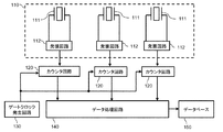
(センサーシステムの構成の概要)
図1に示すように、本実施形態におけるセンサーシステムは、水晶振動体111と発振回路112とを複数備えた振動子アレイ110、カウンタ回路120、ゲートクロック発生回路130、データ処理回路140、及びデータベース150を含んで構成される。
なお、振動子アレイ110は少なくとも複数の水晶振動体111を含めばよく、必ずしも発振回路112を含む必要はない。
(Summary of sensor system configuration)
As shown in FIG. 1, the sensor system according to the present embodiment includes a transducer array 110 including a plurality of
Note that the transducer array 110 may include at least a plurality of
(水晶振動体111)
水晶振動体111は、表面と裏面とに励振電極対が形成され、この励振電極対を介して発振回路112に接続されるよう構成されている。
(Quartz vibrator 111)
The
また、水晶振動体111の励振電極の表面には、特定の物質を選択的に吸着する特性を有する吸着膜を備えており、ニオイ検出の対象物質である周辺気体(又は液体その他の媒体)中に露出している。この吸着膜は、水晶振動体111毎に異なる膜が用いられ、図1においては、それぞれの水晶振動体111は異なる吸着膜を備えている。吸着膜は、水晶振動体111の両面に形成することが好ましい。
Further, the surface of the excitation electrode of the
また、吸着膜としては、ポリマー膜、脂質膜、たんぱく質膜、又は単分子膜のいずれかが用いられる。 In addition, as the adsorption film, a polymer film, a lipid film, a protein film, or a monomolecular film is used.
(発振回路112)
発振回路112は、水晶振動体111に接続されるよう構成される。この発振回路112は、前述の数式1で示される周波数をもつ発振信号を出力する回路である。発振回路112の具体的構成については後述する。
(Oscillation circuit 112)
The
(カウンタ回路120)
カウンタ回路120は、発振回路112から入力された発振信号と、ゲートクロック発生回路130から入力されたゲートクロックとの関係を特定し、カウント値としてデータ処理回路140へ出力するよう構成される。具体的には、カウンタ回路120は、ゲートクロックの1周期(以下、ゲート時間という)に、発振信号の立ち上がりエッジ又は立ち下がりエッジによって特定されるパルスがいくつ入るかをカウントする。
(Counter circuit 120)
The
(ゲートクロック発生回路130)
ゲートクロック発生回路130は、カウンタ回路120にゲートクロックを供給するよう構成される。すなわち、ゲートクロック発生回路130は所定の周波数を有するゲートクロックを生成する機能を有しており、この信号をそれぞれのカウンタ回路120へ送信する。なお、ゲートクロックは発振信号よりも低い周波数を持つ信号である。言い換えれば、ゲートクロックの信号周期は、発振信号よりも長くなっている。具体的には、ゲートクロックの信号周期は0.01μ秒以上1秒未満の時間にすることが好ましいことが経験則から分かっている。
(Gate clock generation circuit 130)
The gate
(データ処理回路140)
データ処理回路140は、複数のカウンタ回路120から出力されるカウント値に基づいて、それぞれの水晶振動体111が対象物質を吸着したか否かと、吸着した量と、のいずれか一方又は双方を特定するよう構成される。具体的には、それぞれのカウンタ回路120から出力されたカウント値に基づいて、対応する水晶振動体111と発振回路112とで生成した発振信号の周波数を特定する。さらにデータ処理回路140は、発振信号の周波数の時間変化を観測する。そして、データ処理回路140は、発振信号の周波数の変化に基づいて、それぞれの水晶振動体111が物質を吸着したか否か、吸着した場合はどれくらいの量を吸着したのかを、データベース150を参照することによって特定することができる。
(Data processing circuit 140)
Based on the count values output from the plurality of
(データベース150)
データベース150は、ニオイの特定に必要な情報を格納しており、データ処理回路140からの要求に応じて当該情報を送信するよう構成される。ここで、ニオイの特定の必要な情報とは、例えばそれぞれの水晶振動体111における発振信号の周波数変動と、それぞれの水晶振動体111の吸着の対象物質の吸着量との関係を示すテーブルなどである。
(Database 150)
The
(ニオイセンサーとしての動作)
まず、基準となる空気(好ましくは活性炭などで処理した無臭の空気)の下で複数の水晶振動体111を発振させ、それぞれの水晶振動体111に接続された発振回路112から出力される発振信号の周波数を計測する。
(Operation as an odor sensor)
First, a plurality of
次に、複数の水晶振動体111を対象物質である気体に暴露させる。ここで、気体にニオイがあれば、その気体中にはそのニオイを構成するニオイ分子が含まれており、そのニオイ分子が水晶振動体111の表面に形成された吸着膜に吸着される。このニオイ分子には質量があるため、ニオイ分子を吸着した吸着膜を有する水晶振動体111は、吸着したニオイ分子の質量に相当する負荷が増大し、この負荷の増大は発振信号の周波数の減少として観測される。つまり、カウンタ回路120及びデータ処理回路140によって、この発振信号の周波数の減少を特定し、ニオイ分子の吸着量を求めることができる。
Next, the plurality of
一方、データベース150には予めデータベース化された、発振信号の周波数の変化とニオイ分子の吸着量との関係、及びニオイ分子の吸着量とニオイとの関係が格納されている。データ処理回路140はこのデータベース150を参照することで、データベース150上に一致するデータが存在すれば、対象物質である気体が既知のニオイを有することを特定することが可能となる。
On the other hand, the
(2.振動体と接続された発振回路の構成例)
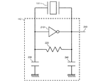
図2は、振動体111と接続された発振回路112の構成の一例を示す図である。図2に示すように、発振回路112は、インバーター210、帰還抵抗220、付加容量230、240、及び発振信号出力端子250を含む。発振回路112はさらに、水晶振動体111に接続されている。この水晶振動体111と発振回路112との組み合わせは、いわゆるコルピッツ発振回路を構成している。水晶振動体111の第1の励振電極は、インバーター210の入力、帰還抵抗220の第1の端子、及び付加容量230の第1の端子に接続されている。水晶振動体111の第2の励振電極は、インバーター210の出力、帰還抵抗220の第2の端子、付加容量240の第1の端子、及び発振信号出力端子250に接続されている。また、付加容量230の第2の端子及び付加容量240の第2の端子は、いずれも接地されている。なお、水晶振動体111及び帰還抵抗220の端子はいずれも極性を有するものではないため、端子を逆に接続しても動作に影響はない。
(2. Configuration example of oscillation circuit connected to vibrator)
FIG. 2 is a diagram illustrating an example of the configuration of the
なお、このコルピッツ発振回路はあくまで一例に過ぎず、これ以外の構成によって発振回路112を構成してもよい。
Note that this Colpitts oscillation circuit is merely an example, and the
(3.振動体の構成例)
次に、本実施形態の振動子アレイで使用する水晶振動体(水晶振動板)の構成について、さらに詳しく説明する。
(3. Configuration example of vibrator)
Next, the configuration of the crystal vibrating body (crystal vibrating plate) used in the vibrator array of this embodiment will be described in more detail.
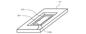
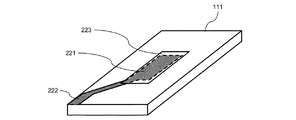
図3は、本実施形態における水晶振動体の表面の構成例を示す図、図4は本実施形態における水晶振動体の裏面の構成例を示す図である。
図3に示すように、水晶振動体111は表面に窪みを有する、いわゆる逆メサ型の振動体であり、表面には励振電極211、及び引き出し電極212を備える。さらに、特定の物質を選択的に吸着する特性を有する吸着膜213が、励振電極211を覆うように形成されている。また、図4に示すように、裏面には窪みは形成されていない。裏面には励振電極221、及び引き出し電極222を備え、励振電極221を覆うように、吸着膜223が形成されている。この吸着膜223は、表面に形成された吸着膜213と同じ物質を吸着する特性を有することが好ましいが、これに限るものではない。励振電極211及び221は、それぞれ表面及び裏面の中央部を含む領域に形成されている。この水晶振動体111はATカットの水晶振動体であり、水晶板の表裏に形成した励振電極間に電圧を印加するといわゆる厚みすべり振動モードで動作する。厚みすべり振動モードとは、振動体を構成する水晶の結晶格子が厚み方向にひずみ、表面と裏面とが交互に相異なる方向に変位することによって所定の周波数で振動するものである。以下、水晶振動体111の表面と裏面とに形成された励振電極211及び221を「励振電極対」と、引き出し電極212及び222を「引き出し電極対」と呼ぶ。
FIG. 3 is a diagram illustrating a configuration example of the front surface of the crystal resonator in the present embodiment, and FIG. 4 is a diagram illustrating a configuration example of the back surface of the crystal resonator in the present embodiment.
As shown in FIG. 3, the
励振電極対211及び221は、水晶振動体111の窪み部分に、水晶振動体111を挟み込むように形成されている。前述のように、この励振電極対211及び221に電圧を印加することで水晶振動体111が振動を開始する。
The
引き出し電極対212及び222それぞれは、水晶振動体111の少なくとも一端に接するように形成されている。この引き出し電極対212及び222は、水晶振動体111の表面と裏面とで、当該水晶振動体111の厚さ方向に重ならないように形成されることが好ましい。引き出し電極対212及び222が水晶振動体111の厚さ方向で重なってしまった場合、引き出し電極対の間でクロストークが発生してしまうことがあるので、これを避けるためである。
Each of the extraction electrode pairs 212 and 222 is formed so as to be in contact with at least one end of the
(4.基板上における振動体の設置例)
本発明は、上記のとおり説明したセンサーシステムなどに利用される振動子及び振動子アレイであるが、基板上における振動体の設置に大きな特徴がある。以下、振動子アレイの具体的構成について、例を挙げながら説明する。
(4. Example of installation of vibrator on substrate)
The present invention is a vibrator and a vibrator array used in the sensor system described above, but has a great feature in the placement of the vibrator on the substrate. Hereinafter, a specific configuration of the transducer array will be described with examples.
(1)実施形態1
図5は、本実施形態1での基板上における振動体の第1の設置例を示す模式的な側面図である。
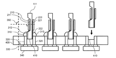
図5に示すように、基板300は複数の水晶振動体111を立設されて構成される。また、基板300は、第1の接続部310、貫通配線320、及び第2の接続部330を含んで構成される。さらに、基板300の裏面には集積回路340が配置されている。
(1)
FIG. 5 is a schematic side view illustrating a first installation example of the vibrating body on the substrate in the first embodiment.
As shown in FIG. 5, the
水晶振動体111の励振電極対211及び221は、それぞれ引き出し電極対212及び222と、第1の接続部310とを介して基板300の貫通配線320に接続されている。第1の接続部310は、基板300の表面に配置されており、上記のように水晶振動体111と基板300の貫通配線320とを接続するものである。貫通配線320は、基板300を貫通するよう構成されており、水晶振動体111と、基板300の裏面に配置された集積回路340とを接続するものである。貫通配線320は、基板300の裏面に配置された第2の接続部330を介して集積回路340と接続されている。集積回路340は発振回路112を含んで構成されている。なお、第1の接続部310及び第2の接続部330は、銀ペーストのような導電性ペーストで構成される。
The
このようにして、基板300には複数の水晶振動体111が立設され、複数の水晶振動体111は、基板300に含まれる第1の接続部310、貫通配線320、及び第2の接続部330を介して集積回路340に接続される。
In this way, a plurality of
また、水晶振動体111は、当該水晶振動体111の法線方向と基板の主たる面の法線方向とが所定の角度350を有するように、基板300に立設されている。本実施形態1においては、この所定の角度350は直角である。
In addition, the
以上のように、本実施形態1の振動子は、厚みすべり振動モードで振動する水晶振動体111と、水晶振動体111の第1の面(例えば表面)における、第1の領域に形成された第1の吸着膜213と、水晶振動体111の第1の面と対向する第2の面(例えば裏面)における、第2の領域に形成された第2の吸着膜223と、表面に水晶振動体111を立設された基板300と、を備え、水晶振動体111は、第1の面及び第2の面とは異なる第3の面(例えば立設面)において基板300に接していることを特徴とする。
As described above, the vibrator according to the first embodiment is formed in the first region of the
かかる構成によれば、水晶振動体111を基板300に立設することによって、水晶振動体111の両面に形成された吸着膜213及び223に対象物質を接触させやすくなり、吸着物質量ΔMを大きくすることができる。これにより、水晶振動体111による対象
物質の検出感度を高めることが可能となる。
According to such a configuration, by placing the
また、水晶振動体111の一辺のみが接するように基板300に立設して固定すれば、水晶振動体111へ及ぶ基板300の歪みなどによる応力の影響による発振周波数の変動を最小限に留めることができる。
Further, if the
また、本実施形態1の振動子における水晶振動体111は、表面又は裏面のいずれかの面に窪みを有する逆メサ型の構造であることが好ましい。
Moreover, it is preferable that the
かかる構成によれば、水晶振動体111の一方の面に窪みを有するいわゆる逆メサ構造の水晶振動体111を用いた場合でも、水晶振動体111の両面に対象物質を接触させやすくなり、吸着物質量ΔMを大きくすることができる。
According to such a configuration, even when the so-called inverted
なお、本実施形態1の振動子アレイは、少なくとも一方の面が窪みを有する、複数の水晶振動体111と、当該複数の水晶振動体111のそれぞれが立設された基板300とを備える、ということもできる。
The vibrator array according to the first embodiment includes a plurality of
また、第1の領域の、水晶振動体111と第1の吸着膜213との間に形成された励振電極211と、第2の領域の、水晶振動体111と第2の吸着膜223との間に形成された励振電極221と、をさらに備えることが好ましい。
In addition, the
かかる構成によれば、吸着膜213及び223を形成した領域の、水晶振動体111と吸着膜213及び223との間に、それぞれ励振電極211及び221を設けることによって、水晶振動体111をむらなく振動させることができる。
According to such a configuration, by providing the
なお、水晶振動体111における第1及び第2の領域を、それぞれ第1の面及び第2の面の中央部分を含むものとすることは、上記の水晶振動体111をさらにむらなく振動させることができるため、さらに好ましい。
It should be noted that the first and second regions of the
また、第1の面の、基板300と接しかつ第1の領域と重ならない第3の領域に形成された励振電極と、第2の面の、基板300と接しかつ第2の領域と重ならない第4の領域に形成された励振電極と、を備えることも好ましい。
In addition, the excitation electrode formed in the third region of the first surface that is in contact with the
また、上記いずれかの振動子を複数備え、振動子アレイを構成することが好ましい。
かかる構成の振動子アレイによれば、上記いずれかの振動子の特徴を生かしながら、複数の振動子を必要とする振動子アレイを構成することができ、例えば、対象物質の検出感度を高めた振動子アレイを構成することが可能となる。
なお、以下で説明する振動子を複数備えた振動子アレイを構成することも可能である。
Further, it is preferable that a plurality of any of the above-described vibrators are provided to constitute a vibrator array.
According to the transducer array having such a configuration, it is possible to configure a transducer array that requires a plurality of transducers while taking advantage of the characteristics of any of the transducers described above. For example, the detection sensitivity of the target substance is increased. An oscillator array can be configured.
It is also possible to configure a transducer array including a plurality of transducers described below.
また、本実施形態1の振動子、又は振動子アレイにおいては、水晶振動体111が、当該水晶振動体111の両面にそれぞれ形成された励振電極対211及び221と、当該水晶振動体111のそれぞれ両面に形成され、励振電極対211及び221にそれぞれ接続された引き出し電極対212及び222とを有し、当該引き出し電極対212及び222を介して水晶振動体111と基板300とが接続されていることが好ましい。
Further, in the vibrator or vibrator array according to the first embodiment, the
従来のように水晶振動体を基板の平面に実装する場合、水晶振動体の両面に形成された励振電極対と基板とを接続する際に、配線を引き回すなどの工夫が必要であった。本実施形態1の上記構成によれば、水晶振動体111を立設し、かつ引き出し電極対212及び222を介して基板300と水晶振動体111とを接続している。これにより、水晶振動体111の両面に形成された励振電極対211及び221と基板300との接続を容易にすることが可能となる。さらに、従来と比較して水晶振動体111と基板300との間の距離を短くすることが可能となる。これにより、かかる接続に銀ペーストなどの導電性ペーストを使用することができ、製造も容易になる。
When mounting a quartz oscillator on a plane of a substrate as in the prior art, it has been necessary to devise such as routing wiring when connecting the excitation electrode pair formed on both sides of the quartz oscillator and the substrate. According to the configuration of the first embodiment, the
また、基板300の裏面に取り付けられた、発振回路を含む集積回路340をさらに備え、励振電極対211及び221のそれぞれは、基板300を貫通する貫通配線320を介して集積回路340に接続されていることが好ましい。
Further, an
本実施形態1のかかる構成によれば、水晶振動体111と発振回路112との間の配線を短くすることができ、かかる配線に対するノイズの混入を減らすことができる。
According to such a configuration of the first embodiment, the wiring between the
本実施形態1においては水晶振動体111の法線方向と基板300の主たる面の法線方向との所定の角度350が直角である例を説明したが、この角度350は必ずしも直角である必要はない。ただし、例えば60度以上120度以下であることは好ましい。この場合、対象物質が水晶振動体111の両面に触れやすくなる。
In the first embodiment, the example in which the
また、第1の接続部310及び第2の接続部330は、銀ペーストのような導電性ペーストで構成されているため、配線で構成する場合と比較して製造しやすいという特徴がある。第1の接続部310及び第2の接続部330が銀ペーストで構成されることはより好ましく、この場合、当該接続部の電気抵抗を減らすことができ、かつ取り扱いが容易であるという特徴がある。
In addition, since the
また、この第1の接続部310及び第2の接続部330を構成する導電性ペーストを、樹脂などを用いて補強することがより好ましい。
It is more preferable to reinforce the conductive paste constituting the
ただし、第1の接続部310及び第2の接続部330は必ずしも導電性ペーストで構成されない場合であってもよい。この場合であっても、水晶振動体111による対象物質の検出感度を高めることは可能である。
However, the
なお、上記本実施形態1の特徴は、矛盾しない範囲で以下の実施形態においても共通である。 The features of the first embodiment are common to the following embodiments as long as they do not contradict each other.
(2)実施形態2
図6は、本実施形態2での基板上における振動体の第2の設置例を示す模式的な側面図である。実施形態2は実施形態1と多くの点で同一であるため、以下では相違点のみについて説明する。以下で具体的に説明しない点については、実施形態2と実施形態1とは同一の構成、機能を有する。
(2) Embodiment 2
FIG. 6 is a schematic side view illustrating a second installation example of the vibrating body on the substrate in the second embodiment. Since the second embodiment is the same as the first embodiment in many respects, only differences will be described below. The second embodiment and the first embodiment have the same configuration and function for points not specifically described below.
図6に示すように、基板400は溝410を有して構成される。水晶振動体111は、その一端が溝410に嵌め込まれるようにして、基板に立設されている。また、水晶振動体111は、溝410に嵌め込まれる側の一端における平坦部分が、反対側の端における平坦部分よりも長くなるよう構成されている。なお、平坦部分とは、水晶振動体111のうち、表面に窪みが形成されていない部分を指す。また、水晶振動体111の溝410に嵌め込まれる側の一端には、引き出し電極対212及び222が形成されている。
As shown in FIG. 6, the
以上のように、本実施形態2の振動子は、実施形態1の構成に加え、水晶振動体111が、基板400に設けられた溝410に嵌め込まれていることをさらなる特徴とする。
As described above, in addition to the configuration of the first embodiment, the vibrator according to the second embodiment is further characterized in that the
かかる特徴によれば、基板400上に立設させた水晶振動体111の取付け強度を高めることができる。これによって、振動や衝撃を受けたとしても、水晶振動体111が基板400から外れたり、水晶振動体111が破壊されたりする危険性を低くすることができる。また、第1の接続部310及び第2の接続部330に使用される導電性ペーストの量を減らしても十分な取付け強度が得られるため、製造コストを下げることもできる。
According to this feature, it is possible to increase the attachment strength of the
また、本実施形態2の振動子アレイは、基板400が溝410を有しており、当該溝410に水晶振動体111の一端が嵌め込まれるようにして、水晶振動体111が立設されていることをさらなる特徴ともいうことができる。
Further, in the vibrator array according to the second embodiment, the
さらに、本実施形態2の振動子アレイは、水晶振動体111の一端における平坦部分の長さが、水晶振動体111の一端と反対の他の端における平坦部分の長さよりも長いことを、さらなる特徴とする。
Further, in the vibrator array of the second embodiment, the length of the flat portion at one end of the
かかる特徴によれば、水晶振動体111における基板400に設けられた溝410に嵌め込まれる側の一端を他の端より長くしたため、基板400上に立設された水晶振動体111の取付け強度をさらに高めることができる。また、基板400に水晶振動体111を取り付けることを容易にすることもできる。
According to this feature, since one end of the
なお、本実施形態2では第1の接続部310を備える例を挙げて説明したが、第1の接続部310は必ずしも必要ではない。すなわち、溝410に貫通配線320が露出されており、水晶振動体111が溝410に嵌め込まれることで、引き出し電極対211及び221が、それぞれ対応する貫通配線320と接続されるように構成することもできる。
In the second embodiment, the example in which the
(3)実施形態3
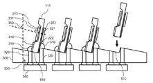
図7は、本実施形態3での基板上における振動体の第3の設置例を示す模式的な側面図である。実施形態3は実施形態1と多くの点で同一であるため、以下では相違点のみについて説明する。以下で具体的に説明しない点については、実施形態3と実施形態1とは同一の構成、機能を有する。
(3) Embodiment 3
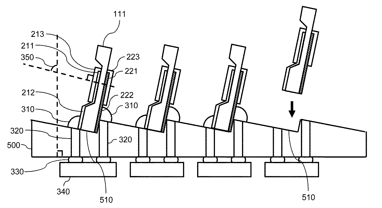
FIG. 7 is a schematic side view showing a third installation example of the vibrating body on the substrate in the third embodiment. Since the third embodiment is the same as the first embodiment in many respects, only differences will be described below. For points not specifically described below, the third embodiment and the first embodiment have the same configuration and function.
図7に示すように、基板500は、少なくとも複数の水晶振動体111が立設されている部分について傾斜面510を有するよう構成される。複数の水晶振動体111は、この傾斜面510の上に立設されるため、基板500の上に、所定の傾きを持つように設置される。言い換えると、複数の水晶振動体111は、それぞれの水晶振動体111の法線方向と基板500の主たる面の法線方向とがなす角度350が、所定の角度を有するよう基板500に立設されている。ここで、所定の角度は60度以上120度以下であることが好ましい。
As shown in FIG. 7, the
また、基板500は傾斜を持った階段構造になっており、水晶振動体111を立設する立設面である傾斜面510に対して、階段構造の段差面がほぼ垂直になるよう構成されている。このような基板500の構成によれば、階段構造における段差面と、立設面である傾斜面510とからなる角部に、水晶振動体111の角部を嵌め込むように立設することが可能である。この場合、水晶振動体111のうち、傾斜面510と接する部分よりも窪み部分に近い部分において、水晶振動体111の裏面の引き出し電極221と基板500の貫通配線320とを接続することができる。よって、本実施形態3における水晶振動体111の裏面の引き出し電極221は、傾斜面510と接する部分まで伸びている必要がなく、上記のとおり貫通配線320と接続可能な部分まで伸びていればよい。
In addition, the
また、基板500の貫通配線320が段差面に露出されるように形成することができる。この場合、水晶振動体111の裏面の引き出し電極221は、第1の接続部310を介さずに貫通配線320に接続することができる。
Further, the through
以上のように、本実施形態3の振動子は、実施形態1の構成に加え、水晶振動体111が、基板500に設けられた傾斜面510に立設されていることをさらなる特徴とする。
As described above, in addition to the configuration of the first embodiment, the resonator according to the third embodiment is further characterized in that the
かかる特徴によれば、基板500に対して傾斜角を持つように水晶振動体111を立設することができる。また、基板500に溝410を形成することなく傾斜面510を形成するので、溝410を形成するよりも容易に、水晶振動体111の取り付け強度を高めた基板500、及び基板500を含んだ振動子を製造することができる。
According to this feature, the
また、上記の特徴に加え、本実施形態3の振動子アレイにおける複数の水晶振動体111は、当該水晶振動体111の法線方向と基板500の主たる面の法線方向とがなす角度350が、60度以上120度以下になるよう前記基板に立設されていることをさらなる特徴とする。
In addition to the above features, the plurality of
水晶振動体111が基板500に対して過度に鋭角に立設された場合、水晶振動体111の近傍において気体などの吸着の対象物質が滞留してしまうことがある。この場合、水晶振動体111に触れる対象物質がリフレッシュされづらい状態になってしまい、水晶振動体111が所望の対象物質を適切に吸着することができなくなるおそれがある。
When the
本実施形態3の上記構成によれば、水晶振動体111の近傍で気体などの対象物質が滞留することを避けることができ、水晶振動体111が所望の対象物質を適切に吸着することができる。また、吸着膜を形成した水晶振動体111の両面にほぼ均等に対象物質が触れることとなり、効果的に対象物質を吸着することができる。
According to the configuration of the third embodiment, it is possible to avoid the retention of a target substance such as gas in the vicinity of the
なお、当該水晶振動体111の法線方向と基板500の主たる面の法線方向とがなす角度が、80度以上100度以下になるよう基板500に立設されていることがさらに好ましい。
It is further preferable that the
(5.振動体の配置例)
次に、本実施形態における複数の振動体の配置例について、具体的な例を挙げながら説明する。なお、以下で説明する図面は、振動子アレイを基板上部から見た図面である。
(5. Example of arrangement of vibrators)
Next, an arrangement example of a plurality of vibrating bodies in the present embodiment will be described with a specific example. The drawings described below are views of the transducer array as viewed from above the substrate.
(1)実施形態4
図8は、本実施形態4での基板上における振動体の第1の配置を基板上方から見た平面図である。
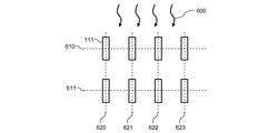
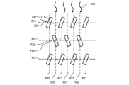
図8に示すように、基板には複数の水晶振動体111が立設して配置されている。図8に示される水晶振動体111は、いずれも基板に対して垂直に立設されたものの上面を示す。また、図8において、水晶振動体111で吸着する対象物質である気体、液体などの媒体は、流動方向600で示す方向に流動する。さらに、水晶振動体111は、基板上の第1の行610及び第2の行611と、第1乃至第4の列620乃至623との交点にその中心がくるように整列して配置されている。言い換えれば、複数の水晶振動体111は、第1の方向(行方向)、及び第1の方向に垂直な第2の方向(列方向)に並ぶように基板に連設されている。
(1) Embodiment 4
FIG. 8 is a plan view of the first arrangement of the vibrators on the substrate in the fourth embodiment as viewed from above the substrate.
As shown in FIG. 8, a plurality of
本実施形態4のように水晶振動体111を配置することにより、平面視において複数の水晶振動体111がマトリクス状に配置され、水晶振動体111の近傍において対象物質が流動しやすくなるため、リフレッシュされた対象物質が水晶振動体111に供給されるようにすることができる。
By arranging the
(2)実施形態5
図9は、本実施形態5での基板上における振動体の第2の配置を基板上方から見た平面図である。実施形態5は実施形態4と類似しているため、以下では相違点のみについて説明する。以下で具体的に説明しない点については、実施形態5と実施形態4とは同一の構成、機能を有する。
(2) Embodiment 5
FIG. 9 is a plan view of the second arrangement of the vibrating bodies on the substrate in the fifth embodiment as viewed from above the substrate. Since the fifth embodiment is similar to the fourth embodiment, only the differences will be described below. For points not specifically described below, the fifth and fourth embodiments have the same configuration and function.
図9に示すように、水晶振動体111は、基板上の第1乃至第3の行610乃至612の直線上に配置される。そして、奇数行においては第1乃至第4の列620乃至623と奇数行610又は612との交点に中心がくるように、水晶振動体111が整列して配置されている。また、偶数行においては、第1乃至第4の列620乃至623の間にそれぞれ均等間隔で描かれた第5乃至第7の列630乃至632と、偶数行611との交点に中心がくるように、水晶振動体111が整列して配置されている。
As shown in FIG. 9, the
図9では、奇数行と偶数行とがそれぞれグループとなって、それぞれのグループで同じ列上に中心がくるように水晶振動体111を配置した例を示したが、必ずしも奇数行と偶数行とでグループ分けする必要はない。すなわち、列方向に隣り合う行に配置された水晶振動体111は、並びがずれていればよい。
FIG. 9 shows an example in which the
すなわち、上記配置を言い換えれば、複数の水晶振動体111は、第1の方向(行方向)への並びが当該第1の方向と垂直な第2の方向(列方向)に複数行存在するように前記基板上に連設されており、隣り合う行間では、並びがずれるように配置されている。
In other words, in other words, the plurality of
上記本実施形態5の構成によれば、平面視においてマトリクス状に配置された複数の水晶振動体111が一列ごとにずれているので、水晶振動体111の近傍において対象物質が流動しやすく、かつ水晶振動体111に対象物質が触れやすいように、各水晶振動体111が配置されている。このように各水晶振動体111が配置されることにより、各水晶振動体111に触れる対象物質が常時リフレッシュされ、かつ水晶振動体111が吸着する対象媒体の量が多くなる。これにより、水晶振動体111が対象物質を吸着しやすくなり、また水晶振動体111の検出感度を高くすることができる。
According to the configuration of the fifth embodiment, since the plurality of
(3)実施形態6
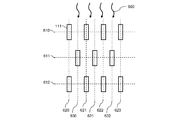
図10は、本実施形態6での基板上における振動体の第3の配置を基板上方から見た平面図である。実施形態6は実施形態5と類似しているため、以下では相違点のみについて説明する。以下で具体的に説明しない点については、実施形態6と実施形態5及び実施形態4とは同一の構成、機能を有する。
(3) Embodiment 6
FIG. 10 is a plan view of the third arrangement of the vibrators on the substrate in the sixth embodiment as viewed from above the substrate. Since the sixth embodiment is similar to the fifth embodiment, only the differences will be described below. For points not specifically described below, the sixth embodiment, the fifth embodiment, and the fourth embodiment have the same configuration and function.
図10に示すように、水晶振動体111は、その中心が実施形態5と同様になるよう配置されている。すなわち、複数の水晶振動体111は、第1の方向(行方向)への並びが当該第1の方向と垂直な第2の方向(列方向)に複数列存在するように前記基板上に連設されており、隣り合う列間では、並びがずれるように配置されている。ただし、本実施形態6ではさらに、隣り合う列間では、それぞれの水晶振動体111の法線方向700及び710が異なるように配置されている。より具体的には、奇数行610に配置された水晶振動体111の法線方向700は、行610方向の直線に対して第1の角度720を有している。一方で偶数行611に配置された水晶振動体111の法線方向710は、行611方向の直線に対して第2の角度730を有している。
As shown in FIG. 10, the
すなわち、上記配置を言い換えれば、複数の水晶振動体111は、第1の方向(行方向)への並びが第1の方向と垂直な第2の方向(列方向)に複数行存在するように基板に連設されており、隣り合う行間では、それぞれの水晶振動体111の法線方向700及び710が異なるように配置されている。
In other words, in other words, the plurality of
上記本実施形態6の構成によれば、平面視においてマトリクス状に配置された複数の水晶振動体111の各々が、互いに異なる方向を向いて配置されるので、水晶振動体111の間を流動する対象物質に乱流を生じさせることができ、さらに対象物質が水晶振動体111に触れやすくなる。これにより、水晶振動体111の検出感度をさらに高くすることができる。
According to the configuration of the sixth embodiment, each of the plurality of
なお、水晶振動体111の法線方向700が行610方向の直線に対して有する第1の角度720、及び法線方向710が行611方向の直線に対して有する第2の角度730は、45度以下にすることが好ましい。これらの角度を45度以下にすることで、水晶振動体111が吸着する対象物質の流動を妨げないようにしつつ、上記本実施形態6の特徴を生かすことができる。
The
(6.まとめ)
以上、本発明の実施形態について説明した。
(6. Summary)
The embodiment of the present invention has been described above.
本発明はさらに、上記説明した振動子、又は振動子アレイを使用した様々な電子機器を含む。 The present invention further includes various electronic devices using the vibrator or the vibrator array described above.
図11は、上記電子機器としての一例である、振動子アレイを使用したガス警報器についての構成例を示す図である。図11において、ガス警報器は、ニオイセンサー800、警報器810、及びスピーカー820を含んで構成される。
FIG. 11 is a diagram illustrating a configuration example of a gas alarm device using a transducer array, which is an example of the electronic device. In FIG. 11, the gas alarm device includes an
ニオイセンサー800は、図1に示した、振動子アレイを含むセンサーシステムであり、振動子アレイに含まれる水晶振動体は、検出対象となるガスが有するニオイ成分を吸着するための吸着膜を備える。ニオイセンサー800は、検出対象となるガスが有するニオイ成分が一定以上の量であると検出すると、警報器810に警報するよう指示する。警報器810は、ニオイセンサー800から指示に対応して、スピーカー820に警報するための音声信号を送信する。スピーカー820は、警報器810からの音声振動に基づいて警報を発する。なお、警報器810及びスピーカー820は従来技術を適用可能である。
The
かかる構成の電子機器は、上記説明したそれぞれの本発明の特徴を有しているため、例えば、振動体の検出感度を高めることなどが可能となる。 Since the electronic apparatus having such a configuration has the above-described features of the present invention, for example, the detection sensitivity of the vibrating body can be increased.
なお、本発明は、上記実施形態に限定されることなく、それぞれの実施形態を互いに組み合わせたり、種々に変形したりして適用することが可能である。例えば、本発明は、図7のように水晶振動体111が立設されている基板部分について傾斜面を備えながら、図9のように複数の水晶振動体111を配置することなどを含む。
In addition, this invention is not limited to the said embodiment, It is possible to apply each embodiment combining each other or changing it variously. For example, the present invention includes disposing a plurality of
本発明の振動子、及び振動子アレイは、例えばセンサーシステムに使用可能であり、ニオイセンサー、アルコールセンサー、又は麻薬探知機など、広範な機器に使用可能である。 The vibrator and the vibrator array of the present invention can be used for a sensor system, for example, and can be used for a wide range of devices such as an odor sensor, an alcohol sensor, or a drug detector.
110…振動子アレイ、111…水晶振動体、112…発振回路、120…カウンタ回路、130…ゲートクロック発生回路、140…データ処理回路、150…データベース、210…インバーター、211…励振電極、212…電極、213…吸着膜、220…帰還抵抗、221…励振電極、222…電極、223…吸着膜、230…付加容量、240…付加容量、250…発振信号出力端子、300…基板、310…接続部、320…貫通配線、330…接続部、340…集積回路、350…角度、400…基板、410…溝、500…基板、510…傾斜面、600…流動方向、800…ニオイセンサー、810…警報器、820…スピーカー
DESCRIPTION OF SYMBOLS 110 ... Vibrator array, 111 ... Crystal oscillator, 112 ... Oscillator circuit, 120 ... Counter circuit, 130 ... Gate clock generation circuit, 140 ... Data processing circuit, 150 ... Database, 210 ... Inverter, 211 ... Excitation electrode, 212 ... Electrode, 213 ... adsorption film, 220 ... feedback resistor, 221 ... excitation electrode, 222 ... electrode, 223 ... adsorption film, 230 ... addition capacitor, 240 ... addition capacitor, 250 ... oscillation signal output terminal, 300 ... substrate, 310 ...
Claims (8)
前記振動体の第1の面における、第1の領域に形成された第1の吸着膜と、
前記振動体の前記第1の面と対向する第2の面における、第2の領域に形成された第2の吸着膜と、
表面に前記振動体を立設された基板と、を備え、
前記振動体は、前記基板に設けられた傾斜面に立設されて前記第1の面及び前記第2の面とは異なる第3の面において前記基板に接している
ことを特徴とする振動子。 A vibrating body that vibrates in a thickness-shear vibration mode;
A first adsorption film formed in a first region on the first surface of the vibrator;
A second adsorption film formed in a second region on a second surface opposite to the first surface of the vibrator;
A substrate on which the vibrating body is erected, and
The vibrator is erected on an inclined surface provided on the substrate and is in contact with the substrate on a third surface different from the first surface and the second surface. .
前記第2の領域の、前記振動体と前記第2の吸着膜との間に形成された第2の電極と、
をさらに備える
ことを特徴とする請求項1に記載の振動子。 A first electrode formed between the vibrating body and the first adsorption film in the first region;
A second electrode formed between the vibrating body and the second adsorption film in the second region;
The vibrator according to claim 1, further comprising:
前記第2の面の、前記基板と接しかつ前記第2の領域と重ならない第4の領域に形成された第2の電極と、をさらに備える
ことを特徴とする請求項1に記載の振動子。 A first electrode formed in a third region of the first surface in contact with the substrate and not overlapping the first region;
The vibrator according to claim 1, further comprising: a second electrode formed in a fourth region of the second surface that is in contact with the substrate and does not overlap the second region. .
前記第1の電極及び前記第2の電極のそれぞれは、前記基板を貫通する配線を介して前記集積回路に接続されている
ことを特徴とする請求項2又は3のいずれか1項に記載の振動子。 An integrated circuit including an oscillation circuit attached to the back surface of the substrate;
4. The device according to claim 2, wherein each of the first electrode and the second electrode is connected to the integrated circuit through a wiring penetrating the substrate. 5. Vibrator.
ことを特徴とする請求項1乃至4のいずれか1項に記載の振動子。 The vibrator according to any one of claims 1 to 4 , wherein the vibrating body has an inverted mesa structure having a depression on any surface.
ことを特徴とする請求項6に記載の振動子アレイ。 The plurality of vibrators are connected to the substrate so that a plurality of vibrators are arranged in a first direction in a second direction perpendicular to the first direction, and between adjacent rows, The vibrator array according to claim 6 , wherein the vibrators are arranged so that normal directions with respect to the first surface or the second surface of the vibrator are different.
Priority Applications (2)
| Application Number | Priority Date | Filing Date | Title |
|---|---|---|---|
| JP2009112011A JP4737726B2 (en) | 2009-05-01 | 2009-05-01 | Vibrator, vibrator array, and electronic device |
| US12/769,091 US8247948B2 (en) | 2009-05-01 | 2010-04-28 | Oscillator, oscillator array and an electronic apparatus |
Applications Claiming Priority (1)
| Application Number | Priority Date | Filing Date | Title |
|---|---|---|---|
| JP2009112011A JP4737726B2 (en) | 2009-05-01 | 2009-05-01 | Vibrator, vibrator array, and electronic device |
Related Child Applications (1)
| Application Number | Title | Priority Date | Filing Date |
|---|---|---|---|
| JP2011028484A Division JP5435243B2 (en) | 2011-02-14 | 2011-02-14 | Vibrator and electronic equipment |
Publications (2)
| Publication Number | Publication Date |
|---|---|
| JP2010263365A JP2010263365A (en) | 2010-11-18 |
| JP4737726B2 true JP4737726B2 (en) | 2011-08-03 |
Family
ID=43029944
Family Applications (1)
| Application Number | Title | Priority Date | Filing Date |
|---|---|---|---|
| JP2009112011A Expired - Fee Related JP4737726B2 (en) | 2009-05-01 | 2009-05-01 | Vibrator, vibrator array, and electronic device |
Country Status (2)
| Country | Link |
|---|---|
| US (1) | US8247948B2 (en) |
| JP (1) | JP4737726B2 (en) |
Cited By (1)
| Publication number | Priority date | Publication date | Assignee | Title |
|---|---|---|---|---|
| US10422771B2 (en) | 2014-08-29 | 2019-09-24 | Kabushikigaisha Aroma Bit, Inc. | Odor detection system, odor identification device, and odor identification method |
Families Citing this family (7)
| Publication number | Priority date | Publication date | Assignee | Title |
|---|---|---|---|---|
| JP4737726B2 (en) * | 2009-05-01 | 2011-08-03 | セイコーエプソン株式会社 | Vibrator, vibrator array, and electronic device |
| JP5641296B2 (en) * | 2010-06-16 | 2014-12-17 | セイコーエプソン株式会社 | Frequency measuring device, odor sensor and electronic device equipped with the same |
| CN202535316U (en) | 2011-03-09 | 2012-11-14 | 精工爱普生株式会社 | Vibrating element, vibrator, oscillator and electronic equipment |
| JP5708089B2 (en) * | 2011-03-18 | 2015-04-30 | セイコーエプソン株式会社 | Piezoelectric vibration element, piezoelectric vibrator, piezoelectric oscillator, and electronic device |
| US10528195B2 (en) * | 2014-04-30 | 2020-01-07 | Lg Innotek Co., Ltd. | Touch device, wearable device having the same and touch recognition method |
| JP6390836B2 (en) | 2014-07-31 | 2018-09-19 | セイコーエプソン株式会社 | Vibrating piece, vibrator, vibrating device, oscillator, electronic device, and moving object |
| WO2023175956A1 (en) * | 2022-03-18 | 2023-09-21 | I-Pex株式会社 | Substance detecting system |
Family Cites Families (24)
| Publication number | Priority date | Publication date | Assignee | Title |
|---|---|---|---|---|
| JPS543486A (en) * | 1977-06-09 | 1979-01-11 | Citizen Watch Co Ltd | Structure of crystal oscillator |
| US4523120A (en) * | 1984-06-04 | 1985-06-11 | The United States Of America As Represented By The Secretary Of The Navy | Precise bearing support ditherer with piezoelectric drive means |
| JP2816550B2 (en) | 1987-03-11 | 1998-10-27 | 相互薬工株式会社 | How to detect bitter or odorous substances |
| WO1991012663A1 (en) * | 1990-02-09 | 1991-08-22 | Toyo Communication Equipment Co., Ltd. | Structure for holding ultrathin plate piezoelectric resonator in package |
| JPH03282232A (en) * | 1990-03-30 | 1991-12-12 | Toshiba Corp | Odor detecting apparatus |
| US5894651A (en) * | 1990-10-29 | 1999-04-20 | Trw Inc. | Method for encapsulating a ceramic device for embedding in composite structures |
| JPH0812141B2 (en) | 1991-12-16 | 1996-02-07 | 日本電信電話株式会社 | Gas discrimination method |
| JPH05187986A (en) | 1992-01-09 | 1993-07-27 | Nippon Telegr & Teleph Corp <Ntt> | Odor sensing system |
| JPH06104641A (en) * | 1992-09-22 | 1994-04-15 | Nikko Electron Kk | Surface mount type oscillator |
| JPH0727731A (en) * | 1993-07-14 | 1995-01-31 | Oki Electric Ind Co Ltd | Odor sensor and odor sensor unit |
| JPH1141059A (en) * | 1997-07-16 | 1999-02-12 | Daishinku Co | Crystal oscillator |
| JP4061714B2 (en) * | 1998-06-24 | 2008-03-19 | エプソントヨコム株式会社 | Piezoelectric oscillator and manufacturing method thereof |
| JP4442965B2 (en) * | 1999-11-01 | 2010-03-31 | セイコーインスツル株式会社 | Ultrasonic motor and electronic device with ultrasonic motor |
| JP3826665B2 (en) * | 2000-04-18 | 2006-09-27 | セイコーエプソン株式会社 | Quartz vibrating piece, method for manufacturing quartz vibrating piece, and quartz device |
| JP2003318699A (en) * | 2002-04-23 | 2003-11-07 | Piedekku Gijutsu Kenkyusho:Kk | Crystal unit and its manufacturing method |
| JP2004361269A (en) * | 2003-06-05 | 2004-12-24 | Canon Inc | Multi-channel sensor and its manufacturing method, biosensor system and its manufacturing method |
| JP4890911B2 (en) * | 2006-03-31 | 2012-03-07 | 京セラキンセキ株式会社 | QCM sensor element |
| CN101512787B (en) * | 2006-09-08 | 2010-11-10 | 柯尼卡美能达控股株式会社 | Shear mode piezoelectric actuator and droplet discharge head |
| JP4432990B2 (en) * | 2007-03-22 | 2010-03-17 | セイコーエプソン株式会社 | Sensor and electronic equipment |
| US7471032B1 (en) * | 2007-06-05 | 2008-12-30 | Texas Instruments Incorporated | Shock resistant and mode mixing resistant torsional hinged device |
| JP2009222669A (en) | 2008-03-18 | 2009-10-01 | Seiko Epson Corp | Mass measuring apparatus |
| JP4737726B2 (en) * | 2009-05-01 | 2011-08-03 | セイコーエプソン株式会社 | Vibrator, vibrator array, and electronic device |
| JP5582447B2 (en) * | 2009-08-27 | 2014-09-03 | セイコーエプソン株式会社 | Electric circuit, sensor system including the electric circuit, and sensor device including the electric circuit |
| JP5435243B2 (en) * | 2011-02-14 | 2014-03-05 | セイコーエプソン株式会社 | Vibrator and electronic equipment |
-
2009
- 2009-05-01 JP JP2009112011A patent/JP4737726B2/en not_active Expired - Fee Related
-
2010
- 2010-04-28 US US12/769,091 patent/US8247948B2/en active Active
Cited By (3)
| Publication number | Priority date | Publication date | Assignee | Title |
|---|---|---|---|---|
| US10422771B2 (en) | 2014-08-29 | 2019-09-24 | Kabushikigaisha Aroma Bit, Inc. | Odor detection system, odor identification device, and odor identification method |
| US11112383B2 (en) | 2014-08-29 | 2021-09-07 | Kabushikigaisha Aroma Bit, Inc. | Odor detection system, odor identification device, and odor identification method |
| US11946904B2 (en) | 2014-08-29 | 2024-04-02 | Kabushikigaisha Aroma Bit, Inc. | Sample information acquisition unit, information processing unit, odor identification device |
Also Published As
| Publication number | Publication date |
|---|---|
| US20100277251A1 (en) | 2010-11-04 |
| JP2010263365A (en) | 2010-11-18 |
| US8247948B2 (en) | 2012-08-21 |
Similar Documents
| Publication | Publication Date | Title |
|---|---|---|
| JP5435243B2 (en) | Vibrator and electronic equipment | |
| JP4737726B2 (en) | Vibrator, vibrator array, and electronic device | |
| JP4757026B2 (en) | Acceleration sensor characteristic adjustment method | |
| CN102209890B (en) | Detection sensor and detection sensor transducer | |
| KR102303896B1 (en) | material detection element | |
| JP2001343240A (en) | Capacitance-type outer force-detecting device | |
| JPWO2005012921A1 (en) | Acceleration sensor | |
| JP3446732B2 (en) | Acceleration sensor | |
| JP4840621B2 (en) | Oscillation circuit, oscillation circuit group, electronic device, and layout method of oscillation circuit group | |
| JP5093405B2 (en) | Vibrating gyro element | |
| JP2002107373A (en) | Acceleration sensor | |
| TWI820185B (en) | Substance detection components | |
| JP2996137B2 (en) | Vibrating gyro | |
| CN101900658B (en) | Quartz sensor and sensing device | |
| US7091451B2 (en) | Heating element induction of time-varying thermal gradient in elongated beam to cause one or more elongated beam oscillations | |
| JP2009222669A (en) | Mass measuring apparatus | |
| JP2004150879A (en) | Cell for biosensor | |
| JP5321812B2 (en) | Physical quantity sensor and physical quantity measuring device | |
| JP2013221896A (en) | Sensitive sensor and sensitive instrument | |
| JP2000275126A (en) | Force sensor circuit | |
| JP3371609B2 (en) | Vibrating gyro | |
| JP2011112436A (en) | Liquid detection sensor | |
| JPH0914966A (en) | Vibrational gyro | |
| JP2001082961A (en) | Angular velocity sensor and method of manufacturing angular velocity sensor | |
| JP2009229353A (en) | Device and system for sensing gas |
Legal Events
| Date | Code | Title | Description |
|---|---|---|---|
| A131 | Notification of reasons for refusal |
Free format text: JAPANESE INTERMEDIATE CODE: A131 Effective date: 20101213 |
|
| A521 | Request for written amendment filed |
Free format text: JAPANESE INTERMEDIATE CODE: A523 Effective date: 20110214 |
|
| A01 | Written decision to grant a patent or to grant a registration (utility model) |
Free format text: JAPANESE INTERMEDIATE CODE: A01 Effective date: 20110411 |
|
| R150 | Certificate of patent or registration of utility model |
Free format text: JAPANESE INTERMEDIATE CODE: R150 |
|
| A61 | First payment of annual fees (during grant procedure) |
Free format text: JAPANESE INTERMEDIATE CODE: A61 Effective date: 20110424 |
|
| FPAY | Renewal fee payment (event date is renewal date of database) |
Free format text: PAYMENT UNTIL: 20140513 Year of fee payment: 3 |
|
| S531 | Written request for registration of change of domicile |
Free format text: JAPANESE INTERMEDIATE CODE: R313531 |
|
| R350 | Written notification of registration of transfer |
Free format text: JAPANESE INTERMEDIATE CODE: R350 |
|
| LAPS | Cancellation because of no payment of annual fees |