JP4732201B2 - Sensing device using electromagnetic waves - Google Patents
Sensing device using electromagnetic waves Download PDFInfo
- Publication number
- JP4732201B2 JP4732201B2 JP2006073612A JP2006073612A JP4732201B2 JP 4732201 B2 JP4732201 B2 JP 4732201B2 JP 2006073612 A JP2006073612 A JP 2006073612A JP 2006073612 A JP2006073612 A JP 2006073612A JP 4732201 B2 JP4732201 B2 JP 4732201B2
- Authority
- JP
- Japan
- Prior art keywords
- electromagnetic wave
- transmission path
- specimen
- bent portion
- terahertz wave
- Prior art date
- Legal status (The legal status is an assumption and is not a legal conclusion. Google has not performed a legal analysis and makes no representation as to the accuracy of the status listed.)
- Expired - Fee Related
Links
- 230000005540 biological transmission Effects 0.000 claims description 119
- 239000011248 coating agent Substances 0.000 claims description 22
- 238000000576 coating method Methods 0.000 claims description 22
- 230000003993 interaction Effects 0.000 claims description 22
- 238000005452 bending Methods 0.000 claims description 21
- 230000001902 propagating effect Effects 0.000 claims description 20
- 238000001514 detection method Methods 0.000 claims description 17
- 125000006850 spacer group Chemical group 0.000 claims description 10
- 239000002184 metal Substances 0.000 claims description 8
- 229910052751 metal Inorganic materials 0.000 claims description 8
- 230000000644 propagated effect Effects 0.000 claims description 5
- 230000008859 change Effects 0.000 claims description 4
- 238000009826 distribution Methods 0.000 claims description 4
- 230000005684 electric field Effects 0.000 claims description 4
- 239000012491 analyte Substances 0.000 claims description 2
- 238000000034 method Methods 0.000 description 21
- 230000000694 effects Effects 0.000 description 7
- 238000003384 imaging method Methods 0.000 description 7
- 239000012298 atmosphere Substances 0.000 description 6
- 238000005516 engineering process Methods 0.000 description 5
- 238000004458 analytical method Methods 0.000 description 4
- 239000006185 dispersion Substances 0.000 description 4
- 230000005672 electromagnetic field Effects 0.000 description 4
- 230000007246 mechanism Effects 0.000 description 4
- 230000003287 optical effect Effects 0.000 description 4
- 230000008569 process Effects 0.000 description 4
- 239000010410 layer Substances 0.000 description 3
- 239000000463 material Substances 0.000 description 3
- 238000005259 measurement Methods 0.000 description 3
- 239000013307 optical fiber Substances 0.000 description 3
- XLYOFNOQVPJJNP-UHFFFAOYSA-N water Substances O XLYOFNOQVPJJNP-UHFFFAOYSA-N 0.000 description 3
- 229910001218 Gallium arsenide Inorganic materials 0.000 description 2
- 238000000862 absorption spectrum Methods 0.000 description 2
- 150000001875 compounds Chemical class 0.000 description 2
- 239000012792 core layer Substances 0.000 description 2
- 238000010586 diagram Methods 0.000 description 2
- 239000011347 resin Substances 0.000 description 2
- 229920005989 resin Polymers 0.000 description 2
- 239000004065 semiconductor Substances 0.000 description 2
- 239000000758 substrate Substances 0.000 description 2
- RYGMFSIKBFXOCR-UHFFFAOYSA-N Copper Chemical compound [Cu] RYGMFSIKBFXOCR-UHFFFAOYSA-N 0.000 description 1
- 238000005253 cladding Methods 0.000 description 1
- 238000004891 communication Methods 0.000 description 1
- 239000004020 conductor Substances 0.000 description 1
- 230000008878 coupling Effects 0.000 description 1
- 238000010168 coupling process Methods 0.000 description 1
- 238000005859 coupling reaction Methods 0.000 description 1
- 239000013078 crystal Substances 0.000 description 1
- 238000000151 deposition Methods 0.000 description 1
- 238000011161 development Methods 0.000 description 1
- 239000003989 dielectric material Substances 0.000 description 1
- 238000005530 etching Methods 0.000 description 1
- 238000007689 inspection Methods 0.000 description 1
- 230000001678 irradiating effect Effects 0.000 description 1
- 239000007788 liquid Substances 0.000 description 1
- 238000004519 manufacturing process Methods 0.000 description 1
- 239000012299 nitrogen atmosphere Substances 0.000 description 1
- 230000000737 periodic effect Effects 0.000 description 1
- 238000000206 photolithography Methods 0.000 description 1
- 239000004038 photonic crystal Substances 0.000 description 1
- 230000000704 physical effect Effects 0.000 description 1
- 238000012545 processing Methods 0.000 description 1
- 230000035945 sensitivity Effects 0.000 description 1
- 238000004611 spectroscopical analysis Methods 0.000 description 1
- 238000004528 spin coating Methods 0.000 description 1
- 238000003892 spreading Methods 0.000 description 1
- 230000007480 spreading Effects 0.000 description 1
- 239000000126 substance Substances 0.000 description 1
- 238000005211 surface analysis Methods 0.000 description 1
- 230000001360 synchronised effect Effects 0.000 description 1
- 238000007740 vapor deposition Methods 0.000 description 1
Images


Classifications
-
- G—PHYSICS
- G01—MEASURING; TESTING
- G01J—MEASUREMENT OF INTENSITY, VELOCITY, SPECTRAL CONTENT, POLARISATION, PHASE OR PULSE CHARACTERISTICS OF INFRARED, VISIBLE OR ULTRAVIOLET LIGHT; COLORIMETRY; RADIATION PYROMETRY
- G01J3/00—Spectrometry; Spectrophotometry; Monochromators; Measuring colours
- G01J3/28—Investigating the spectrum
- G01J3/42—Absorption spectrometry; Double beam spectrometry; Flicker spectrometry; Reflection spectrometry
-
- G—PHYSICS
- G01—MEASURING; TESTING
- G01N—INVESTIGATING OR ANALYSING MATERIALS BY DETERMINING THEIR CHEMICAL OR PHYSICAL PROPERTIES
- G01N21/00—Investigating or analysing materials by the use of optical means, i.e. using sub-millimetre waves, infrared, visible or ultraviolet light
- G01N21/17—Systems in which incident light is modified in accordance with the properties of the material investigated
- G01N21/25—Colour; Spectral properties, i.e. comparison of effect of material on the light at two or more different wavelengths or wavelength bands
- G01N21/31—Investigating relative effect of material at wavelengths characteristic of specific elements or molecules, e.g. atomic absorption spectrometry
- G01N21/35—Investigating relative effect of material at wavelengths characteristic of specific elements or molecules, e.g. atomic absorption spectrometry using infrared light
- G01N21/3581—Investigating relative effect of material at wavelengths characteristic of specific elements or molecules, e.g. atomic absorption spectrometry using infrared light using far infrared light; using Terahertz radiation
-
- G—PHYSICS
- G01—MEASURING; TESTING
- G01N—INVESTIGATING OR ANALYSING MATERIALS BY DETERMINING THEIR CHEMICAL OR PHYSICAL PROPERTIES
- G01N2201/00—Features of devices classified in G01N21/00
- G01N2201/10—Scanning
Landscapes
- Physics & Mathematics (AREA)
- Spectroscopy & Molecular Physics (AREA)
- General Physics & Mathematics (AREA)
- Health & Medical Sciences (AREA)
- Toxicology (AREA)
- Life Sciences & Earth Sciences (AREA)
- Chemical & Material Sciences (AREA)
- Analytical Chemistry (AREA)
- Biochemistry (AREA)
- General Health & Medical Sciences (AREA)
- Immunology (AREA)
- Pathology (AREA)
- Investigating Or Analysing Materials By Optical Means (AREA)
Description
本発明は、電磁波を用いて検体の物性の分析などを行って検体の情報を取得することの出来るセンシング装置などに関する。特に、ミリ波帯からテラヘルツ帯(30GHz〜30THz)の周波数領域における電磁波(以下、テラヘルツ波などとも言う)を用いて検体の情報を取得するセンシング装置などに関する。 The present invention relates to a sensing device that can acquire information on a specimen by analyzing physical properties of the specimen using electromagnetic waves. In particular, the present invention relates to a sensing device that acquires information on a specimen using electromagnetic waves (hereinafter also referred to as terahertz waves) in a frequency region from a millimeter wave band to a terahertz band (30 GHz to 30 THz).
近年、テラヘルツ波を発生、検出する手段が開発されたのに伴い、テラヘルツ波を利用した技術が注目されている。例えば、テラヘルツ波の応用分野として、X線に変わる安全な透視検査装置を用いてイメージングを行う技術、物質の吸収スペクトルや複素誘電率を調べて結合状態を調べる分光技術、生体分子の解析技術、通信技術などが研究、開発されている。 In recent years, with the development of means for generating and detecting terahertz waves, technology using terahertz waves has attracted attention. For example, as an application field of terahertz waves, imaging technology using a safe fluoroscopic inspection device that changes to X-rays, spectroscopic technology to examine the binding state by examining the absorption spectrum and complex dielectric constant of a substance, biomolecule analysis technology, Communication technology has been researched and developed.
特許文献1は、テラヘルツ波を用いた空間光学系による分光分析装置を提示している。テラヘルツ波を検体に照射して、時間領域分光法(THz-TDS)によってその透過波信号を測定することで、検体がない時の信号(参照信号)と比較し、伝搬遅延や吸収スペクトルから検体の特性を求めている。そして、テラヘルツ波ないし検体を走査することで2次元イメージングを行っている。 Patent Document 1 presents a spectroscopic analyzer using a spatial optical system using terahertz waves. By irradiating the sample with terahertz waves and measuring the transmitted wave signal using time domain spectroscopy (THz-TDS), the sample is compared with the signal (reference signal) when there is no sample, and the sample is obtained from the propagation delay and absorption spectrum. Seeking the characteristics of Two-dimensional imaging is performed by scanning a terahertz wave or a specimen.
また、特許文献2は、液体の漏洩を検出する光ファイバセンサを提示している。これは、光ファイバに湾曲部を持たせることによって、湾曲部で臨界角を超えた電磁波をコア層から漏れ出させ、クラッド層外部にある被膜樹脂層に染み込んだ検体とこの電磁波を相互作用させることで、検体の検知を行うものである。更に、非特許文献1は、テラヘルツ波を単一線路上に伝搬させる技術を開示し、テラヘルツ波帯域での単一線路の低損失且つ低分散な性質を示している。
しかしながら、上記特許文献1に開示された装置は、検体の分析に空間光学系を用いるため、大気中の水分の影響を受けやすい。これは、テラヘルツ波の帯域中に、水蒸気中の水分子の振動や回転などのモードに対応するエネルギー帯域が存在し、テラヘルツ波が水分子に吸収されてしまうためである。そのため、テラヘルツ波を扱う空間光学系では、一般に窒素雰囲気中若しくは真空中でテラヘルツ波の伝搬を行なうことが多い。しかし、テラヘルツ波に、大気中の水分の影響を受けやすいという性質がある以上、大気中の水分の影響を受けにくくして、電磁波伝搬密度を大きくし電磁波を広帯域に渡る様にした分析方法が望まれる。 However, since the apparatus disclosed in Patent Document 1 uses a spatial optical system for analyzing a specimen, it is easily affected by moisture in the atmosphere. This is because the terahertz wave has an energy band corresponding to modes such as vibration and rotation of water molecules in water vapor, and the terahertz waves are absorbed by the water molecules. For this reason, a spatial optical system that handles terahertz waves generally propagates terahertz waves in a nitrogen atmosphere or in a vacuum. However, since terahertz waves have the property of being easily affected by moisture in the atmosphere, there is an analysis method that reduces the influence of moisture in the atmosphere, increases the electromagnetic wave propagation density, and spreads the electromagnetic waves over a wide band. desired.
また、上記特許文献2は、コア層とクラッド層からなる光ファイバ中を光が伝送することを利用する技術を開示するに過ぎない。更に、非特許文献1は、一導体からなるワイヤ伝送路を開示するのみである。
Further, Patent Document 2 only discloses a technique that utilizes the fact that light is transmitted through an optical fiber composed of a core layer and a clad layer. Further, Non-Patent Document 1 only discloses a wire transmission line made of one conductor.
上記課題に鑑み、本発明のセンシング装置は、金属からなる線路を有し、テラヘルツ波を伝搬する伝送路と、前記伝送路に前記テラヘルツ波を入力するための電磁波入力手段と、前記伝送路を伝搬した前記テラヘルツ波を検出するための電磁波検出手段と、を備え、前記伝送路は、検体との距離が前記テラヘルツ波の波長オーダー以下となるように配置される折れ曲がり部を有する。そして、前記電磁波検出手段は、前記検体と前記テラヘルツ波との相互作用による該テラヘルツ波の伝搬特性の変化を検出するように構成される。更に、前記折れ曲がり部の折れ曲がり角度を調整することで、該折れ曲がり部での電界分布を時間的に変調するための角度変調手段を備える。 In view of the above problems, the sensing device of the present invention has a line made of a metal, and a transmission line for propagating the terahertz wave, an electromagnetic wave inputting means for inputting the terahertz wave to the transmission path, the transmission path and a wave detecting means for detecting the propagated the terahertz wave, the transmission line has a bent portion distance between the specimen that is placed so as to be less than the wavelength order of the terahertz wave. Its to the electromagnetic wave detection means is arranged to detect a change in the propagation characteristic of the terahertz wave due to interaction between the analyte and the front Kite Raherutsu wave. Furthermore, an angle modulation means for modulating the electric field distribution at the bent portion by adjusting the bent angle of the bent portion is provided.
また、上記課題に鑑み、本発明のイメージング装置は、前記折れ曲がり部において生じる検体と折れ曲がり部との相互作用の領域を走査するための走査手段を備える上記のセンシング装置と、検体のイメージングを行う回路系を有する。ここにおいて、折れ曲がり部に対して検体を配するとき、走査手段により相互作用領域を走査しつつ、折れ曲がり部において生じる伝搬するテラヘルツ波と検体との相互作用によるテラヘルツ波の特性の変化を前記電磁波検出手段で検出する。そして、回路系により、該検出した情報に基づいて各相互作用領域における検体の情報を検出して、検体のイメージングを行なう。 In view of the above problems, an imaging apparatus according to the present invention includes the above-described sensing device including a scanning unit for scanning a region of interaction between the sample and the bent portion generated in the bent portion, and a circuit for imaging the sample. Has a system. Here, when the specimen is arranged at the bent portion, the electromagnetic wave detection is performed by detecting the change in the characteristic of the terahertz wave due to the interaction between the propagating terahertz wave generated in the bent portion and the specimen while scanning the interaction region by the scanning unit. Detect by means. Then, the circuitry detects the information of the sample in each of the interaction region based on the detected information, perform imaging of the specimen.
本発明によれば、折れ曲がり部を有する伝送路を用い、電磁波がそれに沿ってその周囲までに広がって伝搬するので、検体と電磁波が相互作用をする折れ曲がり部の領域まで電磁波を比較的損失少なく伝搬させられる。すなわち、空間光学系と比較して、大気中の水分との相互作用による影響を減らすことが可能となる。また、伝送路を折り曲げる構造を採るので、伝送路において検体と伝搬電磁波が相互作用をする領域を折れ曲がり部に限定することが可能となる。更に、検体においても、電磁波と相互作用をする領域を折れ曲がり部近傍の領域に限定できて、検体分析や検体イメージングなどの検体情報取得過程における空間分解能を上げることが可能となる。 According to the present invention, a transmission path having a bent portion is used, and the electromagnetic wave propagates along and spreads around the transmission line. Therefore, the electromagnetic wave propagates to the bent portion region where the specimen and the electromagnetic wave interact with relatively little loss. Be made. That is, it is possible to reduce the influence due to the interaction with moisture in the atmosphere as compared with the spatial optical system. In addition, since the transmission path is bent, the region in the transmission path where the specimen and the propagation electromagnetic wave interact can be limited to the bent portion. Furthermore, even in the specimen, the area interacting with the electromagnetic wave can be limited to the area near the bent portion, and the spatial resolution in the specimen information acquisition process such as specimen analysis and specimen imaging can be increased.
以下、本発明の実施の形態を説明する。図1に示す一実施形態は、電磁波入力手段101と、伝送路103と、伝送路103において検体104と電磁波102との相互作用効果を上げるために形成された折れ曲がり部105と、電磁波検出手段106を含む。電磁波102は、伝送路103に沿ってその周囲までに広がって伝搬する。電磁波102を伝搬させる為の伝送路103は、電磁波密度を高く、特定の方向に制御性良く、電磁波102を伝搬することが出来る。例えば、テラヘルツ波においては、伝送路103としての単一線路が低損失で低分散に電磁波102を伝搬させることが出来る(上記非特許文献1参照)。また、伝送路折れ曲がり部105は、伝送路103中を伝搬する電磁波102と被測定物である検体104とが相互作用する部分であると共に、伝搬電磁波102を検体104の一部の特定微小領域とのみ相互作用させる為に導入する部分である。
Embodiments of the present invention will be described below. An embodiment shown in FIG. 1 includes an electromagnetic wave input means 101, a
電磁波入力手段101としては、クロスワイヤ構造を設ける方法(後述の図3の例を参照)や、伝送路103にグレーティング構造を設ける方法などがある。また、伝送路103の端面に、GaAsなどの化合物半導体を用いた光伝導素子を付属させる方法、アンテナ構造を伝送路103に設ける方法なども可能である。しかし、電磁波入力手段101としては、以上のものに限らない。伝送路外部若しくは内部で発生した電磁波102と伝送路103との結合効率が高い電磁波入力手段であるならば、何れの方法でもよい。
Examples of the electromagnetic wave input means 101 include a method of providing a cross wire structure (see an example of FIG. 3 described later), a method of providing a grating structure in the
電磁波検出手段106としては、光伝導素子を伝送路103の端面に付属させる方法や、EO結晶を用いる方法などがある。電磁波検出手段106としても、以上に限るものではない。伝送路103を伝搬した電磁波102を精度良く検出できる方法であれば、何れでもよい。
As the electromagnetic wave detection means 106, there are a method of attaching a photoconductive element to the end face of the
ここで、伝送路における伝搬電磁波と検体との相互作用効果による分析の検出原理について、図2を用いて述べる。伝送路201には、伝搬電磁波の様々な電磁界モードが存在する。例えば、単一線路やコプレーナストリップラインやマイクロストリップラインなどの伝送路では、空間にまで拡がりながら伝送路201を伝搬する電磁波がある。また、伝送路201から放射される電磁波がある。更には、伝送路201近傍にのみ存在する近傍界として、近接場が存在する。
Here, the detection principle of the analysis based on the interaction effect between the electromagnetic wave propagating in the transmission line and the specimen will be described with reference to FIG. The
本実施形態では、前記空間にまで拡がって伝送路201を伝搬する電磁波と前記伝送路201近傍にのみ存在する近接場(図2において両方を符号202で示す)を利用して、検体203と相互作用させて検体203の分析を行うものである。そして、伝送路201を曲げることによって出現する電磁界モードを利用する。伝送路201を曲げて、伝送路折れ曲がり部と検体203との距離が電磁波の波長オーダー以下になると、検体と電磁波との相互作用が顕著になる。また、伝送路201に折り曲げ構造を導入することで、伝送路201を伝搬する電磁波と相互作用する検体203の領域を微小領域に限定することが可能となる。この検体203と相互作用した電磁波の相互作用効果は、折れ曲がり部の後段の伝送路201と電磁波検出手段により検出することが出来る。この際、折れ曲がり部で伝送路201が切れているわけではないので、折れ曲がり部の後段の伝送路へ電磁波を再結合する手段を導入する必要がないという簡便さがある。
In the present embodiment, the electromagnetic wave propagating to the space and propagating through the
更に具体的な構成の実施例について図に沿って以下に説明する。 Further, an embodiment having a specific configuration will be described below with reference to the drawings.
(実施例1)
本発明による実施例1のセンシング装置を、図3を用いて説明する。本実施例は、電磁波入力手段301と、伝送路303と、伝送路303において検体304と電磁波302との相互作用効果を上げるための伝送路折れ曲がり部305と、電磁波検出手段306と、伝送路走査手段307を有する。
(Example 1)
A sensing device according to a first embodiment of the present invention will be described with reference to FIG. In this embodiment, the electromagnetic wave input means 301, the
ここでは、伝送路303としては単一線路を採用し、これにより電磁波302を低損失に且つ分散が少なく伝搬出来る。単一線路に限らず、上述した様に、低損失、低分散な伝搬特性を示す伝送路であるならばいずれでもよい。例えば、コプレーナストリップラインや、ワイヤ回りの被膜に周期構造を持たせてフォトニック結晶の構造を採った伝送路でもよい。コプレーナストリップラインの場合は、次の様な形態が可能である。すなわち、基板上に、曲がり部分(伝送路折れ曲がり部となる)を持ったコプレーナストリップラインを形成した形態や、曲げ強度の強い材質の上にコプレーナストリップラインを形成してその基板を曲げて折れ曲がり構造を持つ伝送路とした形態がある。線路の材質は電気抵抗率が小さい低損失な材質が望ましい。例えば、銅線などの金属ワイヤとして、Siウエハ上に曲がりパターンのある金属ラインを蒸着して、単一線路とする方法がある。こうするのは、電磁波が有限な抵抗率を持つ媒体中を通過する際にジュール熱によって損失を被ることを、出来るだけ避けるためである。
Here, a single line is adopted as the
伝送路303の折れ曲がり部305と検体304との距離は、伝送路303を伝搬する電磁波302の作り出す近接場(近傍界)が顕著に現れる様な距離以内にするのが望ましい。具体的には、近傍界が現れる距離は、伝送路303を伝搬する電磁波302の波長に対して、この波長オーダー以下となる。1THzの電磁波の波長であると、その距離はおよそ100μm程度である。この様に、折れ曲がり部305とこの折れ曲がり部に対して配される検体304との距離については、折れ曲がり部305とこれに一番近い検体304の領域との距離が電磁波302の波長程度以下であることが好ましい。
The distance between the
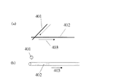
本実施例では、テラヘルツ波を伝送路303に入力させる電磁波入力手段301としては、具体的には、クロスワイヤによる入力手段を用いる。図4はクロスワイヤの具体例を示す。図4(a)は斜視図であり、図4(b)は第1ワイヤ401が伸びる方向に沿って見た図である。第1ワイヤ401と第2ワイヤ402を互いに垂直に配置することによって、電磁波403を第1ワイヤ401から第2ワイヤ402に伝搬させることが出来る。
In this embodiment, as the electromagnetic wave input means 301 for inputting the terahertz wave to the
また、伝送路303を伝播する電磁波302と検体304が相互作用する折れ曲がり部305の領域を変更し走査して検体304のイメージングなどを行う伝送路走査手段307としては、具体的には、伝送路303を可動式ステージに固定する方法がある。走査手段としては、伝送路303の方を走査する手段に限るものではなく、検体304の方を走査する手段にしてもよい。
Further, as the transmission
また、同じ伝送路を検体表面近傍に多数配置して、検体304と相互作用した電磁波302を検出する電磁波検出手段を次々と変更して行って検体304の測定部分を走査する走査手段を採用してもよい。この際、各測定部分における検体304と電磁波302の相互作用同士の影響を少なくする様に、多数配置された伝送路の折れ曲がり部間の間隔を電磁波の波長以上にしておくのが望ましい。ラスタースキャン(図3の検体304表面上の矢印参照)などの方法を用いて伝送路303を走査することで、検体304の表面全体の分析を行うこともできる。
Also, a scanning unit that scans the measurement portion of the
電磁波検出手段306としては、単一線路の端面にGaAsなどの化合物半導体を付けてフェムト秒レーザーを用いた光伝導素子がある。これにより、検体304と相互作用した電磁波によって光伝導素子で起こる電流変調を検出できる。電磁波検出手段としては、この方法に限るものではない。伝送路を伝搬する電磁波を伝送路303から一度クロスワイヤを経由させてから、クロスワイヤの端部に付属させた光伝導素子で検出するという方法を採ってもよい。後者の方法では、伝送路303とクロスするクロスワイヤの端部を移動させる必要がないので、フェムト秒レーザーなどを用いた光伝導素子による検出には向いている。
As the electromagnetic wave detection means 306, there is a photoconductive element using a femtosecond laser with a compound semiconductor such as GaAs attached to the end face of a single line. Thereby, current modulation occurring in the photoconductive element due to electromagnetic waves interacting with the
上記の様にして得られた信号波形(例えば、電流波形)のピーク値の強度を適度な階調に変換する回路系を経て、その階調変化から検体のイメージングを行うことが出来る。こうして、伝送路303を伝搬する電磁波302と検体304との相互作用領域を伝送路走査手段307によって走査して、検体表面全体の分析を行うことが出来る。検体304としては、テラヘルツ帯域に感度を持つ生体分子などがよい。この様に走査手段及びイメージングを行う回路系を設けて、折れ曲がり部で伝搬電磁波と相互作用した検体の各走査領域の表面の情報(形状や表面分析)を検出電磁波の情報から回路系で抽出して検体のイメージングを行なうことができる。
Through the circuit system that converts the intensity of the peak value of the signal waveform (for example, current waveform) obtained as described above into an appropriate gradation, the specimen can be imaged from the gradation change. In this way, the entire region of the specimen surface can be analyzed by scanning the interaction area between the
(実施例2)
図5は本発明による実施例2を示す。本実施例のセンシング装置は、電磁波入力手段と電磁波検出手段と伝送路と伝送路折れ曲がり部と伝送路被膜構造を有する。図5では、伝送路501と伝送路被膜構造502と折れ曲がり部503と電磁波504と検体505が図示されている。伝送路501を被膜する伝送路被膜構造502は、折れ曲がり部503以外の伝送路を伝搬する電磁波504と大気との相互作用効果を減らし、大気中の水分の影響による電磁波の変動を減らし、SN比を上げる為のものである。伝送路被膜構造502としては、分散性の少ない誘電体などがよく、これで伝送路501を覆うのがよい。
(Example 2)
FIG. 5 shows a second embodiment according to the present invention. The sensing device of the present embodiment has an electromagnetic wave input means, an electromagnetic wave detection means, a transmission path, a transmission path bending portion, and a transmission path coating structure. In FIG. 5, a
本実施例では、伝送路501は単一線路を使用し、電磁波入力手段と電磁波検出手段には、図3に示す様なクロスワイヤ構造を用いる。伝送路被膜構造502の作製方法は、単一線路となる金属ワイヤ構造の周囲に誘電体部材の電磁波被膜構造を取り付ける。例えば、円柱状の鋳型の中央に金属ワイヤを取り付け、伝送路被膜構造となる樹脂を流し込んで、誘電体部材を焼成して固める方法などを用いればよい。伝送路被膜構造502が被膜された金属ワイヤ501を伝送路被膜構造ごと折り曲げて、伝送路折れ曲がり部503を形成することができる。また、例えば、伝送路被膜構造502を削って当該切削部を変形させてもよいし、伝送路被膜構造502を削って折れ曲がり部503において伝送路501を伝送路被膜構造502から露出させてもよい。こうすれば、検体505と伝搬電磁波504をより近づけることが出来る。その他の点は上記実施例と同様である。
In this embodiment, the
(実施例3)
図6は本発明による実施例3を示す。本実施例のセンシング装置は、電磁波入力手段と電磁波検出手段と伝送路と折れ曲がり部と伝送路被膜構造とスペーサーを有する。図6は、伝送路601、伝送路被膜構造602、伝送路折れ曲がり部603、電磁波604、検体605、スペーサー606を図示している。
(Example 3)
FIG. 6 shows a third embodiment according to the present invention. The sensing device of this embodiment has an electromagnetic wave input means, an electromagnetic wave detection means, a transmission path, a bent portion, a transmission path coating structure, and a spacer. FIG. 6 illustrates a
スペーサー606は、伝送路601から離れるに従って電磁波の強度が変化するので、折れ曲がり部603の伝送路601と検体605の被測定領域(表面)との距離を一定に保つ為に付ける機構である。ここでは、スペーサー606は、伝送路601を被膜する伝送路被膜構造602を加工することで行っている。図6に示す様に、折れ曲がり部603の先端部に突起を形成することでスペーサー606が構成される。
The
スペーサー606の作製は、例えば、金属ワイヤをウエハに貼り付けたものや伝送路を蒸着してパターニングしたウエハに、誘電体をスピンコートによって塗布した後、フォトリソグラフィ工程とエッチング工程とレジスト除去工程などによって行う。スペーサー606の先端は突起構造がよく、この構造を採ることによって、検体表面と伝送路被膜構造602との接触面積を減らして位置分解能を上げ、検体表面の凹凸形状(図6の右側の拡大図を参照)を正しく捕らえることが可能となり、精度良く分析することが出来る。伝送路折れ曲がり部603の伝送路601と検体表面との距離(h)は、上述した様に、近傍界による相互作用効果が顕わになる伝搬電磁波604の波長オーダー以下が望ましい。その他の点は上記実施例と同様である。
The
(実施例4)
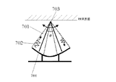
図7は本発明による実施例4を示す。本実施例のセンシング装置は、電磁波入力手段と、伝送路と、伝送路において検体と電磁波との相互作用効果を上げるための伝送路折れ曲がり部と、伝送路折れ曲がり部の折れ曲がり角度を時間的に変調する機構と、電磁波検出手段を有する。図7は、伝送路701と、電磁波702と、折れ曲がり部703と、折れ曲がり部703の折れ曲がり角度を調整する角度変調手段である駆動装置704を図示している。
(Example 4)
FIG. 7 shows a fourth embodiment according to the present invention. The sensing device of the present embodiment includes an electromagnetic wave input means, a transmission line, a transmission line bending part for increasing the interaction effect between the specimen and the electromagnetic wave in the transmission line, and a bending angle of the transmission line bending part in time. And a mechanism for detecting electromagnetic waves. FIG. 7 illustrates a
本実施例では、駆動装置704を用いて折れ曲がり部703の角度θを周期的に変化させ、折れ曲がり部703での電界分布を時間的に変調させる。これにより、ロックインアンプなどを用いて復調させることで高感度な同期検波が実現出来る。また、折り曲げ角度を変調することで、伝送路近傍の電界分布を変化させ、電磁波及び近接場からなる電磁界モードと検体との相互作用長を変えることも出来る。また、折り曲げ角度を変調して、検体と前記電磁界モードとの相互作用の有無を周波数帯域によって変化させることにより、波長選択性を持たせることも可能である。
In the present embodiment, the angle θ of the
伝送路折れ曲がりを制御する機構は、伝送路701の端部を、レールに沿って移動出来る駆動装置704に固定して、その駆動装置704をレール上で移動させる構成を採ればよい。その際、レールは図7に示す如き円弧状の構成をとることによって、伝送路折れ曲がり部703と検体表面との間隔を一定に保つことが出来る。また、その駆動装置704に折り曲げ角度を認識出来るセンサなどを取り付けておけば、なお制御性が良くなる。この折り曲げ角度は、駆動装置704がレールのどの位置にあるかを示す位置情報から、演算出来る。本実施例の角度変調手段である駆動装置704は、上記実施例のいずれの構成にも適用することができる。その他の点は上記実施例と同様である。
The mechanism for controlling the bending of the transmission path may be configured such that the end of the
101、301:電磁波入力手段(クロスワイヤ)
102、302、403、504、604、702:電磁波
103、201、303、501、601、701:伝送路
104、203、304、505、605:検体(検体表面)
105、305、503、603、703:伝送路折れ曲がり部
106、306:電磁波検出手段(クロスワイヤ)
202:伝送路を伝搬する電磁波と近接場
307:走査手段(可動ステージ)
502、602:被膜(伝送路被膜構造)
606:スペーサー
704:角度変調手段(伝送路折れ曲がり制御機構、駆動装置)
101, 301: Electromagnetic wave input means (cross wire)
102, 302, 403, 504, 604, 702: Electromagnetic waves
103, 201, 303, 501, 601, 701: Transmission path
104, 203, 304, 505, 605: Sample (sample surface)
105, 305, 503, 603, 703: Transmission line bend
106, 306: Electromagnetic wave detection means (cross wire)
202: Electromagnetic wave propagating in the transmission path and near field
307: Scanning means (movable stage)
502, 602: Coating (transmission path coating structure)
606: Spacer
704: Angle modulation means (transmission path bending control mechanism, drive unit)
Claims (6)
前記伝送路に前記テラヘルツ波を入力するための電磁波入力手段と、
前記伝送路を伝搬した前記テラヘルツ波を検出するための電磁波検出手段と、を備え、
前記伝送路は、検体との距離が前記テラヘルツ波の波長オーダー以下となるように配置される折れ曲がり部を有し、
前記電磁波検出手段は、前記検体と前記テラヘルツ波との相互作用による該テラヘルツ波の伝搬特性の変化を検出するように構成され、
前記折れ曲がり部の折れ曲がり角度を調整することで、該折れ曲がり部での電界分布を時間的に変調するための角度変調手段を更に備えることを特徴とするセンシング装置。 A transmission line having a line made of metal and propagating a terahertz wave;
An electromagnetic wave inputting means for inputting the terahertz wave to the transmission path,
Electromagnetic wave detecting means for detecting the terahertz wave propagated through the transmission path ,
The transmission line has a bent portion that is disposed so that the distance between the specimen is equal to or less than the wavelength order of the terahertz wave,
The electromagnetic wave detection unit is configured to detect a change in the propagation characteristic of the terahertz wave due to interaction between the analyte and the front Kite Raherutsu wave,
Wherein by adjusting the bending angle of the bent portion, the sensing apparatus characterized further comprising a Rukoto an angle modulation means for temporally modulating the electric field distribution at the bent portion.
検体と前記伝搬するテラヘルツ波との相互作用の領域を走査するように構成されることを特徴とする請求項1から4のいずれかに記載のセンシング装置。 Scanning means for scanning the bent portion;
Sensing device according to claim 1, characterized in that it is configured to scan a region of interaction between the terahertz wave which the propagation and specimen 4.
Priority Applications (2)
| Application Number | Priority Date | Filing Date | Title |
|---|---|---|---|
| JP2006073612A JP4732201B2 (en) | 2006-03-17 | 2006-03-17 | Sensing device using electromagnetic waves |
| US11/717,714 US7498577B2 (en) | 2006-03-17 | 2007-03-14 | Sensing device employing electromagnetic waves |
Applications Claiming Priority (1)
| Application Number | Priority Date | Filing Date | Title |
|---|---|---|---|
| JP2006073612A JP4732201B2 (en) | 2006-03-17 | 2006-03-17 | Sensing device using electromagnetic waves |
Publications (3)
| Publication Number | Publication Date |
|---|---|
| JP2007248315A JP2007248315A (en) | 2007-09-27 |
| JP2007248315A5 JP2007248315A5 (en) | 2009-04-23 |
| JP4732201B2 true JP4732201B2 (en) | 2011-07-27 |
Family
ID=38516821
Family Applications (1)
| Application Number | Title | Priority Date | Filing Date |
|---|---|---|---|
| JP2006073612A Expired - Fee Related JP4732201B2 (en) | 2006-03-17 | 2006-03-17 | Sensing device using electromagnetic waves |
Country Status (2)
| Country | Link |
|---|---|
| US (1) | US7498577B2 (en) |
| JP (1) | JP4732201B2 (en) |
Families Citing this family (18)
| Publication number | Priority date | Publication date | Assignee | Title |
|---|---|---|---|---|
| JP4217646B2 (en) * | 2004-03-26 | 2009-02-04 | キヤノン株式会社 | Authentication method and authentication apparatus |
| JP5006642B2 (en) * | 2006-05-31 | 2012-08-22 | キヤノン株式会社 | Terahertz wave oscillator |
| JP5028068B2 (en) * | 2006-05-31 | 2012-09-19 | キヤノン株式会社 | Active antenna oscillator |
| JP4861220B2 (en) * | 2006-08-28 | 2012-01-25 | キヤノン株式会社 | Inspection equipment using electromagnetic waves |
| JP4963640B2 (en) * | 2006-10-10 | 2012-06-27 | キヤノン株式会社 | Object information acquisition apparatus and method |
| JP5031330B2 (en) * | 2006-11-15 | 2012-09-19 | キヤノン株式会社 | Sample analyzer and sample analysis method |
| JP2008185552A (en) * | 2007-01-31 | 2008-08-14 | Tohoku Univ | Measuring instrument and measuring method |
| JP5043488B2 (en) | 2007-03-30 | 2012-10-10 | キヤノン株式会社 | Detection apparatus and imaging apparatus |
| EP2031374B1 (en) * | 2007-08-31 | 2012-10-10 | Canon Kabushiki Kaisha | Apparatus and method for obtaining information related to terahertz waves |
| US20090224962A1 (en) * | 2007-09-28 | 2009-09-10 | Hsueh-Yuan Pao | Apparatus And Method For Sensors Having Improved Angular Resolution |
| CN101806748B (en) * | 2010-03-25 | 2011-11-23 | 哈尔滨工业大学 | Tera-hertz two-dimensional area array scanning imaging method and imaging system for implementing same |
| JP5735824B2 (en) * | 2011-03-04 | 2015-06-17 | キヤノン株式会社 | Information acquisition apparatus and information acquisition method |
| CN102129324B (en) * | 2011-03-17 | 2012-05-02 | 汉王科技股份有限公司 | Touch control device, control method thereof and electronic equipment with touch control device |
| JP2013181929A (en) | 2012-03-04 | 2013-09-12 | Canon Inc | Measuring apparatus and method, tomography device and method |
| US9606054B2 (en) | 2013-09-30 | 2017-03-28 | Advantest Corporation | Methods, sampling device and apparatus for terahertz imaging and spectroscopy of coated beads, particles and/or microparticles |
| US9417181B2 (en) | 2014-05-08 | 2016-08-16 | Advantest Corporation | Dynamic measurement of density using terahertz radiation with real-time thickness measurement for process control |
| JP6387314B2 (en) * | 2015-03-19 | 2018-09-05 | 株式会社Nttドコモ | Wireless antenna, wireless communication system |
| KR102092463B1 (en) | 2018-07-27 | 2020-03-24 | 한양대학교 산학협력단 | Specimen Inspection Device and Specimen Inspection Method |
Citations (5)
| Publication number | Priority date | Publication date | Assignee | Title |
|---|---|---|---|---|
| JPS5811840A (en) * | 1981-07-15 | 1983-01-22 | Hitachi Ltd | Microwave alcohol fuel sensor |
| JP2000089042A (en) * | 1998-09-16 | 2000-03-31 | Furukawa Electric Co Ltd:The | Optical fiber sensor and detection of information using the same |
| JP2001517804A (en) * | 1997-09-22 | 2001-10-09 | ザ・リージェンツ・オブ・ザ・ユニバーシティ・オブ・カリフォルニア | Scanning evanescent electromagnetic microscope |
| JP2003509696A (en) * | 1999-09-10 | 2003-03-11 | ユニヴァーシティー オブ メリーランド, カレッジ パーク | Quantitative imaging of dielectric permittivity and tunability |
| JP2006066864A (en) * | 2004-07-30 | 2006-03-09 | Canon Inc | Optical semiconductor device and its manufacturing method |
Family Cites Families (9)
| Publication number | Priority date | Publication date | Assignee | Title |
|---|---|---|---|---|
| US5623145A (en) * | 1995-02-15 | 1997-04-22 | Lucent Technologies Inc. | Method and apparatus for terahertz imaging |
| US5710430A (en) * | 1995-02-15 | 1998-01-20 | Lucent Technologies Inc. | Method and apparatus for terahertz imaging |
| US6448553B1 (en) * | 1999-04-26 | 2002-09-10 | Canon Kabushiki Kaisha | Signal detector to be used with scanning probe and atomic force microscope |
| JP2002310882A (en) * | 2001-04-17 | 2002-10-23 | Canon Inc | Signal detecting device by scanning probe, probe microscope by the device, signal detecting method by scanning probe and observing method for observing sample surface using the method |
| US7062125B2 (en) * | 2003-04-08 | 2006-06-13 | Institut National D'optique | Prismatic reflection optical waveguide device |
| JP4136858B2 (en) * | 2003-09-12 | 2008-08-20 | キヤノン株式会社 | Position detection device and information input device |
| JP2006121643A (en) * | 2004-09-21 | 2006-05-11 | Canon Inc | Planar antenna |
| US7359585B2 (en) * | 2005-07-20 | 2008-04-15 | Searete Llc | Plasmon photocatalysis |
| JP4898472B2 (en) * | 2006-04-11 | 2012-03-14 | キヤノン株式会社 | Inspection device |
-
2006
- 2006-03-17 JP JP2006073612A patent/JP4732201B2/en not_active Expired - Fee Related
-
2007
- 2007-03-14 US US11/717,714 patent/US7498577B2/en not_active Expired - Fee Related
Patent Citations (5)
| Publication number | Priority date | Publication date | Assignee | Title |
|---|---|---|---|---|
| JPS5811840A (en) * | 1981-07-15 | 1983-01-22 | Hitachi Ltd | Microwave alcohol fuel sensor |
| JP2001517804A (en) * | 1997-09-22 | 2001-10-09 | ザ・リージェンツ・オブ・ザ・ユニバーシティ・オブ・カリフォルニア | Scanning evanescent electromagnetic microscope |
| JP2000089042A (en) * | 1998-09-16 | 2000-03-31 | Furukawa Electric Co Ltd:The | Optical fiber sensor and detection of information using the same |
| JP2003509696A (en) * | 1999-09-10 | 2003-03-11 | ユニヴァーシティー オブ メリーランド, カレッジ パーク | Quantitative imaging of dielectric permittivity and tunability |
| JP2006066864A (en) * | 2004-07-30 | 2006-03-09 | Canon Inc | Optical semiconductor device and its manufacturing method |
Also Published As
| Publication number | Publication date |
|---|---|
| JP2007248315A (en) | 2007-09-27 |
| US7498577B2 (en) | 2009-03-03 |
| US20070215810A1 (en) | 2007-09-20 |
Similar Documents
| Publication | Publication Date | Title |
|---|---|---|
| JP4732201B2 (en) | Sensing device using electromagnetic waves | |
| US7633299B2 (en) | Inspection apparatus using terahertz wave | |
| JP5172057B2 (en) | Device for local measurement of the complex dielectric constant of materials | |
| JP4646838B2 (en) | Probe and near-field microscope | |
| US7564034B2 (en) | Terahertz sensing apparatus using a transmission line | |
| US9178282B2 (en) | Method for coupling terahertz pulses into a coaxial waveguide | |
| US7130755B2 (en) | Near-field scanning microwave microscope using dielectric resonator | |
| JP4955966B2 (en) | Waveguide, device using the same, and detection method | |
| JP2005017644A (en) | High frequency electric signal controller and sensing system | |
| US7682567B2 (en) | Sensor for analyzing or identifying property of object, sensing apparatus using same, and sensing method | |
| Liu et al. | Integrated optical chemical sensor based on an SOI ring resonator using phase-interrogation | |
| JP2006153852A (en) | Sensor for analyzing or identifying property of object, sensing apparatus and method using the same | |
| JP4636917B2 (en) | Sample holding device, sample detection apparatus and sample detection method using the same | |
| US6573737B1 (en) | Method and apparatus for non-contact measurement of electrical properties of materials | |
| JP2007074043A (en) | Electromagnetic wave waveguide | |
| JP3462769B2 (en) | Broadband waveguide optical electric field sensor | |
| KR100517294B1 (en) | Near field microscope using waveguides resonator | |
| JP2004333167A (en) | Near field measurement method and apparatus by micro-sensor | |
| JP3853248B2 (en) | Electrical characteristic evaluation apparatus and method |
Legal Events
| Date | Code | Title | Description |
|---|---|---|---|
| A521 | Written amendment |
Free format text: JAPANESE INTERMEDIATE CODE: A523 Effective date: 20090116 |
|
| A621 | Written request for application examination |
Free format text: JAPANESE INTERMEDIATE CODE: A621 Effective date: 20090116 |
|
| A521 | Written amendment |
Free format text: JAPANESE INTERMEDIATE CODE: A523 Effective date: 20090306 |
|
| A977 | Report on retrieval |
Free format text: JAPANESE INTERMEDIATE CODE: A971007 Effective date: 20110120 |
|
| A131 | Notification of reasons for refusal |
Free format text: JAPANESE INTERMEDIATE CODE: A131 Effective date: 20110125 |
|
| A521 | Written amendment |
Free format text: JAPANESE INTERMEDIATE CODE: A523 Effective date: 20110322 |
|
| TRDD | Decision of grant or rejection written | ||
| A01 | Written decision to grant a patent or to grant a registration (utility model) |
Free format text: JAPANESE INTERMEDIATE CODE: A01 Effective date: 20110411 |
|
| A01 | Written decision to grant a patent or to grant a registration (utility model) |
Free format text: JAPANESE INTERMEDIATE CODE: A01 |
|
| A61 | First payment of annual fees (during grant procedure) |
Free format text: JAPANESE INTERMEDIATE CODE: A61 Effective date: 20110420 |
|
| FPAY | Renewal fee payment (event date is renewal date of database) |
Free format text: PAYMENT UNTIL: 20140428 Year of fee payment: 3 |
|
| R150 | Certificate of patent or registration of utility model |
Free format text: JAPANESE INTERMEDIATE CODE: R150 |
|
| LAPS | Cancellation because of no payment of annual fees |