JP4732183B2 - Image processing apparatus, image processing method, and program for causing computer to execute the method - Google Patents
Image processing apparatus, image processing method, and program for causing computer to execute the method Download PDFInfo
- Publication number
- JP4732183B2 JP4732183B2 JP2006044145A JP2006044145A JP4732183B2 JP 4732183 B2 JP4732183 B2 JP 4732183B2 JP 2006044145 A JP2006044145 A JP 2006044145A JP 2006044145 A JP2006044145 A JP 2006044145A JP 4732183 B2 JP4732183 B2 JP 4732183B2
- Authority
- JP
- Japan
- Prior art keywords
- memory
- image
- address
- mask
- access
- Prior art date
- Legal status (The legal status is an assumption and is not a legal conclusion. Google has not performed a legal analysis and makes no representation as to the accuracy of the status listed.)
- Expired - Fee Related
Links
- 238000012545 processing Methods 0.000 title claims description 280
- 238000000034 method Methods 0.000 title claims description 62
- 238000003672 processing method Methods 0.000 title claims description 31
- 238000004364 calculation method Methods 0.000 claims description 60
- 238000012546 transfer Methods 0.000 claims description 47
- 238000004519 manufacturing process Methods 0.000 claims description 2
- 238000010586 diagram Methods 0.000 description 17
- 238000003860 storage Methods 0.000 description 11
- 230000000873 masking effect Effects 0.000 description 9
- 238000012986 modification Methods 0.000 description 6
- 230000004048 modification Effects 0.000 description 6
- 238000006243 chemical reaction Methods 0.000 description 4
- 230000000694 effects Effects 0.000 description 3
- 239000004973 liquid crystal related substance Substances 0.000 description 3
- 230000002093 peripheral effect Effects 0.000 description 3
- 238000005516 engineering process Methods 0.000 description 2
- 230000010365 information processing Effects 0.000 description 2
- 238000012805 post-processing Methods 0.000 description 2
- 230000005540 biological transmission Effects 0.000 description 1
- 238000012937 correction Methods 0.000 description 1
- 238000013500 data storage Methods 0.000 description 1
- 238000011161 development Methods 0.000 description 1
- 238000009792 diffusion process Methods 0.000 description 1
- 238000009826 distribution Methods 0.000 description 1
- 230000006870 function Effects 0.000 description 1
- 239000011159 matrix material Substances 0.000 description 1
- 238000004080 punching Methods 0.000 description 1
- 230000003068 static effect Effects 0.000 description 1
- 239000002699 waste material Substances 0.000 description 1
Images


Description
本発明は、画像処理装置、画像処理方法、その方法をコンピュータに実行させるプログラムに関するものである。 The present invention relates to an image processing apparatus, an image processing method, and a program for causing a computer to execute the method.
従来、画像形成装置において、画像を回転するためには、画像をある矩形に区切り、ブロック単位でメモリから読み込み、回転した後、ブロック単位でメモリに書き戻すことを繰り返していた。例えば、1bit2値の画像を回転する際に、一つのブロックを256×256画素とすると、主走査方向に64バイト、副走査方向に256ラインのブロックを、メモリから回転器のSRAM(Static RAM)に読み込みながら回転し、メモリの書き込み位置に書き込んでいた。 Conventionally, in an image forming apparatus, in order to rotate an image, the image is divided into certain rectangles, read from the memory in units of blocks, rotated, and then written back to the memory in units of blocks. For example, when rotating a 1-bit binary image, if one block is 256 × 256 pixels, a block of 64 bytes in the main scanning direction and 256 lines in the sub-scanning direction is transferred from the memory to the rotator SRAM (Static RAM). Rotate while reading and writing to the memory write position.
ここで、ブロック単位でメモリにアクセスする場合、一般に、ブロックのスタートアドレスが、メモリバス幅というHW制約によって制限を受ける。もしこれを無視して、例えば32bit幅のメモリに対してバイト単位でスタートアドレスを設定すると、メモリアクセスのアドレス発生方法が複雑になる他、実装に従ってHWを設計しないとメモリアクセスの増加によるパフォーマンスの低下がおこる。 Here, when accessing the memory in units of blocks, the start address of the block is generally limited by the HW restriction of the memory bus width. If this is ignored and the start address is set in units of bytes for a 32-bit width memory, for example, the memory access address generation method becomes complicated, and if the HW is not designed according to the implementation, the performance of the memory access increases. Decrease occurs.
例えば、画像を90度または270度回転させる場合、回転後画像の画像配置(メモリ上のアドレス)まで考慮して画像をブロック化しないと、パフォーマンスが低下する。一般に、回転前画像も回転後画像も、特定のバウンダリ制約を満たしたメモリ上のアドレス、主走査長、副走査長の画像しか回転できなかった。従って、回転するためのブロックは固定であり、半端なサイズの画像や、半端なメモリ位置(アドレス)に置かれた画像を回転することは出来なかった。 For example, when an image is rotated 90 degrees or 270 degrees, performance is degraded unless the image is blocked in consideration of the image layout (address on the memory) of the rotated image. In general, both the pre-rotation image and the post-rotation image can be rotated only in the memory address, main scanning length, and sub-scanning length that satisfy specific boundary constraints. Therefore, the block for rotation is fixed, and an image having an odd size or an image placed at an odd memory location (address) cannot be rotated.
このような問題を解決するために、特許文献1の技術では、画像の回転処理において、ブロック単位で回転処理を施す回転処理単位を4バイトで行い、これに合わせてメモリへのアクセス単位も4バイトに設定している。同文献の技術においては、入力先頭アドレスが回転処理単位にアラインされていない場合、即ち格子と回転処理単位の先頭部分とが一致していない場合は、入力先頭アドレスの下位数ビットを0にしてアラインさせると同時に、マスク量を計算してマスク処理を施しながら、出力手段に出力させていた。 In order to solve such a problem, in the technique of Patent Document 1, the rotation processing unit for performing the rotation processing in units of blocks is performed by 4 bytes in the image rotation processing, and the access unit to the memory is also set to 4 bytes accordingly. Set to byte. In the technique of this document, when the input head address is not aligned with the rotation processing unit, that is, when the grid and the head part of the rotation processing unit do not match, the lower-order bits of the input head address are set to 0. At the same time as aligning, the masking amount is calculated and masked, and then output to the output means.
図11は、従来例による画像の回転処理における入力アドレスの生成を説明する図である。ここで、回転処理単位1110を決定する格子1101(図中点線で表された格子)は、下位2ビットを0とするもの、即ち、入力アドレスが[1:0]=0のものである。図11に示すように、回転処理単位1110は4バイト(32×32ビット)であり、メモリへのアクセス単位も4バイトとなる。また、メモリのアドレスはバイト単位である。 FIG. 11 is a diagram for explaining generation of an input address in the image rotation processing according to the conventional example. Here, a lattice 1101 (a lattice represented by a dotted line in the figure) for determining the rotation processing unit 1110 is one in which the lower 2 bits are 0, that is, the input address is [1: 0] = 0. As shown in FIG. 11, the rotation processing unit 1110 is 4 bytes (32 × 32 bits), and the memory access unit is 4 bytes. The memory address is in bytes.
この従来例では入力先頭アドレスが回転処理単位にアラインされていない場合、例えば領域1111における図中の左上の頂点1111aの場合、入力アドレス変換手段が、入力先頭アドレスの下位数ビットを0にすると同時に、マスク量を計算し、出力手段へ出力する。図中、アラインされていない回転処理単位においては、データ1120中のデータ1121がマスクされる部分である。従って、有効データは、図中データ1122〜1124で表されるように、4バイトから1バイトを引いた3バイト分だけとなってしまう。
In this conventional example, when the input head address is not aligned in the rotation processing unit, for example, in the case of the upper
しかしながら、この方式では、回転ブロックが小さな場合は、入力先頭アドレスを変換しマスク量を計算する回数が増加して、メモリアクセスに無駄があった。また、この方式のままで回転処理単位を大きくした場合には、マスクされるビット数が多くなり、使用しないアドレスの読み込みが増加して、メモリアクセスに無駄があった。 However, in this method, when the rotating block is small, the number of times of converting the input head address and calculating the mask amount is increased, and the memory access is wasted. Further, when the rotation processing unit is increased with this method, the number of bits to be masked increases, reading of unused addresses increases, and memory access is wasted.
本発明は上記の問題に鑑みてなされ、その目的は、無駄なメモリアクセスを省略でき、画像処理効率の高い画像処理装置、画像処理方法、その方法をコンピュータに実行させるプログラムを提供することである。 The present invention has been made in view of the above problems, and an object thereof is to provide an image processing apparatus, an image processing method, and a program for causing a computer to execute the method, which can eliminate useless memory access and have high image processing efficiency. .
上述した課題を解決し、目的を達成するために、請求項1にかかる発明は、画像データを格納する画像メモリを矩形領域に分割する分割手段と、前記画像メモリから前記画像データを読み出す入力メモリアドレスを生成する入力アドレス生成手段と、前記入力アドレス生成手段によって生成された入力メモリアドレスに基づいて、前記画像メモリにバーストアクセスして、画像データを読み出すメモリアクセス制御手段と、前記入力アドレス生成手段によって生成された入力アドレスに基づいて前記画像データを読み込んで回転処理を施す回転処理手段と、を備え、前記入力アドレス生成手段は、前記画像メモリに格納された画像データを読み出す主走査方向の先頭メモリアドレスであって前記分割手段によって分割された矩形領域の先頭アドレスを生成する先頭メモリアドレス生成手段、および、主走査方向の所定幅における先頭画素からの非アクセス量である先頭非アクセス量、前記主走査方向の所定幅における後端画素に至るまでの非アクセス量である後端非アクセス量、及び前記メモリアクセス制御手段がバーストアクセスする前記矩形領域内におけるバースト長を演算することにより、前記先頭メモリアドレス生成手段によって生成された先頭アドレスに対応する画素以降の読み込みを停止する画素数を演算する非アクセス量演算手段を、有し、前記メモリアクセス制御手段は、前記先頭アドレスに対応する画素以降、前記非アクセス量演算手段によって前記先頭非アクセス量、前記後端非アクセス量、および前記バースト長に基づいて演算された画素数の画像データを読み飛ばして前記画像メモリにバーストアクセスし、格納された画像データを読み出し、前記回転処理手段によって回転処理を施された画像データを、前記画像メモリにバースト転送するものであることを特徴とする。 In order to solve the above-described problems and achieve the object, the invention according to claim 1 includes a dividing means for dividing an image memory for storing image data into rectangular areas, and an input memory for reading out the image data from the image memory. Input address generation means for generating an address; memory access control means for reading out image data by burst access to the image memory based on the input memory address generated by the input address generation means; and the input address generation means Rotation processing means for reading the image data on the basis of the input address generated by the input address and performing rotation processing, and the input address generation means reads the image data stored in the image memory in the main scanning direction. beginning a of the divided rectangular areas by said division means a memory address The first memory address generating means for generating less, and, the top non-access amount is non-accessible volume of the head pixel in a predetermined width in the main scanning direction, a non-access up to the rear end pixel in the predetermined width of the main scanning direction rear non-access amount is an amount, and the by the memory access control means for calculating a burst length in the rectangular region to burst access, a pixel corresponding to the first memory address previously Atamaa dress generated by the generating means the non-access amount calculating means for calculating the number of pixels to stop reading after having the memory access control means, after a pixel corresponding to the destination Atamaa dress, the leading non-access by the non-access amount calculation means the amount, the rear end non-access amount, and the image data of the number of pixels that have been calculated based on the burst length Skip viewed burst accesses in the image memory reads the stored image data, the image data subjected to rotation processing by the rotation processing unit, and characterized in that the burst transfer to the image memory.
請求項2にかかる発明は、請求項1に記載の画像処理装置において、前記画像メモリアクセス制御手段によって読み出された画像データを、画像メモリに格納するための出力メモリアドレスを生成する出力アドレス生成手段を、さらに備え、前記メモリアクセス制御手段は、前記出力アドレス生成手段によって生成された出力メモリアドレスに基づいて、読み出した前記画像データを、前記画像メモリにバースト転送するものであることを特徴とする。 Such invention in claim 2, the image processing apparatus according to claim 1, the image data read by the image memory access control means, generating an output address for generating an output memory address for storage in the image memory The memory access control means burst-transfers the read image data to the image memory based on the output memory address generated by the output address generation means. To do.
請求項3にかかる発明は、請求項2に記載の画像処理装置において、前記メモリアクセス制御手段は、前記出力メモリアドレス、および前記バースト長に基づいて、前記読み出した画像データを、前記画像メモリにバースト転送するものであることを特徴とする。
Such invention in
請求項4にかかる発明は、請求項2または3に記載の画像処理装置において、前記メモリアクセス制御手段は、前記画像データを前記画像メモリに格納する際に、所定数の画素データに対してマスク処理を施して格納するマスク生成手段を有するものであることを特徴とする。 According to a fourth aspect of the present invention, in the image processing apparatus according to the second or third aspect , the memory access control unit masks a predetermined number of pixel data when storing the image data in the image memory. It has a mask generation means for performing processing and storing it.
請求項5にかかる発明は、請求項4に記載の画像処理装置において、前記マスク生成手段は、上記先頭読み飛ばしに後続する所定の画素数だけマスク処理を施す先頭マスク生成手段、および、上記後端読み飛ばしに先行する所定の画素数だけマスク処理を施す後端マスク生成手段を有し、前記先頭マスク生成手段によるマスク処理、および前記後端マスク生成手段によるマスク処理によって、前記画像データに対してマスク処理を施すものであることを特徴とする。 According to a fifth aspect of the present invention, in the image processing apparatus according to the fourth aspect , the mask generation unit performs a mask process for a predetermined number of pixels subsequent to the head reading skip, and the rear A rear end mask generation unit that performs mask processing for a predetermined number of pixels preceding skipping of the end reading, and the image data is subjected to mask processing by the head mask generation unit and mask processing by the rear end mask generation unit; The mask processing is performed.
請求項6にかかる発明は、請求項1〜5のいずれか1つに記載の画像処理装置において、前記分割手段は、前記画像メモリをバイト単位の矩形領域に分割するものであることを特徴とする。 According to a sixth aspect of the present invention, in the image processing apparatus according to any one of the first to fifth aspects, the dividing unit divides the image memory into rectangular areas in units of bytes. To do.
請求項7にかかる発明は、画像処理装置における画像処理方法であって、分割手段によって、画像データを格納する画像メモリを矩形領域に分割する分割工程と、入力アドレス生成手段によって、前記画像メモリから前記画像データを読み出す入力メモリアドレスを生成する入力アドレス生成工程と、メモリアクセス制御手段によって、前記入力アドレス生成工程で生成された入力メモリアドレスに基づいて、前記画像メモリにバーストアクセスして、画像データを読み出すメモリアクセス制御工程と、回転処理手段によって、前記入力アドレス生成工程で生成された入力アドレスに基づいて前記画像データを読み込んで回転処理を施す回転処理工程と、を含み、前記入力アドレス生成工程は、先頭メモリアドレス生成手段によって、前記画像メモリに格納された画像データを読み出す主走査方向の先頭メモリアドレスであって前記分割工程で分割された矩形領域の先頭アドレスを生成する先頭メモリアドレス生成工程、および、非アクセス量演算手段によって、主走査方向の所定幅における先頭画素からの非アクセス量である先頭非アクセス量、前記主走査方向の所定幅における後端画素に至るまでの非アクセス量である後端非アクセス量、及び前記メモリアクセス制御手段がバーストアクセスする前記矩形領域内におけるバースト長を演算することにより、前記先頭メモリアドレス生成工程で生成された先頭アドレスに対応する画素以降の読み込みを停止する画素数を演算する非アクセス量演算工程を、含み、前記メモリアクセス制御工程は、前記先頭アドレスに対応する画素以降、前記非アクセス量演算工程で前記先頭非アクセス量、前記後端非アクセス量、および前記バースト長に基づいて演算された画素数の画像データを読み飛ばして前記画像メモリにバーストアクセスし、格納された画像データを読み出し、前記回転処理工程で回転処理を施された画像データを、前記画像メモリにバースト転送するものであることを特徴とする。 Such invention in claim 7, an image processing method in images processing device, the dividing means, a dividing step of dividing an image memory for storing image data in the rectangular area, the input address generating unit, the image memory An input address generation step for generating an input memory address for reading the image data from the memory, and a burst access to the image memory based on the input memory address generated in the input address generation step by the memory access control means, A memory access control step for reading data; and a rotation processing step for reading the image data and performing rotation processing based on the input address generated in the input address generation step by a rotation processing means, and generating the input address The process is performed by the top memory address generating means. The first memory address generating step of generating the start address of the divided rectangular area in the division step a first memory address in the main scanning direction for reading the image data stored in the memory, and, by non-access amount calculation means, a main A head non-access amount that is a non-access amount from the head pixel in a predetermined width in the scanning direction, a rear end non-access amount that is a non-access amount up to a rear end pixel in the predetermined width in the main scanning direction, and the memory access by controlling means for calculating a burst length within the rectangular area to be burst access, non-access for calculating the number of pixels to stop reading the subsequent pixel corresponding to the first memory address generated by the generating step the previously Atamaa dress the amount calculating step, wherein, the memory access control step, pixels corresponding to the destination Atamaa dress Descending, wherein the first non-access amount in a non-access amount calculation step, the rear end non-access volume and burst accesses in the image memory skip image data of the number of pixels is calculated based on the burst length, stores The read image data is read out, and the image data subjected to the rotation process in the rotation process step is burst-transferred to the image memory.
請求項8にかかる発明は、請求項7に記載の画像処理方法において、出力アドレス生成手段によって、前記画像メモリアクセス制御工程で読み出された画像データを、画像メモリに格納するための出力メモリアドレスを生成する出力アドレス生成工程を、さらに含み、前記メモリアクセス制御工程は、前記メモリアクセス制御手段が、前記出力アドレス生成工程で生成された出力メモリアドレスに基づいて、読み出した前記画像データを、前記画像メモリにバースト転送するものであることを特徴とする。 According to an eighth aspect of the present invention, in the image processing method according to the seventh aspect , the output memory address for storing the image data read out in the image memory access control step by the output address generating means in the image memory. An output address generation step for generating the memory access control step, wherein the memory access control means reads the image data read out based on the output memory address generated in the output address generation step; It is characterized by burst transfer to the image memory.
請求項9にかかる発明は、請求項8に記載の画像処理方法において、前記メモリアクセス制御工程は、前記メモリアクセス制御手段が、前記出力メモリアドレス、および前記バースト長に基づいて、前記読み出した画像データを前記画像メモリにバースト転送するものであることを特徴とする。 According to a ninth aspect of the present invention, in the image processing method according to the eighth aspect , in the memory access control step, the memory access control means reads the read image based on the output memory address and the burst length. The data is burst-transferred to the image memory.
請求項10にかかる発明は、請求項8または9に記載の画像処理方法において、前記メモリアクセス制御工程は、前記メモリアクセス制御手段が、前記画像データを前記画像メモリに格納する際に、マスク生成手段によって、所定数の画素データに対してマスク処理を施して格納するマスク生成工程を、含むものであることを特徴とする。 According to a tenth aspect of the present invention, in the image processing method according to the eighth or ninth aspect , the memory access control step generates a mask when the memory access control means stores the image data in the image memory. The method includes a mask generation step of performing mask processing on a predetermined number of pixel data by means and storing.
請求項11にかかる発明は、請求項10に記載の画像処理方法において、前記マスク生成工程は、先頭マスク生成手段によって、上記先頭読み飛ばしに後続する所定の画素数だけマスク処理を施す先頭マスク生成工程、および、後端マスク生成手段によって、上記後端読み飛ばしに先行する所定の画素数だけマスク処理を施す後端マスク生成工程を含み、前記先頭マスク生成手段によるマスク処理、および前記後端マスク生成手段によるマスク処理によって、前記画像データに対してマスク処理を施すものであることを特徴とする。 According to an eleventh aspect of the present invention, in the image processing method according to the tenth aspect , in the mask generation step, the mask generation step performs mask processing for a predetermined number of pixels following the head reading skip by the head mask generation means. And a rear end mask generating step of performing mask processing by a predetermined number of pixels preceding the rear end skipping by the rear end mask generating means, and mask processing by the head mask generating means and the rear end mask A mask process is performed on the image data by a mask process by a generation unit.
請求項12にかかる発明は、請求項7〜11のいずれか1つに記載の画像処理方法において、前記分割工程は、前記分割手段が、前記画像メモリをバイト単位の矩形領域に分割するものであることを特徴とする。 According to a twelfth aspect of the present invention, in the image processing method according to any one of the seventh to eleventh aspects, the dividing step divides the image memory into rectangular areas in units of bytes. It is characterized by being.
請求項13にかかる発明は、プログラムにおいて、請求項7〜12のいずれか1つに記
載の画像処理方法を、コンピュータに実行させることを特徴とする。
According to a thirteenth aspect of the present invention, a program causes a computer to execute the image processing method according to any one of the seventh to twelfth aspects.
請求項1にかかる発明によれば、画像データを格納する画像メモリから画像データを読み出す入力メモリアドレスを生成し、生成された入力メモリアドレスに基づいて、画像メモリにバーストアクセスして、画像データを読み出すので、メモリアクセスを省略でき、画像処理効率の高い画像処理装置を提供できるという効果を奏する。 According to the first aspect of the present invention, the input memory address for reading the image data from the image memory storing the image data is generated, and the image memory is burst-accessed based on the generated input memory address to Since reading is performed, memory access can be omitted, and an image processing apparatus with high image processing efficiency can be provided.
また、請求項1にかかる発明によれば、画像メモリに格納された画像データを読み出す主走査方向の先頭メモリアドレスを生成し、生成された先頭メモリアドレスに対応する画素以降の読み込みを停止する画素数を演算し、先頭メモリアドレスに対応する画素以降、演算された画素数の画像データを読み飛ばして画像メモリにバーストアクセスし、格納された画像データを読み出すことによって、不必要な画素に対応するメモリにアクセスすることが無いので、メモリアクセスを省略でき、画像処理効率の高い画像処理装置を提供できるという効果を奏する。
また、請求項1にかかる発明によれば、生成された入力アドレスに基づいて画像データを読み込んで回転処理を施す回転処理し、回転処理を施された画像データを、画像メモリにバースト転送することによって、画像の回転処理においても、メモリアクセスを省略でき、画像処理効率の高い画像処理装置を提供できるという効果を奏する。
According to the first aspect of the present invention, the top memory address in the main scanning direction for reading the image data stored in the image memory is generated, and the pixels that stop reading from the pixel corresponding to the generated top memory address are stopped. After the pixel corresponding to the head memory address is calculated, the image data corresponding to the calculated pixel number is skipped, the image memory is burst-accessed, and the stored image data is read to cope with unnecessary pixels. Since the memory is not accessed, the memory access can be omitted, and an image processing apparatus with high image processing efficiency can be provided.
According to the first aspect of the present invention, the image data is read based on the generated input address, is subjected to rotation processing, and the rotation-processed image data is burst transferred to the image memory. As a result, memory access can be omitted even in image rotation processing, and an image processing apparatus with high image processing efficiency can be provided.
請求項1にかかる発明によれば、主走査方向の所定幅における先頭画素からの非アクセス量である先頭非アクセス量を演算し、主走査方向の所定幅における後端画素に至るまでの非アクセス量である後端非アクセス量を演算し、バーストアクセスするバースト長を演算し、先頭メモリアドレス、先頭非アクセス量、後端非アクセス量、およびバースト長に基づいて、画像メモリにバーストアクセスするので、主走査方向に沿った先頭と後端における不必要な画素に対応するメモリにアクセスすることが無いので、メモリアクセスを省略でき、画像処理効率の高い画像処理装置を提供できるという効果を奏する。
また、請求項1にかかる発明によれば、画像メモリを矩形領域に分割し、分割された矩形領域の先頭アドレスを生成し、矩形領域内におけるバースト長を演算してバースト転送することによって、メモリアクセスを省略でき、画像処理効率の高い画像処理装置を提供できるという効果を奏する。
According to the first aspect of the present invention, the head non-access amount, which is the non-access amount from the head pixel in the predetermined width in the main scanning direction, is calculated, and non-access until the rear end pixel in the predetermined width in the main scanning direction is reached. Since the rear end non-access amount, which is the amount, is calculated, the burst length for burst access is calculated, and the burst access to the image memory is performed based on the head memory address, the head non-access amount, the rear end non-access amount, and the burst length. Since there is no access to the memory corresponding to unnecessary pixels at the head and rear ends along the main scanning direction, memory access can be omitted, and an image processing apparatus with high image processing efficiency can be provided.
According to the first aspect of the invention, the image memory is divided into rectangular areas, the start address of the divided rectangular area is generated, the burst length in the rectangular area is calculated, and burst transfer is performed. Access can be omitted, and an image processing apparatus with high image processing efficiency can be provided.
請求項2にかかる発明によれば、読み出された画像データを、画像メモリに格納するための出力メモリアドレスを生成して、出力メモリアドレスに基づいて、読み出した画像データを、画像メモリにバースト転送することによって、不必要な画素に対応するメモリにアクセスすることが無く転送するので、メモリアクセスを省略でき、画像処理効率の高い画像処理装置を提供できるという効果を奏する。 According to the invention of claim 2 , an output memory address for storing the read image data in the image memory is generated, and the read image data is burst to the image memory based on the output memory address. Since the transfer is performed without accessing a memory corresponding to an unnecessary pixel, the memory access can be omitted and an image processing apparatus with high image processing efficiency can be provided.
請求項3にかかる発明によれば、出力メモリアドレス、およびバースト長に基づいて、読み出した画像データを画像メモリにバースト転送することによって、出力メモリアドレスにアクセスするだけでバースト書き込みを行うので、メモリアクセスを省略でき、画像処理効率の高い画像処理装置を提供できるという効果を奏する。 According to the third aspect of the present invention, since the read image data is burst-transferred to the image memory based on the output memory address and the burst length, burst writing is performed only by accessing the output memory address. Access can be omitted, and an image processing apparatus with high image processing efficiency can be provided.
請求項4にかかる発明によれば、画像データを画像メモリに格納する際に、所定数の画素データに対してマスク処理を施して格納するので、不必要な書き込みを省略でき、効率が高く、メモリアクセスを省略でき、画像処理効率の高い画像処理装置を提供できるという効果を奏する。
According to the invention of
請求項5にかかる発明によれば、マスク処理においては、先頭非アクセス量に後続する所定の画素数だけマスク処理を施し、後端非アクセス量に先行する所定の画素数だけマスク処理を施すことによって、画像データを画像メモリに格納する際に、所定数の画素データに対して主走査方向の所定幅において先頭と後端の両方においてマスク処理を施して格納するので、不必要な書き込みを省略でき、効率が高く、メモリアクセスを省略でき、画像処理効率の高い画像処理装置を提供できるという効果を奏する。 According to the fifth aspect of the present invention, in the mask process, the mask process is performed for a predetermined number of pixels following the head non-access amount, and the mask process is performed for a predetermined number of pixels preceding the rear end non-access amount. Therefore, when storing the image data in the image memory, the predetermined number of pixel data are masked and stored at both the front and rear ends in a predetermined width in the main scanning direction, so unnecessary writing is omitted. Therefore, it is possible to provide an image processing apparatus with high efficiency, high memory efficiency, and high image processing efficiency.
請求項6にかかる発明によれば、分割においては、画像メモリをバイト単位の矩形領域に分割することによって、バイト単位でバーストアクセスすることができるので、メモリアクセスを省略でき、画像処理効率の高い画像処理装置を提供できるという効果を奏する。
According to the invention of
請求項7にかかる発明によれば、画像データを格納する画像メモリから画像データを読み出す入力メモリアドレスを生成し、生成された入力メモリアドレスに基づいて、画像メモリにバーストアクセスして、画像データを読み出すので、メモリアクセスを省略でき、画像処理効率の高い画像処理方法を提供できるという効果を奏する。 According to the invention of claim 7 , the input memory address for reading the image data from the image memory storing the image data is generated, and the image memory is burst-accessed based on the generated input memory address, and the image data is Since reading is performed, memory access can be omitted, and an image processing method with high image processing efficiency can be provided.
また、請求項7にかかる発明によれば、画像メモリに格納された画像データを読み出す主走査方向の先頭メモリアドレスを生成し、生成された先頭メモリアドレスに対応する画素以降の読み込みを停止する画素数を演算し、先頭メモリアドレスに対応する画素以降、演算された画素数の画像データを読み飛ばして画像メモリにバーストアクセスし、格納された画像データを読み出すことによって、不必要な画素に対応するメモリにアクセスすることが無いので、メモリアクセスを省略でき、画像処理効率の高い画像処理方法を提供できるという効果を奏する。
また、請求項7にかかる発明によれば、生成された入力アドレスに基づいて画像データを読み込んで回転処理を施す回転処理し、回転処理を施された画像データを、画像メモリにバースト転送することによって、画像の回転処理においても、メモリアクセスを省略でき、画像処理効率の高い画像処理方法を提供できるという効果を奏する。
According to the seventh aspect of the present invention, a top memory address in the main scanning direction for reading image data stored in the image memory is generated, and a pixel that stops reading after the pixel corresponding to the generated top memory address After the pixel corresponding to the head memory address is calculated, the image data corresponding to the calculated pixel number is skipped, the image memory is burst-accessed, and the stored image data is read to cope with unnecessary pixels. Since the memory is not accessed, the memory access can be omitted, and an image processing method with high image processing efficiency can be provided.
According to the seventh aspect of the present invention, the image data is read based on the generated input address, the rotation process is performed to perform the rotation process, and the image data subjected to the rotation process is burst transferred to the image memory. As a result, memory access can be omitted even in image rotation processing, and an image processing method with high image processing efficiency can be provided.
請求項7にかかる発明によれば、主走査方向の所定幅における先頭画素からの非アクセス量である先頭非アクセス量を演算し、主走査方向の所定幅における後端画素に至るまでの非アクセス量である後端非アクセス量を演算し、バーストアクセスするバースト長を演算し、先頭メモリアドレス、先頭非アクセス量、後端非アクセス量、およびバースト長に基づいて、画像メモリにバーストアクセスするので、主走査方向に沿った先頭と後端における不必要な画素に対応するメモリにアクセスすることが無いので、メモリアクセスを省略でき、画像処理効率の高い画像処理方法を提供できるという効果を奏する。
また、請求項7にかかる発明によれば、画像メモリを矩形領域に分割し、分割された矩形領域の先頭アドレスを生成し、矩形領域内におけるバースト長を演算してバースト転送することによって、メモリアクセスを省略でき、画像処理効率の高い画像処理方法を提供できるという効果を奏する。
According to the seventh aspect of the present invention, the head non-access amount that is the non-access amount from the head pixel in the predetermined width in the main scanning direction is calculated, and the non-access until the rear end pixel in the predetermined width in the main scanning direction is reached. Since the rear end non-access amount that is the amount is calculated, the burst length for burst access is calculated, and burst access is performed to the image memory based on the top memory address, the top non-access amount, the rear end non-access amount, and the burst length. Since there is no access to the memory corresponding to unnecessary pixels at the head and rear ends along the main scanning direction, memory access can be omitted, and an image processing method with high image processing efficiency can be provided.
According to the invention of claim 7 , the image memory is divided into rectangular areas, the start address of the divided rectangular area is generated, the burst length in the rectangular area is calculated, and burst transfer is performed. Access can be omitted, and an image processing method with high image processing efficiency can be provided.
請求項8にかかる発明によれば、読み出された画像データを、画像メモリに格納するための出力メモリアドレスを生成して、出力メモリアドレスに基づいて、読み出した画像データを、画像メモリにバースト転送することによって、不必要な画素に対応するメモリにアクセスすることが無く転送するので、メモリアクセスを省略でき、画像処理効率の高い画像処理方法を提供できるという効果を奏する。 According to the eighth aspect of the present invention, an output memory address for storing the read image data in the image memory is generated, and the read image data is burst to the image memory based on the output memory address. Since the transfer is performed without accessing a memory corresponding to an unnecessary pixel, the memory access can be omitted and an image processing method with high image processing efficiency can be provided.
請求項9にかかる発明によれば、出力メモリアドレス、およびバースト長に基づいて、読み出した画像データを画像メモリにバースト転送することによって、出力メモリアドレスにアクセスするだけでバースト書き込みを行うので、メモリアクセスを省略でき、画像処理効率の高い画像処理方法を提供できるという効果を奏する。 According to the ninth aspect of the present invention, since the read image data is burst-transferred to the image memory on the basis of the output memory address and the burst length, burst writing is performed only by accessing the output memory address. Access can be omitted, and an image processing method with high image processing efficiency can be provided.
請求項10にかかる発明によれば、画像データを画像メモリに格納する際に、所定数の画素データに対してマスク処理を施して格納するので、不必要な書き込みを省略でき、効率が高く、メモリアクセスを省略でき、画像処理効率の高い画像処理方法を提供できるという効果を奏する。
According to the invention of
請求項11にかかる発明によれば、マスク処理においては、先頭非アクセス量に後続する所定の画素数だけマスク処理を施し、後端非アクセス量に先行する所定の画素数だけマスク処理を施すことによって、画像データを画像メモリに格納する際に、所定数の画素データに対して主走査方向の所定幅において先頭と後端の両方においてマスク処理を施して格納するので、不必要な書き込みを省略でき、効率が高く、メモリアクセスを省略でき、画像処理効率の高い画像処理方法を提供できるという効果を奏する。
According to the invention of
請求項12にかかる発明によれば、分割においては、画像メモリをバイト単位の矩形領域に分割することによって、バイト単位でバーストアクセスすることができるので、メモリアクセスを省略でき、画像処理効率の高い画像処理方法を提供できるという効果を奏する。 According to the twelfth aspect of the present invention, in the division, the image memory is divided into rectangular areas in units of bytes, whereby burst access can be performed in units of bytes, so that memory access can be omitted, and image processing efficiency is high. There is an effect that an image processing method can be provided.
請求項13にかかる発明によれば、請求項7〜12のいずれか1つに記載の画像処理方法を、コンピュータに実行させるプログラムを提供できるという効果を奏する。 According to the invention concerning Claim 13, there exists an effect that the program which makes a computer perform the image processing method as described in any one of Claims 7-12 can be provided.
以下に添付図面を参照して、この発明にかかる画像処理装置、画像処理方法、その方法をコンピュータに実行させるプログラムの最良な実施の形態、および変形例を詳細に説明する。 DETAILED DESCRIPTION Exemplary embodiments of an image processing apparatus, an image processing method, and a program for causing a computer to execute the method according to the present invention will be described below in detail with reference to the accompanying drawings.
(実施の形態)
実施の形態による画像処理装置は、画像情報を読み込み回転処理単位に分割して回転処理を施す際に、回転処理単位の先頭アドレスとバースト長情報を取得し、読み込みの先頭アドレスからバーストアクセスして読み込む。回転後に書き込む際には、書き込みの先頭アドレスからバースト転送して書き込む。
(Embodiment)
When the image processing apparatus according to the embodiment divides the image information into read rotation processing units and performs rotation processing, the image processing apparatus acquires the start address and burst length information of the rotation processing unit, and performs burst access from the read start address. Read. When writing after rotation, burst transfer is performed from the start address of writing.
そして、回転処理単位における画素データの先頭アドレスが回転処理単位にアラインされていない場合は、メモリアクセスしない部分を読み飛ばし、かつ画像データのない部分にマスク処理を施して、バースト転送して書き込む。即ち、先頭アドレスを決定し、メモリアクセスしない部分を設定して読み込み、必要なビット数だけのマスクを設定して、バースト転送することによって、回転前画像と回転後画像のスタートアドレスをバイト単位で設定でき、アラインしない領域においては不必要なメモリアクセスを停止し、かつマスク処理を施してバースト転送することによって無駄なメモリアクセスを減らすことができるので、画像の回転処理において回転速度の低下を抑える、回転処理の効率を高めることができる。 If the start address of the pixel data in the rotation processing unit is not aligned in the rotation processing unit, the portion that does not access the memory is skipped, the mask processing is performed on the portion without the image data, and burst transfer is performed for writing. That is, determine the start address, set and read the part that does not access the memory, set the mask of only the required number of bits, and burst transfer, the start address of the pre-rotation image and post-rotation image in bytes It can be set, and unnecessary memory access is stopped in areas that are not aligned, and unnecessary memory access can be reduced by performing mask transfer and burst transfer, thus suppressing a reduction in rotation speed in image rotation processing. The efficiency of the rotation process can be increased.
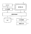
図1は、実施の形態による画像処理装置を備えた画像形成装置の機能的ブロック図である。画像形成装置は、スキャナ1、入力処理部2、操作表示部3、出力処理部4、画像出力部5、記憶部(HDD)6、および画像処理装置10を備える。
FIG. 1 is a functional block diagram of an image forming apparatus including an image processing apparatus according to an embodiment. The image forming apparatus includes a scanner 1, an input processing unit 2, an
スキャナ1は、原稿画像を読み取る。スキャナ1は、副走査方向に移動する原稿に読取光を照射し、その反射光をCCD(Charge Coupled Device)等の光電変換素子で光電変換することによって、当該原稿の画像を読み取る。スキャナ1は、搭載する複数枚の原稿を一枚ずつ送り出すADF(Auto Document Feeder)を備えている場合、ADFから送られてくる原稿を順次、アナログ画像データとして読み取って、このアナログ画像データを入力処理部2に送信する。 The scanner 1 reads a document image. The scanner 1 irradiates an original moving in the sub-scanning direction with reading light, and photoelectrically converts the reflected light by a photoelectric conversion element such as a CCD (Charge Coupled Device) to read an image of the original. When the scanner 1 includes an ADF (Auto Document Feeder) that sends out a plurality of documents to be mounted one by one, the document sent from the ADF is sequentially read as analog image data, and the analog image data is input. It transmits to the processing unit 2.
入力処理部2は、スキャナ1が読み取ったアナログデータを受信し、デジタル画像データに変換して記憶部6に出力して格納させ、それと共に、画像処理装置10に送信する。
The input processing unit 2 receives the analog data read by the scanner 1, converts it into digital image data, outputs it to the
操作表示部3は、プレビュー画像を表示し、また操作者による設定入力を受け付ける。操作表示部3は、スキャナ1による読み取り、入力処理部2による入力処理、操作表示部3によるプレビュー画像の表示、出力処理部4による画像の出力処理、および画像出力部5による画像の出力処理などの設定入力を受け付ける。また、操作表示部3は、各種の画像処理が施された場合、処理後の画像を表示する。
The
操作表示部3は、例えば、液晶ディスプレイ等が用いられ、液晶モニタの上部に、タッチパネルを配置して構成する。操作表示部3は、各種操作キー、および液晶ディスプレイ上に配設されたタッチパネルを有する。操作キーやタッチパネルからは、画像形成装置の操作を行うのに必要な各種操作が行われるとともに、特に、ユーザが印刷したい原稿に対する原稿画像の画像処理(画像加工)、印刷条件に関する設定、後処理に関する設定等の各種設定操作を受け付ける。
For example, a liquid crystal display or the like is used as the
操作表示部3は、読み取った画像に対する回転処理を施す要求入力を受け付ける。受け付けられる回転処理の要求は、例えば、時計回りに90度、180度、および270度である。あるいは、数値情報による入力を受け付ける構成とすることもできる。また、分度器様のアイコンを表示して、角度を接触入力で受け付ける構成とすることもできる。
The
画像処理装置10は、入力処理部2によって処理された画像データを受信し、操作表示部3によって受け付けられた回転処理の要求に従って、読み込んだ画像情報を2次元分布における矩形状の回転処理単位に分割して、回転処理を施し、回転処理後には分割された処理単位を合わせて1つとした画像情報として、操作表示部3における表示として出力する。また出力処理部4における画像出力として出力する。
The
出力処理部4は、画像処理装置10によって処理された画像に対して、受け付けられた処理設定に基づいて出力処理を施す。また、出力処理部4は、画像データに対してガンマ変換など各種の必要な画像処理を施す。
The
出力処理部4は、また、出力処理を施す際に、画像メモリから読み込んで処理を施し、出力する際に、実施の形態による画像処理装置10によって読み込み、および書き込みの制御を受ける構成とすることができる。
The
画像出力部5は、出力処理部4によって施された出力処理の設定に従って画像出力する。ここで、画像出力部5が施す出力処理は、出力用紙に画像形成して画像出力するだけでなく、ステープル処理、パンチ穴空け処理など、印刷後の後処理も含む。
The
記憶部6は、大容量のRAM(Random Access Memory)やハードディスク(HDD)等の大容量記憶媒体で構成され、スキャナ1が読み取った画像データをファイル毎に分類して格納する。
The
本発明の画像処理装置は、実施の形態においては回転処理を施す例について説明するが、画像の回転処理だけではなく、所定のブロックを処理単位とする画像処理であって処理後の画素値が主走査方向に所定の規則で並べられるものに対して、適用することができる。例えば、上記したように出力処理部4が出力処理する際に適用できる。また、入力処理部2において、例えば、γ補正処理を施す際に、一旦記憶部6に格納した画像ファイルを画像メモリに保持し、ここから読み込んで処理を施して再び画像メモリに格納するなどの処理の場合にも、適用することができる。
The image processing apparatus according to the present invention will be described with respect to an example in which rotation processing is performed in the embodiment. However, not only image rotation processing but also image processing using a predetermined block as a processing unit, The present invention can be applied to those arranged in a predetermined rule in the main scanning direction. For example, it can be applied when the
図2は、実施の形態による画像処理装置の機能的ブロック図である。画像処理装置10は、画像サイズ設定部11、回転角度設定部12、入力アドレス設定部13、出力アドレス設定部14、画像分割部15、入力アドレス生成部16、出力アドレス生成部17、メモリ18、入力部19、回転部20、および出力部21を備える。
FIG. 2 is a functional block diagram of the image processing apparatus according to the embodiment. The
画像サイズ設定部11は、入力処理部2が入力処理を施した画像データから、処理しようとする画像の画像サイズを設定する。ここで、画像データは1ページごとに処理を施す。
The image
回転角度設定部12は、操作表示部3から操作者が選択入力する画像の回転角度を、処理すべき画像データに設定する。
The rotation
入力アドレス設定部13は、メモリ18に格納された画像情報を回転処理する際に、入力部19が格納された画像情報1ページ分の全体を読み込む時のスタートアドレスを、設定する。入力アドレス設定部13は、入力した画像データの横幅および縦の長さの2つのパラメータを設定する。
When the image information stored in the
出力アドレス設定部14は、メモリ18に格納された画像情報が回転処理を施され、出力部21が出力する際に、画像情報1ページ分全体を書き込む時のスタートアドレスを設定する。出力アドレス設定部14は、メモリに書き込む際の画像データの横幅および縦の長さの2つのパラメータを設定する。
The output
画像分割部15は、画像サイズ設定部11によって設定された画像のサイズに従って、画像データに対応するメモリアドレスを、回転処理単位に従って分割する。ここでは、分割される回転処理単位は、横(主走査方向)が4バイト×4の16バイトであり、縦(副走査方向)が128ラインの正方領域とする。このように、従来の分割領域から比較すると相当に大きな領域であるので、主走査方向に最大で16バイト分をバースト転送することによって、個々の画素点に対応するメモリアドレスにアクセスする必要がないので、メモリアクセスを減らすことができる。本願発明は、さらに、この回転処理単位がメモリにアラインされていない場合に対しても適用できる。
The
入力アドレス生成部16は、画像分割部15によって分割処理された回転処理単位における読み込みアドレス、およびバースト量の情報を生成する。ここで、メモリ18は、少なくとも1ページ分の画像データを格納するものである。あるいは、メモリ18は、好適には、読み込みおよび書き込みの2ページ分以上の画像データを格納できる容量を有するものである。
The input
入力アドレス生成部16は、画像分割部15から回転処理単位における主走査方向の先頭アドレスを受信し、非アクセス量およびマスク量を演算し、先頭アドレスとバースト量の情報を入力部19に送信する。
The input
入力部19は、入力アドレス生成部16が生成する回転処理単位の1ラインの先頭アドレス、非アクセス量、およびバースト量に従って、メモリ18から画像情報を読み出す。ここで、回転処理単位における主走査方向の先頭アドレス情報を受け取って、非アクセス量だけ読み飛ばし、1ラインの残りをバーストアクセスすることによって、先頭アドレスより後で非アクセス量より後のメモリアクセスを停止する。続いて、回転処理単位における次のラインの先頭アドレス情報を受け取って、同様の読み込み処理を施す。回転処理単位ごとに、このような読み込み処理を施す。
The
回転部20は、SRAM(FFで構成されていても可能)であって、回転処理単位を含む大きさである。回転部20は、入力部19によって読み出された回転処理単位の画像情報を、回転処理を施した形で一時的に保持する。
The rotating
出力部21は、回転部20によって回転処理を施されて保持された状態の画像情報を、出力アドレス生成部17の生成する先頭アドレスによって書き込み、以降は回転処理単位の主走査方向に非アクセス量、マスク量、およびバースト量に基づいてバーストアクセスして1ライン分を書き込む。バーストアクセスして書き込む間は、メモリの読み込みがない。続いて、出力部21は、回転処理単位における次のラインの先頭アドレス情報を受け取って同様のバーストアクセスによる書き込み処理を施す。回転処理単位ごとに、このような書き込み処理を施す。
The
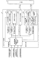
図3は、入力アドレス生成部16の機能的ブロック図である。入力アドレス生成部16は、回転処理単位の画素を読み込む際の、主走査方向のメモリ先頭アドレス情報、およびバースト長情報を生成する。また、先頭マスク量、および後端マスク量を生成して、入力部19がマスク処理を施す構成とすることもできる。
FIG. 3 is a functional block diagram of the input
入力アドレス生成部16は、転送量演算および次ラインの先頭アドレス生成部161、マスク生成部162、メモリアドレス生成部163、および非アクセス量演算部164を備える。
The input
転送量演算および次ラインの先頭アドレス生成部161は、入力アドレス生成部16の外部からは、画像サイズ設定部11から、分割前の画像の主走査長の情報を受信する。また、転送量演算および次ラインの先頭アドレス生成部161は、画像分割部15から分割後の回転処理単位における画像主走査長の情報を受信する。また、転送量演算および次ラインの先頭アドレス生成部161は、画像分割部15から分割後の回転処理単位における画像メモリ先頭アドレスの情報を受信する。また、転送量演算および次ラインの先頭アドレス生成部161は、画像分割部15から分割後の回転処理単位における画像副走査長の情報を受信する。
The transfer amount calculation and next line start
さらに、転送量演算および次ラインの先頭アドレス生成部161は、入力アドレス生成部16の内部からは、マスク生成部162からマスク情報を受信し、かつ非アクセス量演算部164からバースト長の情報を受信する。
Further, the transfer amount calculation and next-line head
マスク生成部162は、先頭マスク生成部162aおよび後端マスク生成部162bを有し、それぞれ先頭マスク量および後端マスク量の情報を生成する。
The
非アクセス量演算部164は、先頭非アクセス量演算部164a、後端非アクセス量演算部164b、およびバースト長演算部164cを有し、それぞれ先頭非アクセス量、後端非アクセス量、およびバースト長の情報を演算する。
The non-access
転送量演算および次ラインの先頭アドレス生成部161は、これらの情報から、転送量を演算し、演算結果の転送量の情報を、マスク生成部162、メモリアドレス生成部163、および非アクセス量演算部164に送信する。
The transfer amount calculation and next line start
メモリアドレス生成部163は、入力部19が読み出すべき回転処理単位の主走査方向のメモリ先頭アドレスの情報を生成して入力部19に送信する。
The memory
非アクセス量演算部164の有するバースト長演算部164cは、バースト長の情報を入力部19に送信する。
The burst
入力部19は、これら2つの情報によって、回転処理単位における1ライン分の主走査方向の先頭アドレスからメモリに対してバーストアクセスするため、メモリから高速にかつ効率的に読み込むことができる。
The
先頭マスク生成部162aは、メモリ先頭アドレスの情報を受信し、回転処理単位の副走査方向の先頭においてマスクすべきビットの情報を転送量演算および次ラインの先頭アドレス生成部161に送信する。マスクすることによって、アラインされていない部分を見掛け上データの無い状態として読み込む。ここでは、マスク処理を施すのは、書き込み処理の場合だけでよい。
The head
先頭非アクセス量演算部164aは、先頭部分のアラインされていない部分の情報のうち、主走査方向にマスクせずに読み飛ばすべき量を演算する。後端非アクセス量演算部164bは、後端部分のアラインされていない部分の情報のうち、主走査方向にマスクせずに読み飛ばすべき量を演算する。入力部19は、これによって、アラインされていない部分のうち、非アクセス量だけ読み飛ばすことによって、メモリアクセスおよび画素値の読み込み無しに、入力処理を行うことができる。
The head non-access amount calculation unit 164a calculates the amount of information to be skipped without masking in the main scanning direction from the information of the unaligned portion of the head portion. The rear end non-access amount calculation unit 164b calculates the amount to be skipped without masking in the main scanning direction from the information of the unaligned portion of the rear end portion. Accordingly, the
バースト長演算部164cは、メモリ先頭アドレスを読み込んで読み飛ばした後、メモリアドレスを読み込まずに主走査方向にバーストアクセスするバースト長を演算する。バースト長演算部164cによって演算されたバースト長の情報は、入力部19に送信される。入力部19は、これによって、必要なバースト長だけメモリアクセスすることによって効率的に読み込むことができる。
The burst
入力部19は、回転処理単位における1ライン分の先頭アドレスに従って、回転処理単位の主走査方向の先頭アドレスに対応する画素値を読み出し、そのまま、必要なバースト長分だけバーストアクセスして画素値を読み出す。アラインされたメモリアドレスから実際に必要な画像の存在するアドレスまでは、メモリにアクセスすることがないため、メモリアクセス時間を短縮することができる。そして、回転処理単位内で主走査方向にバースト長だけ読み込んだ後、回転処理単位内でアクセスされていない副走査方向のラインがあった場合は、入力アドレス生成部16が生成する次のラインの先頭アドレスを受信して、受信した先頭アドレスに従って、上記と同様のバーストアクセスを行う。このようにして、主走査方向のアクセスを順次繰り返すことによって、回転処理単位内の画素データをバーストアクセスによって読み込む。
The
図4は、入力部によるメモリへのバーストアクセスを説明する模式図である。2次元のメモリ上に分布する画素に対応するメモリアドレス400は、回転処理単位を格子単位として格子状に分割されている。ここで、格子の縦のラインは、下位4ビットが0のものを取っている。記号では図中[3:0]=0で表現されるアドレスが縦のラインである。 FIG. 4 is a schematic diagram illustrating burst access to the memory by the input unit. The memory addresses 400 corresponding to the pixels distributed on the two-dimensional memory are divided into a lattice shape with the rotation processing unit as a lattice unit. Here, the vertical lines of the lattice are those whose lower 4 bits are 0. In the symbol, the address represented by [3: 0] = 0 in the figure is a vertical line.
ここでは、回転処理単位は、16バイトを主走査方向幅とし、副走査方向に128本のラインで構成する。回転処理単位は例えば、図中符号420などで表現されるように、1つの格子で囲まれた領域である。ここで、矩形状の画像データに対応するメモリ領域451は、画像データの頂点431に見るように、入力先頭アドレスが回転処理単位にアラインされていない。即ち、領域430および450はアラインされていない。それに対して、領域420などはアラインされている。
Here, the rotation processing unit is 16 bytes in the main scanning direction width, and is composed of 128 lines in the sub-scanning direction. The rotation processing unit is, for example, an area surrounded by one grid as represented by
今、アドレスデータ451は、領域450のある主走査方向1ライン分の画像データを取り出して、模式的に示したもので、16バイトを主走査方向に模式的に表現している。このアドレスデータ451は、先頭アドレスが回転処理単位にアラインされていないので、先頭から8バイトまではメモリアクセス無し(符号452)とする。そして、続く9バイト目からの4バイトでは、このバイト内において途中から画素値が始まるので、該途中までの1バイトに対してマスク処理を施す(符号453)。そして、3バイト分の有効データ部分および残りのマスク無しの4バイト分の有効データ(符号454)が続く。実際上の画素値にアクセスするのは、マスク453の部分以降である。
The
従って、データ451においては、メモリアクセス無しに読み飛ばし、入力先頭アドレスをデータ453とし、データ453においてマスク処理を施し、それ以降の有効データ454についてはバーストアクセスして読み込む。
Accordingly, the
図5は、回転部20が画像処理単位の画素値に回転処理を施すことを説明する図である。回転部20は例えばSRAMによって構成し、回転処理単位に対応する画素値を、回転処理単位の主走査方向1ラインについて読み込んで保持する。即ち、最初のラインとしてP11、P12、……、P1n、次のラインとしてP21、P22、……、最後の画素点としてPnnを読み込んで保持する。これをマトリクス表現したのが表510である。
FIG. 5 is a diagram for explaining that the
回転部20は、回転角度設定部12によって設定された回転角度に従って、画像情報に回転処理を施す。この格納された画素点について、設定された角度、例えば90度回転処理を施して、回転後の画素を模式的に表現する表550を得る。ここでは主走査方向に、Pn1、……P21、P11が配列され保持される。
The
出力部21は、出力アドレス生成部17が生成する出力先頭アドレス、非アクセス量情報、マスク量情報、およびバースト長情報によって、回転部20によって回転された画素情報をバースト書き込み処理する。
The
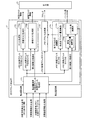
図6は、出力アドレス生成部17の機能的ブロック図である。出力アドレス生成部17は、転送量演算および次ラインの先頭アドレス生成部171、マスク生成部172、メモリアドレス生成部173、および非アクセス量演算部174を備える。
FIG. 6 is a functional block diagram of the output
転送量演算および次ラインの先頭アドレス生成部171は、入力アドレス生成部16の時と同様に、画像サイズ設定部11から分割前の画像の主走査長の情報を受信する。また、画像分割部15から、分割後の画像主走査長の情報を受信する。また、画像分割部15から、分割後画像メモリの先頭アドレスの情報を受信する。また、画像分割部15から、分割後の画像副走査長の情報を受信する。
Similarly to the case of the input
さらに、転送量演算および次ラインの先頭アドレス生成部171は、マスク生成部172からマスク情報を受信し、かつ非アクセス量演算部174から、非アクセス量情報およびバースト長の情報を受信する。
Further, the transfer amount calculation and next line start address generation unit 171 receives mask information from the
転送量演算および次ラインの先頭アドレス生成部171は、これらの情報から転送量を演算し、演算結果の転送量の情報をマスク生成部172、メモリアドレス生成部173、および非アクセス量演算部174に送信する。
The transfer amount calculation and start address generation unit 171 of the next line calculates the transfer amount from these pieces of information, and uses the information on the transfer amount of the calculation result as a
メモリアドレス生成部173は、出力部21がメモリに書き込むべきメモリ先頭アドレスの情報を出力部21に送信し、非アクセス量演算部174aが演算する非アクセス量、およびバースト長演算部174cが演算するバースト長の情報を、出力部21に送信する。
The memory
ここで、マスク生成部172は、先頭マスク生成部172a、および後端マスク生成部172bを有する。先頭マスク生成部172aは、メモリ先頭アドレスの情報を受信し、回転処理単位の主走査方向の先頭においてマスクするビット情報を転送量演算および次ラインの先頭アドレス生成部171に送信する。また、先頭マスク生成部172aは、先頭においてマスクするビットの情報を出力部21に送信する。出力部21は、書き込みにおいてマスクすることによって、先端において有効でない画素データの書き込みを停止する。
Here, the
後端マスク生成部172bは、残り画像主走査長の情報を受信し、回転処理単位の主走査方向の後端においてマスクするビットの情報を転送量演算および次ラインの先頭アドレス生成部171に送信する。また、後端マスク生成部172bは、後端においてマスクするビット情報を出力部21に送信する。出力部21は、書き込みにおいてマスクすることによって、後端において有効でない画素データの書き込みを停止する。
The rear end
メモリアドレス生成部173は、回転処理単位における主走査方向のメモリ先頭アドレスの情報を生成して出力部21に送信する。
The memory
非アクセス量演算部174は、先頭非アクセス量演算部174a、後端非アクセス量演算部174b、およびバースト長演算部174cを有し、それぞれ先頭非アクセス量、後端非アクセス量、およびバースト長の情報を、演算する。
The non-access
先頭非アクセス量演算部174aは、先頭部分のアラインされていない部分の情報のうち、マスクせずに書き飛ばすべき量を演算する。後端非アクセス量演算部174bは、後端部分のアラインされていない部分の情報のうち、マスクせずに書き飛ばすべき量を演算する。バースト長演算部174cは、書き飛ばすべき量を加算後のメモリアドレスから主走査長によって決定される後端までのバースト数を演算する。バースト長演算部174cによって演算されたバースト長の情報は出力部21に送信される。
The head non-access
出力部21は、出力アドレス生成部17によって生成される先頭アドレス、先頭非アクセス量、先頭マスク情報、バースト長、後端マスク情報、および後端非アクセス量に従って、画像情報をメモリに書き込む。即ち、出力部21は、先頭非アクセス量分のアドレスを加算後のアドレスから、先頭マスク情報、および後端非アクセス量、後端マスク量の情報に従って、書き飛ばしながら、該マスク量だけマスクしつつ、バースト長分の情報を書き込む。
The
このようにして、出力部21は、バーストアクセスして画素情報を書き込む間は、先頭アドレスを出力後、連続した領域に続けて画像データを書き込むので、メモリアクセスを省略できる。そして、回転処理単位内で主走査方向にバースト長だけ書き込んだ後は、同じ回転処理単位内にアクセスされていない次の主走査方向のラインがあった場合は、上記と同様のバーストアクセスを行ってメモリ18に書き込む。このようにして、主走査方向のバーストアクセスによる書き込み処理を順次施すことによって、回転処理された回転処理単位ごとの画素データを出力する。
In this manner, the
ここで、メモリ空間において回転処理単位が格子にアラインしている場合は、読み飛ばし処理およびマスク処理の必要は生じない。メモリ先頭アドレスに従って、回転処理単位の主走査方向の幅だけ書き込むことができる。 Here, when the rotation processing unit is aligned with the lattice in the memory space, there is no need for skip processing and mask processing. Only the width in the main scanning direction of the rotation processing unit can be written according to the memory head address.
図7は、実施の形態による入力アドレス生成手順を説明するフローチャートである。入力アドレス生成部16において、転送量演算および次ラインの先頭アドレス生成部161は、最初、分割前の画像主走査長、分割後の画像主走査長、画像メモリ先頭アドレス、および画像副走査長の情報を受信する(ステップS101)。転送量演算および次ラインの先頭アドレス生成部161は、受信したこれらの情報から、メモリ先頭アドレス、および残り画像主走査長を演算する(ステップS102)。
FIG. 7 is a flowchart for explaining an input address generation procedure according to the embodiment. In the input
非アクセス量演算部164は、先端非アクセス量、および後端非アクセス量を演算する(ステップS103)。図4に示したメモリアクセス無し領域(符号452)が先端非アクセス量に相当する部分である。後端非アクセス量は、後端においてアラインされてない領域があった場合に、発生することがあるが、先端と同様であるので説明を省略する。
The non-access
メモリアドレス生成部163は、回転処理単位における主走査方向の読み込み先頭アドレスを生成して入力部19へ送信する(ステップS104)。
The memory
一方、マスク生成部162は、先頭マスク量および後端マスク量を生成する(ステップS105)。図4に示したマスク領域(符号453)が先頭マスク量に相当する部分である。後端マスク量は、後端においてアラインされてない領域があった場合に、発生することがあるが、先端と同様であるので説明を省略する。
On the other hand, the
バースト長演算部164cは、バースト長を演算し入力部19へ送信する(ステップS106)。バースト量は、一般に、先端アドレスより後で、回転処理単位における後端までの間である。この間は、入力部19においては、バースト開始アドレス出力後、連続領域に対して一気にバーストアクセスすることができる。
The burst
転送量演算および次ラインの先頭アドレス生成部161は、回転処理単位内で処理は完了したか否かを判定し(ステップS107)、完了しなかったと判定した場合(ステップS107のNo)、ステップS102に戻る。アクセスされていない次のラインについて読み込むために、上記と同様のステップを繰り返す。この時、回転処理単位における最初のラインではないので、演算して取得した各情報をフィードバックする(ステップS102)。
The transfer amount calculation and head
一方、回転処理単位内での処理が完了したと判定した場合は(ステップS107のYes)、転送量演算および次ラインの先頭アドレス生成部161は、1ページ分の回転処理が終了したか否かを判定する(ステップS108)。1ページ分の回転処理が終了したと判定した場合(ステップS108のYes)、そのまま終了する。1ページ分の回転処理が終了していないと判定した場合(ステップS108のNo)、再びステップS101に戻って、アクセスされていない回転処理単位について同様の処理を繰り返す。
On the other hand, if it is determined that the processing within the rotation processing unit has been completed (Yes in step S107), the transfer amount calculation and next line head
図8は、実施の形態による出力アドレス生成手順を説明するフローチャートである。出力アドレス生成部17において、転送量演算および次ラインの先頭アドレス生成部171は、分割前の画像主走査長、分割後の画像主走査長、画像メモリ先頭アドレス、および画像副走査長の情報を受信する(ステップS201)。転送量演算および次ラインの先頭アドレス生成部171は、メモリ先頭アドレス、および残り画像主走査長を演算する(ステップS202)。
FIG. 8 is a flowchart for explaining an output address generation procedure according to the embodiment. In the output
非アクセス量演算部174は、先端非アクセス量および後端非アクセス量を演算する(ステップS203)。図4に示した入力データの模式図をそのまま回転処理を施した出力データの模式図として見ると、メモリアクセス無し領域(符号452)が先端非アクセス量に相当する部分である。後端非アクセス量は、後端においてアラインされてない領域があった場合に、発生することがあるが、先端と同様であるので説明を省略する。
The non-access
メモリアドレス生成部173は、書き込み先頭アドレスを生成して出力部へ送信する(ステップS204)。
The memory
マスク生成部172は、先頭マスク量および後端マスク量を生成する(ステップS205)。マスク生成部172は、生成した先頭マスク量および後端マスク量を出力部21へ送信する(ステップS206)。ここで、出力部21は、受信した先頭マスク量、および後端マスク量に相当する画素については、マスク処理を施して出力するので、見掛け上は書き込み処理を施さない。
The
バースト長演算部174cは、バースト長を演算し出力部21へ送信する(ステップS207)。出力部21は、非アクセス量を受信してアラインしていない部分を非アクセス量に従って書き飛ばして書き込みを停止し、先頭マスク量を受信して受信した先頭マスク量に相当する部分にマスク処理を施し、その後において、バースト長に基づいて画素値をバーストアクセスして書き込む。そして、後端マスク処理を施し、その後、後端において非アクセス量の情報に従って、書き飛ばし処理を施す。
The burst
転送量演算および次ラインの先頭アドレス生成部171は、回転処理単位内で処理は完了したか否かを判定し(ステップS208)、完了していないと判定した場合(ステップS208のNo)、ステップ202に戻る。完了したと判定した場合(ステップS208のYes)、転送量演算および次ラインの先頭アドレス生成部171は、さらに1ページ分の回転処理が終了したか否かを判定し(ステップS209)、終了していないと判定した場合(ステップS209のNo)、ステップ201に戻り、終了したと判定した場合(ステップS209のYes)、このページの画像の回転処理を終了する。 The transfer amount calculation and head address generation unit 171 of the next line determines whether or not the process is completed within the rotation processing unit (step S208). If it is determined that the process is not completed (No in step S208), the process proceeds to step S208. Return to 202. When it is determined that the transfer has been completed (Yes in step S208), the transfer amount calculation and next-line head address generation unit 171 determines whether or not the rotation processing for one page has been completed (step S209), and the processing ends. If it is determined that it has not (No in step S209), the process returns to step 201, and if it is determined that the process has ended (Yes in step S209), the image rotation processing on this page ends.
図9は、従来例による画像処理装置と、実施の形態による画像処理装置との画像処理におけるメモリアクセスを説明する図である。図9におけるデータ910は、特許文献1の技術によって、主走査方向16バイトのデータに対してバーストアクセスした場合の態様である。ここでは、アラインしていない回転処理単位の先頭アドレス([1:0]が0でない場合)をアラインさせて[1:0]=0とし、不必要な部分をマスク処理する。マスクされた領域が符号911で示した部分である。その後に有効データ912が続く。しかし、ここでマスク領域911も実際には入力部19が読み込んで、書き込みにおいてマスク処理を施しているため、無駄な読み込みが発生している。
FIG. 9 is a diagram for explaining memory access in image processing between the image processing apparatus according to the conventional example and the image processing apparatus according to the embodiment.
一方、図9におけるデータ950は、実施の形態による技術を16バイトデータに対するバーストアクセスに適用した場合の処理の態様である。ここでは、不必要な画素に対して、メモリアクセス無しの領域951を設定し、その後において必要な部分のみをマスク処理し(符号952)、その後に有効データ953が続く。このため、メモリアクセス無しの領域951の部分は、読み込みを停止して、マスク部分を少なくすることができるので、結局、無駄な読み込みを停止させ、画像処理効率が従来例よりも優れたものとなっている。
On the other hand,
また、従来例においては、回転処理単位を小さく設定して読み込みの無駄を排する場合は、小さく設定した回転処理単位によってバーストアクセスできるバースト長が小さいものとなり、メモリへのアクセスの回数が増加して画像処理効率が高いものとは成らない。これに対して、実施の形態による画像処理装置10では、回転処理単位を小さく設定する必要が無く、無駄なメモリアクセスを排除することができる。また、回転処理単位を大きく設定すればするほどバースト長を長くとれるので、メモリアクセス数をさらに減少させることができ、画像処理効率は優れたものとすることができる。
In addition, in the conventional example, when the rotation processing unit is set to be small and waste of reading is eliminated, the burst length that can be burst-accessed by the rotation processing unit that is set small is small, and the number of accesses to the memory increases. Therefore, the image processing efficiency is not high. On the other hand, in the
このようにして、実施の形態による画像処理装置は、画像情報を読み込み回転処理単位に分割して回転処理を施す際に、回転処理単位の先頭アドレスとバースト長とを取得して、先頭アドレスのみ出力し、それより後の主走査方向についてはバースト転送することによって、無駄なメモリアクセスを減らして画像の回転速度の低下を最小限に抑えることができる。 As described above, when the image processing apparatus according to the embodiment reads the image information and divides it into rotation processing units and performs rotation processing, the image processing device acquires the start address and burst length of the rotation processing unit, and only the head address is acquired. By outputting and performing burst transfer in the main scanning direction after that, it is possible to reduce useless memory access and minimize a decrease in image rotation speed.
また、2次元で規定されるアドレスの所定の格子と、先頭アドレスとがアラインしない回転処理単位に対しては、メモリアクセスしない部分を設定し、先頭アドレスを決定し、不要なデータについては読み飛ばし、必要なビット数だけマスクして、バースト転送することによって、回転前画像と回転後画像のスタートアドレスをバイト単位で設定でき、かつバースト転送することによって無駄なメモリアクセスを減らして画像の回転処理において回転速度の低下を最小限に抑えることができる。 In addition, for a rotation processing unit in which a predetermined grid of addresses defined in two dimensions and the start address are not aligned, a portion where no memory is accessed is set, the start address is determined, and unnecessary data is skipped. By masking only the required number of bits and performing burst transfer, the start address of the pre-rotation image and post-rotation image can be set in bytes, and burst transfer reduces the unnecessary memory access and rotates the image. In this case, a decrease in rotational speed can be minimized.
(変形例1)
実施の形態による画像処理装置は、画像形成装置に適用されたものとして説明した。しかしながら、本発明の画像処理装置は、画像形成装置にのみ適用できるものではなく、画像データを少なくとも一時的に格納して読み込み、他のメモリに書き込む画像処理を必要とする装置には適用可能である。例えば、文字画像を含む画像を受信して、回転させ、あるいは何らかの画像処理を施して表示画面に表示する携帯電話における画像処理装置としても適用可能である。
(Modification 1)
The image processing apparatus according to the embodiment has been described as applied to an image forming apparatus. However, the image processing apparatus of the present invention is not applicable only to an image forming apparatus, but can be applied to an apparatus that requires image processing to store and read image data at least temporarily and write it to another memory. is there. For example, the present invention can also be applied as an image processing apparatus in a mobile phone that receives an image including a character image, rotates it, or performs some image processing and displays it on a display screen.
(変形例2)
他の変形例としては、例えば、CCD(ChargeCoupledDevice)を介して被写体画像を取り込み、回転させ、あるいは何らかの画像処理を施して表示画面に表示するデジタル方式のカメラにおける画像処理装置としても適用可能である。
(Modification 2)
As another modification, for example, the present invention can be applied as an image processing apparatus in a digital camera that captures a subject image via a CCD (ChargeCoupled Device), rotates the image, or performs some image processing and displays the image on a display screen. .
(変形例3)
さらに他の変形例としては、例えば、文字画像を含む画像を読み込んで、回転させ、あるいは何らかの画像処理を施してモニタ画面に表示するパーソナルコンピュータ(PC)における画像処理プログラムとしても適用可能である。
(Modification 3)
As another modification, for example, the present invention can be applied as an image processing program in a personal computer (PC) that reads an image including a character image, rotates it, or performs some image processing and displays it on a monitor screen.
(ハードウェア構成など)
図10は、実施の形態による画像処理装置を備えた画像形成装置のハードウェア構成を示すブロック図である。この画像形成装置は、ファックスやスキャナなどの複合的機能を備える複合機(MFP)として構成されている。図に示すように、このMFPは、コントローラ2210とエンジン部2260とをPCI(Peripheral Component Interconnect)バスで接続した構成となる。コントローラ2210は、MFP全体の制御、画像表示制御、各種制御、画像処理制御など、FCUI/F2230、操作表示部3からの入力を制御するコントローラである。エンジン部2260は、PCIバスに接続可能な画像処理エンジンなどであり、例えば取得した画像データに対して誤差拡散やガンマ変換などの画像処理部分が含まれる。
(Hardware configuration etc.)
FIG. 10 is a block diagram illustrating a hardware configuration of an image forming apparatus including the image processing apparatus according to the embodiment. This image forming apparatus is configured as a multifunction peripheral (MFP) having multiple functions such as a fax machine and a scanner. As shown in the figure, this MFP has a configuration in which a
コントローラ2210は、CPU2211と、ノースブリッジ(NB)2213と、システムメモリ(MEM−P)2212と、サウスブリッジ(SB)2214と、ローカルメモリ(MEM−C)2217と、ASIC(Application Specific Integrated Circuit)2216と、ハードディスクドライブ6とを有し、ノースブリッジ2213とASIC2216との間をAGP(Accelerated Graphics Port)バス2215で接続した構成となる。また、MEM−P2212は、ROM(Read Only Memory)2212aと、RAM(Random Access Memory)2212bとをさらに有する。
The
CPU2211は、MFPの全体制御を行うものであり、NB2213、MEM−P2212およびSB2214からなるチップセットを有し、このチップセットを介して他の機器と接続される。
The
NB2213は、CPU2211とMEM−P2212、SB2214、AGP2215とを接続するためのブリッジであり、MEM−P2212に対する読み書きなどを制御するメモリコントローラと、PCIマスタおよびAGPターゲットとを有する。
The
MEM−P2212は、プログラムやデータの格納用メモリ、プログラムやデータの展開用メモリなどとして用いるシステムメモリであり、ROM2212aとRAM2212bとからなる。ROM2212aは、プログラムやデータの格納用メモリとして用いる読み出し専用のメモリであり、RAM2212bは、プログラムやデータの展開用メモリ、画像処理時の画像描画メモリなどとして用いる書き込みおよび読み出し可能なメモリである。
The MEM-
SB2214は、NB2213とPCIデバイス、周辺デバイスとを接続するためのブリッジである。このSB2214は、PCIバスを介してNB2213と接続されており、このPCIバスには、FCUI/F2230なども接続される。
The
ASIC2216は、マルチメディア情報処理用のハードウェア要素を有するマルチメディア情報処理用途向けのIC(Integrated Circuit)であり、AGP2215、PCIバス、HDD6およびMEM−C2217をそれぞれ接続するブリッジの役割を有する。
The
このASIC2216は、PCIターゲットおよびAGPマスタと、ASIC2216の中核をなすアービタ(ARB)と、MEM−C2217を制御するメモリコントローラと、ハードウェアロジック等により画像データの回転などを行う複数のDMAC(Direct Memory Access Controller)と、エンジン部2260との間でPCIバスを介してUSB(Universal Serial Bus)2240、IEEE(the Institute of Electrical and Electronics Engineers)1394インタフェース2250が接続される。
The
MEM−C2217は、送信用画像バッファ、符号バッファとして用いるローカルメモリであり、HDD6は、画像データの蓄積、プログラムの蓄積、フォントデータの蓄積、フォームの蓄積を行うためのストーレジである。
The MEM-
AGP2215は、グラフィック処理を高速化するために提案されたグラフィックスアクセラレータカード用のバスインタフェースであり、MEM−P2212に高スループットで直接アクセスすることにより、グラフィクスアクセラレータカードを高速にするものである。
The
ASIC2216に接続する操作表示部3は、操作者からの操作入力を受け付けて、ASIC2216に受け付けられた操作入力情報を送信する。
The
なお、実施の形態による画像処理装置を組み込んだMFPで実行される画像処理プログラムは、ROM等に予め組み込まれて提供される。 An image processing program executed by the MFP in which the image processing apparatus according to the embodiment is incorporated is provided by being incorporated in advance in a ROM or the like.
実施の形態による画像処理装置を組み込んだMFPで実行される画像処理プログラムは、インストール可能な形式又は実行可能な形式のファイルでCD−ROM、フレキシブルディスク(FD)、CD−R、DVD(Digital Versatile Disk)等のコンピュータで読み取り可能な記録媒体に記録して提供するように構成してもよい。 An image processing program executed by an MFP incorporating the image processing apparatus according to the embodiment is a file in an installable format or an executable format, and is a CD-ROM, a flexible disk (FD), a CD-R, a DVD (Digital Versatile). It may be configured to be recorded on a computer-readable recording medium such as Disk).
さらに、実施の形態による画像処理装置を組み込んだMFPで実行される画像処理プログラムを、インターネット等のネットワークに接続されたコンピュータ上に格納し、ネットワーク経由でダウンロードさせることにより提供するように構成しても良い。また、実施の形態による画像処理装置を組み込んだMFPで実行される画像処理プログラムをインターネット等のネットワーク経由で提供または配布するように構成しても良い。 Further, the image processing program executed by the MFP incorporating the image processing apparatus according to the embodiment is stored on a computer connected to a network such as the Internet, and is provided by being downloaded via the network. Also good. Further, the image processing program executed by the MFP incorporating the image processing apparatus according to the embodiment may be provided or distributed via a network such as the Internet.
実施の形態による画像処理装置を組み込んだMFPで実行される画像処理プログラムは、上述した各部(画像サイズ設定部11、回転角度設定部12、入力アドレス設定部13、出力アドレス設定部14、画像分割部15、入力アドレス生成部16、出力アドレス生成部17、入力部19、回転部20、出力部21など)を含むモジュール構成となっており、実際のハードウェアとしてはCPU(プロセッサ)が上記ROMから画像表示プログラムを読み出して実行することにより上記各部が主記憶装置上に、画像サイズ設定部11、回転角度設定部12、入力アドレス設定部13、出力アドレス設定部14、画像分割部15、入力アドレス生成部16、出力アドレス生成部17、入力部19、回転部20、出力部21などが主記憶装置上に生成されるようになっている。
The image processing program executed by the MFP incorporating the image processing apparatus according to the embodiment includes the above-described units (image
以上説明した本発明の実施の形態あるいは変形例は、説明のための一例であって、本発明はここに説明したこれらの具体例に限定されるものではない。 The embodiment or modification of the present invention described above is an example for description, and the present invention is not limited to these specific examples described here.
以上のように、本発明にかかる画像処理装置、画像処理方法、その方法をコンピュータに実行させるプログラムは、画像処理技術に有用であり、特に、記憶装置から画像データを読み出して処理を施す画像処理技術に適している。 As described above, the image processing apparatus, the image processing method, and the program for causing the computer to execute the method according to the present invention are useful for the image processing technology, and in particular, the image processing that reads and processes the image data from the storage device. Suitable for technology.
1 スキャナ
2 入力処理部
3 操作表示部
4 出力処理部
5 画像出力部
6 記憶部(HDD)
10 画像処理装置
11 画像サイズ設定部
12 回転角度設定部
13 入力アドレス設定部
14 出力アドレス設定部
15 画像分割部
16 入力アドレス生成部
17 出力アドレス生成部
18 メモリ
19 入力部
20 回転部
21 出力部
DESCRIPTION OF SYMBOLS 1 Scanner 2
DESCRIPTION OF
Claims (13)
前記画像メモリから前記画像データを読み出す入力メモリアドレスを生成する入力アドレス生成手段と、
前記入力アドレス生成手段によって生成された入力メモリアドレスに基づいて、前記画像メモリにバーストアクセスして、画像データを読み出すメモリアクセス制御手段と、
前記入力アドレス生成手段によって生成された入力アドレスに基づいて前記画像データを読み込んで回転処理を施す回転処理手段と、を備え、
前記入力アドレス生成手段は、
前記画像メモリに格納された画像データを読み出す主走査方向の先頭メモリアドレスであって前記分割手段によって分割された矩形領域の先頭アドレスを生成する先頭メモリアドレス生成手段、および、
主走査方向の所定幅における先頭画素からの非アクセス量である先頭非アクセス量、前記主走査方向の所定幅における後端画素に至るまでの非アクセス量である後端非アクセス量、及び前記メモリアクセス制御手段がバーストアクセスする前記矩形領域内におけるバースト長を演算することにより、前記先頭メモリアドレス生成手段によって生成された先頭アドレスに対応する画素以降の読み込みを停止する画素数を演算する非アクセス量演算手段を、有し、
前記メモリアクセス制御手段は、前記先頭アドレスに対応する画素以降、前記非アクセス量演算手段によって前記先頭非アクセス量、前記後端非アクセス量、および前記バースト長に基づいて演算された画素数の画像データを読み飛ばして前記画像メモリにバーストアクセスし、格納された画像データを読み出し、前記回転処理手段によって回転処理を施された画像データを、前記画像メモリにバースト転送するものであることを特徴とする画像処理装置。 A dividing means for dividing an image memory for storing image data into rectangular areas;
An input address generating means for generating an input memory address to read out the image data from the image memory,
Memory access control means for performing burst access to the image memory and reading out image data based on the input memory address generated by the input address generation means;
Rotation processing means that reads the image data based on the input address generated by the input address generation means and performs rotation processing;
The input address generating means
Head memory address generating means for generating a head address of a rectangular area divided by the dividing means, which is a head memory address in the main scanning direction for reading out image data stored in the image memory; and
A head non-access amount that is a non-access amount from the top pixel in a predetermined width in the main scanning direction, a rear end non-access amount that is a non-access amount up to a rear end pixel in the predetermined width in the main scanning direction, and the memory by access control means for calculating a burst length in the rectangular region to burst access, non for calculating the number of pixels to stop reading the subsequent pixels corresponding to the previously Atamaa dress generated by the first memory address generating means Having access amount calculation means,
Said memory access control means, said destination Atamaa subsequent pixels corresponding to the dress, the top non-access amount by said non-access amount calculating means, the rear end non-access volume, and number of pixels that have been calculated based on the burst length The image data is skipped, the image memory is burst accessed, the stored image data is read, and the image data subjected to the rotation processing by the rotation processing means is burst transferred to the image memory. A featured image processing apparatus.
前記メモリアクセス制御手段は、前記出力アドレス生成手段によって生成された出力メモリアドレスに基づいて、読み出した前記画像データを、前記画像メモリにバースト転送するものであることを特徴とする請求項1に記載の画像処理装置。 Output address generation means for generating an output memory address for storing the image data read out by the image memory access control means in an image memory;
It said memory access control means on the basis of the output memory address generated by the output address generating means, the image data read out, according to claim 1, characterized in that the image memory is to burst transfer Image processing apparatus.
上記先頭読み飛ばしに後続する所定の画素数だけマスク処理を施す先頭マスク生成手段、および、
上記後端読み飛ばしに先行する所定の画素数だけマスク処理を施す後端マスク生成手段を有し、
前記先頭マスク生成手段によるマスク処理、および前記後端マスク生成手段によるマスク処理によって、前記画像データに対してマスク処理を施すものであることを特徴とする請求項4に記載の画像処理装置。 The mask generating means includes
A head mask generating means for performing mask processing for a predetermined number of pixels following the head reading skip; and
Rear end mask generating means for performing mask processing for a predetermined number of pixels preceding the rear end skipping,
The image processing apparatus according to claim 4 , wherein the image data is subjected to mask processing by mask processing by the leading mask generation unit and mask processing by the trailing edge mask generation unit.
分割手段によって、画像データを格納する画像メモリを矩形領域に分割する分割工程と、
入力アドレス生成手段によって、前記画像メモリから前記画像データを読み出す入力メモリアドレスを生成する入力アドレス生成工程と、
メモリアクセス制御手段によって、前記入力アドレス生成工程で生成された入力メモリアドレスに基づいて、前記画像メモリにバーストアクセスして、画像データを読み出すメモリアクセス制御工程と、
回転処理手段によって、前記入力アドレス生成工程で生成された入力アドレスに基づいて前記画像データを読み込んで回転処理を施す回転処理工程と、を含み、
前記入力アドレス生成工程は、
先頭メモリアドレス生成手段によって、前記画像メモリに格納された画像データを読み出す主走査方向の先頭メモリアドレスであって前記分割工程で分割された矩形領域の先頭アドレスを生成する先頭メモリアドレス生成工程、および、
非アクセス量演算手段によって、主走査方向の所定幅における先頭画素からの非アクセス量である先頭非アクセス量、前記主走査方向の所定幅における後端画素に至るまでの非アクセス量である後端非アクセス量、及び前記メモリアクセス制御手段がバーストアクセスする前記矩形領域内におけるバースト長を演算することにより、前記先頭メモリアドレス生成工程で生成された先頭アドレスに対応する画素以降の読み込みを停止する画素数を演算する非アクセス量演算工程を、含み、
前記メモリアクセス制御工程は、前記先頭アドレスに対応する画素以降、前記非アクセス量演算工程で前記先頭非アクセス量、前記後端非アクセス量、および前記バースト長に基づいて演算された画素数の画像データを読み飛ばして前記画像メモリにバーストアクセスし、格納された画像データを読み出し、前記回転処理工程で回転処理を施された画像データを、前記画像メモリにバースト転送するものであることを特徴とする画像処理方法。 An image processing method in an image processing apparatus,
A dividing step of dividing the image memory storing the image data into rectangular areas by a dividing unit;
By the input address generating unit, an input address generating step of generating an input memory address to read out the image data from the image memory,
Based on the input memory address generated in the input address generation step by the memory access control means, a memory access control step of performing burst access to the image memory and reading out image data;
A rotation processing step by which the rotation processing means reads the image data based on the input address generated in the input address generation step and performs the rotation processing;
The input address generation step includes
A leading memory address generating step for generating a leading memory address in the main scanning direction for reading out image data stored in the image memory by a leading memory address generating means, and generating a leading address of the rectangular area divided in the dividing step; and ,
The leading non-access amount that is the non-access amount from the leading pixel in the predetermined width in the main scanning direction by the non-access amount calculating means, and the trailing edge that is the non-accessing amount up to the trailing pixel in the predetermined width in the main scanning direction non-access volume, and the by the memory access control means for calculating a burst length within the rectangular area to be burst access, stops reading of the subsequent pixel corresponding to the first memory address generating step in the generated previously Atamaa dress A non-access amount calculation step for calculating the number of pixels to be performed,
Said memory access control step, the destination Atamaa subsequent pixels corresponding to the dress, the top non-access amount by said non-access quantity calculation step, the rear end non-access volume, and number of pixels that have been calculated based on the burst length The image data is skipped, the image memory is burst-accessed, the stored image data is read, and the image data subjected to the rotation process in the rotation process step is burst-transferred to the image memory. A featured image processing method.
前記メモリアクセス制御工程は、前記メモリアクセス制御手段が、前記出力アドレス生成工程で生成された出力メモリアドレスに基づいて、読み出した前記画像データを、前記画像メモリにバースト転送するものであることを特徴とする請求項7に記載の画像処理方法。 An output address generation step of generating an output memory address for storing the image data read in the image memory access control step by the output address generation means in the image memory;
In the memory access control step, the memory access control means performs burst transfer of the read image data to the image memory based on the output memory address generated in the output address generation step. The image processing method according to claim 7 .
先頭マスク生成手段によって、上記先頭読み飛ばしに後続する所定の画素数だけマスク処理を施す先頭マスク生成工程、および、
後端マスク生成手段によって、上記後端読み飛ばしに先行する所定の画素数だけマスク処理を施す後端マスク生成工程を含み、
前記先頭マスク生成手段によるマスク処理、および前記後端マスク生成手段によるマスク処理によって、前記画像データに対してマスク処理を施すものであることを特徴とする請求項10に記載の画像処理方法。 The mask generation step includes
A head mask generating step of performing mask processing for a predetermined number of pixels following the head reading skip by the head mask generating means; and
A rear end mask generating means for performing mask processing for a predetermined number of pixels preceding the rear end skipping by the rear end mask generating means;
The image processing method according to claim 10 , wherein mask processing is performed on the image data by mask processing by the head mask generation unit and mask processing by the rear end mask generation unit.
Priority Applications (1)
| Application Number | Priority Date | Filing Date | Title |
|---|---|---|---|
| JP2006044145A JP4732183B2 (en) | 2006-02-21 | 2006-02-21 | Image processing apparatus, image processing method, and program for causing computer to execute the method |
Applications Claiming Priority (1)
| Application Number | Priority Date | Filing Date | Title |
|---|---|---|---|
| JP2006044145A JP4732183B2 (en) | 2006-02-21 | 2006-02-21 | Image processing apparatus, image processing method, and program for causing computer to execute the method |
Publications (3)
| Publication Number | Publication Date |
|---|---|
| JP2007226330A JP2007226330A (en) | 2007-09-06 |
| JP2007226330A5 JP2007226330A5 (en) | 2009-02-26 |
| JP4732183B2 true JP4732183B2 (en) | 2011-07-27 |
Family
ID=38548124
Family Applications (1)
| Application Number | Title | Priority Date | Filing Date |
|---|---|---|---|
| JP2006044145A Expired - Fee Related JP4732183B2 (en) | 2006-02-21 | 2006-02-21 | Image processing apparatus, image processing method, and program for causing computer to execute the method |
Country Status (1)
| Country | Link |
|---|---|
| JP (1) | JP4732183B2 (en) |
Families Citing this family (4)
| Publication number | Priority date | Publication date | Assignee | Title |
|---|---|---|---|---|
| JP5738618B2 (en) | 2011-02-08 | 2015-06-24 | オリンパス株式会社 | Data processing device |
| JP5736826B2 (en) * | 2011-02-17 | 2015-06-17 | セイコーエプソン株式会社 | Image data processing apparatus, recording apparatus, and image data processing method |
| JP6701735B2 (en) | 2016-01-05 | 2020-05-27 | 株式会社リコー | Image processing apparatus, image forming apparatus, image processing method, and program |
| CN114240731B (en) * | 2022-02-22 | 2022-07-12 | 摩尔线程智能科技(北京)有限责任公司 | Distributed storage interconnection structure, video card and memory access method of graphics processor |
Citations (2)
| Publication number | Priority date | Publication date | Assignee | Title |
|---|---|---|---|---|
| JP2001274975A (en) * | 2000-03-24 | 2001-10-05 | Matsushita Electric Ind Co Ltd | Image forming device |
| JP2006004340A (en) * | 2004-06-21 | 2006-01-05 | Victor Co Of Japan Ltd | Dma transfer controller |
Family Cites Families (2)
| Publication number | Priority date | Publication date | Assignee | Title |
|---|---|---|---|---|
| JPS62180452A (en) * | 1986-02-05 | 1987-08-07 | Hitachi Ltd | Data transfer circuit |
| JP2002215562A (en) * | 2001-01-19 | 2002-08-02 | Canon Inc | Unit and method for dma control |
-
2006
- 2006-02-21 JP JP2006044145A patent/JP4732183B2/en not_active Expired - Fee Related
Patent Citations (2)
| Publication number | Priority date | Publication date | Assignee | Title |
|---|---|---|---|---|
| JP2001274975A (en) * | 2000-03-24 | 2001-10-05 | Matsushita Electric Ind Co Ltd | Image forming device |
| JP2006004340A (en) * | 2004-06-21 | 2006-01-05 | Victor Co Of Japan Ltd | Dma transfer controller |
Also Published As
| Publication number | Publication date |
|---|---|
| JP2007226330A (en) | 2007-09-06 |
Similar Documents
| Publication | Publication Date | Title |
|---|---|---|
| JP5388559B2 (en) | Image processing apparatus, image processing method, program for executing image processing method, and storage medium | |
| JP2007200170A (en) | Image processor and image processing program | |
| JP4717570B2 (en) | Data transfer device, display device, and data transfer method | |
| US20060215200A1 (en) | Printing control system and method | |
| WO2000015442A1 (en) | Printer, image processing device, image processing method, and recording medium | |
| JP4732183B2 (en) | Image processing apparatus, image processing method, and program for causing computer to execute the method | |
| JP4027133B2 (en) | Image processing device | |
| JP4446447B2 (en) | Image forming apparatus | |
| US8724161B2 (en) | Method, apparatus, and computer program product for processing image data of plural images to combine for output to a recording medium | |
| JPH04252562A (en) | Picture processing unit | |
| JP2018058295A (en) | Image processing apparatus, image processing method and program | |
| JP2008299519A (en) | Image processor | |
| JP2005086598A (en) | Device, method, program, and circuit for processing image | |
| JP4495048B2 (en) | Data transfer apparatus, operation display apparatus using the same, and image forming apparatus | |
| JP2007249403A (en) | Image data processing system and method for it | |
| JP4316476B2 (en) | Image processing apparatus and image forming apparatus | |
| JP2008125026A (en) | Image processor, image processing method, image processing program | |
| JP5753370B2 (en) | Image processing apparatus, method, and program | |
| JP4900149B2 (en) | Image processing apparatus and image processing program | |
| JP5315637B2 (en) | Image processing apparatus, electronic document system, and program | |
| JP4443256B2 (en) | Image processing apparatus, image output apparatus, information processing apparatus, image forming system, image processing method, program, and recording medium | |
| JP2004096574A (en) | Image processor | |
| JP2007249564A (en) | Image processor and image processing method | |
| JP2011015362A (en) | Image processing apparatus | |
| JP2009199496A (en) | Image processing circuit, and multifunction machine provided with the image processing circuit |
Legal Events
| Date | Code | Title | Description |
|---|---|---|---|
| A521 | Request for written amendment filed |
Free format text: JAPANESE INTERMEDIATE CODE: A523 Effective date: 20090113 |
|
| A621 | Written request for application examination |
Free format text: JAPANESE INTERMEDIATE CODE: A621 Effective date: 20090113 |
|
| A977 | Report on retrieval |
Free format text: JAPANESE INTERMEDIATE CODE: A971007 Effective date: 20101116 |
|
| A131 | Notification of reasons for refusal |
Free format text: JAPANESE INTERMEDIATE CODE: A131 Effective date: 20101124 |
|
| A521 | Request for written amendment filed |
Free format text: JAPANESE INTERMEDIATE CODE: A523 Effective date: 20101221 |
|
| TRDD | Decision of grant or rejection written | ||
| A01 | Written decision to grant a patent or to grant a registration (utility model) |
Free format text: JAPANESE INTERMEDIATE CODE: A01 Effective date: 20110419 |
|
| A01 | Written decision to grant a patent or to grant a registration (utility model) |
Free format text: JAPANESE INTERMEDIATE CODE: A01 |
|
| A61 | First payment of annual fees (during grant procedure) |
Free format text: JAPANESE INTERMEDIATE CODE: A61 Effective date: 20110420 |
|
| FPAY | Renewal fee payment (event date is renewal date of database) |
Free format text: PAYMENT UNTIL: 20140428 Year of fee payment: 3 |
|
| R150 | Certificate of patent or registration of utility model |
Ref document number: 4732183 Country of ref document: JP Free format text: JAPANESE INTERMEDIATE CODE: R150 Free format text: JAPANESE INTERMEDIATE CODE: R150 |
|
| LAPS | Cancellation because of no payment of annual fees |