JP4727249B2 - Repair tool and electronic device repair device - Google Patents
Repair tool and electronic device repair device Download PDFInfo
- Publication number
- JP4727249B2 JP4727249B2 JP2005037133A JP2005037133A JP4727249B2 JP 4727249 B2 JP4727249 B2 JP 4727249B2 JP 2005037133 A JP2005037133 A JP 2005037133A JP 2005037133 A JP2005037133 A JP 2005037133A JP 4727249 B2 JP4727249 B2 JP 4727249B2
- Authority
- JP
- Japan
- Prior art keywords
- side wall
- hot air
- wall surface
- main body
- cylindrical main
- Prior art date
- Legal status (The legal status is an assumption and is not a legal conclusion. Google has not performed a legal analysis and makes no representation as to the accuracy of the status listed.)
- Expired - Fee Related
Links
Images


Classifications
-
- H—ELECTRICITY
- H01—ELECTRIC ELEMENTS
- H01L—SEMICONDUCTOR DEVICES NOT COVERED BY CLASS H10
- H01L24/00—Arrangements for connecting or disconnecting semiconductor or solid-state bodies; Methods or apparatus related thereto
- H01L24/98—Methods for disconnecting semiconductor or solid-state bodies
-
- H—ELECTRICITY
- H01—ELECTRIC ELEMENTS
- H01L—SEMICONDUCTOR DEVICES NOT COVERED BY CLASS H10
- H01L2224/00—Indexing scheme for arrangements for connecting or disconnecting semiconductor or solid-state bodies and methods related thereto as covered by H01L24/00
- H01L2224/01—Means for bonding being attached to, or being formed on, the surface to be connected, e.g. chip-to-package, die-attach, "first-level" interconnects; Manufacturing methods related thereto
- H01L2224/10—Bump connectors; Manufacturing methods related thereto
- H01L2224/15—Structure, shape, material or disposition of the bump connectors after the connecting process
- H01L2224/16—Structure, shape, material or disposition of the bump connectors after the connecting process of an individual bump connector
- H01L2224/161—Disposition
- H01L2224/16151—Disposition the bump connector connecting between a semiconductor or solid-state body and an item not being a semiconductor or solid-state body, e.g. chip-to-substrate, chip-to-passive
- H01L2224/16221—Disposition the bump connector connecting between a semiconductor or solid-state body and an item not being a semiconductor or solid-state body, e.g. chip-to-substrate, chip-to-passive the body and the item being stacked
- H01L2224/16225—Disposition the bump connector connecting between a semiconductor or solid-state body and an item not being a semiconductor or solid-state body, e.g. chip-to-substrate, chip-to-passive the body and the item being stacked the item being non-metallic, e.g. insulating substrate with or without metallisation
Landscapes
- Engineering & Computer Science (AREA)
- Computer Hardware Design (AREA)
- Microelectronics & Electronic Packaging (AREA)
- Power Engineering (AREA)
- Electric Connection Of Electric Components To Printed Circuits (AREA)
Description
本発明はリペア用具、及び電子部品のリペア装置に関し、より詳細には基板上に実装さ
れた電子部品(BGA(ボール・グリット・アレイ)パッケージなど)の取り換えや修理
等のリペアを行う場合に用いられるリペア用具、及び電子部品のリペア装置に関する。
The present invention relates to a repair tool and an electronic component repair device, and more specifically, used when repairing such as replacement or repair of an electronic component (BGA (Ball Grit Array) package, etc.) mounted on a substrate. The present invention relates to a repair tool and an electronic device repair device.
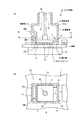
図6は、従来のこの種の電子部品のリペア装置の一例として、下記の特許文献1に記載
されたリペア電子部品の局部加熱装置を模式的に示した部分断面側面図である。
局部加熱装置51は、リペア電子部品であるBGAパッケージ52の上部に被せてプリ
ント配線基板53の平面部に密接させてシールドするシールドケース54と、シールドケ
ース54内部に配設され、熱風を噴き出すノズル部55を有する局部加熱ヒータ56と、
シールドケース54上部に配設され、シールドケース54をプリント配線基板53の平面
部に押圧して密接させるためのスプリング57及びスプリング支持板58とを含んで構成
されており、局部加熱ヒータ56のノズル部55から噴き出した熱風を、シールドケース
54内を循環させた後、シールドケース54の上部に設けられている排気穴59から上方
に排出させるようになっている。
FIG. 6 is a partial cross-sectional side view schematically showing a repair electronic component local heating device described in
The
A
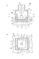
図7は、従来のこの種の電子部品のリペア装置の別の一例として、下記の特許文献2に
記載された電子部品交換用ノズル装置を模式的に示した部分断面側面図である。
電子部品交換用ノズル装置61は、交換対象のBGAパッケージ62を収容可能な空間
部64a、その開口端縁に排出口となる複数の切り欠き64b、及び回路基板63の部品
搭載面63aに着座させる着座部64cを有し、BGAパッケージ62と回路基板63と
の接合部を加熱・溶融するための熱風を供給する熱風供給用ノズル64と、熱風供給用ノ
ズル64の空間部64a内でBGAパッケージ62を吸着可能な部品吸着用ノズル65と
を備えている。熱風供給時には、回路基板63上における熱風供給用ノズル64内のBG
Aパッケージ62に対する熱風が切り欠き64bから熱風供給用ノズル64内に滞留する
ことなく排気されるようになっている。
FIG. 7 is a partial cross-sectional side view schematically showing an electronic component replacement nozzle device described in
The electronic component
The hot air for the
しかしながら、上記した特許文献1記載の装置では、局部加熱ヒータ56のノズル部5
5から噴き出された熱風は、方形状のBGAパッケージ52の四辺各方向からBGAパッ
ケージ52の下方に略同圧力で吹き込まれるようになっているので、BGAパッケージ5
2の底面に配列されているはんだバンプのうち、BGAパッケージ52中央付近のはんだ
バンプに対する熱風の吹き付け量が少なく、はんだバンプの温度が上昇しにくい構造とな
っていた。
However, in the apparatus described in
The hot air blown out from the BGA
Among the solder bumps arranged on the bottom surface of No. 2, the amount of hot air blown to the solder bump near the center of the BGA
また、上記した特許文献2記載の装置では、熱風供給用ノズル64に供給された熱風が
、BGAパッケージ62の四辺各側面に対向して位置する切り欠き64bから外部へ排出
されるようになっているので、BGAパッケージ62と回路基板63との間に熱風がほと
んど流れ込まず、すなわち、BGAパッケージ62の底面に配列されているはんだバンプ
に熱風が十分に吹き付けられず、特にパッケージ中央付近のはんだバンプの温度が上昇し
にくい構造となっていた。
Further, in the apparatus described in
このため、BGAパッケージ52、62の外縁付近と中心付近とのはんだバンプに温度
差が生じ、すなわち、BGAパッケージ52、62外縁近傍のはんだバンプは溶融してい
るが、BGAパッケージ52、62中央のはんだバンプは加熱不足により十分に溶融して
いない状態となり、この状態でBGAパッケージ52、62を基板から取り外そうとする
と、BGAパッケージ52、62の中央付近の基板上の配線等が損傷してしまい、その基
板が使用できなくなってしまう危険性があった。
Therefore, a temperature difference occurs between the solder bumps near the outer edge and the center of the
また、BGAパッケージ52、62の中心付近のはんだバンプを完全に溶かすためには
、熱風の温度を高めたり、風量を上げたり、熱風の供給時間を長くすればよいが、このよ
うな方法を採用するとBGAパッケージ52、62の周縁部や基板等に余分な熱が掛かり
、基板や部品を熱損傷させる危険性があった。また、このようなBGAパッケージ52、
62のはんだバンプ(接合部)における加熱温度分布が不均一となる問題は、パッケージ
サイズが大きくなるほど顕著に現れるという問題があった。
The problem that the heating temperature distribution in the 62 solder bumps (joint portions) becomes non-uniform is more noticeable as the package size increases.
本発明は上記課題に鑑みなされたものであって、電子部品取外しの際の基板と電子部品
との接合部における加熱温度を均一化することができ、基板や電子部品に損傷を与えるこ
となく電子部品の取り換えや修理等を行うことができるリペア用具、及び電子部品のリペ
ア装置を提供することを目的としている。
The present invention has been made in view of the above problems, and can uniformize the heating temperature at the joint between the substrate and the electronic component when the electronic component is removed, without causing damage to the substrate or the electronic component. An object of the present invention is to provide a repair tool capable of replacing or repairing parts, and a repair device for electronic parts.
上記目的を達成するために本発明に係るリペア用具(1)は、基板に搭載された電子部品に熱風を吹き付けるためのリペア用具であって、前記電子部品を収容するための開口部が底面に形成された筒状本体を備え、該筒状本体の前記開口部が、該開口部に前記電子部品を収容させた状態で、前記熱風を前記筒状本体の一側壁面内側からのみ前記電子部品の下方に流入させ、該電子部品と前記基板との間を経由させて、前記一側壁面に対向する第2の側壁面下から外部へ排出させるように構成され、前記筒状本体の第2の側壁面内側と該第2の側壁面に隣接する両側壁面内側とに、前記熱風がこれら側壁面側から前記電子部品の下方に流れ込まないようにするための熱風流入防止手段が配設され、該熱風流入防止手段が、少なくとも前記筒状本体の第2の側壁面内側と該第2の側壁面に隣接する両側壁面内側とを囲う形状をした板状体を備え、該板状体の下面に前記電子部品の上面周縁部を当接させ得るように構成されていることを特徴としている。 In order to achieve the above object, a repair tool (1) according to the present invention is a repair tool for blowing hot air onto an electronic component mounted on a board, and an opening for accommodating the electronic component is formed on the bottom surface. The electronic component is provided only from the inside of one side wall surface of the cylindrical main body with the cylindrical main body formed, and the opening of the cylindrical main body accommodates the electronic component in the opening. And is discharged from the second side wall surface opposite to the one side wall surface to the outside through the space between the electronic component and the substrate . The hot air inflow prevention means for preventing the hot air from flowing into the lower side of the electronic component from the side wall surface side is disposed on the side wall surface inner side and the both side wall inner surfaces adjacent to the second side wall surface, The hot air inflow prevention means is at least the cylindrical book A plate-like body having a shape surrounding the inner side of the second side wall surface and the inner sides of both side walls adjacent to the second side wall surface, and the upper peripheral edge of the electronic component is brought into contact with the lower surface of the plate-like body It is characterized by being configured to obtain .
上記リペア用具(1)によれば、前記筒状本体の前記開口部が、該開口部に前記電子部
品を収容させた状態で、前記熱風を前記筒状本体の一側壁面内側からのみ前記電子部品の
下方に流入させ、該電子部品と前記基板との間を経由させて、前記一側壁面に対向する第
2の側壁面下から外部へ排出させるように構成されているので、前記電子部品をリペアす
る際に、前記電子部品と前記基板との接合部に前記熱風を一定の方向で流し込むことがで
き、前記接合部の加熱を効率良く行うことができるとともに、前記接合部における加熱温
度を均一化することができ、前記接合部(例えば半田)の溶融状態のバラツキや、前記基
板や前記電子部品の局所的な過加熱等を防ぎ、前記基板や前記電子部品に損傷を与えるこ
となく前記電子部品のリペアを行うことができる。また前記熱風の温度を前記接合部の溶
融温度に近い温度に設定したり、前記接合部を溶融させるまでの時間を短縮させることも
可能となり、前記装置側の熱風を供給するための消費電力を低減させることができる。
According to the repair tool (1), in the state in which the opening portion of the cylindrical main body accommodates the electronic component in the opening portion, the hot air is transmitted only from the inside of one side wall surface of the cylindrical main body. The electronic component is configured to flow into the lower part of the component and pass through between the electronic component and the substrate to be discharged from below the second side wall surface facing the one side wall surface. In the repair, the hot air can be poured into the junction between the electronic component and the substrate in a certain direction, the heating of the junction can be performed efficiently, and the heating temperature at the junction can be increased. It is possible to make uniform, prevent variations in the molten state of the joint (for example, solder), local overheating of the substrate and the electronic component, and the like without damaging the substrate or the electronic component. Repair electronic parts Ukoto can. It is also possible to set the temperature of the hot air to a temperature close to the melting temperature of the joint, or to shorten the time until the joint is melted, and to reduce the power consumption for supplying hot air on the device side. Can be reduced.
上記リペア用具(1)によれば、前記熱風流入防止手段により、前記筒状本体の第2の
側壁面内側と該第2の側壁面に隣接する両側壁面内側とから前記熱風が前記電子部品の下
方に流れ込まない構造とすることができ、前記熱風を前記筒状本体の一側壁面内側からの
み前記電子部品の下方に流入させ、該電子部品と前記基板との間を経由させて、前記第2
の側壁面下から外部へ排出させることができる。
According to the repair tool ( 1 ), the hot air is prevented from flowing into the electronic component from the inner side of the second side wall surface of the cylindrical main body and the inner side surfaces of both sides adjacent to the second side wall surface by the hot air inflow prevention means. The hot air can flow into the lower part of the electronic component only from the inner side of the one side wall surface of the cylindrical main body, pass between the electronic component and the substrate, and 2
You can be discharged to the outside from the lower wall surface of the.
上記リペア用具(1)によれば、前記熱風流入防止手段が、少なくとも前記筒状本体の
第2の側壁面内側と該第2の側壁面に隣接する両側壁面内側とを囲う形状、例えば、平面
視略コの字形状、平面視略ロの字形状等をした板状体を備え、該板状体の下面に前記電子
部品の上面周縁部を当接させ得るように構成されているので、前記筒状本体の第2の側壁
面内側や該第2の側壁面に隣接する両側壁面内側に前記電子部品の側面を当接させなくて
も、前記板状体の下面に前記電子部品の上面周縁部を当接させることにより、前記筒状本
体の第2の側壁面内側と該第2の側壁面に隣接する両側壁面内側とから前記熱風が前記電
子部品の下方に流れ込まないようすることができる。また、前記板状体の内側方向への幅を利用することで、サイズの異なる前記電子部品のリペアにも使用することができ、また前記筒状本体を前記電子部品に被せる際の位置精度に余裕度を与えることができる。
According to the repair tool ( 1 ), the hot air inflow prevention means surrounds at least the second side wall surface inside the cylindrical main body and the both side wall inner surfaces adjacent to the second side wall surface, for example, a flat surface Since it is configured to have a plate-like body having a substantially U-shape in view, a substantially B-shape in plan view, and the like, the upper surface peripheral edge portion of the electronic component can be brought into contact with the lower surface of the plate-like body, Even if the side surface of the electronic component is not brought into contact with the inner side of the second side wall surface of the cylindrical main body or the side wall surfaces adjacent to the second side wall surface, the upper surface of the electronic component is placed on the lower surface of the plate-like body. By bringing the peripheral edge into contact with each other, the hot air may be prevented from flowing into the lower side of the electronic component from the inner side of the second side wall surface of the cylindrical main body and the inner side surfaces of both side walls adjacent to the second side wall surface. I can . In addition, by utilizing the width of the plate-like body in the inner direction, it can be used for repairing the electronic parts having different sizes, and the positional accuracy when the cylindrical body is put on the electronic parts is improved. A margin can be given.
また本発明に係るリペア用具(2)は、上記リペア用具(1)において、前記板状体が
、前記筒状本体の第2の側壁面内側と該第2の側壁面に隣接する両側壁面内側とに沿って
上下方向に移動可能に構成されていることを特徴としている。
Further, the repair tool ( 2 ) according to the present invention is the repair tool ( 1 ), wherein the plate-like body is located on the inner side of the second side wall surface of the tubular body and on the inner side of both side walls adjacent to the second side wall surface. It is characterized by being configured to be movable in the vertical direction along the lines.
上記リペア用具(2)によれば、前記板状体が、前記筒状本体の第2の側壁面内側と該
第2の側壁面に隣接する両側壁面内側とに沿って上下方向に移動可能に構成されているの
で、前記板状体の下面に前記電子部品の上面周縁部を当接させた状態で、前記電子部品を
上下方向に移動させることができる。したがって、高さの異なる前記電子部品であっても
、前記筒状本体の第2の側壁面内側と該第2の側壁面に隣接する両側壁面内側とから前記
熱風が前記電子部品の下方に流れ込まないようすることができる。また、前記電子部品の
取り外し等の作業も問題なく行うことができる。
According to the repair tool ( 2 ), the plate-like body is movable in the vertical direction along the second side wall surface inside of the cylindrical main body and the both side wall surfaces adjacent to the second side wall surface. Since it is comprised, the said electronic component can be moved to an up-down direction in the state which contacted the upper surface peripheral part of the said electronic component with the lower surface of the said plate-shaped object. Therefore, even in the electronic component having a different height, the hot air flows into the lower part of the electronic component from the inside of the second side wall surface of the cylindrical main body and the inside of both side wall surfaces adjacent to the second side wall surface. Can not be. In addition, operations such as removal of the electronic component can be performed without any problem.
また本発明に係るリペア用具(3)は、上記リペア用具(1)又は(2)において、前記筒状本体の第2の側壁面下から排出される熱風の排出方向を変える排出方向変更手段を備えていることを特徴としている。 Further, the repair tool ( 3 ) according to the present invention includes a discharge direction changing means for changing a discharge direction of hot air discharged from below the second side wall surface of the cylindrical body in the repair tool (1) or (2) . It is characterized by having.
上記リペア用具(3)によれば、前記排出方向変更手段により、前記筒状本体の第2の
側壁面下から排出される熱風の排出方向を変えることができ、前記基板上に搭載されてい
る他の部品に熱風が吹き付けられないようにすることができ、前記他の部品の熱損傷を回
避することができる。
According to the repair tool ( 3 ), the discharge direction changing means can change the discharge direction of hot air discharged from below the second side wall surface of the cylindrical main body, and is mounted on the substrate. It is possible to prevent hot air from being blown to other parts, and to avoid thermal damage of the other parts.
また本発明に係るリペア用具(4)は、基板に搭載された電子部品に熱風を吹き付けるためのリペア用具であって、前記電子部品を収容するための開口部が底面に形成された筒状本体を備え、該筒状本体の開口部が、該開口部に前記電子部品を収容させた状態で、前記熱風を前記筒状本体の一側壁面を除く複数の側壁面内側から前記電子部品の下方に流入させ、該電子部品と前記基板との間を経由させて、前記一側壁面下から外部へ排出させるように構成され、前記筒状本体の一側壁面内側に、前記熱風が前記一側壁面側から前記電子部品の下方に流れ込まないようするための熱風流入防止手段が配設され、該熱風流入防止手段が、少なくとも前記筒状本体の一側壁面内側を囲う形状をした板状体を備え、該板状体の下面に前記電子部品の上面周縁部を当接させ得るように構成されていることを特徴としている。 Moreover, the repair tool ( 4 ) according to the present invention is a repair tool for blowing hot air onto an electronic component mounted on a substrate, and a cylindrical main body having an opening for accommodating the electronic component formed on the bottom surface In the state where the opening of the cylindrical main body accommodates the electronic component in the opening, the hot air is sent from the inside of a plurality of side wall surfaces excluding one side wall surface of the cylindrical main body to the lower side of the electronic component. The hot air flows into the one side wall surface of the cylindrical main body through the space between the electronic component and the substrate. A hot air inflow prevention means for preventing the air from flowing from the wall surface to the lower side of the electronic component is disposed, and the hot air inflow prevention means includes a plate-like body having a shape surrounding at least one side wall surface of the cylindrical body. Comprising the electronic component on the lower surface of the plate-like body. It is characterized by being configured so as to contact the surface periphery.
上記リペア用具(4)によれば、前記筒状本体の開口部が、該開口部に前記電子部品を
収容させた状態で、前記熱風を前記筒状本体の一側壁面を除く複数の側壁面内側から前記
電子部品の下方に流入させ、該電子部品と前記基板との間を経由させて、前記一側壁面下
から外部へ排出させるように構成されているので、前記電子部品をリペアする際に、前記
電子部品と前記基板との接合部に前記熱風を前記複数の側壁面内側から一定の方向に流し
込むことができ、前記接合部の加熱を一層効率良く行うことができるとともに、前記接合
部における加熱温度を均一化することができ、前記接合部の溶融状態のバラツキや、前記
基板や電子部品の局所的な過加熱等を防ぎ、前記基板や前記電子部品に損傷を与えること
なく前記電子部品のリペアを行うことができる。また前記熱風の温度を前記接合部の溶融
温度に近い温度に設定したり、前記接合部を溶融させるまでの時間を短縮させることも可
能となり、前記装置側の加熱ヒータ等の消費電力を低減させることができる。
According to the repair tool ( 4 ), a plurality of side wall surfaces excluding one side wall surface of the cylindrical main body in a state where the opening of the cylindrical main body accommodates the electronic component in the opening. When the electronic component is repaired, it flows into the lower part of the electronic component from the inside, passes through between the electronic component and the substrate, and is discharged from the bottom of the one side wall surface to the outside. In addition, the hot air can be poured into the bonding portion between the electronic component and the substrate in a certain direction from the inside of the plurality of side wall surfaces, and the bonding portion can be heated more efficiently. The heating temperature can be made uniform, and it is possible to prevent variations in the molten state of the joints, local overheating of the substrate and electronic components, and the like without damaging the substrate or electronic components. Repair parts Ukoto can. It is also possible to set the temperature of the hot air to a temperature close to the melting temperature of the joint, and to shorten the time until the joint is melted, thereby reducing the power consumption of the heater on the apparatus side. be able to.
上記リペア用具(4)によれば、前記熱風流入防止手段により、前記筒状本体の一側壁
面内側から前記熱風が前記電子部品の下方に流れ込まない構造とすることができ、前記熱
風を前記筒状本体の前記複数の側壁面内側から前記電子部品の下方に流入させ、該電子部
品と前記基板との間を経由させて、前記一側壁面下から外部へ排出させることができる。
According to the repair tool ( 4 ), the hot air inflow prevention means can be configured to prevent the hot air from flowing from the inside of one side wall surface of the cylindrical main body to the lower side of the electronic component. It can flow into the lower part of the electronic component from the inside of the plurality of side wall surfaces of the main body, and can be discharged to the outside through the space between the electronic component and the substrate.
上記リペア用具(4)によれば、前記熱風流入防止手段が、少なくとも前記筒状本体の一側壁面内側を囲う形状をした板状体を備え、該板状体の下面に前記電子部品の上面周縁部を当接させ得るように構成されているので、前記筒状本体の一側壁面に前記電子部品の側面を当接させなくても、前記板状体の下面に前記電子部品の上面周縁部を当接させることにより、前記筒状本体の一側壁面内側から前記熱風が前記電子部品の下方に流れ込まないようすることができる。また、前記板状体の内側方向への幅を利用することで、サイズの異なる前記電子部品のリペアにも使用することができ、また前記筒状本体を前記電子部品に被せる際の位置精度に余裕度を与えることができる。 According to the repair tool ( 4 ), the hot air inflow prevention means includes a plate-like body having a shape surrounding at least one side wall surface of the cylindrical main body, and the upper surface of the electronic component is provided on the lower surface of the plate-like body. Since the peripheral portion can be brought into contact, the upper peripheral edge of the electronic component can be brought into contact with the lower surface of the plate-like body without contacting the side surface of the electronic component with one side wall surface of the cylindrical body. By abutting the part, the hot air can be prevented from flowing into the lower side of the electronic component from the inside of one side wall surface of the cylindrical main body. In addition, by utilizing the width of the plate-like body in the inner direction, it can be used for repairing the electronic parts having different sizes, and the positional accuracy when the cylindrical body is put on the electronic parts is improved. A margin can be given.
また本発明に係るリペア用具(5)は、上記リペア用具(4)において、前記板状体が、前記筒状本体の一側壁面内側に沿って上下方向に移動可能に構成されていることを特徴としている。 Moreover, the repair tool ( 5 ) which concerns on this invention WHEREIN: In the said repair tool ( 4 ), the said plate-shaped body is comprised so that a vertical movement is possible along the one side wall surface inside of the said cylindrical main body. It is a feature.
上記リペア用具(5)によれば、前記板状体が、前記筒状本体の一側壁面内側に沿って上下方向に移動可能に構成されているので、前記板状体の下面に前記電子部品の上面周縁部を当接させた状態で、前記電子部品を上下方向に移動させることができる。したがって、高さの異なる前記電子部品であっても、前記筒状本体の一側壁面内側から前記熱風が前記電子部品の下方に流れ込まないようすることができる。また、前記電子部品の取り外し等の作業も問題なく行うことができる。 According to the repair tool ( 5 ), since the plate-like body is configured to be movable in the vertical direction along the inner side wall surface of the cylindrical body, the electronic component is placed on the lower surface of the plate-like body. The electronic component can be moved in the up-down direction in a state in which the peripheral edge of the upper surface is in contact. Therefore, even if the electronic components have different heights, the hot air can be prevented from flowing into the lower side of the electronic component from the inside of one side wall surface of the cylindrical main body. In addition, operations such as removal of the electronic component can be performed without any problem.
また本発明に係るリペア用具(6)は、上記リペア用具(4)又は(5)において、前記筒状本体の一側壁面下から排出される熱風の排出方向を変える排出方向変更手段を備えていることを特徴としている。 Moreover, the repair tool ( 6 ) which concerns on this invention is equipped with the discharge direction change means which changes the discharge direction of the hot air discharged from the one side wall surface of the said cylindrical main body in the said repair tool (4) or (5) . It is characterized by being.
上記リペア用具(6)によれば、前記排出方向変更手段により、前記筒状本体の一側壁面下から排出される熱風の排出方向を変えることができ、前記基板上に搭載されている他の部品に熱風が吹き付けられないようにすることができ、前記他の部品の熱損傷を回避することができる。 According to the repair tool ( 6 ), the discharge direction changing means can change the discharge direction of the hot air discharged from the one side wall surface of the cylindrical main body, and the other mounted on the substrate. It is possible to prevent hot air from being blown to the parts, and to avoid thermal damage of the other parts.
また本発明に係るリペア用具(7)は、上記リペア用具(1)〜(6)のいずれかにおいて、前記筒状本体が、断熱部材を含んで構成されていることを特徴としている。
上記リペア用具(7)によれば、前記筒状本体が、断熱部材を含んで構成されているので、前記筒状本体の内部の熱が外部に放熱されにくい構造とすることができ、前記筒状本体内部での前記熱風による加熱効率を一層高めることができる。
Moreover, the repair tool ( 7 ) which concerns on this invention is characterized by the said cylindrical main body being comprised including the heat insulation member in any one of the said repair tools (1)-( 6 ).
According to the repair tool ( 7 ), since the cylindrical main body includes a heat insulating member, the heat inside the cylindrical main body can be made difficult to be radiated to the outside. The heating efficiency by the hot air inside the main body can be further increased.
また本発明に係る電子部品のリペア装置(1)は、上記リペア用具(1)〜(7)のいずれかが装着されることを特徴としている。
上記電子部品のリペア装置(1)によれば、上記リペア用具(1)〜(7)の各効果を得ることができるリペア装置を実現することができる。
An electronic component repair device (1) according to the present invention is characterized in that any one of the repair tools (1) to ( 7 ) is mounted.
According to the electronic device repair device (1), it is possible to realize a repair device capable of obtaining the effects of the repair tools (1) to ( 7 ).
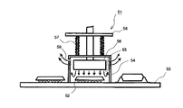
以下、本発明に係るリペア用具、及びリペア装置の実施の形態を図面に基づいて説明す
る。図1(a)は、実施の形態(1)に係るリペア用具を用いて電子部品(この場合、B
GAパッケージ)のリペアを行っている状態を模式的に示した部分側面断面図であり、図
1(b)は、図1(a)におけるB−B線断面図である。また図2は、実施の形態(1)
に係るリペア用具を模式的に示した斜視図である。
DESCRIPTION OF EMBODIMENTS Hereinafter, embodiments of a repair tool and a repair device according to the present invention will be described with reference to the drawings. FIG. 1A shows an electronic component (in this case, B) using the repair tool according to the embodiment (1).
FIG. 1B is a partial cross-sectional side view schematically showing a state in which the GA package is being repaired, and FIG. 1B is a cross-sectional view taken along line BB in FIG. FIG. 2 shows the embodiment (1).
It is the perspective view which showed typically the repair tool which concerns on.
図中10は、プリント配線基板(以下、単に基板と記す)1上に搭載されたBGAパッ
ケージ2をリペアする装置(図示せず)に装着され、BGAパッケージ2に熱風を吹き付
けるためのリペア用具を示している。
In the figure,
リペア用具10は、BGAパッケージ2を収容するための略矩形形状の開口部12が底
面に形成された筒状本体11から構成されている。筒状本体11は、断熱材(例えば、セ
ラミックファイバー等)を用いて形成されており、筒状本体11の側壁面13は、側壁面
13の略中央付近から内側に向けて所定幅ほど折り曲げられた後、対向する側壁面14と
略平行となるように折り返された形状となっている。
The
側壁面13の下端部13aは他の側壁面14、15、16の各下端部より上方に位置し
、筒状本体11の開口部12を基板1上のBGAパッケージ2に被せたときに、基板1と
側壁面13の下端部13aとの間に、熱風を排出するための隙間Aが形成されるようにな
っている。隙間Aの高さは、リペアするBGAパッケージ2の側面が側壁面13の下端部
13a内側に当接可能な高さ、かつ熱風が円滑に排出可能な高さに設定されている。
When the
筒状本体11の側壁面13の下端部13a内側から側壁面14内側までの幅Bは、BG
Aパッケージ2の横幅よりも大きくなるように、すなわち、側壁面13の下端部13a内
側にBGAパッケージ2の側面を当接させた状態で、側壁面14内側とBGAパッケージ
2の側面とに、熱風流入部となる所定幅の隙間Dが形成されるように設定されている。一
方、筒状本体11の側壁面15内側から側壁面16内側までの幅Cは、BGAパッケージ
2の縦幅と略同一に設定されており、筒状本体11の側壁面15、16の各内側にBGA
パッケージ2の側面が当接可能な(すなわち、熱風が流れ込まない)形状になっている。
The width B from the inside of the
Hot air is applied to the inside of the
The side surface of the
また、筒状本体11の側壁面13の下端部13aの外側には、側壁面15、16に接合
された熱風流路変更板17が配設され、側壁面13の下端部13aと熱風流路変更板17
とにより、熱風の排気流路18aと排気口18bとが形成されている。
A hot air flow
Thus, a hot
また、筒状本体11の上方には熱風を噴き出す加熱ヒータ(図示せず)が配設されてお
り、加熱ヒータからの熱風が、筒状本体11の内部空間11aに供給されるようになって
いる。また、内部空間11aには、BGAパッケージ2を吸着するための部品吸着用ノズ
ル30が昇降可能に配設されている。リペア用具10は、不図示のリペア装置によって、
上下方向への移動、及び所定の水平方向への移動などの駆動制御が行われるようになって
いる。また、基板1の下面側には、ボトムヒータ31が配設されており、加熱ヒータやボ
トムヒータ31の加熱制御もリペア装置により行われるようになっている。
Further, a heater (not shown) for blowing hot air is disposed above the cylindrical
Drive control such as movement in the vertical direction and movement in a predetermined horizontal direction is performed. Further, a
次に、実施の形態(1)に係るリペア用具10を用いたBGAパッケージ2のリペア方
法について、図1を用いて説明する。機能検査等で不良品と判断されたBGAパッケージ
2を良品のBGAパッケージ2と交換するには、従来と同様、基板1上の不良品のBGA
パッケージ2を取り外した後、基板1上に良品のBGAパッケージ2を取り付けることに
より行う。
Next, a repair method for the
After the
まず、基板1上から不良品のBGAパッケージ2を取り外す場合、基板1をリペア装置
のX−Yテーブル(図示せず)に固定し、不良品のBGAパッケージ2をリペア用具10
下方の決めされた所定位置に配置する。
First, when the
It is arranged at a predetermined position below.
次に、BGAパッケージ2の上方からリペア用具10を下降させて、筒状本体11の開
口部12をBGAパッケージ2に被せて、筒状本体11の側壁面14、15、16、及び
熱風流路変更板17の下端部を基板1上に当接(着座)させる。このとき側壁面13の下
端部13a内側と、側壁面15、16の各内側とにBGAパッケージ2の側面を当接させ
るようにリペア用具10が駆動制御される。
Next, the
次に、加熱ヒータを作動させて、所定温度に設定された熱風をリペア用具10の筒状本
体11の上部からBGAパッケージ2に向けて供給するとともに、ボトムヒータ31によ
り基板1下側からも加熱を行う。このとき、筒状本体11の上部からBGAパッケージ2
に向けて供給される熱風は、筒状本体11の側壁面14内側とBGAパッケージ2との隙
間DからのみBGAパッケージ2の下方に流れ込み、流れ込んだ熱風は、基板1とBGA
パッケージ2との接合部2aを経由して、側壁面13の下端部13a下の隙間Aから排気
流路18aを通って、排気口18bから外部へ排出されるようになっており、熱風により
BGAパッケージ2の接合部2aが短時間で均一に加熱・溶融されるようになっている。
Next, the heater is operated to supply hot air set to a predetermined temperature from the upper part of the cylindrical
The hot air supplied toward the air flows into the lower side of the
Via the joint 2a with the
その後、BGAパッケージ2の接合部2aを溶融させるのに必要な所定時間ほど熱風を
供給した後、部品吸着用ノズル30でBGAパッケージ2を吸着して上昇させることによ
り、BGAパッケージ2を基板1から取り外すとともに、リペア用具10も上昇させて、
所定の位置に退避させる。
Thereafter, hot air is supplied for a predetermined time required to melt the
Retreat to a predetermined position.
次に、基板1上に良品のBGAパッケージ2を取り付ける際は、これと反対の動作で行
われる。まず、良品のBGAパッケージ2を部品吸着用ノズル30で吸着し、BGAパッ
ケージ2が筒状本体11の内部に保持された状態のリペア用具10を基板1の所定の取り
付け位置に下降させて、BGAパッケージ2を基板1の所定の取り付け位置に載置する。
このとき筒状本体11の開口部12を形成する側壁面14、15、16、及び熱風流路変
更板17の下端部は基板1上に当接され、側壁面13の下端部13a内側と、側壁面15
、16の各内側とにBGAパッケージ2の側面を当接させるようにリペア用具10の駆動
制御が行われる。
Next, when the
At this time, the
Drive control of the
次に、加熱ヒータを作動させて、所定温度に設定された熱風をリペア用具10の筒状本
体11の上方からBGAパッケージ2に向けて供給するとともに、ボトムヒータ31によ
り基板1の下側からも加熱を行う。
Next, the heater is operated to supply hot air set to a predetermined temperature from above the cylindrical
このとき、筒状本体11の上部からBGAパッケージ2に向けて供給された熱風は、筒
状本体11の側壁面14内側とBGAパッケージ2との隙間DからのみBGAパッケージ
2の下方に流れ込み、流れ込んだ熱風は、基板1とBGAパッケージ2との接合部2aを
経由して、側壁面13の下端部13a下の隙間Aから排気流路18aを通って、排気口1
8bから外部へ排出されるようになっており、熱風によりBGAパッケージ2の接合部2
aが短時間で均一に加熱・溶融される。所定時間加熱して、BGAパッケージ2の接合部
2aと基板1の接点とを接合させた後、部品吸着用ノズル30の吸引を解除して、リペア
用具10を上方に退避させて、BGAパッケージ2の取り付けを終える。
At this time, the hot air supplied from the upper part of the cylindrical
8b is discharged to the outside, and hot air blows the
a is uniformly heated and melted in a short time. After heating for a predetermined time to join the joint 2a of the
上記実施の形態(1)に係るリペア用具10によれば、筒状本体11の開口部12が、
リペアするBGAパッケージ2のサイズを考慮して、筒状本体11の側壁面13の下端部
13a内側と、側壁面15、16の各内側とに、BGAパッケージ2の側面を当接可能な
形状になっているので、筒状本体11の側壁面13の下端部13a内側と側壁面15、1
6の各内側とにBGAパッケージ2の側面を当接させた状態(すなわち、熱風が流れ込ま
ない状態)で、BGAパッケージ2を開口部12に収容させることができ、熱風を筒状本
体11の側壁面14内側の隙間DからのみBGAパッケージ2の下方に流入させ、BGA
パッケージ2と基板1との接合部2aを経由させて、側壁面13の下端部13a下の隙間
Aから排気流路18aを通って、排気口18bから外部へ排出させることができる。した
がって、BGAパッケージ2の接合部2aに熱風を一定の方向で流し込むことができ、B
GAパッケージ2の接合部2aの加熱を熱風により効率良く行うことができるとともに、
接合部2aにおける加熱温度を均一化することができ、接合部2a(半田)の溶融状態の
バラツキや、基板1やBGAパッケージ2の局所的な過加熱等を防ぎ、基板1やBGAパ
ッケージ2に損傷を与えることなくBGAパッケージ2のリペアを行うことができる。ま
た熱風の温度を接合部2aの溶融温度に近い温度に設定したり、接合部2aを溶融させる
までの時間を短縮させることも可能となり、リペア装置側の熱風を供給するための加熱ヒ
ータ等の消費電力を低減させることができる。
According to the
Considering the size of the
6, the
Via the joint 2a between the
While heating the
The heating temperature at the
また、熱風流路変更板(排出方向変更手段)17により、筒状本体11の側壁面13の
下端部13a下の隙間Aから排出される熱風の排出方向を上向きに変えることができ、基
板1上に搭載されている他の部品に熱風が吹き付けられない構造にすることができ、基板
1上の他の部品の熱損傷を回避することができる。
Further, the hot air flow path changing plate (discharge direction changing means) 17 can change the discharge direction of the hot air discharged from the gap A below the
また、筒状本体11が、断熱部材から構成されているので、筒状本体11の内部の熱が
外部に放熱されにくい構造にすることができ、筒状本体11内部での熱風による加熱効率
を一層高めることができる。
Moreover, since the cylindrical
図3(a)は、実施の形態(2)に係るリペア用具を用いてBGAパッケージのリペア
を行っている状態を模式的に示した部分側面断面図であり、図3(b)は、図3(a)に
おけるB−B線断面図である。但し、図1に示したリペア用具10と同一機能を有する構
成部品には同一符号を付し、ここではその説明を省略する。
FIG. 3A is a partial side cross-sectional view schematically showing a state in which the BGA package is repaired using the repair tool according to the embodiment (2), and FIG. It is a BB line sectional view in 3 (a). However, the same reference numerals are given to components having the same functions as those of the
実施の形態(1)に係るリペア用具10では、筒状本体11の開口部12が、リペアす
るBGAパッケージ2のサイズを考慮して、筒状本体11の側壁面13の下端部13a内
側と側壁面15、16の各内側とに、BGAパッケージ2の側面を当接可能な形状になっ
ているが、実施の形態(2)に係るリペア用具10Aでは、筒状本体11Aの内部空間1
1aに、筒状本体11Aの側壁面13内側と、側壁面15、16の各内側とに接した状態
で、上下方向に移動可能な平面視略コの字形状をした断面L字型の熱風流入防止板20が
配設されている点が、実施の形態(1)に係るリペア用具10との主な相違点である。
In the
1a, hot air having an L-shaped cross section having a substantially U-shape in plan view that is movable in the vertical direction while being in contact with the inside of the
実施の形態(2)に係るリペア用具10Aでは、熱風流入防止板20の下面にBGAパ
ッケージ2の上面周縁部を当接させた状態で、熱風供給等のリペア操作が行われるように
なっている。熱風流入防止板20の下面の内側方向への張り出し幅Eは、リペアするBG
Aパッケージ2のサイズを考慮して必要な幅に設定されている。
In the
The required width is set in consideration of the size of the
また、筒状本体11Aの側壁面13の下端部13a内側から側壁面14内側までの幅B
は、BGAパッケージ2の横幅よりも大きくなるように、すなわち、側壁面13内側の熱
風流入防止板20の下面にBGAパッケージ2の上面周縁部を当接させた状態で、側壁面
14内側とBGAパッケージ2の側面との間に、熱風流入部となる所定幅の隙間Dが形成
されるように設定されている。一方、筒状本体11Aの側壁面15内側から側壁面16内
側までの幅Cは、BGAパッケージ2の縦幅よりもやや大きく設定されており、筒状本体
11Aの側壁面15、16の各内側に配設された熱風流入防止板20の下面にBGAパッ
ケージ2の上面周縁部が当接されるようになっている。
Further, the width B from the inside of the
Is larger than the width of the
また、筒状本体11Aの側壁面13の下端部13a内側と、側壁面15、16の各内側
とには、熱風流入防止板20の下面側を係止するための突起状の係止片21が形成され、
側壁面15、16の各内側とには、熱風流入防止板20の横ずれを防止するための突起状
のずれ防止片22が形成されている。
Further, a protruding
On each inner side of the side wall surfaces 15, 16, a protruding
実施の形態(2)に係るリペア用具10Aを用いたBGAパッケージ2のリペア方法に
ついては、上記した実施の形態(1)に係るリペア用具10を用いた場合と略同様な方法
で行なわれるようになっており、図3に示しているように、筒状本体11Aの上部からB
GAパッケージ2に向けて供給された熱風は、筒状本体11Aの側壁面14内側とBGA
パッケージ2の側面との隙間DからのみBGAパッケージ2の下方に流れ込み、流れ込ん
だ熱風は、基板1とBGAパッケージ2との接合部2aを経由して、側壁面13の下端部
13a下の隙間Aから排気流路18aを通って、排気口18bから外部へ排出されるよう
になっている。
The repair method for the
The hot air supplied toward the
The hot air that has flowed into the lower part of the
上記実施の形態(2)に係るリペア用具10Aによれば、筒状本体11の側壁面13内
側と側壁面15、16の各内側とを囲う平面視略コの字形状をした断面L字形の熱風流入
防止板20が、その下面にBGAパッケージ2の上面周縁部を当接させ得るように配設さ
れているので、筒状本体11Aの側壁面13内側と側壁面15、16の各内側とから熱風
がBGAパッケージ2の下方に流れ込まない構造とすることができ、熱風を筒状本体11
Aの側壁面14内側からのみBGAパッケージ2の下方に流入させ、BGAパッケージ2
と基板1との間の接合部2aを経由させて、側壁面13の下端部13a下の隙間Aから排
気流路18aを通って、排気口18bから外部へ排出させることができ、上記実施の形態
(1)に係るリペア用具10と略同様の効果を得ることができる。
According to the
The
Through the joint 2a between the
また、熱風流入防止板20の内側方向への幅を利用することで、サイズの異なるBGA
パッケージ2のリペアにも使用することができ、また筒状本体11AをBGAパッケージ
2に被せる際の位置精度に余裕度を与えることができる。
In addition, by using the width of the hot air
It can also be used for repairing the
また、熱風流入防止板20が、筒状本体11Aの側壁面13内側と側壁面15、16の
各内側とに沿って上下方向に移動するように構成されているので、筒状本体11Aの内部
でBGAパッケージ2を上下方向に移動させることができ、部品吸着用ノズル30による
BGAパッケージ2の取り外し等の作業を支障なく行うことができ、また、筒状本体11
AをBGAパッケージ2に被せた際に、熱風流入防止板20の下面とBGAパッケージ2
の上面周縁部とを当接させた状態で、熱風流入防止板20を上方向に移動させることがで
きるので、高さの異なるBGAパッケージ2に対しても適用することができる。
Moreover, since the hot air
When A is put on the
Since the hot air
なお、上記実施の形態(2)に係るリペア用具10Aでは、熱風流入防止板20が、側
壁面13の下端部13a、側壁面15、16の内側に沿って上下方向に移動できるように
なっているが、別の実施の形態では、リペアするBGAパッケージ2の高さ位置を考慮し
て、熱風流入防止板20を側壁面13、15、16内側に固定した構造としてもよく、こ
の場合、BGAパッケージ2を取り外す際に、部品吸着用ノズル30でBGAパッケージ
2を吸着した状態で、リペア用具10Aを上昇させるようにすれば、取り外し等も支障な
く行うことができる。
In the
また、熱風流入防止板20を係止させる係止片21やずれ防止片22を設ける代わりに
、熱風流入防止板20と部品吸着用ノズル30とを連結棒等の連結部材により連結させて
、部品吸着用ノズル30の昇降動作に連動させて熱風流入防止板20を昇降させる構造と
してもよく、この場合、部品吸着用ノズル30でBGAパッケージ2を吸着した状態で、
熱風流入防止板20の下面にBGAパッケージ2の上面周縁部を当接させるようにすれば
、熱風が側壁面13の下端部13a、側壁面15、16の各内側から下方に流れ込むこと
なく、リペア作業を支障なく行うことができる。
Further, instead of providing the
If the upper peripheral edge of the
また、実施の形態(2)では、熱風流入防止板20として、平面視略コの字形状をした
ものを適用したが、熱風流入防止板20の形状は、少なくとも筒状本体11Aの側壁面1
3内側と側壁面15、16内側とを囲う形状のものであればよく、例えば平面視略ロの字
形状(BGAパッケージ2の上面周縁部を囲う形状)をしたものなども適用することがで
きる。
In the embodiment (2), the hot air
3 may be of any shape that surrounds the inner side and the inner side of the side wall surfaces 15, 16. For example, a shape having a substantially square shape in a plan view (a shape that surrounds the peripheral edge of the upper surface of the BGA package 2) can also be applied. .
図4(a)は、実施の形態(3)に係るリペア用具を用いてBGAパッケージのリペア
を行っている状態を模式的に示した部分側面断面図であり、図4(b)は、図4(a)に
おけるB−B線断面図である。但し、図1に示したリペア用具10と同一機能を有する構
成部品には同一符号を付し、ここではその説明を省略する。
FIG. 4A is a partial side cross-sectional view schematically showing a state in which the BGA package is repaired using the repair tool according to the embodiment (3), and FIG. It is a BB line sectional view in 4 (a). However, the same reference numerals are given to components having the same functions as those of the
実施の形態(1)に係るリペア用具10では、筒状本体11の開口部12が、リペアす
るBGAパッケージ2のサイズを考慮して、筒状本体11の側壁面13の下端部13a内
側と側壁面15、16の各内側とに、BGAパッケージ2の側面を当接可能な形状になっ
ているが、実施の形態(3)に係るリペア用具10Bでは、筒状本体11Bの開口部12
が、リペアするBGAパッケージ2のサイズを考慮して、筒状本体11の側壁面13の下
端部13a内側にのみBGAパッケージ2の側面を当接可能な形状になっている。
In the
However, in consideration of the size of the
すなわち、筒状本体11Bの開口部12が、開口部12にBGAパッケージ2を収容さ
せた状態で、熱風を筒状本体11Bの側壁面13を除く側壁面14、15、16の内側か
らBGAパッケージ2の下方に流入させ、該流入させた熱風を、基板1とBGAパッケー
ジ2との接合部2aを経由させて、側壁面13の下端部13aに形成された矩形形状の切
り欠き部13bから排気流路18aを通して、排気口18bから排出させるように形成さ
れている。なお、切り欠き部13bの高さは、リペアするBGAパッケージ2の高さより
も低く、その幅は、熱風が円滑に排出可能なサイズに設定されている。
That is, in the state where the
筒状本体11Bの側壁面13の下端部13a内側から側壁面14内側までの幅Bは、B
GAパッケージ2の横幅よりも大きくなるように、すなわち、側壁面13の下端部13a
内側にBGAパッケージ2の側面を当接させた状態で、側壁面14内側とBGAパッケー
ジ2の側面との間に、熱風流入部となる所定幅の隙間Dが形成されるように設定されてい
る。一方、筒状本体11Bの側壁面15内側から側壁面16内側までの幅Cは、BGAパ
ッケージ2の縦幅よりも大きく設定されており、筒状本体11の側壁面15、16の各内
側とBGAパッケージ2の両側面との間に、熱風流入部となる所定幅の隙間Fが形成され
るようになっている。
The width B from the inside of the
The
A gap D having a predetermined width as a hot air inflow portion is formed between the inside of the
実施の形態(3)に係るリペア用具10Bを用いたBGAパッケージ2のリペア方法に
ついては、上記した実施の形態(1)に係るリペア用具10を使用した場合と略同様な方
法で行なわれるようになっており、図4に示しているように、筒状本体11Bの上部から
BGAパッケージ2に向けて供給された熱風は、筒状本体11Bの側壁面14、15、1
6の各内側とBGAパッケージ2の側面との隙間D、FからBGAパッケージ2の下方に
流れ込み、流れ込んだ熱風は、基板1とBGAパッケージ2との接合部2aを経由して、
側壁面13の下端部13aに形成された切り欠き部13bから排気流路18aを通って、
排気口18bから外部へ排出されるようになっている。
About the repair method of the
6 and the gap D, F between the inner side of the
From the
It is discharged from the
上記実施の形態(3)に係るリペア用具10Bによれば、筒状本体11Bの開口部12
が、リペアするBGAパッケージ2のサイズを考慮して、筒状本体11Bの側壁面13の
下端部13a内側にのみBGAパッケージ2の側面を当接可能な形状になっているので、
筒状本体11Bの側壁面13の下端部13a内側にBGAパッケージ2の一側面を当接さ
せた状態(すなわち、熱風が流れ込まない状態)で、BGAパッケージ2を開口部12に
収容させることにより、熱風を筒状本体11Bの側壁面14、15、16の各内側の隙間
D、FからBGAパッケージ2の下方に流入させ、BGAパッケージ2と基板1との接合
部2aを経由させて、側壁面13の下端部13aに形成された切り欠き部13bから排気
流路18aを通って、排気口18bから外部へ排出させることができる。したがって、B
GAパッケージ2の接合部2aに熱風を複数の側壁面内側から一定の方向に流し込むこと
ができ、BGAパッケージ2の接合部2aの加熱を一層効率良く行うことができ、上記実
施の形態(1)に係るリペア用具10と略同様な効果を得ることができる。
According to the
However, in consideration of the size of the
By accommodating the
Hot air can be poured into the
図5(a)は、実施の形態(4)に係るリペア用具を用いてBGAパッケージのリペア
を行っている状態を模式的に示した部分側面断面図であり、図5(b)は、図5(a)に
おけるB−B線断面図である。但し、図4に示したリペア用具10Bと同一機能を有する
構成部品には同一符号を付し、ここではその説明を省略する。
FIG. 5A is a partial side cross-sectional view schematically showing a state in which the BGA package is repaired using the repair tool according to the embodiment (4), and FIG. It is a BB line sectional view in 5 (a). However, the same reference numerals are given to components having the same functions as those of the
実施の形態(4)に係るリペア用具10Cでは、筒状本体11Cの側壁面13内側に、
熱風がBGAパッケージ2の下方に流れ込まないようするために、筒状本体11Cの側壁
面13内側に当接させた状態で上下に移動可能な断面L字型の熱風流入防止板20Aが配
設されている点が、実施の形態(3)に係るリペア用具10Bと相違している。
In the
In order to prevent hot air from flowing below the
実施の形態(4)に係るリペア用具10Cでは、熱風流入防止板20Aの下面にBGA
パッケージ2の上面周縁部を当接させた状態で、熱風供給等のリペア操作が行われるよう
になっている。熱風流入防止板20Aの下面の内側への張り出し幅Eは、リペアするBG
Aパッケージ2のサイズを考慮して必要な幅に設定されている。
In the
A repair operation such as supplying hot air is performed in a state in which the peripheral edge of the upper surface of the
The required width is set in consideration of the size of the
また、筒状本体11Cの側壁面13の下端部13a内側と、側壁面15、16の各内側
とには、熱風流入防止板20Aの下面側を係止するための突起状の係止片21が形成され
、側壁面15、16の各内側とには、熱風流入防止板20Aの横ずれを防止するための突
起状のずれ防止片22が形成されている。
Further, a protruding
実施の形態(4)に係るリペア用具10Cを用いたBGAパッケージ2のリペア方法に
ついては、上記した実施の形態(3)に係るリペア用具10Bを用いた場合と略同様な方
法で行なわれるようになっており、図5に示しているように、筒状本体11Cの上部から
BGAパッケージ2に向けて供給された熱風は、筒状本体11Cの側壁面14、15、1
6の各内側とBGAパッケージ2との隙間D、FからBGAパッケージ2の下方に流れ込
み、流れ込んだ熱風は、BGAパッケージ2と基板1との接合部2aを経由して、側壁面
13の下端部13aに形成された切り欠き部13bから排気流路18aを通って、排気口
18bから外部へ排出されるようになっている。
The method for repairing the
6 flows into the lower part of the
上記実施の形態(4)に係るリペア用具10Cによれば、筒状本体11Cの側壁面13
の下端部13a内側に配設された熱風流入防止板20Aが、その下面にBGAパッケージ
2の上面周縁部を当接させ得るように配設されているので、筒状本体11Cの側壁面13
内側から熱風がBGAパッケージ2の下方に流れ込まない構造とすることができ、熱風を
筒状本体11Cの複数の側壁面内側からBGAパッケージ2の下方に流入させ、BGAパ
ッケージ2と基板1との接合部2aを経由させて、側壁面13の下端部13aに形成され
た切り欠き部13bから排気流路18aを通って、排気口18bから外部へ排出させるこ
とができ、上記実施の形態(3)に係るリペア用具10Bと略同様の効果を得ることがで
きる。
According to the
Since the hot air
A structure can be adopted in which hot air does not flow into the lower side of the
また、熱風流入防止板20Aの内側方向への幅を利用することで、サイズの異なるBG
Aパッケージ2のリペアにも使用することができ、また筒状本体11CをBGAパッケー
ジ2に被せる際の位置精度に余裕度を与えることができる。
Also, by using the width inward of the hot air
It can also be used for repair of the
また、熱風流入防止板20Aが、筒状本体11Cの側壁面13内側に沿って上下方向に
移動するように構成されているので、筒状本体11Cの内部でBGAパッケージ2を上下
方向に移動させることができ、部品吸着用ノズル30によるBGAパッケージ2の取り外
し等の作業を支障なく行うことができ、また、筒状本体11CをBGAパッケージ2に被
せた際に、熱風流入防止板20Aの下面とBGAパッケージ2の上面周縁部とを当接させ
た状態で、熱風流入防止板20Aを上方向に移動させることができるので、高さの異なる
BGAパッケージ2に対しても適用することができる。
Further, since the hot air
なお、上記実施の形態(1)〜(4)に係るリペア用具では、BGAパッケージをリペ
アする場合について説明したが、基板と電子部品との間に半田等による接合部が形成され
る各種電子部品にも適用することができる。
In the repair tool according to the above-described embodiments (1) to (4), the case where the BGA package is repaired has been described. However, various electronic components in which a joint portion by solder or the like is formed between the substrate and the electronic component. It can also be applied to.
1 基板(プリント配線基板)
2 BGAパッケージ
10、10A、10B、10C リペア用具
11、11A、11B、11C 筒状本体
12 開口部
13 側壁面
14 側壁面
1 Board (printed wiring board)
2
Claims (8)
前記電子部品を収容するための開口部が底面に形成された筒状本体を備え、
該筒状本体の前記開口部が、該開口部に前記電子部品を収容させた状態で、前記熱風を前記筒状本体の一側壁面内側からのみ前記電子部品の下方に流入させ、該電子部品と前記基板との間を経由させて、前記一側壁面に対向する第2の側壁面下から外部へ排出させるように構成され、
前記筒状本体の第2の側壁面内側と該第2の側壁面に隣接する両側壁面内側とに、前記熱風がこれら側壁面側から前記電子部品の下方に流れ込まないようにするための熱風流入防止手段が配設され、
該熱風流入防止手段が、少なくとも前記筒状本体の第2の側壁面内側と該第2の側壁面に隣接する両側壁面内側とを囲う形状をした板状体を備え、該板状体の下面に前記電子部品の上面周縁部を当接させ得るように構成されていることを特徴とするリペア用具。 A repair tool for blowing hot air on electronic components mounted on a board,
A cylindrical main body having an opening for accommodating the electronic component formed on the bottom surface,
With the opening of the cylindrical body accommodating the electronic component in the opening, the hot air is allowed to flow downward from the inside of one side wall surface of the cylindrical body to the lower side of the electronic component. And between the substrate and the substrate, the second side wall surface facing the one side wall surface is configured to be discharged to the outside ,
Hot air inflow for preventing the hot air from flowing into the inner side of the second side wall surface of the cylindrical main body and the inner side surfaces of both side walls adjacent to the second side wall surface from the side of the side wall surface. Preventive means are arranged,
The hot air inflow prevention means includes a plate-like body having a shape surrounding at least the second side wall surface inside of the cylindrical main body and both side wall inner surfaces adjacent to the second side wall surface, and the lower surface of the plate-like body A repair tool , wherein the upper peripheral edge of the electronic component can be brought into contact with the repair tool.
前記電子部品を収容するための開口部が底面に形成された筒状本体を備え、
該筒状本体の開口部が、該開口部に前記電子部品を収容させた状態で、前記熱風を前記筒状本体の一側壁面を除く複数の側壁面内側から前記電子部品の下方に流入させ、該電子部品と前記基板との間を経由させて、前記一側壁面下から外部へ排出させるように構成され、
前記筒状本体の一側壁面内側に、前記熱風が前記一側壁面側から前記電子部品の下方に流れ込まないようするための熱風流入防止手段が配設され、
該熱風流入防止手段が、少なくとも前記筒状本体の一側壁面内側を囲う形状をした板状体を備え、該板状体の下面に前記電子部品の上面周縁部を当接させ得るように構成されていることを特徴とするリペア用具。 A repair tool for blowing hot air on electronic components mounted on a board,
A cylindrical main body having an opening for accommodating the electronic component formed on the bottom surface,
With the opening of the cylindrical body accommodating the electronic component in the opening, the hot air is allowed to flow downward from the inside of the plurality of side walls except for one side wall of the cylindrical body. , Configured to be discharged from the bottom of the one side wall through the electronic component and the substrate ,
Inside the one side wall surface of the cylindrical main body, hot air inflow prevention means for preventing the hot air from flowing into the lower side of the electronic component from the one side wall surface side is disposed,
The hot air inflow prevention means includes a plate-like body having a shape surrounding at least one side wall surface of the cylindrical main body, and is configured so that the upper peripheral edge of the electronic component can be brought into contact with the lower surface of the plate-like body Repair tool characterized by being made .
Priority Applications (1)
| Application Number | Priority Date | Filing Date | Title |
|---|---|---|---|
| JP2005037133A JP4727249B2 (en) | 2005-02-15 | 2005-02-15 | Repair tool and electronic device repair device |
Applications Claiming Priority (1)
| Application Number | Priority Date | Filing Date | Title |
|---|---|---|---|
| JP2005037133A JP4727249B2 (en) | 2005-02-15 | 2005-02-15 | Repair tool and electronic device repair device |
Publications (3)
| Publication Number | Publication Date |
|---|---|
| JP2006228771A JP2006228771A (en) | 2006-08-31 |
| JP2006228771A5 JP2006228771A5 (en) | 2008-04-03 |
| JP4727249B2 true JP4727249B2 (en) | 2011-07-20 |
Family
ID=36989906
Family Applications (1)
| Application Number | Title | Priority Date | Filing Date |
|---|---|---|---|
| JP2005037133A Expired - Fee Related JP4727249B2 (en) | 2005-02-15 | 2005-02-15 | Repair tool and electronic device repair device |
Country Status (1)
| Country | Link |
|---|---|
| JP (1) | JP4727249B2 (en) |
Families Citing this family (5)
| Publication number | Priority date | Publication date | Assignee | Title |
|---|---|---|---|---|
| KR100847109B1 (en) | 2006-11-14 | 2008-07-18 | 이종애 | apparatus for reparing of ball grid array |
| WO2008120299A1 (en) * | 2007-03-28 | 2008-10-09 | Fujitsu Limited | Manufacturing device and manufacturing method for electronic device |
| WO2012127536A1 (en) * | 2011-03-24 | 2012-09-27 | 富士通テレコムネットワークス株式会社 | Method and device for detaching soldered component |
| JP6179287B2 (en) * | 2013-09-09 | 2017-08-16 | 富士通株式会社 | Manufacturing method of semiconductor device |
| US10520219B2 (en) | 2016-05-18 | 2019-12-31 | Hakko Corporation | Hot air nozzle and its production method |
Citations (2)
| Publication number | Priority date | Publication date | Assignee | Title |
|---|---|---|---|---|
| JP2002204062A (en) * | 2000-12-27 | 2002-07-19 | Nec Corp | Bga soldering apparatus |
| JP2002353610A (en) * | 2001-05-22 | 2002-12-06 | Nec Saitama Ltd | Apparatus and method for repairing semiconductor device |
-
2005
- 2005-02-15 JP JP2005037133A patent/JP4727249B2/en not_active Expired - Fee Related
Patent Citations (2)
| Publication number | Priority date | Publication date | Assignee | Title |
|---|---|---|---|---|
| JP2002204062A (en) * | 2000-12-27 | 2002-07-19 | Nec Corp | Bga soldering apparatus |
| JP2002353610A (en) * | 2001-05-22 | 2002-12-06 | Nec Saitama Ltd | Apparatus and method for repairing semiconductor device |
Also Published As
| Publication number | Publication date |
|---|---|
| JP2006228771A (en) | 2006-08-31 |
Similar Documents
| Publication | Publication Date | Title |
|---|---|---|
| JP4727249B2 (en) | Repair tool and electronic device repair device | |
| US20050034302A1 (en) | Component connecting apparatus and method and component mounting apparatus | |
| US4160893A (en) | Individual chip joining machine | |
| US6503336B1 (en) | Techniques for modifying a circuit board using a flow through nozzle | |
| JP2682031B2 (en) | Soldering equipment | |
| KR101134171B1 (en) | Soldering method of metal printed circuit board and flexible circuit and soldering apparatus thereof | |
| JP5874428B2 (en) | Calibration target jig and semiconductor manufacturing apparatus | |
| JP2006147902A (en) | Method of welding lead | |
| JP3611035B2 (en) | Semiconductor chip repair method and repair tool | |
| KR20080017914A (en) | Heating apparatus of a reflow soldering machine | |
| JP5862003B2 (en) | Electronic component joining apparatus and electronic component joining method | |
| JP3890042B2 (en) | Component joining apparatus and method, and component mounting apparatus | |
| JP7157367B2 (en) | Mounting equipment and mounting method | |
| JP4802179B2 (en) | Printed circuit board repair apparatus and method | |
| JP7451001B2 (en) | Semiconductor component separation device and semiconductor component separation and attachment method using the same | |
| JP2002329957A (en) | Method for repairing circuit board, and method of manufacturing circuit board, and repair device | |
| KR20170043114A (en) | Apparatus and method of substrate soldering | |
| JP5681125B2 (en) | Multiple rework method and rework jig for electronic parts | |
| CN102489817B (en) | Apparatus for removing a half semiconductor chip | |
| JP7202115B2 (en) | Mounting equipment and mounting method | |
| JP2006135258A (en) | Method and apparatus for lead welding | |
| JP4046109B2 (en) | Component mounting apparatus and substrate mounting stage | |
| JP2001196735A (en) | Reflow nozzle | |
| JP3783471B2 (en) | Electronic circuit component repair method and apparatus | |
| KR101614252B1 (en) | Unit for preheating a printed circuit board and apparatus for bonding a die including the same |
Legal Events
| Date | Code | Title | Description |
|---|---|---|---|
| A521 | Written amendment |
Free format text: JAPANESE INTERMEDIATE CODE: A523 Effective date: 20080214 |
|
| A621 | Written request for application examination |
Free format text: JAPANESE INTERMEDIATE CODE: A621 Effective date: 20080214 |
|
| A977 | Report on retrieval |
Free format text: JAPANESE INTERMEDIATE CODE: A971007 Effective date: 20100726 |
|
| A131 | Notification of reasons for refusal |
Free format text: JAPANESE INTERMEDIATE CODE: A131 Effective date: 20100928 |
|
| A521 | Written amendment |
Free format text: JAPANESE INTERMEDIATE CODE: A523 Effective date: 20101125 |
|
| A01 | Written decision to grant a patent or to grant a registration (utility model) |
Free format text: JAPANESE INTERMEDIATE CODE: A01 Effective date: 20110412 |
|
| A01 | Written decision to grant a patent or to grant a registration (utility model) |
Free format text: JAPANESE INTERMEDIATE CODE: A01 |
|
| A61 | First payment of annual fees (during grant procedure) |
Free format text: JAPANESE INTERMEDIATE CODE: A61 Effective date: 20110413 |
|
| R150 | Certificate of patent or registration of utility model |
Free format text: JAPANESE INTERMEDIATE CODE: R150 |
|
| FPAY | Renewal fee payment (event date is renewal date of database) |
Free format text: PAYMENT UNTIL: 20140422 Year of fee payment: 3 |
|
| LAPS | Cancellation because of no payment of annual fees |