JP4718761B2 - Method for manufacturing light emitting device - Google Patents
Method for manufacturing light emitting device Download PDFInfo
- Publication number
- JP4718761B2 JP4718761B2 JP2003033891A JP2003033891A JP4718761B2 JP 4718761 B2 JP4718761 B2 JP 4718761B2 JP 2003033891 A JP2003033891 A JP 2003033891A JP 2003033891 A JP2003033891 A JP 2003033891A JP 4718761 B2 JP4718761 B2 JP 4718761B2
- Authority
- JP
- Japan
- Prior art keywords
- insulating film
- light
- color filter
- layer
- barrier insulating
- Prior art date
- Legal status (The legal status is an assumption and is not a legal conclusion. Google has not performed a legal analysis and makes no representation as to the accuracy of the status listed.)
- Expired - Fee Related
Links
- 238000000034 method Methods 0.000 title claims description 21
- 238000004519 manufacturing process Methods 0.000 title claims description 9
- 239000010408 film Substances 0.000 claims description 65
- 150000002894 organic compounds Chemical class 0.000 claims description 37
- 230000004888 barrier function Effects 0.000 claims description 17
- HQVNEWCFYHHQES-UHFFFAOYSA-N silicon nitride Chemical compound N12[Si]34N5[Si]62N3[Si]51N64 HQVNEWCFYHHQES-UHFFFAOYSA-N 0.000 claims description 12
- 239000010409 thin film Substances 0.000 claims description 12
- 229910052581 Si3N4 Inorganic materials 0.000 claims description 11
- 239000000758 substrate Substances 0.000 claims description 11
- 238000005192 partition Methods 0.000 claims description 8
- 229920001940 conductive polymer Polymers 0.000 claims description 7
- 230000000149 penetrating effect Effects 0.000 claims description 3
- 239000010410 layer Substances 0.000 description 153
- 239000000463 material Substances 0.000 description 26
- 238000002347 injection Methods 0.000 description 12
- 239000007924 injection Substances 0.000 description 12
- 239000011147 inorganic material Substances 0.000 description 10
- 239000011368 organic material Substances 0.000 description 10
- 239000000049 pigment Substances 0.000 description 9
- 230000008569 process Effects 0.000 description 9
- 238000004040 coloring Methods 0.000 description 6
- 239000000975 dye Substances 0.000 description 6
- 229920003227 poly(N-vinyl carbazole) Polymers 0.000 description 6
- 239000011159 matrix material Substances 0.000 description 5
- 229910052757 nitrogen Inorganic materials 0.000 description 5
- 239000003086 colorant Substances 0.000 description 4
- ZUOUZKKEUPVFJK-UHFFFAOYSA-N diphenyl Chemical compound C1=CC=CC=C1C1=CC=CC=C1 ZUOUZKKEUPVFJK-UHFFFAOYSA-N 0.000 description 4
- 239000011521 glass Substances 0.000 description 4
- IBHBKWKFFTZAHE-UHFFFAOYSA-N n-[4-[4-(n-naphthalen-1-ylanilino)phenyl]phenyl]-n-phenylnaphthalen-1-amine Chemical compound C1=CC=CC=C1N(C=1C2=CC=CC=C2C=CC=1)C1=CC=C(C=2C=CC(=CC=2)N(C=2C=CC=CC=2)C=2C3=CC=CC=C3C=CC=2)C=C1 IBHBKWKFFTZAHE-UHFFFAOYSA-N 0.000 description 4
- BRSRUYVJULRMRQ-UHFFFAOYSA-N 1-phenylanthracene Chemical class C1=CC=CC=C1C1=CC=CC2=CC3=CC=CC=C3C=C12 BRSRUYVJULRMRQ-UHFFFAOYSA-N 0.000 description 3
- OKTJSMMVPCPJKN-UHFFFAOYSA-N Carbon Chemical compound [C] OKTJSMMVPCPJKN-UHFFFAOYSA-N 0.000 description 3
- 239000007983 Tris buffer Substances 0.000 description 3
- 229910052782 aluminium Inorganic materials 0.000 description 3
- XAGFODPZIPBFFR-UHFFFAOYSA-N aluminium Chemical compound [Al] XAGFODPZIPBFFR-UHFFFAOYSA-N 0.000 description 3
- 229910021417 amorphous silicon Inorganic materials 0.000 description 3
- 229910052799 carbon Inorganic materials 0.000 description 3
- 238000000576 coating method Methods 0.000 description 3
- 230000000295 complement effect Effects 0.000 description 3
- 125000005678 ethenylene group Chemical group [H]C([*:1])=C([H])[*:2] 0.000 description 3
- 230000005525 hole transport Effects 0.000 description 3
- 239000012535 impurity Substances 0.000 description 3
- -1 moisture Substances 0.000 description 3
- 238000005498 polishing Methods 0.000 description 3
- 229920000642 polymer Polymers 0.000 description 3
- HONWGFNQCPRRFM-UHFFFAOYSA-N 2-n-(3-methylphenyl)-1-n,1-n,2-n-triphenylbenzene-1,2-diamine Chemical compound CC1=CC=CC(N(C=2C=CC=CC=2)C=2C(=CC=CC=2)N(C=2C=CC=CC=2)C=2C=CC=CC=2)=C1 HONWGFNQCPRRFM-UHFFFAOYSA-N 0.000 description 2
- 239000004642 Polyimide Substances 0.000 description 2
- VYPSYNLAJGMNEJ-UHFFFAOYSA-N Silicium dioxide Chemical compound O=[Si]=O VYPSYNLAJGMNEJ-UHFFFAOYSA-N 0.000 description 2
- 239000000654 additive Substances 0.000 description 2
- 239000003513 alkali Substances 0.000 description 2
- 229910052783 alkali metal Inorganic materials 0.000 description 2
- 150000001340 alkali metals Chemical class 0.000 description 2
- 150000004982 aromatic amines Chemical class 0.000 description 2
- 239000011230 binding agent Substances 0.000 description 2
- 230000015572 biosynthetic process Effects 0.000 description 2
- 235000010290 biphenyl Nutrition 0.000 description 2
- 239000004305 biphenyl Substances 0.000 description 2
- UFVXQDWNSAGPHN-UHFFFAOYSA-K bis[(2-methylquinolin-8-yl)oxy]-(4-phenylphenoxy)alumane Chemical compound [Al+3].C1=CC=C([O-])C2=NC(C)=CC=C21.C1=CC=C([O-])C2=NC(C)=CC=C21.C1=CC([O-])=CC=C1C1=CC=CC=C1 UFVXQDWNSAGPHN-UHFFFAOYSA-K 0.000 description 2
- 230000000903 blocking effect Effects 0.000 description 2
- PMHQVHHXPFUNSP-UHFFFAOYSA-M copper(1+);methylsulfanylmethane;bromide Chemical compound Br[Cu].CSC PMHQVHHXPFUNSP-UHFFFAOYSA-M 0.000 description 2
- XCJYREBRNVKWGJ-UHFFFAOYSA-N copper(II) phthalocyanine Chemical compound [Cu+2].C12=CC=CC=C2C(N=C2[N-]C(C3=CC=CC=C32)=N2)=NC1=NC([C]1C=CC=CC1=1)=NC=1N=C1[C]3C=CC=CC3=C2[N-]1 XCJYREBRNVKWGJ-UHFFFAOYSA-N 0.000 description 2
- 230000002542 deteriorative effect Effects 0.000 description 2
- 238000005401 electroluminescence Methods 0.000 description 2
- RBTKNAXYKSUFRK-UHFFFAOYSA-N heliogen blue Chemical compound [Cu].[N-]1C2=C(C=CC=C3)C3=C1N=C([N-]1)C3=CC=CC=C3C1=NC([N-]1)=C(C=CC=C3)C3=C1N=C([N-]1)C3=CC=CC=C3C1=N2 RBTKNAXYKSUFRK-UHFFFAOYSA-N 0.000 description 2
- 238000007689 inspection Methods 0.000 description 2
- 239000000203 mixture Substances 0.000 description 2
- 229920000767 polyaniline Polymers 0.000 description 2
- 229920000139 polyethylene terephthalate Polymers 0.000 description 2
- 239000005020 polyethylene terephthalate Substances 0.000 description 2
- 229920001721 polyimide Polymers 0.000 description 2
- 229920000123 polythiophene Polymers 0.000 description 2
- 230000001681 protective effect Effects 0.000 description 2
- 239000011347 resin Substances 0.000 description 2
- 229920005989 resin Polymers 0.000 description 2
- 239000004065 semiconductor Substances 0.000 description 2
- 229910052814 silicon oxide Inorganic materials 0.000 description 2
- UWRZIZXBOLBCON-VOTSOKGWSA-N (e)-2-phenylethenamine Chemical class N\C=C\C1=CC=CC=C1 UWRZIZXBOLBCON-VOTSOKGWSA-N 0.000 description 1
- YLYPIBBGWLKELC-RMKNXTFCSA-N 2-[2-[(e)-2-[4-(dimethylamino)phenyl]ethenyl]-6-methylpyran-4-ylidene]propanedinitrile Chemical compound C1=CC(N(C)C)=CC=C1\C=C\C1=CC(=C(C#N)C#N)C=C(C)O1 YLYPIBBGWLKELC-RMKNXTFCSA-N 0.000 description 1
- DKLTXNUAWUJUGS-UHFFFAOYSA-N 4-(4-aminophenyl)-3-[4-(N-(4-methylphenyl)anilino)phenyl]aniline Chemical compound CC1=CC=C(C=C1)N(C1=CC=C(C=C1)C1=C(C=CC(=C1)N)C1=CC=C(C=C1)N)C1=CC=CC=C1 DKLTXNUAWUJUGS-UHFFFAOYSA-N 0.000 description 1
- NSPMIYGKQJPBQR-UHFFFAOYSA-N 4H-1,2,4-triazole Chemical class C=1N=CNN=1 NSPMIYGKQJPBQR-UHFFFAOYSA-N 0.000 description 1
- OEYLQYLOSLLBTR-UHFFFAOYSA-N 9-(2-phenylphenyl)-10-[10-(2-phenylphenyl)anthracen-9-yl]anthracene Chemical group C1=CC=CC=C1C1=CC=CC=C1C(C1=CC=CC=C11)=C(C=CC=C2)C2=C1C(C1=CC=CC=C11)=C(C=CC=C2)C2=C1C1=CC=CC=C1C1=CC=CC=C1 OEYLQYLOSLLBTR-UHFFFAOYSA-N 0.000 description 1
- UFHFLCQGNIYNRP-UHFFFAOYSA-N Hydrogen Chemical compound [H][H] UFHFLCQGNIYNRP-UHFFFAOYSA-N 0.000 description 1
- 206010027146 Melanoderma Diseases 0.000 description 1
- OAICVXFJPJFONN-UHFFFAOYSA-N Phosphorus Chemical compound [P] OAICVXFJPJFONN-UHFFFAOYSA-N 0.000 description 1
- 229920012266 Poly(ether sulfone) PES Polymers 0.000 description 1
- XUIMIQQOPSSXEZ-UHFFFAOYSA-N Silicon Chemical compound [Si] XUIMIQQOPSSXEZ-UHFFFAOYSA-N 0.000 description 1
- XLOMVQKBTHCTTD-UHFFFAOYSA-N Zinc monoxide Chemical compound [Zn]=O XLOMVQKBTHCTTD-UHFFFAOYSA-N 0.000 description 1
- NIXOWILDQLNWCW-UHFFFAOYSA-N acrylic acid group Chemical group C(C=C)(=O)O NIXOWILDQLNWCW-UHFFFAOYSA-N 0.000 description 1
- 230000000996 additive effect Effects 0.000 description 1
- 229910001515 alkali metal fluoride Inorganic materials 0.000 description 1
- 229910052784 alkaline earth metal Inorganic materials 0.000 description 1
- 229910001618 alkaline earth metal fluoride Inorganic materials 0.000 description 1
- PNEYBMLMFCGWSK-UHFFFAOYSA-N aluminium oxide Inorganic materials [O-2].[O-2].[O-2].[Al+3].[Al+3] PNEYBMLMFCGWSK-UHFFFAOYSA-N 0.000 description 1
- 229910003481 amorphous carbon Inorganic materials 0.000 description 1
- 230000008901 benefit Effects 0.000 description 1
- 125000000609 carbazolyl group Chemical group C1(=CC=CC=2C3=CC=CC=C3NC12)* 0.000 description 1
- 239000000919 ceramic Substances 0.000 description 1
- 230000008859 change Effects 0.000 description 1
- 239000011248 coating agent Substances 0.000 description 1
- 239000000306 component Substances 0.000 description 1
- 239000000470 constituent Substances 0.000 description 1
- 150000004696 coordination complex Chemical class 0.000 description 1
- VBVAVBCYMYWNOU-UHFFFAOYSA-N coumarin 6 Chemical compound C1=CC=C2SC(C3=CC4=CC=C(C=C4OC3=O)N(CC)CC)=NC2=C1 VBVAVBCYMYWNOU-UHFFFAOYSA-N 0.000 description 1
- 230000003247 decreasing effect Effects 0.000 description 1
- 230000007547 defect Effects 0.000 description 1
- 230000002950 deficient Effects 0.000 description 1
- 230000006866 deterioration Effects 0.000 description 1
- 239000010432 diamond Substances 0.000 description 1
- 229910003460 diamond Inorganic materials 0.000 description 1
- 238000009792 diffusion process Methods 0.000 description 1
- 239000006185 dispersion Substances 0.000 description 1
- 230000000694 effects Effects 0.000 description 1
- 230000005684 electric field Effects 0.000 description 1
- 230000005281 excited state Effects 0.000 description 1
- 239000007850 fluorescent dye Substances 0.000 description 1
- 230000005283 ground state Effects 0.000 description 1
- 229910052736 halogen Inorganic materials 0.000 description 1
- 150000002367 halogens Chemical class 0.000 description 1
- 238000010438 heat treatment Methods 0.000 description 1
- 229910052739 hydrogen Inorganic materials 0.000 description 1
- 239000001257 hydrogen Substances 0.000 description 1
- 238000005984 hydrogenation reaction Methods 0.000 description 1
- 230000001771 impaired effect Effects 0.000 description 1
- 229910052738 indium Inorganic materials 0.000 description 1
- AMGQUBHHOARCQH-UHFFFAOYSA-N indium;oxotin Chemical compound [In].[Sn]=O AMGQUBHHOARCQH-UHFFFAOYSA-N 0.000 description 1
- 229910010272 inorganic material Inorganic materials 0.000 description 1
- 239000011810 insulating material Substances 0.000 description 1
- 238000010030 laminating Methods 0.000 description 1
- 229910052747 lanthanoid Inorganic materials 0.000 description 1
- 150000002602 lanthanoids Chemical class 0.000 description 1
- 239000004973 liquid crystal related substance Substances 0.000 description 1
- 230000007246 mechanism Effects 0.000 description 1
- 229910052751 metal Inorganic materials 0.000 description 1
- 239000002184 metal Substances 0.000 description 1
- VOFUROIFQGPCGE-UHFFFAOYSA-N nile red Chemical compound C1=CC=C2C3=NC4=CC=C(N(CC)CC)C=C4OC3=CC(=O)C2=C1 VOFUROIFQGPCGE-UHFFFAOYSA-N 0.000 description 1
- 239000012044 organic layer Substances 0.000 description 1
- 230000002093 peripheral effect Effects 0.000 description 1
- 229910052698 phosphorus Inorganic materials 0.000 description 1
- 239000011574 phosphorus Substances 0.000 description 1
- 238000005268 plasma chemical vapour deposition Methods 0.000 description 1
- 229920003023 plastic Polymers 0.000 description 1
- 239000004033 plastic Substances 0.000 description 1
- 239000011112 polyethylene naphthalate Substances 0.000 description 1
- 229920002098 polyfluorene Polymers 0.000 description 1
- 238000005215 recombination Methods 0.000 description 1
- 230000006798 recombination Effects 0.000 description 1
- 238000012958 reprocessing Methods 0.000 description 1
- 230000004044 response Effects 0.000 description 1
- YYMBJDOZVAITBP-UHFFFAOYSA-N rubrene Chemical compound C1=CC=CC=C1C(C1=C(C=2C=CC=CC=2)C2=CC=CC=C2C(C=2C=CC=CC=2)=C11)=C(C=CC=C2)C2=C1C1=CC=CC=C1 YYMBJDOZVAITBP-UHFFFAOYSA-N 0.000 description 1
- 238000007789 sealing Methods 0.000 description 1
- 239000003566 sealing material Substances 0.000 description 1
- 229910052710 silicon Inorganic materials 0.000 description 1
- 239000010703 silicon Substances 0.000 description 1
- 239000002356 single layer Substances 0.000 description 1
- 239000002002 slurry Substances 0.000 description 1
- 239000002904 solvent Substances 0.000 description 1
- 230000003595 spectral effect Effects 0.000 description 1
- 238000001228 spectrum Methods 0.000 description 1
- 238000004544 sputter deposition Methods 0.000 description 1
- 239000000126 substance Substances 0.000 description 1
- 150000003518 tetracenes Chemical class 0.000 description 1
- 229910052718 tin Inorganic materials 0.000 description 1
- 229910052720 vanadium Inorganic materials 0.000 description 1
- 238000007740 vapor deposition Methods 0.000 description 1
- 238000005406 washing Methods 0.000 description 1
- 229910052725 zinc Inorganic materials 0.000 description 1
- 239000011701 zinc Substances 0.000 description 1
- YVTHLONGBIQYBO-UHFFFAOYSA-N zinc indium(3+) oxygen(2-) Chemical compound [O--].[Zn++].[In+3] YVTHLONGBIQYBO-UHFFFAOYSA-N 0.000 description 1
Images


Landscapes
- Thin Film Transistor (AREA)
- Electroluminescent Light Sources (AREA)
Description
【0001】
【発明の属する技術分野】
本発明は、有機化合物から成る層(以下、有機化合物層という)を有する発光素子を備えた発光装置の作製方法に関し、特に多色表示機能に関する。
【0002】
【従来の技術】
一対の電極間に有機化合物層を介在させた発光素子を用いた自発光型の表示装置は視野角が広く、視認性も優れることから次世代の表示装置として注目されている。
【0003】
発光素子の発光機構は、一対の電極の一方である陽極から注入された正孔と、他方である陰極から注入された電子とが発光性有機化合物層(発光層)で再結合して励起子を形成し、その励起子が基底状態に戻る時に光を放出する現象として考えられている。この発光は電界発光(エレクトロルミネッセンス)と呼ばれている。電界発光には蛍光と燐光とがあり、それらは励起状態における一重項状態からの発光(蛍光)と、三重項状態からの発光(燐光)がある。発光による輝度は数千〜数万cd/m2におよぶことから、原理的に表示装置等への応用が可能であると考えられている。
【0004】
このような発光素子において、通常、有機薄膜は1μmを下回るほどの薄膜で形成される。また、発光素子は、有機薄膜そのものが光を放出する自発光型の素子であるため、従来の液晶ディスプレイに用いられているようなバックライトも必要ない。したがって、発光素子は極めて薄型軽量に作製できることが大きな利点である。
【0005】
また、アクティブマトリクス駆動と呼ばれる方式は、各画素毎に薄膜トランジスタ(TFT)を設け、発光素子の発光を個々に制御することにより高精細でクロストークのない画像表示を可能としていた。
【0006】
カラー表示をする方式においては、発光層の材料又は添加物を異ならせ、各画素毎に発光色を赤、緑、青の異ならせて配列させる方式と、白色光を発する発光素子を用い、カラーフィルターと組み合わせる方式などが知られていた。
【0007】
【発明が解決しようとする課題】
しかし、カラーフィルターと、発光素子を各画素に設けた画素マトリクスとを別々に形成すると、両者を高い精度で位置合わせをして組み立てることが必要であり、この精度が低い場合には実際上の開口率が低下するという問題があった。
【0008】
勿論、TFT基板の作製工程で、カラーフィルターの着色層を同じ合わせ精度で作り込むことも考えられるが、その耐熱温度は200℃程度であるので、TFTにおける450℃程度のプロセス温度に耐えることができなかった。
【0009】
また、カラーフィルターの着色層を形成する際に用いるカラーレジストと呼ばれる材料はかなり高価な材料であり、TFT工程とカラーフィルター工程との歩留まりが積算されるようなプロセスは、製造コストの増加要因となり適していないという問題点があった。
【0010】
本発明は、このような問題点を解決するものであり、高精細で且つ製造コストの低減を可能とする発光装置を提供することを目的とする。
【0011】
【課題を解決するための手段】
上記問題点を解決するために、本発明の構成は、基板上にTFTと、カラーフィルターの着色層と、一対の電極間に発光性を有する有機化合物層が形成された発光素子とを有した発光装置であり、カラーフィルターの着色層はTFT上の無機又は有機材料で形成される絶縁膜の平坦面上に形成され、発光素子の発光は該着色層を通して放射されるものである。
【0012】
本発明は、基板上に形成されたTFTを覆う無機又は有機材料から成る平坦化絶縁膜が形成され、絶縁膜の平坦面上にカラーフィルターの着色層が設けられ、着色層上に一対の電極間に発光性を有する有機化合物層が形成された発光素子が設けられ、発光素子の発光は着色層を通して放射されるものである。
【0013】
本発明は、基板上に形成されたTFTを覆う無機又は有機材料から成る平坦化絶縁膜が形成され、絶縁膜の平坦面上にカラーフィルターの着色層が設けられ、着色層上に一対の電極間に発光性を有する有機化合物層が形成された発光素子が設けられ、TFTと発光素子は、絶縁膜及び着色層を貫通する配線により電気的に接続され、発光素子の発光は着色層を通して放射されるものである。
【0014】
本発明は、一対の電極間に発光性を有する有機化合物層が形成された発光素子とTFTとがマトリクス状に配列して画素部が形成され、各画素に対応して設けられるカラーフィルターの着色層は、発光素子とTFTとの間にある無機又は有機材料から成る平坦化絶縁膜の平坦面に接して設けられ、隣接する着色層の境界領域は、TFTに信号を送るゲート信号線又はデータ線と重畳して設けられているものである。
【0015】
本発明は、透光性の電極と非透光性の電極とから成る一対の電極間に発光性を有する有機化合物層が形成された発光素子とTFTとがマトリクス状に配列して画素部が形成され、各画素に対応して設けられるカラーフィルターの着色層は、発光素子とTFTとの間にある無機又は有機材料から成る平坦化絶縁膜の平坦面に接して設けられ、隣接する着色層の境界領域は、TFTに信号を送るゲート信号線又はデータ線と重畳して設けられ、透光性の電極は着色層の内側に重畳して設けられているものである。
【0016】
無機又は有機材料から成る平坦化絶縁膜は酸化珪素などの無機絶縁膜、又はポリイミド、アクリルなどで形成する。着色層はこの平坦化絶縁膜上に形成しても良いし、その間に窒化珪素などの無機絶縁膜を介在させても良い。カラーフィルターの着色層上には各画素毎に個別電極として形成する透光性電極(陽極)を形成する。また、この透光性電極(陽極)と着色層との間に窒化珪素膜などの無機絶縁膜を形成しても良い。
【0017】
発光素子はこの透光性電極(陽極)を一方の電極として有機化合物層を積層させ、さらにその上層に透光性電極(陽極)と対向する他方の電極を形成する。このような発光素子の構造とすることで発光は透光性電極(陽極)側から放射され、即ちカラーフィルターの着色層を透過させて外部に取り出すことができる。
【0018】
隣接する着色層の境界領域は、画素部に配設されるゲート信号線又はデータ線号線と重畳する位置に設け、配線を遮光膜として利用することができ、開口率を向上させることができる。
【0019】
有機化合物層は、陽極側にある正孔注入輸送層、陰極側にある電子注入輸送層、発光層等を適宜組み合わせた構造である。正孔注入輸送層又は電子注入輸送層は、電極からの正孔又は電子の注入効率と、輸送性(移動度)が特に重要な特性として着目されるものであるが、さらに発光層としての機能も兼ね備えた発光性電子注入輸送層などを組み合わせても良い。
【0020】
これらの各層を形成する有機化合物は、短分子系有機化合物と高分子系有機化合物の両者が知られている。短分子系有機化合物の一例は、正孔注入輸送層として銅フタロシアニン(CuPc)芳香族アミン系材料であるα−NPD(4,4'-ビス-[N-(ナフチル)-N-フェニル-アミノ]ビフェニル)やMTDATA(4,4',4"-トリス(N-3-メチルフェニル-N-フェニル-アミノ)トリフェニルアミン)、電子注入輸送層又は発光性電子注入輸送層としてトリス−8−キノリノラトアルミニウム錯体(Alq3)等が知られている。高分子有機発光材料では、ポリアニリンやポリチオフェン誘導体(PEDOT)等が知られている。
【0021】
カラーフィルターの着色層は、樹脂バインダー中の顔料、染料を分散させたものを塗布法により形成し、光露光工程を用いて所定のパターンに形成する。この場合、無機又は有機材料から成る平坦化面上にカラーフィルターの着色層を各色毎に形成することにより、高い位置合わせ精度をもって各着色層を配列させることができる。
【0022】
また、アルカリ水溶性現像液でパターン形成する着色層は、平坦化絶縁層にコンタクトホールを形成する前に配列させることにより、アルカリ成分や顔料、染料などにより半導体膜が汚染されることがない。
【0023】
また、平坦化膜と着色層との間に窒化珪素などの無機絶縁膜を介在させることにより、着色層に含まれる顔料などの成分がTFT側に拡散するのを防ぐことができる。また、この透光性電極(陽極)と着色層との間に窒化珪素膜などの無機絶縁膜を形成することにより、発光素子側に着色層に含まれる顔料などの成分が拡散するのを防ぐことができる。
【0024】
また、カラーフィルターの着色層の表面を研磨し平坦化を行っても良い。これにより、カラーフィルターの歩留まりを向上させると同時に、その上に形成する透光性電極(陽極)表面の平坦性を向上させることができ、発光素子の短絡を防止することができる。
【0025】
いずれにしても、平坦化層上にカラーフィルターの着色層を形成することにより、この段階で着色層のピンホール検査などをすることができ、所定の基準に達しないものは着色層を剥離して再加工することができる。剥離の方法は、溶剤で洗浄除去しても良いし、機械的に研磨して削り落としても良い。いずれにしても平坦化膜があることで、TFTにダメージを与えることなく再加工を施すことができる。
【0026】
【発明の実施の形態】
以下、本発明の実施の形態を図面を参照して詳細に説明する。図5は基板900には画素部902、ゲート信号側駆動回路901a、901b、データ信号側駆動回路901c、入出力端子部935、配線又は配線群917が備えられた発光装置の一形態を示している。シールパターン940はゲート信号線側駆動回路901a、901b、データ信号線側駆動回路901c及び当該駆動回路部と入力端子とを接続する配線又は配線群917と一部が重なっていても良い。このようにすると、表示パネルの額縁領域(画素部の周辺領域)の面積を縮小させることができる。外部入力端子部には、FPC936が固着されている。
【0027】
画素部902はTFTと発光素子が画素毎に設けられ、それがマトリクス状に配列して構成されたものである。その画素の上面図を図6に示す。尚、図6は説明のため、発光素子を形成する各層及び隔壁層は省略して示している。
【0028】
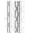
図6はR(赤)、G(緑)、B(青)カラー表示を行う画素配列の一例であり、R画素10、G画素20、B画素30の配列を示している。各画素にはTFT13、23、33と配線110〜112によってTFTと接続する透光性電極(陽極)113〜115が設けられている。カラーフィルターの着色層107〜109(Rフィルター107、Gフィルター108、Bフィルター109)はゲート信号線(走査信号線)102〜104より上層であり、データ信号線11、12、21、22、31よりも下層側に形成されている。そして、隣接する各着色層の境界領域は、ゲート信号線及びデータ線号線と重畳して設けられている。また、透光性電極113〜115は、各着色層107〜109の内側に重畳して設けられている。この画素構造において、A−A'線に対応する縦断面図を図1に示す。
【0029】
図1において、R画素10、G画素20、B画素30にはTFT13、23、33と、発光素子15、25、35が備えられ、その間に無機又は有機材料で形成される平坦化絶縁膜105が形成されている。平坦化絶縁膜105は平坦な表面を有し、その表面上にカラーフィルターの着色層107〜109が形成されている。カラーフィルターの着色層は、樹脂バインダー中の顔料、染料を分散させたものを塗布法により形成し、光露光工程を用いて所定のパターンに形成したものである。
【0030】
この着色層107〜109と平坦化絶縁膜105との間には、窒化珪素などのバリア性の絶縁膜106を形成しておく。これにより、着色層に含まれる顔料などの成分がTFT側に拡散するのを防ぐことができる。また、アルカリ水溶性現像液でパターン形成する際に、平坦化絶縁膜105やその下層のTFTがアルカリ成分で劣化するのを防ぐことができる。さらに、無機又は有機材料から成る平坦化面上にカラーフィルターの着色層を各色毎に形成することにより、高い位置合わせ精度をもって各着色層を配列させることができる。尚、ここでいうバリア性絶縁膜の機能は、イオン性不純物、水分、金属不純物、アルカリ金属などを遮蔽し拡散を阻止する機能を有している。
【0031】
また、平坦化絶縁膜105とTFT13、23、33の間には窒化珪素、窒酸化珪素、窒化アルミニウム、窒酸化アルミニウムから選ばれた材料で形成される無機絶縁膜103が形成される。これによりカラーフィルターの着色層の成分などがTFT内に拡散するのを防ぐことができる。
【0032】
発光素子15、25、35は、それそれ透光性電極(陽極)113〜115と非透光性電極(陰極)119との間に発光性を有する有機化合物層118を形成したものである。透光性電極(陽極)113〜115は酸化インジウムスズ(ITO)、酸化亜鉛(ZnO)、酸化インジウム亜鉛(IZO)など透光性導電膜を抵抗加熱蒸着法で形成する。非透光性電極(陰極)118はアルカリ金属又はアルカリ土類金属のフッ化物などで形成する。
【0033】
有機化合物層は様々な構成が可能であるが、陽極側にある正孔注入輸送層、陰極側にある電子注入輸送層、発光層等を適宜組み合わせた構造となっている。正孔注入輸送層又は電子注入輸送層は、電極からの正孔又は電子の注入効率と、輸送性(移動度)が特に重要な特性として着目されるものであるが、さらに発光層としての機能も兼ね備えた発光性電子注入輸送層などもあるとされている。
【0034】
これらの有機発光媒体又は各有機層は1種又は複数種の有機材料によって形成されるが、有機発光材料と電子注入輸送性材料及び又は正孔注入輸送材料との混合物や、当該混合物若しくは有機発光材料又は金属錯体を分散させた高分子材料などで形成されていれば良い。
【0035】
これらの各層を形成する有機化合物は、短分子系有機化合物と高分子系有機化合物の両者が知られている。短分子系有機化合物の一例は、正孔注入輸送層として銅フタロシアニン(CuPc)芳香族アミン系材料であるα−NPD(4,4'-ビス-[N-(ナフチル)-N-フェニル-アミノ]ビフェニル)やMTDATA(4,4',4"-トリス(N-3-メチルフェニル-N-フェニル-アミノ)トリフェニルアミン)、電子注入輸送層又は発光性電子注入輸送層としてトリス−8−キノリノラトアルミニウム錯体(Alq3)等が知られている。高分子系有機化合物材料では、ポリアニリンやポリチオフェン誘導体(PEDOT)等が適用できる。
【0036】
高分子系有機化合物材料で発光層を形成する場合には、π共役系材料を用いる。代表的な材料としては、ポリパラフェニレンビニレン(PPV)系、ポリビニルカルバゾール(PVK)系、ポリフルオレン系などである。具体的には、R画素にシアノポリフェニレンビニレン、G画素にシアノポリフェニレンビニレン、B画素にシアノポリフェニレンビニレン又はポリアルキルフェニレンを用いれば良い。尚、以上の材料は発光層として適用できる一例でありこれに限定される必要はない。勿論、白色の発光する材料で発光層を形成しても良い。
【0037】
白色発光を得る方法は、光の3原色であるR(赤)G(緑)B(青)の各色を発光する発光層を積層して加法混色する方式と、2色の補色の関係を利用する方式とがある。補色を用いる場合には、青−黄色又は青緑−橙色の組み合わせが知られている。特に、後者の方が比較的視感度の高い波長領域の発光を利用できる点で有利であると考えられている。
【0038】
白色発光を呈する発光素子の一例は、一対の陰極と陽極の間に、電子注入輸送層、赤色発光層、緑色発光層、正孔輸送層、青色発光層、第2電極を積層した構造である。正孔輸送層として1,2,4-トリアゾール誘導体(p−EtTAZ)、緑色発光層として用いるトリス(8−キノリラト)アルミニウム(Alq3)、青色発光層としてTPDの青色にAlq3の緑色が混ざった青緑色の発光が得る。この発光に赤色を加え白色発光を実現するには赤色発光層としてAlq3かTPDのどちらかに赤色発光色素をドープすれば良い。赤色発光色素としてはナイルレッドなどを適用することができる。
【0039】
また、他の構成として、電子注入輸送層、電子輸送層、発光層、正孔輸送層、正孔注入輸送層とすることもできる。この場合適した材料の組み合わせは、電子注入輸送層としてAlq3を用い、電子輸送層としてフェニルアントラセン誘導体を形成する。発光層はテトラアリールベンジジン誘導体とフェニルアントラセン誘導体とが体積比1:3で混合し、且つスチリルアミン誘導体を3体積%含ませる第1発光層と、テトラアリールベンジジン誘導体と10,10'−ビス[2-ビフェニルイル]−9,9'−ビアンスリル(フェニルアントラセン誘導体)とを体積比1:3で混合し、且つナフタセン誘導体を3重量%含ませる第2発光層とを積層させた構成とする。正孔輸送層はN,N,N',N'−テトラキス−(3-ビフェニル-1-イル)ベンジジン(テトラアリールベンジジン誘導体)を形成し、正孔注入層としてN,N'−ジフェニル-N,N'−ビス[N-フェニル-N-4-トリル(4-アミノフェニル)]ベンジジンを形成する。
【0040】
また、他の構成として、電子注入輸送層として電子輸送性の高いAlq3を用い、その上に高分子系有機発光媒体を用い、TAZ及びPVK(ポリ(N-ビニルカルバゾール))を形成した3層構造とする。注入された電子及び正孔の再結合はPVKで起こり、短波長にピークを持つカルバゾール基が励起され発光する。これに長波長光の発光を加えるために適当な色素をドープすると白色発光を得ることができる。例えば、1,1,4,4-テトラフェニル-1,3-ブタジエニン(TPB)を2〜3mol%ドープすることにより450nmの発光が得られ、緑や赤もクマリン6やDCM1をドープすることにより得ることができる。いずれにしても白色発光を得るには多種の色素をPVK中にドープして可視光域全体をカバーすれば良い。この構造において、電子注入輸送層203を無機電子注入輸送層を用いても良い。無機電子輸送層としてはn型化したダイヤモンドライクカーボン(DLC)を適用することができる。DLC膜のn型化には燐などを適宜ドープすれば良い。その他に、アルカリ金属元素、アルカリ土類金属元素、及びランタノイド系元素から選択される一種の酸化物と、Zn、Sn、V、Ru、Sm、Inから選択される1種以上の無機材料を適用することができる。
【0041】
また、他の構成として、4,4'-ビス-[N-(ナフチル)-N-フェニル-アミノ]ビフェニル(α−NPD)のみから成る正孔注入輸送層を形成し、その上にα−NPDと電子輸送性材料であるBAlqを混合させた発光層を形成し、その上にBAlqのみから成る電子注入輸送層を形成した構成としても良い。この発光層は青色の発光をするので、第2の発光材料として黄色蛍光色素であるルブレンを添加した領域を形成する。これにより白色発光を得ることができる。
【0042】
いずれにしても、視覚的に自然な白色発光を実現し、より高品質な多色表示をしようとする場合には、各色に発光する有機発光素子とカラーフィルターの組み合わせを最適化して色バランスを考慮する必要がある。また、発光輝度が経時変化する場合に対応して駆動回路側で便宜を図る必要がある。
【0043】
2色の補色の関係を利用する方式では、青−黄色又は青緑−橙色の組み合わせが通常適用されるので、それぞれに色の光を発光する有機発光素子が経時変化により劣化することにより色バランスが崩れるといった問題点がある。また、それぞれの有機発光素子の発光効率が違うので、同じ駆動電圧又は駆動電流を印加するのでは色バランスが崩れるといった問題点がある。
【0044】
通常はカラーフィルターの着色層の厚さを変えて透過光量を制御したり、画素の面積を変えて光量を制御したりする方法がある。しかし、着色層の厚さを変える場合には数μmの割合でその厚さを変える必要があり、対向基板として固着する場合に平坦化膜を厚くするかシール材の厚さを厚くする必要があり、封止構造における信頼性を損なう可能性がある。また、画素の面積を変える場合には、TFTの配置やサイズに制限があり、面積を有効に活用できないという弊害がある。
【0045】
隔壁層116は隣接する画素を分離するためのものであり、また透光性電極113〜115の端部で発光素子が短絡不良を起こすのを防いでいる。この形態において適した有機化合物層の構成は、PEDOT/PSSのような導電性ポリマー117を全面に塗布し、その上に発光層を含む有機化合物層118を形成したものである。この場合、導電性ポリマー117の厚さ形状は、隔壁116の影響によりその上部で薄く、隔壁層116の端部(即ち、隔壁層と透光性電極の接する部分)で厚くなる。これにより隔壁層上部における横方向の抵抗が高くなり、クロストークを防ぐことができる。さらに当該端部近傍においてが厚くなるため、電界集中を緩和し、画素端部からの劣化を防ぐことができる。またここにPEDOT/PSSのような導電性ポリマーを用いることにより、正孔注入特性が改善され、発光効率を向上させることができる。
【0046】
そして、発光素子15、25、35は、配線110〜112は、着色層107〜109、平坦化絶縁膜105、106を貫通してTFT13、23、33とそれぞれ接続している。
【0047】
さらに非透光性電極119上には保護膜120を窒化珪素又はダイヤモンドライクカーボン、水素化又はハロゲン化された、アモルファスカーボン(a−C:H)膜、アモルファスシリコン(a−Si)膜、ダイヤモンドライクカーボン(DLC)膜、アモルファス窒化シリコン膜などで被覆すると共に、これらの被膜をプラズマCVD法により形成して、プラズマ中の水素又はハロゲンにより有機化合物層を水素又はハロゲン化して欠陥を補償し、安定化させることができる。
【0048】
発光素子で発光する光は、カラーフィルターの着色層を透過して、基板101側から放射され視認することができる。基板は発光光を透過するものであれば様々なものが適用可能である。ガラスでは市販されている無アルカリガラスなどの透明ガラスが好ましく、表面を酸化珪素膜で被覆したアルカリガラスを適用することもできる。プラスチックを用いる場合には、ポリエチレンナフタレート(PEN)、ポリエチレンテレフタレート(PET)、ポリエーテルサルフォン(PES)、透光性のポリイミドなどを適用することができる。その他、透光性アルミナ、ZnS焼結体などの透明セラミックを適用することもできる。基板の形態は板状物、フィルム状物、シート状物のいずれの形態であっても良く、単層構造又は積層構造のいずれの構造を有していても良い。
【0049】
発光性を有する有機化合物層を発光させる場合、その分光スペクトルは比較的広い波長範囲に渡って分布して色純度が低下する。これを補正するためにカラーフィルターを用いることで、その色純度を向上させることが可能となる。勿論、発光素子が白色に発光する場合には、このカラーフィルターによりカラー表示を行うことができる。さらに、カラーフィルターを設けることで、非透光性電極の光反射により、図5で示すような形態の発光装置において、画素部が鏡面化するのを防ぐことができる。
【0050】
図4は図1の構成において、バリア性の絶縁膜121を着色層107〜109上に形成した例を示している。着色層上にバリア性の絶縁膜121を形成することにより、以降の工程において着色層に傷が付きにくくなり、また顔料成分が発光素子に拡散して素子を劣化させるのを防ぐことができる。
【0051】
一方、カラーフィルターの着色層の表面には微細な突起や、隣接する着色層どうしが重なり合う境界領域は、その厚さが他の領域より厚くなり凸部が形成される。特に前者が発光素子形成領域上、即ち画素面内にあるとそれに起因して短絡不良、黒点不良など好ましくない現象が発生し、特に高精細の表示画面を形成する場合においては表示品質の低下をもたらす原因となる。
【0052】
図2(A)は、無機又は有機絶縁材料による平坦化絶縁膜105及びバリア性の絶縁膜106上に着色層107〜109が形成され、前述の突起や凸部が形成された状態を示している。前述の突起や凸部を除去するためには、着色層を形成した後、機械的研磨、又はスラリーなどを併用して化学的機械研磨により突起や凸部を取り除いてしまうことが望ましい。図2(B)は研磨後の状態を示している。
【0053】
この状態で着色層のピンホール、ひび割れ、欠け、パターンずれなどの検査を行い、不良品を選別して再加工を行うことができる。
【0054】
その後、図3(A)に示すように窒化珪素などで形成するバリア性の無機絶縁膜121を、シリコンをターゲットとした高周波スパッタリング法で形成する。この窒化珪素膜を形成することで、着色層に含まれる顔料などの不純物が発光素子の有機化合物層に拡散し、素子特性を劣化させるのを防ぐことができる。
【0055】
図3(B)は発光素子まで形成した状態であり、その構成は図1と同様である。差異として、PEDOT/PSSのような導電性ポリマー117上に形成する発光層を含む有機化合物層118を、赤色発光用有機化合物層130、緑色発光用有機化合物層131、青色発光用有機化合物層132と個別に形成しても良い。非透光性電極(陰極)119と保護膜120の構成は図1と同様である。
【0056】
【発明の効果】
以上のように本発明において発光装置が基板上にTFT、カラーフィルター、発光素子が組み合わされ一体形成され、最高温度プロセスはTFTの構成部材である半導体層を結晶化させる600℃程度の温度、又は水素化を行う350〜450℃の温度であり、即ち平坦化膜の形成前である。従って、耐熱性が200℃程度しかないカラーフィルターの着色層は何ら問題なく作り込むことができる。また、TFT工程とカラーフィルター工程との歩留まりが積算されることなく、高精細で且つ製造コストの低減を可能とする発光装置を提供することができる。
【図面の簡単な説明】
【図1】 本発明のカラーフィルター着色層を備えた発光装置の構成を示す縦断面図。
【図2】 本発明のカラーフィルター着色層を備えた発光装置の作製工程を示す縦断面図。
【図3】 本発明のカラーフィルター着色層を備えた発光装置の作製工程を示す縦断面図。
【図4】 本発明のカラーフィルター着色層を備えた発光装置の構成を示す縦断面図。
【図5】 発光装置の構成を示す上面図。
【図6】 本発明のカラーフィルター着色層を備えた発光装置の画素の構成を示す上面図。[0001]
BACKGROUND OF THE INVENTION
The present invention relates to a method for manufacturing a light-emitting device including a light-emitting element having a layer made of an organic compound (hereinafter referred to as an organic compound layer), and particularly relates to a multicolor display function.
[0002]
[Prior art]
A self-luminous display device using a light-emitting element in which an organic compound layer is interposed between a pair of electrodes has been attracting attention as a next-generation display device because of its wide viewing angle and excellent visibility.
[0003]
The light-emitting mechanism of the light-emitting element is that excitons are obtained by recombining holes injected from one anode of a pair of electrodes and electrons injected from the other cathode in a light-emitting organic compound layer (light-emitting layer). This is considered as a phenomenon in which light is emitted when the exciton returns to the ground state. This light emission is called electroluminescence. Electroluminescence includes fluorescence and phosphorescence, and these include emission from a singlet state (fluorescence) in an excited state and emission from a triplet state (phosphorescence). Luminance by light emission is thousands to tens of thousands cd / m 2 Therefore, it is considered that it can be applied to a display device or the like in principle.
[0004]
In such a light emitting device, the organic thin film is usually formed as a thin film having a thickness of less than 1 μm. Further, since the light emitting element is a self-luminous element in which the organic thin film itself emits light, a backlight as used in a conventional liquid crystal display is not necessary. Therefore, it is a great advantage that the light-emitting element can be manufactured to be extremely thin and light.
[0005]
In a method called active matrix driving, a thin film transistor (TFT) is provided for each pixel, and light emission of the light emitting element is individually controlled to enable high-definition and crosstalk-free image display.
[0006]
In the method of color display, the materials or additives of the light emitting layer are made different, the light emitting color is arranged differently for each pixel, and the light emitting element that emits white light is used. A method of combining with a filter was known.
[0007]
[Problems to be solved by the invention]
However, if the color filter and the pixel matrix in which the light emitting elements are provided for each pixel are formed separately, it is necessary to align and assemble the two with high accuracy. There was a problem that the aperture ratio decreased.
[0008]
Of course, it is conceivable that the colored layer of the color filter is formed with the same alignment accuracy in the TFT substrate manufacturing process. However, since the heat resistant temperature is about 200 ° C., the TFT can withstand a process temperature of about 450 ° C. could not.
[0009]
In addition, a material called a color resist used for forming a colored layer of a color filter is a rather expensive material, and a process in which the yield of the TFT process and the color filter process is integrated becomes an increase factor of the manufacturing cost. There was a problem that it was not suitable.
[0010]
The present invention solves such problems, and an object thereof is to provide a light-emitting device with high definition and capable of reducing manufacturing costs.
[0011]
[Means for Solving the Problems]
In order to solve the above problems, the configuration of the present invention includes a TFT, a colored layer of a color filter, and a light emitting element in which an organic compound layer having a light emitting property is formed between a pair of electrodes on a substrate. In the light emitting device, the colored layer of the color filter is formed on a flat surface of an insulating film formed of an inorganic or organic material on the TFT, and light emitted from the light emitting element is emitted through the colored layer.
[0012]
In the present invention, a planarization insulating film made of an inorganic or organic material covering a TFT formed on a substrate is formed, a colored layer of a color filter is provided on a flat surface of the insulating film, and a pair of electrodes is formed on the colored layer. A light-emitting element having a light-emitting organic compound layer formed therebetween is provided, and light emission of the light-emitting element is emitted through the colored layer.
[0013]
In the present invention, a planarization insulating film made of an inorganic or organic material covering a TFT formed on a substrate is formed, a colored layer of a color filter is provided on a flat surface of the insulating film, and a pair of electrodes is formed on the colored layer. A light-emitting element having a light-emitting organic compound layer formed therebetween is provided, and the TFT and the light-emitting element are electrically connected by a wiring penetrating the insulating film and the colored layer, and light emission of the light-emitting element is emitted through the colored layer. It is what is done.
[0014]
In the present invention, a light emitting element in which a light emitting organic compound layer is formed between a pair of electrodes and TFTs are arranged in a matrix to form a pixel portion, and coloring of a color filter provided corresponding to each pixel The layer is provided in contact with the flat surface of the planarization insulating film made of an inorganic or organic material between the light emitting element and the TFT, and the boundary region of the adjacent colored layer is a gate signal line or data for sending a signal to the TFT. It is provided so as to overlap with the line.
[0015]
In the present invention, a light emitting element in which an organic compound layer having a light emitting property is formed between a pair of electrodes composed of a light transmitting electrode and a non-light transmitting electrode and TFTs are arranged in a matrix to form a pixel portion. The color layer of the color filter formed and provided corresponding to each pixel is provided in contact with the flat surface of the planarization insulating film made of an inorganic or organic material between the light emitting element and the TFT, and is adjacent to the color layer. The boundary region is provided so as to overlap with a gate signal line or a data line for sending a signal to the TFT, and the translucent electrode is provided so as to overlap the inside of the colored layer.
[0016]
The planarization insulating film made of an inorganic or organic material is formed of an inorganic insulating film such as silicon oxide, polyimide, acrylic, or the like. The colored layer may be formed on the planarization insulating film, or an inorganic insulating film such as silicon nitride may be interposed therebetween. On the colored layer of the color filter, a translucent electrode (anode) formed as an individual electrode for each pixel is formed. Further, an inorganic insulating film such as a silicon nitride film may be formed between the translucent electrode (anode) and the colored layer.
[0017]
In the light emitting element, an organic compound layer is laminated using the translucent electrode (anode) as one electrode, and the other electrode facing the translucent electrode (anode) is formed thereon. With such a light emitting element structure, light emission is emitted from the translucent electrode (anode) side, that is, the light can be taken out through the colored layer of the color filter.
[0018]
The boundary region between the adjacent colored layers is provided at a position overlapping with the gate signal line or the data line number line provided in the pixel portion, and the wiring can be used as a light shielding film, so that the aperture ratio can be improved.
[0019]
The organic compound layer has a structure in which a hole injection / transport layer on the anode side, an electron injection / transport layer on the cathode side, a light emitting layer, and the like are appropriately combined. The hole injecting and transporting layer or the electron injecting and transporting layer is a material in which the efficiency of injecting holes or electrons from the electrode and the transportability (mobility) are particularly important characteristics. A luminescent electron injecting and transporting layer that also has a combination may be combined.
[0020]
As the organic compounds forming these layers, both short molecular organic compounds and high molecular organic compounds are known. An example of a short organic compound is α-NPD (4,4′-bis- [N- (naphthyl) -N-phenyl-amino) which is a copper phthalocyanine (CuPc) aromatic amine material as a hole injection transport layer. ] Biphenyl), MTDATA (4,4 ', 4 "-tris (N-3-methylphenyl-N-phenyl-amino) triphenylamine), tris-8- as an electron injecting and transporting layer or a luminescent electron injecting and transporting layer Quinolinolato aluminum complex (Alq Three ) Etc. are known. As the polymer organic light emitting material, polyaniline, polythiophene derivative (PEDOT) and the like are known.
[0021]
The colored layer of the color filter is formed by applying a dispersion of pigments and dyes in a resin binder by a coating method, and is formed into a predetermined pattern using a light exposure process. In this case, each colored layer can be arranged with high alignment accuracy by forming the colored layer of the color filter for each color on the flattened surface made of an inorganic or organic material.
[0022]
In addition, the colored layer to be patterned with an alkaline water-soluble developer is arranged before the contact hole is formed in the planarization insulating layer, so that the semiconductor film is not contaminated by alkali components, pigments, dyes, or the like.
[0023]
Further, by interposing an inorganic insulating film such as silicon nitride between the planarizing film and the colored layer, it is possible to prevent components such as a pigment contained in the colored layer from diffusing to the TFT side. In addition, by forming an inorganic insulating film such as a silicon nitride film between the translucent electrode (anode) and the colored layer, it is possible to prevent components such as pigments contained in the colored layer from diffusing on the light emitting element side. be able to.
[0024]
Further, the surface of the colored layer of the color filter may be polished and flattened. Thereby, the yield of the color filter can be improved, and at the same time, the flatness of the surface of the translucent electrode (anode) formed thereon can be improved, and the short circuit of the light emitting element can be prevented.
[0025]
In any case, by forming a colored layer of the color filter on the flattened layer, pinhole inspection of the colored layer can be performed at this stage, and those that do not meet the predetermined standard are peeled off. Can be reworked. As a peeling method, it may be removed by washing with a solvent, or may be mechanically polished and scraped off. In any case, since there is a planarization film, reprocessing can be performed without damaging the TFT.
[0026]
DETAILED DESCRIPTION OF THE INVENTION
Hereinafter, embodiments of the present invention will be described in detail with reference to the drawings. FIG. 5 illustrates one mode of a light emitting device in which a substrate 900 includes a pixel portion 902, gate signal side driver circuits 901a and 901b, a data signal side driver circuit 901c, an input / output terminal portion 935, and a wiring or a wiring group 917. Yes. The seal pattern 940 may partially overlap with the gate signal line side driving circuits 901a and 901b, the data signal line side driving circuit 901c, and the wiring or wiring group 917 that connects the driving circuit portion and the input terminal. In this way, the area of the frame region (the peripheral region of the pixel portion) of the display panel can be reduced. An FPC 936 is fixed to the external input terminal portion.
[0027]
The pixel portion 902 includes a TFT and a light emitting element provided for each pixel, and is arranged in a matrix. A top view of the pixel is shown in FIG. Note that FIG. 6 does not show each layer and the partition layer forming the light emitting element for the sake of explanation.
[0028]
FIG. 6 shows an example of a pixel array that performs R (red), G (green), and B (blue) color display, and shows an array of the
[0029]
In FIG. 1, the
[0030]
A
[0031]
In addition, an inorganic
[0032]
Each of the light-emitting
[0033]
The organic compound layer can have various configurations, but has a structure in which a hole injection / transport layer on the anode side, an electron injection / transport layer on the cathode side, a light emitting layer, and the like are appropriately combined. The hole injecting and transporting layer or the electron injecting and transporting layer is a material in which the efficiency of injecting holes or electrons from the electrode and the transportability (mobility) are particularly important characteristics. It is also said that there is a luminescent electron injecting and transporting layer that also has both.
[0034]
These organic light-emitting media or each organic layer is formed of one or more kinds of organic materials, and a mixture of an organic light-emitting material and an electron injecting and transporting material and / or a hole injecting and transporting material, the mixture or organic light emitting What is necessary is just to be formed with the polymeric material etc. which disperse | distributed material or a metal complex.
[0035]
As the organic compounds forming these layers, both short molecular organic compounds and high molecular organic compounds are known. An example of a short organic compound is α-NPD (4,4′-bis- [N- (naphthyl) -N-phenyl-amino) which is a copper phthalocyanine (CuPc) aromatic amine material as a hole injection transport layer. ] Biphenyl), MTDATA (4,4 ', 4 "-tris (N-3-methylphenyl-N-phenyl-amino) triphenylamine), tris-8- as an electron injecting and transporting layer or a luminescent electron injecting and transporting layer Quinolinolato aluminum complex (Alq Three ) Etc. are known. For the polymer organic compound material, polyaniline, polythiophene derivative (PEDOT), or the like can be applied.
[0036]
In the case where the light emitting layer is formed of a high molecular organic compound material, a π-conjugated material is used. Typical materials include polyparaphenylene vinylene (PPV), polyvinyl carbazole (PVK), and polyfluorene. Specifically, cyanopolyphenylene vinylene may be used for the R pixel, cyanopolyphenylene vinylene for the G pixel, and cyanopolyphenylene vinylene or polyalkylphenylene for the B pixel. Note that the above materials are examples that can be applied as the light emitting layer, and need not be limited thereto. Of course, the light emitting layer may be formed of a material that emits white light.
[0037]
The method of obtaining white light emission utilizes the relationship between additive color mixing by laminating light emitting layers that emit light of the three primary colors R (red), G (green), and B (blue), and two complementary colors. There is a method to do. When complementary colors are used, combinations of blue-yellow or blue-green-orange are known. In particular, the latter is considered advantageous in that it can utilize light emission in a wavelength region with relatively high visibility.
[0038]
An example of a light-emitting element that exhibits white light emission has a structure in which an electron injection transport layer, a red light-emitting layer, a green light-emitting layer, a hole transport layer, a blue light-emitting layer, and a second electrode are stacked between a pair of a cathode and an anode. . 1,2,4-triazole derivative (p-EtTAZ) as a hole transport layer, tris (8-quinolinato) aluminum (Alq) used as a green light emitting layer Three ), Alq in blue of TPD as blue light emitting layer Three A blue-green light emission with a mixed green color is obtained. In order to realize white light emission by adding red to this light emission, Alq is used as a red light emitting layer. Three Or TPD may be doped with a red luminescent dye. Nile red or the like can be applied as the red light emitting pigment.
[0039]
As other configurations, an electron injecting and transporting layer, an electron transporting layer, a light emitting layer, a hole transporting layer, and a hole injecting and transporting layer can be used. In this case, a suitable material combination is Alq as the electron injection transport layer. Three Is used to form a phenylanthracene derivative as the electron transport layer. The light-emitting layer includes a first light-emitting layer in which a tetraarylbenzidine derivative and a phenylanthracene derivative are mixed at a volume ratio of 1: 3 and 3% by volume of a styrylamine derivative is contained, a tetraarylbenzidine derivative and 10,10′-bis [ 2-biphenylyl] -9,9′-bianthryl (phenylanthracene derivative) is mixed at a volume ratio of 1: 3, and a second light-emitting layer containing 3% by weight of a naphthacene derivative is laminated. The hole transport layer forms N, N, N ′, N′-tetrakis- (3-biphenyl-1-yl) benzidine (tetraarylbenzidine derivative), and N, N′-diphenyl-N as the hole injection layer , N′-bis [N-phenyl-N-4-tolyl (4-aminophenyl)] benzidine.
[0040]
Further, as another configuration, Alq having a high electron transport property as an electron injection transport layer. Three And a polymer organic light-emitting medium is used to form a three-layer structure in which TAZ and PVK (poly (N-vinylcarbazole)) are formed. Recombination of injected electrons and holes occurs in PVK, and a carbazole group having a peak at a short wavelength is excited to emit light. White light emission can be obtained by doping an appropriate dye to add long-wavelength light. For example, light emission of 450 nm can be obtained by doping 2-3 mol% of 1,1,4,4-tetraphenyl-1,3-butadienin (TPB), and green and red can also be doped by coumarin 6 or DCM1. Obtainable. In any case, in order to obtain white light emission, various dyes may be doped into PVK to cover the entire visible light region. In this structure, the electron injecting and transporting layer 203 may be an inorganic electron injecting and transporting layer. As the inorganic electron transport layer, n-type diamond-like carbon (DLC) can be applied. Phosphorus or the like may be appropriately doped to make the DLC film n-type. In addition, one kind of oxide selected from alkali metal elements, alkaline earth metal elements, and lanthanoid elements and one or more inorganic materials selected from Zn, Sn, V, Ru, Sm, and In are applied. can do.
[0041]
As another configuration, a hole injecting and transporting layer composed only of 4,4′-bis- [N- (naphthyl) -N-phenyl-amino] biphenyl (α-NPD) is formed, and α- A light emitting layer in which NPD and BAlq which is an electron transporting material are mixed may be formed, and an electron injection transport layer made only of BAlq may be formed thereon. Since this light emitting layer emits blue light, a region to which rubrene, which is a yellow fluorescent dye, is added as a second light emitting material is formed. Thereby, white light emission can be obtained.
[0042]
In any case, to achieve visually natural white light emission and to achieve higher-quality multicolor display, the color balance is optimized by optimizing the combination of organic light-emitting elements that emit light in each color and color filters. It is necessary to consider. In addition, it is necessary to provide convenience on the drive circuit side in response to the case where the emission luminance changes with time.
[0043]
In the method utilizing the relationship between the two complementary colors, a combination of blue-yellow or blue-green-orange is usually applied, so that the organic light-emitting element that emits light of each color deteriorates with time, so that the color balance is reduced. There is a problem that collapses. In addition, since the light emitting efficiency of each organic light emitting element is different, there is a problem that the color balance is lost if the same driving voltage or driving current is applied.
[0044]
Usually, there are methods of controlling the amount of transmitted light by changing the thickness of the colored layer of the color filter, or controlling the amount of light by changing the area of the pixel. However, when changing the thickness of the colored layer, it is necessary to change the thickness at a rate of several μm, and when fixing as a counter substrate, it is necessary to increase the thickness of the planarizing film or the thickness of the sealing material. There is a possibility that reliability in the sealing structure is impaired. In addition, when the area of the pixel is changed, there is a limitation that the arrangement and size of the TFT are limited, and the area cannot be effectively used.
[0045]
The
[0046]
In the
[0047]
Further, a
[0048]
Light emitted from the light-emitting element is transmitted through the colored layer of the color filter and is emitted from the
[0049]
When an organic compound layer having a light emitting property is caused to emit light, its spectral spectrum is distributed over a relatively wide wavelength range and color purity is lowered. By using a color filter to correct this, the color purity can be improved. Needless to say, when the light emitting element emits white light, color display can be performed by this color filter. Further, by providing a color filter, it is possible to prevent the pixel portion from being mirror-finished in the light-emitting device having the configuration shown in FIG. 5 due to light reflection of the non-transparent electrode.
[0050]
FIG. 4 shows an example in which a
[0051]
On the other hand, the surface of the colored layer of the color filter has fine protrusions and a boundary region where adjacent colored layers overlap with each other, so that the thickness thereof is thicker than other regions and a convex portion is formed. In particular, when the former is on the light emitting element formation region, that is, within the pixel surface, undesired phenomena such as short circuit failure and black spot failure occur, and display quality is deteriorated particularly when a high-definition display screen is formed. Cause.
[0052]
FIG. 2A shows a state in which the
[0053]
In this state, inspection of pinholes, cracks, chips, pattern deviation, etc. of the colored layer can be performed, and defective products can be selected and reprocessed.
[0054]
After that, as shown in FIG. 3A, a barrier inorganic insulating
[0055]
FIG. 3B shows a state where even the light emitting element is formed, and the structure thereof is the same as FIG. As a difference, an
[0056]
【The invention's effect】
As described above, in the present invention, the light emitting device is integrally formed on the substrate by combining the TFT, the color filter, and the light emitting element, and the maximum temperature process is a temperature of about 600 ° C. for crystallizing the semiconductor layer that is a constituent member of the TFT, or The temperature is 350 to 450 ° C. at which hydrogenation is performed, that is, before the formation of the planarizing film. Therefore, a colored layer of a color filter having a heat resistance of only about 200 ° C. can be formed without any problem. In addition, it is possible to provide a light-emitting device that can achieve high definition and reduce manufacturing costs without accumulating the yield of the TFT process and the color filter process.
[Brief description of the drawings]
FIG. 1 is a longitudinal cross-sectional view illustrating a configuration of a light-emitting device including a color filter coloring layer according to the present invention.
FIG. 2 is a longitudinal sectional view showing a manufacturing process of a light-emitting device provided with a color filter coloring layer of the present invention.
FIG. 3 is a longitudinal sectional view showing a manufacturing process of a light-emitting device provided with a color filter coloring layer of the present invention.
FIG. 4 is a vertical cross-sectional view illustrating a configuration of a light emitting device including a color filter coloring layer according to the present invention.
FIG 5 is a top view illustrating a structure of a light-emitting device.
FIG. 6 is a top view illustrating a structure of a pixel of a light-emitting device provided with a color filter coloring layer of the present invention.
Claims (1)
前記第1乃至第3の薄膜トランジスタ上に平坦化絶縁膜を形成し、
前記平坦化絶縁膜上に第1のバリア性の絶縁膜を形成し、
前記第1のバリア性の絶縁膜上に第1乃至第3のカラーフィルターを形成し、
前記第1のカラーフィルターと前記第2のカラーフィルタとの境界領域に形成された第1の凸部と、前記第2のカラーフィルターと前記第3のカラーフィルタとの境界領域に形成された第2の凸部と、を除去し、
前記第1乃至第3のカラーフィルター上に第2のバリア性の絶縁膜を形成し、
前記第2のバリア性の絶縁膜、前記第1のカラーフィルター、前記第1のバリア性の絶縁膜、及び前記平坦化絶縁膜を貫通し前記第1の薄膜トランジスタに達する第1のコンタクトホールと、前記第2のバリア性の絶縁膜、前記第2のカラーフィルター、前記第1のバリア性の絶縁膜、及び前記平坦化絶縁膜を貫通し前記第2の薄膜トランジスタに達する第2のコンタクトホールと、前記第2のバリア性の絶縁膜、前記第3のカラーフィルター、前記第1のバリア性の絶縁膜、及び前記平坦化絶縁膜を貫通し前記第3の薄膜トランジスタに達する第3のコンタクトホールと、を形成し、
前記第2のバリア性の絶縁膜上に、第1及び第2のデータ信号線と、前記第1のコンタクトホールを介して前記第1の薄膜トランジスタと電気的に接続される第1の配線と、前記第1の配線と電気的に接続される第1の透光性電極と、前記第2のコンタクトホールを介して前記第2の薄膜トランジスタと電気的に接続される第2の配線と、前記第2の配線と電気的に接続される第2の透光性電極と、前記第3のコンタクトホールを介して前記第3の薄膜トランジスタと電気的に接続される第3の配線と、前記第3の配線と電気的に接続される第3の透光性電極と、を形成し、
前記第1乃至第3の透光性電極の端部を覆う隔壁層を形成し、
導電性ポリマーを全面に塗布することにより、前記隔壁層上及び前記第1乃至第3の透光性電極上に導電性ポリマー層を形成し、
前記導電性ポリマー層上に第1乃至第3の有機化合物層を形成し、
前記第1乃至第3の有機化合物層上に非透光性電極を形成し、
前記第1の有機化合物層は赤色発光するとともに、赤色の前記第1のカラーフィルター及び前記第1の透光性電極と重なる位置に配置され、
前記第2の有機化合物層は緑色発光するとともに、緑色の前記第2のカラーフィルター及び前記第2の透光性電極と重なる位置に配置され、
前記第3の有機化合物層は青色発光するとともに、青色の前記第3のカラーフィルター及び前記第3の透光性電極と重なる位置に配置され、
前記第1乃至第3のカラーフィルターと前記第1乃至第3の透光性電極との間に形成された前記第2のバリア性の絶縁膜は、窒化珪素膜であり、
前記第1のデータ信号線は、前記第1の凸部が除去された境界領域と重なる位置に配置され、
前記第2のデータ信号線は、前記第2の凸部が除去された境界領域と重なる位置に配置されることを特徴とする発光装置の作製方法。Forming first to third thin film transistors on a substrate;
Forming a planarization insulating film on the first to third thin film transistors;
Forming a first barrier insulating film on the planarizing insulating film;
Forming first to third color filters on the first barrier insulating film;
A first protrusion formed in a boundary region between the first color filter and the second color filter; and a first protrusion formed in a boundary region between the second color filter and the third color filter. 2 protrusions ,
Forming a second barrier insulating film on the first to third color filters;
Said second barrier insulating film, the first color filter, the first contact hole first barrier insulating film, and the flattening insulating film to penetrate reach the first thin film transistor, A second contact hole penetrating through the second barrier insulating film, the second color filter, the first barrier insulating film, and the planarizing insulating film to reach the second thin film transistor; A third contact hole penetrating through the second barrier insulating film, the third color filter, the first barrier insulating film, and the planarizing insulating film to reach the third thin film transistor; Form the
On the second barrier insulating film, a first wiring connected with the first and second data signal lines, the first contact hole electrically with said first thin film transistor via, a first light-transmitting electrode connected said first wiring electrically, and a second wiring connected to the second contact holes electrically to the said second thin film transistor through the first A second translucent electrode electrically connected to the second wiring, a third wiring electrically connected to the third thin film transistor through the third contact hole, and the third wiring Forming a third translucent electrode electrically connected to the wiring ;
Forming a partition layer covering an end portion of the first to third translucent electrodes;
By applying a conductive polymer to the entire surface, a conductive polymer layer is formed on the partition wall layer and the first to third translucent electrodes,
Forming first to third organic compound layers on the conductive polymer layer;
A non-translucent electrode is formed on the first to third organic compound layers;
The first organic compound layer emits red light and is disposed at a position overlapping the red first color filter and the first light-transmitting electrode,
The second organic compound layer emits green light and is disposed at a position overlapping with the second color filter and the second light-transmitting electrode in green.
The third organic compound layer emits blue light and is disposed at a position overlapping the blue third color filter and the third translucent electrode,
The second barrier insulating film formed between the first to third color filters and the first to third translucent electrodes is a silicon nitride film;
The first data signal line is disposed at a position overlapping the boundary region from which the first convex portion is removed ,
The second data signal lines, a method for manufacturing a light-emitting device according to claim Rukoto is disposed at a position overlapping with the second boundary area where the convex portion is removed.
Priority Applications (1)
| Application Number | Priority Date | Filing Date | Title |
|---|---|---|---|
| JP2003033891A JP4718761B2 (en) | 2002-02-13 | 2003-02-12 | Method for manufacturing light emitting device |
Applications Claiming Priority (4)
| Application Number | Priority Date | Filing Date | Title |
|---|---|---|---|
| JP2002-34919 | 2002-02-13 | ||
| JP2002034919 | 2002-02-13 | ||
| JP2002034919 | 2002-02-13 | ||
| JP2003033891A JP4718761B2 (en) | 2002-02-13 | 2003-02-12 | Method for manufacturing light emitting device |
Publications (3)
| Publication Number | Publication Date |
|---|---|
| JP2003308976A JP2003308976A (en) | 2003-10-31 |
| JP2003308976A5 JP2003308976A5 (en) | 2006-03-02 |
| JP4718761B2 true JP4718761B2 (en) | 2011-07-06 |
Family
ID=29405098
Family Applications (1)
| Application Number | Title | Priority Date | Filing Date |
|---|---|---|---|
| JP2003033891A Expired - Fee Related JP4718761B2 (en) | 2002-02-13 | 2003-02-12 | Method for manufacturing light emitting device |
Country Status (1)
| Country | Link |
|---|---|
| JP (1) | JP4718761B2 (en) |
Families Citing this family (12)
| Publication number | Priority date | Publication date | Assignee | Title |
|---|---|---|---|---|
| KR100667062B1 (en) | 2003-11-29 | 2007-01-10 | 삼성에스디아이 주식회사 | Donor film for laser induced thermal imaging method and electroluminescence display device manufactured using the same film |
| US7202504B2 (en) * | 2004-05-20 | 2007-04-10 | Semiconductor Energy Laboratory Co., Ltd. | Light-emitting element and display device |
| KR100755398B1 (en) | 2004-05-21 | 2007-09-04 | 엘지전자 주식회사 | Organic Electro-luminescence Display Device and Method For Fabricating Thereof |
| KR100721569B1 (en) * | 2004-12-10 | 2007-05-23 | 삼성에스디아이 주식회사 | Organic Electroluminescence Device Having Color Filter Layer |
| JP2006252775A (en) * | 2005-03-07 | 2006-09-21 | Ricoh Co Ltd | Display device |
| US7675078B2 (en) | 2005-09-14 | 2010-03-09 | Chunghwa Picture Tubes, Ltd. | Pixel structure |
| WO2010004944A1 (en) * | 2008-07-10 | 2010-01-14 | Semiconductor Energy Laboratory Co., Ltd. | Light-emitting device and electronic device using the same |
| KR20220038542A (en) * | 2009-10-21 | 2022-03-28 | 가부시키가이샤 한도오따이 에네루기 켄큐쇼 | Analog circuit and semiconductor device |
| US8890187B2 (en) * | 2010-04-16 | 2014-11-18 | Semiconductor Energy Laboratory Co., Ltd. | Light-emitting device with an insulating partition |
| KR101950830B1 (en) * | 2011-12-26 | 2019-04-26 | 엘지디스플레이 주식회사 | Organic light emitting display device and method for fabricating the same |
| TWI642170B (en) | 2013-10-18 | 2018-11-21 | 半導體能源研究所股份有限公司 | Display device and electronic device |
| JP6190709B2 (en) * | 2013-12-04 | 2017-08-30 | 株式会社ジャパンディスプレイ | Organic electroluminescence display device |
-
2003
- 2003-02-12 JP JP2003033891A patent/JP4718761B2/en not_active Expired - Fee Related
Also Published As
| Publication number | Publication date |
|---|---|
| JP2003308976A (en) | 2003-10-31 |
Similar Documents
| Publication | Publication Date | Title |
|---|---|---|
| US7397180B2 (en) | Light emitting device having a conductive polymer and coloring layers | |
| KR100849314B1 (en) | Active organic el device and method of manufacture thereof | |
| JP5254469B2 (en) | Image display device, panel and panel manufacturing method | |
| CN1604696B (en) | Light emitting device | |
| JP4163567B2 (en) | Light-emitting display device | |
| JP5356532B2 (en) | LIGHT EMITTING PANEL DEVICE CONNECTED BY MULTIPLE PANELS WITH LIGHT EMITTING UNIT, IMAGE DISPLAY DEVICE AND LIGHTING DEVICE EQUIPPED | |
| JP5094477B2 (en) | Organic light-emitting display device and method for manufacturing the same | |
| JP4507611B2 (en) | ORGANIC ELECTROLUMINESCENCE DEVICE AND ELECTRONIC DEVICE | |
| WO2012026209A1 (en) | Organic light emitting device and antistatic method for same | |
| JP4785911B2 (en) | Organic light emitting display | |
| US7948160B2 (en) | Optical device and manufacturing method of the optical device | |
| CN100511680C (en) | Semiconductor device and flat panel display comprising the same | |
| KR20160059563A (en) | Organice light emitting diode display | |
| US6864639B2 (en) | Display and method for manufacturing the same | |
| JP4718761B2 (en) | Method for manufacturing light emitting device | |
| JP2010277949A (en) | Organic el display device and method of manufacturing the same | |
| US9293740B2 (en) | Method of manufacturing EL display device | |
| US9209402B2 (en) | Method of manufacturing EL display device | |
| JP4314000B2 (en) | Display device | |
| KR101222985B1 (en) | Organic Emtting Device |
Legal Events
| Date | Code | Title | Description |
|---|---|---|---|
| A521 | Request for written amendment filed |
Free format text: JAPANESE INTERMEDIATE CODE: A523 Effective date: 20060118 |
|
| A621 | Written request for application examination |
Free format text: JAPANESE INTERMEDIATE CODE: A621 Effective date: 20060118 |
|
| A977 | Report on retrieval |
Free format text: JAPANESE INTERMEDIATE CODE: A971007 Effective date: 20081021 |
|
| A131 | Notification of reasons for refusal |
Free format text: JAPANESE INTERMEDIATE CODE: A131 Effective date: 20081028 |
|
| A521 | Request for written amendment filed |
Free format text: JAPANESE INTERMEDIATE CODE: A523 Effective date: 20081106 |
|
| A131 | Notification of reasons for refusal |
Free format text: JAPANESE INTERMEDIATE CODE: A131 Effective date: 20090303 |
|
| A02 | Decision of refusal |
Free format text: JAPANESE INTERMEDIATE CODE: A02 Effective date: 20090908 |
|
| A521 | Request for written amendment filed |
Free format text: JAPANESE INTERMEDIATE CODE: A523 Effective date: 20110207 |
|
| A01 | Written decision to grant a patent or to grant a registration (utility model) |
Free format text: JAPANESE INTERMEDIATE CODE: A01 |
|
| A61 | First payment of annual fees (during grant procedure) |
Free format text: JAPANESE INTERMEDIATE CODE: A61 Effective date: 20110401 |
|
| R150 | Certificate of patent or registration of utility model |
Ref document number: 4718761 Country of ref document: JP Free format text: JAPANESE INTERMEDIATE CODE: R150 Free format text: JAPANESE INTERMEDIATE CODE: R150 |
|
| FPAY | Renewal fee payment (event date is renewal date of database) |
Free format text: PAYMENT UNTIL: 20140408 Year of fee payment: 3 |
|
| FPAY | Renewal fee payment (event date is renewal date of database) |
Free format text: PAYMENT UNTIL: 20140408 Year of fee payment: 3 |
|
| R250 | Receipt of annual fees |
Free format text: JAPANESE INTERMEDIATE CODE: R250 |
|
| R250 | Receipt of annual fees |
Free format text: JAPANESE INTERMEDIATE CODE: R250 |
|
| R250 | Receipt of annual fees |
Free format text: JAPANESE INTERMEDIATE CODE: R250 |
|
| R250 | Receipt of annual fees |
Free format text: JAPANESE INTERMEDIATE CODE: R250 |
|
| R250 | Receipt of annual fees |
Free format text: JAPANESE INTERMEDIATE CODE: R250 |
|
| R250 | Receipt of annual fees |
Free format text: JAPANESE INTERMEDIATE CODE: R250 |
|
| R250 | Receipt of annual fees |
Free format text: JAPANESE INTERMEDIATE CODE: R250 |
|
| R250 | Receipt of annual fees |
Free format text: JAPANESE INTERMEDIATE CODE: R250 |
|
| LAPS | Cancellation because of no payment of annual fees |