JP4712474B2 - Semiconductor device, semiconductor device manufacturing method, semiconductor device manufacturing method program, and semiconductor manufacturing apparatus - Google Patents
Semiconductor device, semiconductor device manufacturing method, semiconductor device manufacturing method program, and semiconductor manufacturing apparatus Download PDFInfo
- Publication number
- JP4712474B2 JP4712474B2 JP2005221691A JP2005221691A JP4712474B2 JP 4712474 B2 JP4712474 B2 JP 4712474B2 JP 2005221691 A JP2005221691 A JP 2005221691A JP 2005221691 A JP2005221691 A JP 2005221691A JP 4712474 B2 JP4712474 B2 JP 4712474B2
- Authority
- JP
- Japan
- Prior art keywords
- unit
- semiconductor device
- adjustment
- test
- pads
- Prior art date
- Legal status (The legal status is an assumption and is not a legal conclusion. Google has not performed a legal analysis and makes no representation as to the accuracy of the status listed.)
- Expired - Fee Related
Links
Images


Classifications
-
- G—PHYSICS
- G01—MEASURING; TESTING
- G01P—MEASURING LINEAR OR ANGULAR SPEED, ACCELERATION, DECELERATION, OR SHOCK; INDICATING PRESENCE, ABSENCE, OR DIRECTION, OF MOVEMENT
- G01P15/00—Measuring acceleration; Measuring deceleration; Measuring shock, i.e. sudden change of acceleration
- G01P15/18—Measuring acceleration; Measuring deceleration; Measuring shock, i.e. sudden change of acceleration in two or more dimensions
-
- G—PHYSICS
- G01—MEASURING; TESTING
- G01P—MEASURING LINEAR OR ANGULAR SPEED, ACCELERATION, DECELERATION, OR SHOCK; INDICATING PRESENCE, ABSENCE, OR DIRECTION, OF MOVEMENT
- G01P15/00—Measuring acceleration; Measuring deceleration; Measuring shock, i.e. sudden change of acceleration
- G01P15/02—Measuring acceleration; Measuring deceleration; Measuring shock, i.e. sudden change of acceleration by making use of inertia forces using solid seismic masses
- G01P15/08—Measuring acceleration; Measuring deceleration; Measuring shock, i.e. sudden change of acceleration by making use of inertia forces using solid seismic masses with conversion into electric or magnetic values
- G01P15/0802—Details
-
- G—PHYSICS
- G01—MEASURING; TESTING
- G01P—MEASURING LINEAR OR ANGULAR SPEED, ACCELERATION, DECELERATION, OR SHOCK; INDICATING PRESENCE, ABSENCE, OR DIRECTION, OF MOVEMENT
- G01P15/00—Measuring acceleration; Measuring deceleration; Measuring shock, i.e. sudden change of acceleration
- G01P15/02—Measuring acceleration; Measuring deceleration; Measuring shock, i.e. sudden change of acceleration by making use of inertia forces using solid seismic masses
- G01P15/08—Measuring acceleration; Measuring deceleration; Measuring shock, i.e. sudden change of acceleration by making use of inertia forces using solid seismic masses with conversion into electric or magnetic values
- G01P15/12—Measuring acceleration; Measuring deceleration; Measuring shock, i.e. sudden change of acceleration by making use of inertia forces using solid seismic masses with conversion into electric or magnetic values by alteration of electrical resistance
- G01P15/123—Measuring acceleration; Measuring deceleration; Measuring shock, i.e. sudden change of acceleration by making use of inertia forces using solid seismic masses with conversion into electric or magnetic values by alteration of electrical resistance by piezo-resistive elements, e.g. semiconductor strain gauges
-
- G—PHYSICS
- G01—MEASURING; TESTING
- G01P—MEASURING LINEAR OR ANGULAR SPEED, ACCELERATION, DECELERATION, OR SHOCK; INDICATING PRESENCE, ABSENCE, OR DIRECTION, OF MOVEMENT
- G01P15/00—Measuring acceleration; Measuring deceleration; Measuring shock, i.e. sudden change of acceleration
- G01P15/02—Measuring acceleration; Measuring deceleration; Measuring shock, i.e. sudden change of acceleration by making use of inertia forces using solid seismic masses
- G01P15/08—Measuring acceleration; Measuring deceleration; Measuring shock, i.e. sudden change of acceleration by making use of inertia forces using solid seismic masses with conversion into electric or magnetic values
- G01P2015/0805—Measuring acceleration; Measuring deceleration; Measuring shock, i.e. sudden change of acceleration by making use of inertia forces using solid seismic masses with conversion into electric or magnetic values being provided with a particular type of spring-mass-system for defining the displacement of a seismic mass due to an external acceleration
- G01P2015/0822—Measuring acceleration; Measuring deceleration; Measuring shock, i.e. sudden change of acceleration by making use of inertia forces using solid seismic masses with conversion into electric or magnetic values being provided with a particular type of spring-mass-system for defining the displacement of a seismic mass due to an external acceleration for defining out-of-plane movement of the mass
- G01P2015/084—Measuring acceleration; Measuring deceleration; Measuring shock, i.e. sudden change of acceleration by making use of inertia forces using solid seismic masses with conversion into electric or magnetic values being provided with a particular type of spring-mass-system for defining the displacement of a seismic mass due to an external acceleration for defining out-of-plane movement of the mass the mass being suspended at more than one of its sides, e.g. membrane-type suspension, so as to permit multi-axis movement of the mass
- G01P2015/0842—Measuring acceleration; Measuring deceleration; Measuring shock, i.e. sudden change of acceleration by making use of inertia forces using solid seismic masses with conversion into electric or magnetic values being provided with a particular type of spring-mass-system for defining the displacement of a seismic mass due to an external acceleration for defining out-of-plane movement of the mass the mass being suspended at more than one of its sides, e.g. membrane-type suspension, so as to permit multi-axis movement of the mass the mass being of clover leaf shape
Description
本発明は、微小構造体たとえばMEMS(Micro Electro Mechanical Systems)を有する半導体装置、その製造方法およびその製造方法プログラムおよび半導体製造装置に関する。 The present invention relates to a semiconductor device having a microstructure such as MEMS (Micro Electro Mechanical Systems), a manufacturing method thereof, a manufacturing method program thereof, and a semiconductor manufacturing device.
近年、特に半導体微細加工技術等を用いて、機械・電子・光・化学等の多用な機能を集積化したデバイスであるMEMSが注目されている。これまでに実用化されたMEMS技術としては、たとえば自動車・医療用の各種センサとして、マイクロセンサである加速度センサや圧力センサ、エアーフローセンサ等にMEMSデバイスが搭載されてきている。また、インクジェットプリンタヘッドにこのMEMS技術を採用することによりインクを噴出するノズル数の増加と正確なインクの噴出が可能となり画質の向上と印刷スピードの高速化を図ることが可能となっている。さらには、反射型のプロジェクタにおいて用いられているマイクロミラーアレイ等も一般的なMEMSデバイスとして知られている。 In recent years, MEMS, which is a device in which various functions such as mechanical, electronic, optical, chemical, etc., are integrated, particularly using semiconductor microfabrication technology, has attracted attention. As MEMS technology that has been put into practical use, MEMS devices have been mounted on acceleration sensors, pressure sensors, air flow sensors, and the like, which are microsensors, for example, as various sensors for automobiles and medical use. In addition, by adopting this MEMS technology in the ink jet printer head, it is possible to increase the number of nozzles for ejecting ink and to eject ink accurately, thereby improving the image quality and increasing the printing speed. Furthermore, a micromirror array used in a reflective projector is also known as a general MEMS device.
また、今後MEMS技術を利用したさまざまなセンサやアクチュエータが開発されることにより光通信・モバイル機器への応用、計算機の周辺機器への応用、さらにはバイオ分析や携帯用電源への応用へと展開することが期待されている。技術調査レポート第3号(経済産業省産業技術環境局技術調査室 製造産業局産業機械課 発行 平成15年3月28日)には、MEMSに関する技術の現状と課題という議題で種々のMEMS技術が紹介されている。 In the future, various sensors and actuators using MEMS technology will be developed, which will be applied to optical communication and mobile devices, computer peripherals, bioanalysis and portable power supplies. Is expected to be. In the Technical Survey Report No. 3 (issued by the Industrial Technology Division, Industrial Technology and Environment Bureau, Ministry of Economy, Trade and Industry, published on March 28, 2003), there are various MEMS technologies on the agenda of the state of technology and issues related to MEMS. It has been introduced.
一方で、MEMSデバイスの発展に伴い、微細な構造等であるがゆえにそれを適正に検査する方式も重要となってくる。従来においては、パッケージ後にデバイスを回転させることや、あるいは振動等の手段を用いてその特性の評価を実行してきたが、微細加工技術後のウェハ状態等の初期段階において適正な検査を実行して不良を検出することにより歩留りを向上させ製造コストをより低減することが可能となる。特開平5−34371号公報においては、ウェハ上に形成された加速度センサに対して、空気を吹き付けることにより変化する加速度センサの抵抗値を検出して加速度センサの特性を判別する検査方式が提案されている。 On the other hand, with the development of MEMS devices, a method for appropriately inspecting the fine structure is also important because of the fine structure. Conventionally, the device has been rotated after packaging, or its characteristics have been evaluated using means such as vibration, but proper inspection has been performed at the initial stage such as the wafer state after microfabrication technology. By detecting defects, the yield can be improved and the manufacturing cost can be further reduced. Japanese Patent Laid-Open No. 5-34371 proposes an inspection method for detecting the resistance value of an acceleration sensor that is changed by blowing air to the acceleration sensor formed on the wafer to determine the characteristics of the acceleration sensor. ing.
また、パッケージ前には、製造段階で生じるデバイスのばらつきを補償することも行なわれている。たとえば、特開平10−70268号公報においては、半導体圧力センサについて製造段階で生じるデバイスのばらつきにより生じるセンサ出力であるオフセット電圧の調整方式が開示されている。 Also, before the package, device variations that occur in the manufacturing stage are compensated. For example, Japanese Patent Application Laid-Open No. 10-70268 discloses a method for adjusting an offset voltage, which is a sensor output generated due to device variations occurring in the manufacturing stage for a semiconductor pressure sensor.
これにより、製造段階で生じる各々のデバイスのばらつきに対して補償することが可能となる。
しかしながら、製造段階で生じるデバイスのばらつきはオフセット電圧のみならずたとえばセンサ感度にも現れてくる。したがって、製造段階で生じるデバイスのばらつきによりセンサの出力電圧を増幅する増幅率も調整することが必要である。 However, device variations occurring in the manufacturing stage appear not only in the offset voltage but also in, for example, sensor sensitivity. Therefore, it is necessary to adjust the amplification factor for amplifying the output voltage of the sensor due to device variations occurring in the manufacturing stage.
特に、製造段階で生じるデバイスのばらつきをパッケージ前のテスタで実行されるウェハテストのテスト結果に基づいて判別して後の工程において有用に用いることができれば効率的である。 In particular, it is efficient if device variations that occur in the manufacturing stage can be discriminated based on the test results of a wafer test performed by a tester before the package and can be used effectively in subsequent processes.
本発明は上記のような問題を解決するためになされたものであって、テスタでのテスト結果を用いて製造段階でのばらつきを補償することが可能な微小構造体を有する半導体装置、その製造方法、その製造方法プログラムおよび半導体製造装置を提供することを目的とする。 The present invention has been made to solve the above problems, and a semiconductor device having a microstructure capable of compensating for variations in a manufacturing stage using test results of a tester, and its manufacture It is an object to provide a method, a manufacturing method program thereof, and a semiconductor manufacturing apparatus.
本発明に係る半導体装置は、半導体基板に形成された可動部を有する微小構造体と、微小構造体の可動部の動きに基づいて検出される電気的な検出信号を増幅して出力する増幅部とを備える。増幅部は、電気的な検出信号を増幅して出力するための増幅部の特性値を調整するための調整手段を有し、半導体基板に形成された微小構造体に対して、テスト音波が出力されるウェハテストが実行され、ウェハテスト時においてテスト音波に応答した可動部の動きにより電気的な検出信号が検出されて、検出結果と予め記憶された検出結果に対応する補正情報とに基づいて、調整手段により増幅部の特性値がパッケージ後検査前に調整される。 A semiconductor device according to the present invention includes a microstructure having a movable portion formed on a semiconductor substrate, and an amplification portion that amplifies and outputs an electrical detection signal detected based on the movement of the movable portion of the microstructure. With. The amplifying unit has an adjusting means for adjusting the characteristic value of the amplifying unit for amplifying and outputting an electrical detection signal, and a test sound wave is output to the microstructure formed on the semiconductor substrate. A wafer test is performed, and an electrical detection signal is detected by the movement of the movable part in response to the test sound wave during the wafer test, and based on the detection result and correction information corresponding to the detection result stored in advance. The characteristic value of the amplifying unit is adjusted by the adjusting means before the post-package inspection.
好ましくは、ウェハテスト時においてテスト音波に応答した可動部の動きにより検出された電気的な検出信号に基づいて、テスト結果情報に含まれる微小構造体のばらつきに対応する複数のグループのうちの対応した1つのグループに分類分けされる。調整手段は、複数のグループにそれぞれ対応して設けられた複数の調整値のうち、対応した1つのグループに属する調整値に設定する。 Preferably, based on the electrical detection signal detected by the movement of the movable part in response to the test sound wave during the wafer test, the correspondence among a plurality of groups corresponding to the variation of the microstructure included in the test result information Into one group. The adjustment unit sets an adjustment value belonging to one corresponding group among a plurality of adjustment values provided corresponding to the plurality of groups.
好ましくは、調整手段は、増幅部の増幅率およびオフセット電圧値の少なくともいずれか一方を調整する。 Preferably, the adjustment unit adjusts at least one of an amplification factor and an offset voltage value of the amplification unit.
好ましくは、増幅部は、複数の増幅器をさらに含み、
複数の増幅器の少なくとも1つの調整値は、調整手段により分類分けされた1つのグループに対応する調整値に調整される。
Preferably, the amplifying unit further includes a plurality of amplifiers,
At least one adjustment value of the plurality of amplifiers is adjusted to an adjustment value corresponding to one group classified by the adjustment means.
特に、調整手段は、半導体基板上に設けられた複数のパッドと、各々が、複数のパッドの間にそれぞれ設けられ、複数のパッドと電気的に結合された複数の抵抗素子とを有する。複数のパッドのうちの2つのパッドが選択されて、2つのパッドの間に設けられた抵抗素子の抵抗値に基づいて増幅部の特性値を調整する。 In particular, the adjusting means includes a plurality of pads provided on the semiconductor substrate, and a plurality of resistive elements each provided between the plurality of pads and electrically coupled to the plurality of pads. Two pads of the plurality of pads are selected, and the characteristic value of the amplifying unit is adjusted based on the resistance value of the resistance element provided between the two pads.
特に、調整手段は、増幅部の特性値を決定する調整データを格納するための記憶部を含む。テスト音波に応答した可動部の動きにより検出された電気的な検出信号と予め記憶された検出結果に対応する補正情報とに基づいて、増幅部の特性値を決定する調整データが決定され、記憶部に格納される。 In particular, the adjustment means includes a storage unit for storing adjustment data for determining the characteristic value of the amplification unit. Based on the electrical detection signal detected by the movement of the movable part in response to the test sound wave and the correction information corresponding to the detection result stored in advance, adjustment data for determining the characteristic value of the amplification part is determined and stored. Stored in the department.
調整手段は、パッケージ後検査の結果に基づいて前記増幅部の特性値を再調整する。
好ましくは、半導体装置は、半導体加速度センサ、半導体圧力センサおよび半導体角速度センサのいずれか1つに相当する。
The adjusting means readjusts the characteristic value of the amplifying unit based on the result of the post-package inspection.
Preferably, the semiconductor device corresponds to any one of a semiconductor acceleration sensor, a semiconductor pressure sensor, and a semiconductor angular velocity sensor.
本発明に係る半導体装置の製造方法であって、基板に形成された可動部を有する微小構造体と、微小構造体の可動部の動きに基づいて検出される検出信号を増幅する増幅部とを含む半導体装置の製造方法であって、パッケージング前において半導体基板に形成された微小構造体に対してテスト音波が出力されるウェハテストを実行するステップと、ウェハテストの実行によりテスト音波に応答した可動部の動きにより電気的な検出信号を検出するステップと、検出信号の検出結果と予め記憶された検出結果に対応する補正情報とに基づいて、増幅部の特性値をパッケージ後検査前に調整するステップとを備える。 A method for manufacturing a semiconductor device according to the present invention, comprising: a microstructure having a movable portion formed on a substrate; and an amplifying portion for amplifying a detection signal detected based on the movement of the movable portion of the microstructure. A method of manufacturing a semiconductor device including a step of executing a wafer test in which a test sound wave is output to a microstructure formed on a semiconductor substrate before packaging, and responding to the test sound wave by executing the wafer test The characteristic value of the amplifying unit is adjusted before the post-package inspection based on the step of detecting the electrical detection signal by the movement of the movable part and the detection information of the detection signal and the correction information corresponding to the detection result stored in advance. And a step of performing.
好ましくは、パッケージ後検査の結果に基づいて増幅部の特性値を再調整するステップをさらに備える。 Preferably, the method further includes the step of readjusting the characteristic value of the amplification unit based on the result of the post-package inspection.
本発明に係る半導体装置の製造方法プログラムは、上記に記載される半導体装置の製造方法をコンピュータに実行させる。 A semiconductor device manufacturing method program according to the present invention causes a computer to execute the semiconductor device manufacturing method described above.
本発明に係る半導体製造装置は、半導体基板に形成された可動部を有する微小構造体と、微小構造体の可動部の動きに基づいて検出される電気的な検出信号を増幅して出力する増幅部とを備え、増幅部は、電気的な検出信号を増幅して出力するための増幅部の特性値を調整するための調整手段を有する半導体装置を製造する半導体製造装置であって、半導体基板に形成された微小構造体に対して、テスト音波が出力されるウェハテストが実行され、ウェハテスト時においてテスト音波に応答した可動部の動きにより電気的な検出信号が検出されて、検出結果と予め記憶された検出結果に対応する補正情報とに基づいて、パッケージ後検査前に増幅部の特性値を調整するように調整手段を制御する。 A semiconductor manufacturing apparatus according to the present invention includes a microstructure having a movable portion formed on a semiconductor substrate, and an amplification for amplifying and outputting an electrical detection signal detected based on the movement of the movable portion of the microstructure. A semiconductor manufacturing apparatus for manufacturing a semiconductor device having an adjusting means for adjusting a characteristic value of the amplifier for amplifying and outputting an electrical detection signal, the semiconductor substrate A wafer test in which a test sound wave is output is performed on the microstructure formed on the substrate, and an electrical detection signal is detected by the movement of the movable part in response to the test sound wave during the wafer test. Based on the correction information corresponding to the detection result stored in advance, the adjusting means is controlled so as to adjust the characteristic value of the amplifying unit before the post-package inspection.
好ましくは、調整手段は、半導体基板上に設けられた複数のパッドと、各々が、複数のパッドの間にそれぞれ設けられ、複数のパッドと電気的に結合された複数の抵抗素子とを有する。ワイヤボンディングにより2つのパッドの間に設けられた抵抗素子の抵抗値に基づいて増幅部の特性値を調整するように複数のパッドのうちの2つのパッドを選択する。 Preferably, the adjusting means includes a plurality of pads provided on the semiconductor substrate, and a plurality of resistance elements each provided between the plurality of pads and electrically coupled to the plurality of pads. Two pads of the plurality of pads are selected so as to adjust the characteristic value of the amplification unit based on the resistance value of the resistance element provided between the two pads by wire bonding.
好ましくは、調整手段は、増幅部の特性値を決定する調整データを格納するための記憶部を含み、テスト音波に応答した可動部の動きにより検出された電気的な検出信号と予め記憶された検出結果に対応する補正情報とに基づいて、増幅部の特性値を決定する調整データが決定され、調整手段の記憶部に格納するように指示する。 Preferably, the adjustment means includes a storage unit for storing adjustment data for determining the characteristic value of the amplification unit, and is stored in advance as an electrical detection signal detected by the movement of the movable unit in response to the test sound wave. Based on the correction information corresponding to the detection result, adjustment data for determining the characteristic value of the amplifying unit is determined and instructed to be stored in the storage unit of the adjusting unit.
本発明に係る半導体装置、その製造方法、その製造方法プログラムおよび半導体製造装置は、ウェハテスト時においてテスト音波に応答した可動部の動きにより電気的な検出信号が検出されて、検出結果と予め記憶された検出結果に対応する補正情報とに基づいて、増幅部の特性値を調整するための調整手段により特性値がパッケージ後検査前に調整される。 The semiconductor device, the manufacturing method thereof, the manufacturing method program thereof, and the semiconductor manufacturing device according to the present invention detect the electrical detection signal by the movement of the movable part in response to the test sound wave during the wafer test, and store the detection result in advance. Based on the correction information corresponding to the detected result, the characteristic value is adjusted by the adjusting means for adjusting the characteristic value of the amplifier before the post-package inspection.
これにより、パッケージ後の出荷前検査工程において、当該検査時に出力が飽和しないように事前に粗調整を実行しておくことができるため出荷前検査時の検査時間や補正時間が短くなる。 As a result, in the pre-shipment inspection process after packaging, coarse adjustment can be performed in advance so that the output is not saturated at the time of the inspection, so that the inspection time and correction time during the pre-shipment inspection are shortened.
以下、この発明の実施の形態について図面を参照しながら詳細に説明する。なお、図中同一または相当部分には同一符号を付しその説明は繰返さない。 Hereinafter, embodiments of the present invention will be described in detail with reference to the drawings. In the drawings, the same or corresponding parts are denoted by the same reference numerals and description thereof will not be repeated.
(実施の形態1)
図1は、本発明の実施の形態1に従う半導体装置の処理工程の一部を説明する図である。
(Embodiment 1)
FIG. 1 is a diagram illustrating a part of the processing steps of the semiconductor device according to the first embodiment of the present invention.
ここでは、半導体シリコンウェハ10(以下、単にウェハとも称する)が処理される流れが示されている。 Here, a flow of processing a semiconductor silicon wafer 10 (hereinafter also simply referred to as a wafer) is shown.
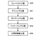
図1を参照して、ウェハ10上には、図示しないが微小構造体を有する複数のチップが形成されているものとする。そして、テスタ1に搬送されてウェハテストが実行される。そして、次にダイシング部50に搬送されてダイシング工程が実行される。具体的には、ウェハ上に形成された複数のチップがダイシングソーによりチップ毎にカッティングされる。そして、ボンダー60に搬送される。ボンダー60において、各チップ毎に基板側のリード電極とチップに形成されているボンディングパッドとを接続するボンディング工程が実行される。
Referring to FIG. 1, it is assumed that a plurality of chips having a microstructure are formed on
そして、図示しないが後の工程においてチップの封入あるいは封止工程(パッケージング工程とも称する)が実行される。なお、後述するが、テスタ1でのウェハテスト結果であるテスト情報がボンダー60に伝達される。
Although not shown, a chip encapsulation or sealing process (also referred to as a packaging process) is performed in a later process. As will be described later, test information which is a wafer test result in the
図2は、図1の処理の流れを説明するフロー図である。
図2に示されるように上述したテスタ1によりウェハテスト工程が実行される(ステップSP0)。次に、ダイシング50によってダイシング工程(ステップSP1)が実行される。そして次にボンダー60によりワイヤボンディング等のボンディング工程が実行される(ステップSP2)。そしてボンディングが実行された後、パッケージング工程が行なわれる(ステップSP3)。そして、パッケージング工程後、出荷前の完成品をテストする出荷前検査工程が実行される(ステップSP4)。
FIG. 2 is a flowchart illustrating the processing flow of FIG.
As shown in FIG. 2, the wafer test process is executed by the
本例においては、テスタ1におけるウェハテストのテスト結果に基づいて、製造段階でのデバイスのばらつきを補正する方式について説明する。具体的には、ウェハテスト時に検出されたテスト結果から当該テスト結果に対応する補正情報を参照して、デバイスの出力電圧を調整する方式について説明する。
In this example, a method for correcting device variations in the manufacturing stage based on the test result of the wafer test in the
まず、本発明の実施の形態1に従うテスタ1について説明する。
図3は、本発明の実施の形態1に従う微小構造体のテスタ1を説明する概略構成図である。
First,
FIG. 3 is a schematic configuration diagram for explaining the
図3を参照して、ここでは本発明の実施の形態1に従うテスタ(検査装置)1と、微小な可動部を有する微小構造体のセンサチップTP(以下、単にチップとも称する)が複数形成された基板(ウェハ)10とが示されている。 Referring to FIG. 3, here, a plurality of testers (inspection apparatus) 1 according to the first embodiment of the present invention and a microstructure sensor chip TP (hereinafter also simply referred to as a chip) having a minute movable part are formed. A substrate (wafer) 10 is shown.
本例においてはテストする微小構造体の一例として、多軸である3軸加速度センサを挙げて説明する。 In this example, a multi-axis triaxial acceleration sensor will be described as an example of a microstructure to be tested.
テスタ1は、疎密波である音波を出力するスピーカ2と、外部とテスタ内部との間で入出力データの授受を実行するための入出力インタフェース15と、テスタ1全体を制御する制御部20と、テスト対象物との接触に用いられるプローブ針4と、プローブ針4を介してテスト対象物の特性評価となる測定値を検出するための測定部25と、制御部20からの指示に応答してスピーカ2を制御するスピーカ制御部30と、外部の音を検出するマイクロフォン(マイク)3と、マイク3が検出した音波を電圧信号に変換し、さらに増幅して制御部20に出力するための信号調整部35と、各種プログラムおよびテスト対象物の特性評価となる情報を格納している記憶部40とを備える。なお、マイク3は、テスト対象物近傍に配置することが可能である。
The
本発明の実施の形態1に従うテスタの検査について説明する前にまずテスト対象物である微小構造体の3軸加速度センサについて説明する。なお、ここでは、センサの検出電圧を出力するセンサ部についてのみ説明し、後のセンサから検出された検出電圧を増幅する増幅部については後述する。 Before describing the tester inspection according to the first embodiment of the present invention, first, a microstructure triaxial acceleration sensor as a test object will be described. Here, only the sensor unit that outputs the detection voltage of the sensor will be described, and the amplification unit that amplifies the detection voltage detected from the subsequent sensor will be described later.
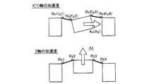
図4は、3軸加速度センサのデバイス上面から見た図である。
図4に示されるように、基板10に形成されるチップTPには、複数の電極パッドPDがその周辺に配置されている。そして、電気信号を電極パッドに対して伝達あるいは電極パッドから伝達するために金属配線が設けられている。そして、中央部には、クローバ型を形成する4つの重錐体ARが配置されている。
FIG. 4 is a view of the triaxial acceleration sensor as viewed from the top surface of the device.
As shown in FIG. 4, the chip TP formed on the
図5は、3軸加速度センサの概略図である。
図5を参照して、この3軸加速度センサはピエゾ抵抗型であり検出素子であるピエゾ抵抗素子が拡散抵抗として設けられている。このピエゾ抵抗型の加速度センサは、安価なICプロセスを利用することができるとともに、検出素子である抵抗素子を小さく形成しても感度低下がないため、小型化・低コスト化に有利である。
FIG. 5 is a schematic diagram of a three-axis acceleration sensor.
Referring to FIG. 5, the three-axis acceleration sensor is a piezoresistive type, and a piezoresistive element as a detection element is provided as a diffused resistor. This piezoresistive acceleration sensor can use an inexpensive IC process and is advantageous in miniaturization and cost reduction because the sensitivity does not decrease even if the resistance element as a detection element is formed small.
具体的な構成としては、中央の重錐体ARは4本のビームBMで支持した構造となっている。ビームBMはX,Yの2軸方向で互いに直交するように形成されており、1軸当りに4つのピエゾ抵抗素子を備えている。Z軸方向検出用の4つのピエゾ抵抗素子は、X軸方向検出用ピエゾ抵抗素子の横に配置されている。重錐体ARの上面形状はクローバ型を形成し、中央部でビームBMと連結されている。このクローバ型構造を採用することにより、重錐体ARを大きくすると同時にビーム長も長くすることができるため小型であっても高感度な加速度センサを実現することが可能である。 As a specific configuration, the central heavy cone AR is supported by four beams BM. The beam BM is formed so as to be orthogonal to each other in the X-axis and Y-axis directions, and includes four piezoresistive elements per axis. Four piezoresistive elements for detecting the Z-axis direction are arranged beside the piezoresistive elements for detecting the X-axis direction. The top surface shape of the heavy cone AR forms a crowbar shape and is connected to the beam BM at the center. By adopting this crowbar type structure, the heavy cone AR can be enlarged and the beam length can be increased at the same time, so that a highly sensitive acceleration sensor can be realized even if it is small.
このピエゾ抵抗型の3軸加速度センサの動作原理は、重錐体が加速度(慣性力)を受けると、ビームBMが変形し、その表面に形成されたピエゾ抵抗素子の抵抗値の変化により加速度を検出するメカニズムである。そしてこのセンサ出力は、3軸それぞれ独立に組込まれた後述するホイートストンブリッジの出力から取り出す構成に設定されている。 The principle of operation of this piezoresistive three-axis acceleration sensor is that when the heavy cone receives acceleration (inertial force), the beam BM is deformed and acceleration is caused by a change in the resistance value of the piezoresistive element formed on the surface. It is a mechanism to detect. And this sensor output is set to the structure taken out from the output of the Wheatstone bridge mentioned later incorporated in each 3 axis | shaft independently.
図6は、各軸方向の加速度を受けた場合の重錐体とビームの変形を説明する概念図である。 FIG. 6 is a conceptual diagram for explaining the deformation of the heavy cone and the beam when the acceleration in each axial direction is received.
図6に示されるようにピエゾ抵抗素子は、加えられた歪みによってその抵抗値が変化する性質(ピエゾ抵抗効果)を持っており、引張歪みの場合は抵抗値が増加し、圧縮歪みの場合は抵抗値が減少する。本例においては、X軸方向検出用ピエゾ抵抗素子Rx1〜Rx4、Y軸方向検出用ピエゾ抵抗素子Ry1〜Ry4およびZ軸方向検出用ピエゾ抵抗素子Rz1〜Rz4が一例として示されている。 As shown in FIG. 6, the piezoresistive element has a property that its resistance value changes due to applied strain (piezoresistive effect). In the case of tensile strain, the resistance value increases, and in the case of compressive strain, The resistance value decreases. In this example, X-axis direction detecting piezoresistive elements Rx1 to Rx4, Y-axis direction detecting piezoresistive elements Ry1 to Ry4, and Z-axis direction detecting piezoresistive elements Rz1 to Rz4 are shown as examples.
図7は、各軸に対して設けられるホイートストンブリッジの回路構成図である。
図7(a)は、X(Y)軸におけるホイートストンブリッジの回路構成図である。X軸およびY軸の出力電圧としてはそれぞれVxoutおよびVyoutとする。
FIG. 7 is a circuit configuration diagram of a Wheatstone bridge provided for each axis.
FIG. 7A is a circuit configuration diagram of the Wheatstone bridge in the X (Y) axis. The output voltages of the X axis and the Y axis are Vxout and Vyout, respectively.
図7(b)は、Z軸におけるホイートストンブリッジの回路構成図である。Z軸の出力電圧としてはVzoutとする。 FIG. 7B is a circuit configuration diagram of the Wheatstone bridge in the Z axis. The output voltage of the Z axis is Vzout.
上述したように加えられた歪みによって各軸4つのピエゾ抵抗素子の抵抗値は変化し、この変化に基づいて各ピエゾ抵抗素子は例えばX軸Y軸においては、ホイートストンブリッジで形成される回路の出力各軸の加速度成分が独立に分離された出力電圧として検出される。なお、上記の回路が構成されるように図4で示されるような上述した金属配線等が連結され、所定の電極パッドから各軸に対する出力電圧が検出されるように構成されている。 As described above, the resistance values of the four piezoresistive elements on each axis change due to the applied strain. Based on this change, each piezoresistive element outputs, for example, an output of a circuit formed by a Wheatstone bridge on the X axis and Y axis. The acceleration component of each axis is detected as an independently separated output voltage. It is to be noted that the above-described metal wiring as shown in FIG. 4 is connected so that the above circuit is configured, and the output voltage for each axis is detected from a predetermined electrode pad.
また、この3軸加速度センサは、加速度のDC成分も検出することができるため重力加速度を検出する傾斜角センサとしても用いることが可能である。 In addition, since this triaxial acceleration sensor can detect the DC component of acceleration, it can also be used as an inclination angle sensor for detecting gravitational acceleration.
図8は、3軸加速度センサの傾斜角に対する出力応答を説明する図である。
図8に示されるようにセンサをX,Y,Z軸周りに回転させX,Y,Z軸それぞれのブリッジ出力をデジタルボルトメータで測定したものである。センサの電源としては低電圧電源+5Vを使用している。なお、図8に示される各測定点は、各軸出力のゼロ点オフセットを算術的に減じた値がプロットされている。
FIG. 8 is a diagram for explaining the output response to the tilt angle of the triaxial acceleration sensor.
As shown in FIG. 8, the sensor is rotated around the X, Y, and Z axes, and the bridge output of each of the X, Y, and Z axes is measured with a digital voltmeter. As a power source for the sensor, a low voltage power source + 5V is used. Each measurement point shown in FIG. 8 is plotted with a value obtained by arithmetically subtracting the zero point offset of each axis output.
図9は、重力加速度(入力)とセンサ出力との関係を説明する図である。
図9に示される入出力関係は、図8の傾斜角の余弦からX,Y,Z軸にそれぞれ関わっている重力加速度成分を計算し、重力加速度(入力)とセンサ出力との関係を求めてその入出力の線形性を評価したものである。すなわち加速度と出力電圧との関係はほぼ線形である。
FIG. 9 is a diagram for explaining the relationship between gravitational acceleration (input) and sensor output.
The input / output relationship shown in FIG. 9 is obtained by calculating the gravitational acceleration components related to the X, Y, and Z axes from the cosine of the inclination angle of FIG. The linearity of the input / output is evaluated. That is, the relationship between acceleration and output voltage is almost linear.
図10は、3軸加速度センサの周波数特性を説明する図である。
図10に示されるようにX,Y,Z軸それぞれのセンサ出力の周波数特性は、一例として3軸ともに200Hz付近まではフラットな周波数特性を示しておりX軸においては602Hz、Y軸においては600Hz、Z軸においては883Hzにおいて共振している。
FIG. 10 is a diagram for explaining the frequency characteristics of the three-axis acceleration sensor.
As shown in FIG. 10, the frequency characteristics of the sensor output for each of the X, Y, and Z axes are flat frequency characteristics up to about 200 Hz for all three axes, for example, 602 Hz for the X axis and 600 Hz for the Y axis. The Z axis resonates at 883 Hz.
再び図3を参照して、本発明の実施の形態1に従うテスタの検査は、微小構造体である3軸加速度センサに対して疎密波である音波を出力することによりその音波に基づく微小構造体の可動部の動きを検出してその特性を評価する方式である。 Referring to FIG. 3 again, the inspection of the tester according to the first embodiment of the present invention is performed by outputting a sound wave that is a sparse wave to the triaxial acceleration sensor that is a microstructure, and the microstructure based on the sound wave. This is a method of detecting the movement of the movable part and evaluating its characteristics.
図11のフローチャート図を用いて、本発明の実施の形態1に従う微小構造体の検査方式について説明する。 The microstructure inspection method according to the first embodiment of the present invention will be described with reference to the flowchart of FIG.
図11を参照して、まず微小構造体の検査(テスト)を開始(スタート)する(ステップS0)。次に、検出チップTPの電極パッドPDにプローブ針4を接触させる(ステップS1)。具体的には、図5で説明したホイートストンブリッジ回路の出力電圧を検出するために所定の電極パッドPDにプローブ針4を接触させる。なお、図1の構成においては、一組のプローブ針4を用いた構成が示されているが、複数組のプローブ針を用いた構成とすることも可能である。複数組のプローブ針を用いることにより並列に出力信号を検出することができる。
Referring to FIG. 11, the inspection (test) of the microstructure is first started (step S0). Next, the
次に、スピーカ2から出力するテスト音波を設定する(ステップS2a)。具体的には、制御部20は、入出力インタフェース15を介して外部からの入力データの入力を受ける。そして、制御部20は、スピーカ制御部30を制御し、入力データに基づいて所望の周波数および所望の音圧のテスト音波をスピーカ2から出力するようにスピーカ制御部30に対して指示する。次に、スピーカ2から検出チップTPに対してテスト音波を出力する(ステップS2b)。
Next, a test sound wave output from the
次に、マイク3を用いてスピーカ2から検出チップTPに対して与えられるテスト音波を検出する(ステップS3)。マイク3で検出したテスト音波は信号調整部35において、電圧信号に変換・増幅されて制御部20に出力される。
Next, a test sound wave applied from the
次に、制御部20は、信号調整部35から入力される電圧信号を解析し、判定して、所望のテスト音波が到達しているかどうかを判定する(ステップS4)。
Next, the
ステップS4において、制御部20は、所望のテスト音波であると判定した場合には、次のステップS5に進み、検出チップの特性値を測定する。具体的には、プローブ針4を介して伝達される電気信号に基づいて測定部25で特性値を測定する(ステップS5)。
In step S4, when it determines with it being a desired test sound wave, the
具体的には、スピーカ2から出力される疎密波であるテスト音波の到達すなわち空気振動により検出チップの微小構造体の可動部は動く。この動きに基づいて変化する微小構造体である3軸加速度センサの抵抗値の変化についてプローブ針4を介して電気的な検出信号である出力電圧を測定することが可能である。
Specifically, the movable part of the microstructure of the detection chip is moved by the arrival of the test sound wave that is a dense wave output from the
一方、ステップS4において、所望のテスト音波でないと判定した場合には、再びステップS2に戻りテスト音波を再設定する。その際、制御部20は、スピーカ制御部30に対してテスト音波の補正をするようにスピーカ制御部30に対して指示する。スピーカ制御部30は、制御部20からの指示に応答して所望のテスト音波となるように周波数および/または音圧を微調整してスピーカ2から所望のテスト音波を出力するように制御する。なお、本例においては、テスト音波を検出して、所望のテスト音波に補正する方式について説明しているが、予め所望のテスト音波が検出チップの微小構造体に到達する場合には、特にテスト音波の補正手段およびテスト音波を補正する方式を設けない構成とすることも可能である。具体的には、予めステップS2a〜S4に至る処理をテスト開始前に実行し、スピーカ制御部30において、所望のテスト音波を出力するための補正された制御値を記憶する。そして、実際の微小構造体のテスト時には、スピーカ制御部30は、この記録された制御値でスピーカ2への入力を制御することにより、上述したテスト時におけるステップS3およびS4の処理を省略することも可能である。
On the other hand, if it is determined in step S4 that it is not the desired test sound wave, the process returns to step S2 again to reset the test sound wave. At that time, the
次に、制御部20は、測定された特性値すなわち測定データが、許容範囲であるかどうかを判定する(ステップS6)。ステップS6において、許容範囲であると判定された場合には合格(ステップS7)であるとし、データの出力および保存を実行する(ステップS8)。そして、ステップS9に進む。本発明の実施の形態1においては、制御部20において、許容範囲の判定としてスピーカ2から出力されるテスト音波の入力により、3軸加速度センサの周波数応答特性を検出して、そのチップが適正な特性を有しているかどうかを判定する。なお、データの保存については、制御部20からの指示に基づいてテスタ1内部に設けられた記憶部40に記憶されるものとする。また、記憶部40には、許容範囲に関する情報とともに、許容範囲に含まれるチップについて、測定データに基づいてデバイスの特性を評価あるいは判定するテスト情報も記憶されているものとする。なお、このテスト情報には、後述するが例えば後段の回路である増幅部の特性値を調整するための測定データに対応する補正情報も含まれるものとする。
Next, the
ステップS9において、次に検査するチップがない場合には、微小構造体の検査(テスト)を終了する(ステップS10)。 In step S9, when there is no chip to be inspected next, the inspection (test) of the microstructure is finished (step S10).
一方、ステップS9において、さらに次の検査すべきチップがある場合には、最初のステップS1に戻り再び上述した検査を実行する。 On the other hand, if there is a further chip to be inspected in step S9, the process returns to the first step S1 and the above-described inspection is executed again.
ここで、ステップS6において、制御部20は、測定された特性値すなわち測定データが、許容範囲ではないと判定した場合には不合格(ステップS11)であるとし、再検査する(ステップS12)。具体的には、再検査により、許容範囲外であると判定されるチップについては除去することができる。あるいは、許容範囲外であると判定されるチップであっても複数のグループに分けることができる。すなわち、厳しいテスト条件にクリアできないチップであっても補修・補正等行なうことにより実際上出荷しても問題もないチップも多数存在することが考えられる。したがって、再検査等によりそのグループ分けを実行することによりチップを選別し、選別結果に基づいて出荷することも可能である。
Here, in Step S6, when it is determined that the measured characteristic value, that is, measurement data is not within the allowable range, the
なお、本例においては、一例として3軸加速度センサの動きに応答して、3軸加速度センサに設けられたピエゾ抵抗素子の抵抗値の変化を出力電圧により検出し、判定する構成について説明したが特に抵抗素子に限られず容量素子やリアクタンス素子等のインピーダンス値の変化もしくはインピーダンス値の変化に基づく電圧、電流、周波数、位相差、遅延時間および位置等の変化を検出し、判定する構成とすることも可能である。 In this example, as an example, a configuration has been described in which a change in the resistance value of a piezoresistive element provided in the triaxial acceleration sensor is detected and determined in response to the movement of the triaxial acceleration sensor. In particular, it is not limited to resistance elements, and it is configured to detect and judge changes in impedance values such as capacitive elements and reactance elements, or changes in voltage, current, frequency, phase difference, delay time, position, etc. based on changes in impedance values. Is also possible.
図12は、スピーカ2から出力されたテスト音波に応答する3軸加速度センサの周波数応答を説明する図である。
FIG. 12 is a diagram for explaining the frequency response of the three-axis acceleration sensor that responds to the test sound wave output from the
図12においては、音圧として1Pa(パスカル)のテスト音波を与えて、その周波数を変化させた場合に3軸加速度センサから出力される出力電圧が示されている。縦軸が3軸加速度センサの出力電圧振幅(mV)、横軸がテスト音波の周波数(Hz)を示している。 FIG. 12 shows the output voltage output from the triaxial acceleration sensor when a test sound wave of 1 Pa (Pascal) is applied as the sound pressure and the frequency is changed. The vertical axis indicates the output voltage amplitude (mV) of the triaxial acceleration sensor, and the horizontal axis indicates the frequency (Hz) of the test sound wave.
ここでは、特にX軸方向に対して得られる出力電圧が示されている。本例においては、X軸のみしか図示していないが、同様にY軸およびZ軸においても同様の周波数特性を得ることが可能であるため3軸それぞれにおいて加速度センサの特性を評価することができる。 Here, an output voltage obtained particularly in the X-axis direction is shown. In this example, only the X axis is shown, but similarly, the same frequency characteristic can be obtained for the Y axis and the Z axis, so that the characteristics of the acceleration sensor can be evaluated for each of the three axes. .
次に、上述した本発明の実施の形態1に従うテスト音波に従うウェハテストを実行した場合に、許容範囲であると判定されたチップに対して、測定データに基づいてデバイスの特性を評価あるいは判定する方式について説明する。 Next, when the wafer test according to the test sound wave according to the first embodiment of the present invention described above is executed, the characteristics of the device are evaluated or determined based on the measurement data for the chip determined to be within the allowable range. The method will be described.
ここでは、一例として、デバイスのセンサ感度のばらつきの判定について説明する。
図13は、本発明の実施の形態1に従うテスタ1の検査結果に基づいてデバイスのセンサ感度のばらつきの判定を説明する図である。
Here, as an example, determination of variation in sensor sensitivity of a device will be described.
FIG. 13 is a diagram illustrating determination of variation in sensor sensitivity of a device based on the test result of the
ここでは、テスタ1のテスト音波に従って検出される検出電圧の基準値をS0(理想的な検出電圧値)とした場合において、実際のデバイスから検出された検出電圧rに従って分類分けする方式が示されている。具体的には、0.5S0〜1.5S0の範囲において0.1S0毎にグループ分けされている。たとえば、r<0.5S0の場合には、グループ1とする。また、0.5S0≦r<0.6S0の場合には、グループ2とする。同様の方式に従って、1.4S0≦r<1.5S0の場合にはグループ11とする。そして、r≧1.5S0の場合には、グループ12とする。これらの情報は、テスタ1の記憶部40に格納されており、制御部20の指示のもと読み出されて分類判断が実行されるものとする。
Here, a method of classifying according to the detected voltage r detected from the actual device when the reference value of the detected voltage detected according to the test sound wave of the
そして、この分類判断に基づいて、後述する増幅部の特性値、具体的には、増幅率を調整する。 And based on this classification judgment, the characteristic value of the amplification part mentioned later, specifically, an amplification factor is adjusted.
ここでは、0.9S0≦r<1.0S0の場合におけるグループ6の増幅率10倍(×10)を基準としてこの増幅値A0(=10S0)のほぼ±10%の範囲内に各グループに対応する検出電圧が増幅されるように調整する。
Here, each group corresponds to an amplification value A0 (= 10S0) within a range of approximately ± 10% with reference to the
たとえば、グループ2の場合には、増幅率18倍(×18)に設定される。また、グループ3の場合には、増幅率15倍(×15)に設定される。また、グループ11の場合には、増幅率7倍(×7)に設定される。このようにデバイスから検出される検出電圧のばらつきに対応して増幅器の増幅率を調整することにより各デバイスにおけるセンサ感度の補正が可能となる。
For example, in the case of
なお、グループ1あるいはグループ12の場合には検出電圧が小さすぎるあるいは大きすぎるすなわちセンサ感度が低すぎるあるいは高すぎるためセンサに適さないすなわち許容範囲外として不合格としている。
In the case of
そして、本例においては、このテスタ1でのテスト結果がテスト結果情報としてボンダー60に出力される。具体的には、例えば増幅部の特性値を調整するための補正情報としてセンサ感度を調整するの増幅率に関する調整データが出力される。
In this example, the test result in the
図14は、本発明の実施の形態1に従う加速度センサの増幅部を説明する図である。
図14を参照して、ここでは、図7で説明したホイートストンブリッジの回路構成で示される本発明の実施の形態1に従うセンサ部SNとセンサ部SNの出力結果を増幅する増幅部とが示されている。
FIG. 14 is a diagram illustrating an amplifying unit of the acceleration sensor according to the first embodiment of the present invention.
Referring to FIG. 14, here, sensor unit SN according to the first embodiment of the present invention shown in the circuit configuration of the Wheatstone bridge described in FIG. 7 and an amplification unit that amplifies the output result of sensor unit SN are shown. ing.
センサ部SNについては、図7で説明したように各軸(X,Y,Z)についてホイートストンブリッジが形成されてセンサ部SNから可動部の動きに従って出力電圧が検出される。たとえば、ここでは、1軸について検出された出力電圧を増幅する場合が示されている。 As for sensor unit SN, as described with reference to FIG. 7, a Wheatstone bridge is formed for each axis (X, Y, Z), and an output voltage is detected from sensor unit SN according to the movement of the movable unit. For example, here, a case where the output voltage detected for one axis is amplified is shown.
増幅部は、直列に接続された多段構成の複数の増幅器で構成される。具体的には、本例においては2段構成の増幅器100,300が示される。また、増幅部は、増幅器100に対してオフセット電圧を調整するオフセット電圧調整部200をさらに含む。なお、本例においては、一例として増幅器100の増幅率を調整する場合について説明する。ここで、増幅器100は、いわゆるインスツルメンテーション・アンプである。
The amplifying unit includes a plurality of multi-stage amplifiers connected in series. Specifically, in this example, two-
増幅器100は、コンパレータ110〜112と、抵抗素子101〜106と、抵抗調整部120とを含む。なお、コンパレータ110および111は、非反転増幅段を構成し、コンパレータ112は、差像増幅段を構成する。
The
コンパレータ110は、ノードN0とノードN1とに伝達された入力電圧を比較して、その結果をノードN2に伝達する。抵抗素子103は、ノードN2とノードN1との間に電気的に結合される。抵抗調整部120は、ノードN1とノードN5との間に電気的に結合される。抵抗素子104は、ノードN5とノードN7との間に電気的に結合される。コンパレータ111は、ノードN5とノードN6とに伝達された入力電圧を比較して、その結果をノードN7に伝達する。抵抗素子101は、ノードN2とノードN3との間に電気的に結合される。抵抗素子105は、ノードN7とノードN8との間に電気的に結合される。コンパレータ112は、ノードN3とノードN8とに伝達された入力電圧を比較して、その結果をノードN4に伝達する。抵抗素子102は、ノードN3とノードN4との間に電気的に結合される。抵抗素子106は、ノードN8とノードN9との間に電気的に結合される。
抵抗調整部120は、抵抗値の調整が可能であり、この抵抗値の調整に基づいてコンパレータ110および111のゲイン(増幅率)が調整される。具体的には、基準となる基準抵抗値から抵抗値を高くすればするほど、ノードN1およびN5にかかる負荷が上昇するためゲイン(増幅率)が下がり、逆に基準となる基準抵抗値から抵抗値を低くすればするほどノードN1およびN5にかかる負荷が下降するためゲイン(増幅率)が上がることとなる。
The
オフセット電圧調整部200は、コンパレータ210と電圧調整部220とを含む。
コンパレータ210は、ノードN10とノードN11とに伝達された入力電圧を比較して、その結果をノードN9に伝達する。なお、このコンパレータ210は、出力ノードN9と入力ノード10とが電気的に結合されたいわゆるボルテージフォロワであり、ノードN11に伝達された電圧に追従して同一の電圧がノードN9に伝達される。
Offset
電圧調整部220は、後述するが電源電圧Vddと接地電圧GNDとの間に設けられた抵抗素子により抵抗分割されており、ノードN11と接続する抵抗素子の接続位置により抵抗分割に伴う電圧の調整が可能である。
As will be described later,
オフセット電圧の調整は、この電圧調整部220における抵抗素子の接続位置を調整することにより調整される。
The offset voltage is adjusted by adjusting the connection position of the resistance element in the
増幅器300は、増幅器100の増幅出力信号と、所定の基準電圧信号Vrefとの入力を受けて設定されたの増幅率で増幅出力信号をさらに増幅して出力する。ここでは、簡略して記載しているが、増幅器300についても増幅器100と同様の構成であり、抵抗調整部の抵抗値を調整することにより増幅率を調整可能であるものとする。なお、オフセット電圧を調整するオフセット電圧調整部200は、初段の増幅器100に対して設けられているが、後段の増幅器300に対して設けることも可能である。
The
一般的に多段構成の増幅器の場合には、各段の増幅器それぞれについて独立に調整可能であり、ここでは、前段部の増幅器100の調整について説明しているが、これに限られずたとえば後段の増幅器300の増幅率を調整することも可能である。
In general, in the case of an amplifier having a multi-stage configuration, each amplifier in each stage can be adjusted independently. Here, the adjustment of the
図15は、本発明の実施の形態1に従う増幅率の調整について説明する図である。
本発明の実施の形態1においては、一例として上述したボンダー60がテスタ1のテスト結果情報の入力を受けて、それに基づいてワイヤボンディングを実行する場合について説明する。本例においては、本発明の実施の形態1に従うテスト音波に従うテスト検査結果に含まれる補正データに基づいて製造段階でのセンサ感度のばらつきを補償する方式について説明する。
FIG. 15 is a diagram illustrating adjustment of the amplification factor according to the first embodiment of the present invention.
In the first embodiment of the present invention, as an example, a case will be described in which the
図15を参照して、ここでは、半導体基板1000上にセンサチップTPと、増幅部を構成する2つの増幅チップAMTP,AMTP#とが載置される。そして、ボンダー60において、各チップ間の配線接続が実行される。ここでは、主に、センサチップTPと、増幅チップAMTPとの接続について説明する。
Referring to FIG. 15, here, a sensor chip TP and two amplification chips AMTP and ANTP # constituting an amplification unit are mounted on a
本発明の実施の形態1に従うチップTPにおいてはセンサ部SNの周辺のパッド領域において複数の抵抗素子が設けられている。そして、複数のパッド間にそれぞれ複数の抵抗素子の各々が電気的に結合された状態となっている。 In chip TP according to the first embodiment of the present invention, a plurality of resistance elements are provided in a pad region around sensor portion SN. Each of the plurality of resistance elements is electrically coupled between the plurality of pads.
本例においては、チップTPにおいて抵抗調整部120を構成する複数の抵抗素子と、電圧調整部220を構成する複数の抵抗素子とがそれぞれ設けられている。抵抗調整部120は、抵抗素子Ra0〜RaN−1を含み、各抵抗素子がそれぞれパッドPDa0〜PDaNの間にそれぞれ設けられている。電圧調整部220は、複数の抵抗素子Rb0〜RbM−1を含み、各抵抗素子がそれぞれパッドPDb0〜PDbMの間にそれぞれ設けられている。
In this example, in the chip TP, a plurality of resistance elements constituting the
そして、ワイヤボンディングによりノードN1とノードN5とそれぞれ電気的に結合される2つのパッドPDaが複数のパッドの中から選択される。これにより、ノードN1とノード5との間の抵抗値が調整される。たとえば、本例においてはノードN1とパッドPDa0とが電気的に結合される。また、ノードN5とパッドPDa2とが電気的に結合される。これにより、抵抗Ra0,Ra1がノードN1とノードN5との間に直列に接続された状態となる。
Then, two pads PDa that are respectively electrically coupled to the node N1 and the node N5 are selected from a plurality of pads by wire bonding. Thereby, the resistance value between the node N1 and the
したがって、このようなワイヤボンディングにより、複数のパッドPDaの中から2つのパッドPDaを選択して、電気的に結合させることによりノードN1とノードN5との間に接続される抵抗素子数を調整することが可能となり、その間の抵抗素子の抵抗値を調整することができる。これにより、上述したように例えば基準となる基準抵抗値から抵抗値を調整することにより増幅率を調整して、増幅後の出力信号の値を調整することができる。 Therefore, by such wire bonding, two pads PDa are selected from the plurality of pads PDa and electrically coupled to adjust the number of resistance elements connected between the nodes N1 and N5. And the resistance value of the resistance element in the meantime can be adjusted. As a result, as described above, for example, the amplification factor can be adjusted by adjusting the resistance value from the reference resistance value serving as a reference, and the value of the output signal after amplification can be adjusted.
ボンダー60は、ワイヤボンディングに際し、上記のテスト結果情報の入力を受けて、増幅器100の増幅率を調整するためにテスタ1でのグループ分けに従って対応するグループの増幅率となるように接続関係を決定し、複数のパッドPDaの中からボンディングするパッドを選択する。なお、図示しないが、ボンダー60内においては、テスタ1からのテスト結果情報の入力を受けて増幅率を調整するためにボンディング位置を調整するための調整プログラムおよび各種制御プログラムを格納する記憶部を有しているものとする。これにより、ROMに補正値を記録して補正する方式やレーザートリミングによって抵抗体の抵抗値を変えて補正する方式に比べて非常に安価に調整することが可能となる。
The
また、本方式を採用することにより、パッケージング前に調整が行なわれるためパッケージング後の出荷前検査工程において、当該検査時に出力が飽和しないように設定することができるため出荷前検査時の検査時間や補正時間が短くなる。 In addition, by adopting this method, adjustments are made before packaging, so in the pre-shipment inspection process after packaging, it can be set so that the output does not saturate at the time of the inspection. Time and correction time are shortened.
また、上述したように電圧調整部220を構成する複数の抵抗素子Rb0〜RbM−1もチップTP上に構成され、パッドPDb0〜PDbMの間にそれぞれ設けられている。ここで、パッドPDb0は、電源電圧Vddと電気的に結合される。また、パッドPDbMは、接地電圧GNDと電気的に結合される。したがって、複数の抵抗素子が電源電圧Vddと接地電圧GNDとの間に直列に接続された構成であり抵抗分割により、各パッドPDbから出力される電圧値を調整することが可能となる。したがって、ノードN11と接続されるパッドPDbの位置を変えることにより抵抗分割に従う所望の電圧値がコンパレータ210の入力ノードに供給される。上述したようにコンパレータ210はボルテージフォロワであるためこの抵抗分割に従う所望の電圧値がノードN9に伝達されてオフセット電圧値として増幅器100に出力される。これにより、簡易な方式により増幅器100の特性値に含まれるオフセット電圧値を調整することが可能である。本例においては、例えば電源電圧Vddが5Vである場合に、2.5Vを基準となるオフセット電圧値(以下、オフセット基準値とも称する)として設定する。
Further, as described above, the plurality of resistance elements Rb0 to RbM-1 configuring the
図16は、本発明の実施の形態1に従うオフセット電圧補正値の分類について説明する図である。 FIG. 16 is a diagram illustrating the classification of offset voltage correction values according to the first embodiment of the present invention.
ここでは、オフセット電圧補正値がグループ1〜グループ42に細分化されて、それらに基づいて増幅器のオフセット電圧補正値(調整値)が決定されている。ここでは、オフセット基準値を基準に−20mV〜20mVの範囲内において1mV毎に分類分けされた場合が示されている。そして、オフセット電圧補正値としては、オフセットのために検出された検出電圧に補正値としてオフセット電圧補正値を乗せた値がオフセット基準値に対してほぼ−0.5mV〜0.5mVの範囲内に収まるように決定されている。これにより、オフセットをほぼキャンセルして精度の高い増幅器における増幅が可能となる。
Here, the offset voltage correction value is subdivided into
たとえば、検出電圧qについて、q<−20mVの場合をグループ1とする。そして、−20mV≦q<−19mVの場合をグループ2とする。同様の方式に従って、19mV≦q<20mVの場合をグループ41とする。さらにq≧20mVの場合をグループ42とする。そして、このグループ分けに従ってオフセット電圧が決定される。たとえば、グループ2に対応する場合には、オフセット電圧補正値は+19.5mVとされる。また、グループ3の場合には、オフセット電圧補正値は+18.5Vとされる。なお、グループ1あるいはグループ42の場合には、オフセット電圧補正値が正負において過大となりすぎるため不良判定としている。これらの情報は、テスタ1の記憶部40に格納されており、制御部20の指示のもと読み出されて分類判断が実行されるものとする。
For example, regarding the detection voltage q, the case of q <−20 mV is set as
本発明の実施の形態1においては、テスタ1において、検出電圧qを算出して、上記の分類結果に基づき決定されるオフセット電圧補正値を決定し、そのテスト結果情報をボンダー60に出力する。ボンダー60は、オフセット電圧補正値を受けて、ワイヤボンディングにより所望のオフセット電圧となるように電圧調整部220で所定のパッドPDbとノードN11とを電気的に結合する。なお、検出電圧qは、チップTPから出力される出力基準値からオフセット基準値を差分した値に相当する。
In the first embodiment of the present invention, the
ここで、チップTPの出力基準値について説明する。
図17は、チップTPからの出力結果を説明する図である。
Here, the output reference value of the chip TP will be described.
FIG. 17 is a diagram for explaining an output result from the chip TP.
上記のテスタ1において、テスト音波をデバイスに入力するとプローブ針を介して出力電圧が検出される。
In the
図17に示される波形は、ある測定区間において所定のサンプリング期間において測定した出力電圧をプロットして、検出された出力電圧の波形図である。 The waveform shown in FIG. 17 is a waveform diagram of the output voltage detected by plotting the output voltage measured in a predetermined sampling period in a certain measurement section.
ここで示されるようにチップTPからの出力結果は、基準となる出力基準値を中心に振幅する電圧信号波形となる。したがって、ある測定区間における平均値を求めることにより基準となる出力基準値を容易に測定することが可能となる。 As shown here, the output result from the chip TP is a voltage signal waveform that swings around an output reference value serving as a reference. Therefore, it is possible to easily measure the output reference value as a reference by obtaining an average value in a certain measurement section.
なお、上述のセンサ感度の検査においては、一例としてある測定区間における最大の出力電圧を検出電圧として用いることとする。 In the above-described sensor sensitivity inspection, as an example, the maximum output voltage in a certain measurement section is used as the detection voltage.
したがって、本発明の実施の形態1に従うテスト方式により、センサ感度およびオフセット電圧について別々に特性検査を実行する必要がなく、1回のテストに従う測定データから簡易かつ高速に増幅器の特性値である増幅率およびオフセット電圧について並列に調整することが可能になる。 Therefore, according to the test method according to the first embodiment of the present invention, it is not necessary to separately perform the characteristic inspection for the sensor sensitivity and the offset voltage, and amplification that is the characteristic value of the amplifier simply and at high speed from the measurement data according to one test. The rate and offset voltage can be adjusted in parallel.
なお、上記で説明した本発明の実施の形態1に従うセンサ感度およびオフセット電圧補正値の少なくとも一方の分類方法についてコンピュータに実行させるプログラムを予めFD、CD−ROMあるいはハードディスク等の記憶媒体に記憶させておくことも可能である。 Note that a program that causes a computer to execute the classification method of at least one of the sensor sensitivity and the offset voltage correction value according to the first embodiment of the present invention described above is stored in advance in a storage medium such as an FD, a CD-ROM, or a hard disk. It is also possible to leave.
この場合には、テスタ1に記録媒体に格納された当該プログラムを読み取るドライバ装置を設けて、ドライバ装置を介してテスタ1内の制御部20がプログラムを受信して、上述した許容範囲の判定を実行することも可能である。さらに、ネットワーク接続されている場合には、サーバから当該プログラムをダウンロードすることも可能である。
In this case, the
(実施の形態2)
上記の実施の形態1においては、ボンダー60において、テスタ1でのテスト結果情報に基づいてワイヤボンディングによりセンサの特性を調整する方式について主に説明したが、本発明の実施の形態2においては、さらに別の方式に従ってセンサの特性を調整する方式について説明する。
(Embodiment 2)
In the above-described first embodiment, the method of adjusting the sensor characteristics by wire bonding based on the test result information in the
図18は、本発明の実施の形態2に従う加速度センサの増幅部およびその増幅率の調整を説明する図である。 FIG. 18 is a diagram illustrating the amplification unit of the acceleration sensor according to the second embodiment of the present invention and the adjustment of the amplification factor.
図18を参照して、本発明の実施の形態2に従う加速度センサの増幅部は、いわゆるプログラマブルアンプ(PGA)で構成される。 Referring to FIG. 18, the amplifying unit of the acceleration sensor according to the second embodiment of the present invention is configured by a so-called programmable amplifier (PGA).
具体的には、上述したセンサ部SNで構成されるセンサチップTP#と、プログラマブルアンプ400および記憶部450で構成される増幅チップAPTPとが半導体基板1001上に載置されて、各チップ間の配線接続が実行される。なお、本例においては、一例として記憶部450は、不揮発的なデータ記憶が可能なフラッシュメモリであるEEPROMで構成したものが示されているがこれに限られず、他のメモリを用いることも可能である。
Specifically, the sensor chip TP # configured by the sensor unit SN described above and the amplification chip APTP configured by the
プログラムアンプ400は、記憶部450に記憶されたデータに基づいてアンプの特性を調整することが可能である。
The
本発明の実施の形態2において、センサの特性を調整する方式について説明する。
本発明の実施の形態2においては、実施の形態1で説明したのと同様の方式に従ってテスタ1においてウェハテストを実行する。そして、テスタ1のテスト結果情報をROMデータ書き込み装置45に出力する。
In the second embodiment of the present invention, a method for adjusting the characteristics of the sensor will be described.
In the second embodiment of the present invention, a wafer test is performed in the
ROMデータ書き込み装置45は、テスタ1からのテスト結果情報に基づいて、図示しないROMインタフェース(I/F)を介して記憶部450にアンプの特性を決定するデータを書き込む。
Based on the test result information from the
これにより、例えば記憶部450にアンプの特性に含まれる増幅率を調整する増幅率調整データを書き込むことによりプログラムアンプ400の増幅率が調整されて、増幅後の出力信号の値を調整することができる。これに伴い、パッケージング前に調整が行なわれるためパッケージング後の出荷前検査工程において、当該検査時に出力が飽和しないように設定することができるため出荷前検査時の検査時間や補正時間が短くなる。
Thereby, for example, the amplification factor adjustment data for adjusting the amplification factor included in the characteristics of the amplifier is written in the
なお、ここでは、アンプの特性として、増幅率を調整するための増幅率調整データについて、ROMデータ書き込み装置45を用いて記憶部450に書き込む場合について説明したが、増幅率調整データに限られず、たとえば、実施の形態1で説明した方式に従ってオフセット補正値を算出し、テスト結果情報としてROMデータ書き込み装置45に与えることにより、オフセット調整データを記憶部450に書き込んでアンプの特性に含まれるオフセット電圧を調整することも可能である。
Here, as a characteristic of the amplifier, the case where the gain adjustment data for adjusting the gain is written in the
ここで、本発明の実施の形態2に従う増幅部は、プログラマブルアンプであるため実施の形態1においてボンダーのワイヤボンディングにしたがって増幅率の調整を実行する必要はないためパッケージ工程後においても簡易にその調整が可能であり、以下においては、パッケージ後の出荷前検査工程に再調整を実行する場合について説明する。 Here, since the amplification unit according to the second embodiment of the present invention is a programmable amplifier, it is not necessary to adjust the amplification factor according to the wire bonding of the bonder in the first embodiment. In the following description, a case where readjustment is performed in the pre-shipment inspection process after packaging will be described.
図19は、本発明の実施の形態2に従う増幅部の特性の調整の処理の流れを説明する図である。 FIG. 19 is a diagram illustrating a process flow for adjusting the characteristics of the amplification unit according to the second embodiment of the present invention.
図19を参照して、ここでは、パッケージング前とパッケージング後において、それぞれテスタのテスト結果情報を用いて調整する方式が示されている。 Referring to FIG. 19, here, a method of adjusting using test result information of a tester before and after packaging is shown.
パッケージング前において、ここでは、図18で説明したのと同様の構成が示されている。ここで示されているようにテスタ1でのテスト結果情報がROMデータ書き込み装置45に入力されて、ROMデータ書き込み装置45は、記憶部450に粗調整データを書き込む。例えば、ここでは、検出出力が飽和しないように増幅率を粗調整する。
Here, before packaging, a configuration similar to that described in FIG. 18 is shown. As shown here, test result information in the
パッケージング後において、ここでは、出荷前検査工程において、完成品テスト装置2により検査される場合が示されている。そして、完成品テスト装置2も図示しないが図13で説明した分類判断を実行するためのテスタ1と同様の記憶部を有しているものとする。完成品テスト装置2は、パッケージング後の出荷前のデバイスに対して、最終テストを実行するものであり、たとえば加速度センサにおいては、加振器等を用いて振動を与えることにより所望の特性が検出されるか等種々のテストを実行する。
Here, after packaging, a case where inspection is performed by the finished
また、完成品テスト装置2は、上記の実施の形態1で説明したのと同様に、検出電圧に基づいてデバイスのセンサ感度のばらつきに対する図13と同様の分類判断を実行し、増幅率を決定してテスト結果情報をROMデータ書き込み装置45#に出力する。ROMデータ書き込み装置45#は、テスト結果情報に基づいて記憶部450に最終調整データを書き込む。すなわち、ROMデータ書き込み装置45#は、テスト結果情報に基づいてパッケージ後のデバイスの増幅率を再調整する。
Further, as described in the first embodiment, the finished
したがって、当該方式により、例えば、ウェハテストのテスト結果情報を用いて、増幅部の特性についてまず粗調整し、後に実行される出荷前検査工程の検査結果に基づいて再調整することにより所望の増幅率となるように調整することにより、検査時間や補正時間を短縮することが可能となる。 Therefore, according to the method, for example, using the test result information of the wafer test, the characteristics of the amplifying unit are first roughly adjusted, and then the desired amplification is performed by readjustment based on the inspection result of the pre-shipment inspection process to be executed later It is possible to shorten the inspection time and the correction time by adjusting the rate.
(実施の形態2の変形例)
図20は、本発明の実施の形態2の変形例に従う増幅部の特性の調整の処理の流れを説明する図である。
(Modification of Embodiment 2)
FIG. 20 is a diagram illustrating a flow of processing for adjusting the characteristics of the amplification unit according to the modification of the second embodiment of the present invention.
図20を参照して、図19で説明した増幅部の調整の処理の流れとして異なる点は、パッケージング前およびパッケージング後、ともに同じROMデータ書き込み装置45によりデータの書き込みが実行される。
Referring to FIG. 20, the difference in the adjustment process of the amplification unit described with reference to FIG. 19 is that data is written by the same ROM
当該装置により、ROMデータ書き込み装置をそれぞれ別途設ける必要がなく、システムが簡易となる。また、特に、図19で示したように完成品テスト装置2と、ROMデータ書き込み装置をそれぞれ別々に設けることも可能であるが、本例に示されているように完成品テスト装置2#にROMデータ書き込み装置45を内蔵して1つの装置として設けることも可能である。これにより設置効率も向上するとともに、制御性も向上する。
With this device, it is not necessary to provide a separate ROM data writing device, and the system is simplified. In particular, as shown in FIG. 19, the finished
上記の実施の形態においては、加速度センサについて形成されるチップCPについて説明したが本願発明は加速度センサに限られることなく他の可動部を有するMEMSデバイスに適用することが可能である。 In the above embodiment, the chip CP formed for the acceleration sensor has been described. However, the present invention is not limited to the acceleration sensor, and can be applied to a MEMS device having other movable parts.
図21は、容量検知型センサ素子の一例としてマイクロフォンについて説明する図である。 FIG. 21 is a diagram illustrating a microphone as an example of a capacitance detection sensor element.
図21(a)を参照して、マイクロフォン70は、基板80と、基板80上に形成された酸化膜81と、酸化膜81の上に形成された振動板71(振動板から外部へ延びる延長部76を含む)と、振動板71の上に設けられ、絶縁材で形成された固定部74と、固定部74の上に設けられた背電極72とを含む。固定部74によって振動板71と背電極72との間に空間73が形成される。背電極72には複数の貫通孔が音響ホール75として設けられる。また、背電極72の表面には背電極用の取出し電極77が設けられ、振動板71の延長部76の表面には振動板用の取出し電極78が設けられている。
Referring to FIG. 21A, a
次に、図21(b)も参照して、振動板71は基板80のほぼ中央部に設けられ、矩形状を有している。ここでは説明を簡単にするために正方形として説明する。振動板71を構成する4つの辺のほぼ中央には、それらの辺に隣接して矩形状の4つの固定部74a〜74dが設けられ固定部74の上には背電極72が設けられる。背電極72は固定部74の振動板側の4つの辺と、隣接する固定部74(たとえば、74aと74bの最短距離である隣接する頂点を結ぶ4つの辺(直線)を含む八角形状を有している。
Next, referring also to FIG. 21B, the
背電極72が矩形の振動板71の4辺の外周部に設けた固定部74で支持されるとともに、固定部74の隣接する頂点間の最短距離を結ぶ形状を有しているため、背電極72の機械強度を確保できる。
Since the
なお、図21(b)においては、理解の容易のために振動板71と固定部74との間に間隔を設けているが実際はこの間隔は殆どない。
In FIG. 21B, a space is provided between the
また、図21(b)において各固定部74の上に背電極用取出し電極77を設け、振動板71の延長部76の表面の四隅に4個の振動板用取出し電極78を設けているが、これは歩留りを考慮したものであって、それぞれ1個ずつ存在すれば特に問題はない。
Further, in FIG. 21B, a back electrode take-out
振動板71は、外部からの圧力変化(音声等を含む)を受けて振動する。すなわち、このマイクロフォン70は、振動板71と背電極72とをコンデンサとして機能させるものであり、音圧信号によって振動板71が振動する際のコンデンサの静電容量の変化を電気的に取出す形態で使用することができる。
The
そして、検出した電気的出力を上記で説明したような増幅部により増幅して出力することが可能である。 The detected electrical output can be amplified and output by the amplifying unit as described above.
図22は、ピエゾ抵抗型圧力センサの概念図である。
図22(a)を参照して、ピエゾ抵抗型圧力センサ90は、シリコンの基板上に異方性エッチングによりダイアフラム91を形成し、その端部の中央に拡散型ピエゾ抵抗素子92a〜92dを配置している。圧力の検出には、圧力によりダイアフラム表面に形成した拡散型ピエゾ抵抗素子92a〜92dに応力が作用し、その電気抵抗が変化するピエゾ抵抗効果を用いる。
FIG. 22 is a conceptual diagram of a piezoresistive pressure sensor.
Referring to FIG. 22A, in a
図22(b)を参照して、ここでは、ピエゾ抵抗型圧力センサ90をID−ID#で切断した断面図である。ここで示されるようにダイアフラム91の表面に拡散型ピエゾ抵抗素子92aおよび92cが配置されている。
Referring to FIG. 22B, here, the
図22(c)は、拡散型ピエゾ抵抗素子92a〜92dをブリッジ接続した場合の配線図である。
FIG. 22C is a wiring diagram when the diffusion type
ここで、拡散型ピエゾ抵抗素子92a〜92dの抵抗値をそれぞれR1〜R4とすると、圧力印加後の抵抗値R1〜R4は次式の如く表される。
Here, assuming that the resistance values of the diffusion type

但し、R0は、無負荷時の抵抗値、α1とα2とはピエゾ抵抗係数と応力の積である。
そして、ブリッジの入出力電圧の比は次式となる。
However, R0 is a resistance value when there is no load, and α1 and α2 are products of a piezoresistance coefficient and stress.
And the ratio of the input and output voltages of the bridge is as follows.
したがって、検出した電気的出力を上記で説明したような増幅部により増幅してこの入出力電圧を測定することにより圧力を検出することができる。 Therefore, the pressure can be detected by amplifying the detected electrical output by the amplification unit as described above and measuring the input / output voltage.
なお、本例では、マイクロフォンあるいはピエゾ抵抗型圧力センサを例に挙げて説明したがこれに限られず、たとえば角速度センサ等の他のMEMSデバイスについても同様に適用可能である。 In this example, a microphone or a piezoresistive pressure sensor has been described as an example. However, the present invention is not limited to this, and the present invention can be similarly applied to other MEMS devices such as an angular velocity sensor.
今回開示された実施の形態はすべての点で例示であって制限的なものではないと考えられるべきである。本発明の範囲は上記した説明ではなくて特許請求の範囲によって示され、特許請求の範囲と均等の意味および範囲内でのすべての変更が含まれることが意図される。 The embodiment disclosed this time should be considered as illustrative in all points and not restrictive. The scope of the present invention is defined by the terms of the claims, rather than the description above, and is intended to include any modifications within the scope and meaning equivalent to the terms of the claims.
1 テスタ、2 スピーカ、5,5# 完成品テスト装置、10 ウェハ、45,45# ROMデータ書き込み装置、50 ダイシング、60 ボンダー、70 マイクロフォン、90 ピエゾ抵抗型圧力センサ、100,300 増幅器、110〜112,210 コンパレータ、120 抵抗調整部、200 オフセット電圧調整部、220 電圧調整部、400 PGA、450 記憶部、1000,1001 半導体基板。 1 tester, 2 speakers, 5, 5 # finished product test device, 10 wafer, 45, 45 # ROM data writing device, 50 dicing, 60 bonder, 70 microphone, 90 piezoresistive pressure sensor, 100, 300 amplifier, 110- 112,210 Comparator, 120 Resistance adjustment unit, 200 Offset voltage adjustment unit, 220 Voltage adjustment unit, 400 PGA, 450 Storage unit, 1000,1001 Semiconductor substrate.
Claims (14)
前記微小構造体の可動部の動きに基づいて検出される電気的な検出信号を増幅して出力する増幅部とを備え、
前記増幅部は、前記電気的な検出信号を増幅して出力するための前記増幅部の特性値を調整するための調整手段を有し、
前記半導体基板に形成された前記微小構造体に対して、テスト音波が出力されるウェハテストが実行され、前記ウェハテスト時において前記テスト音波に応答した前記可動部の動きにより前記電気的な検出信号が検出されて、前記検出結果と予め記憶された検出結果に対応する補正情報とに基づいて、前記調整手段により前記増幅部の特性値がパッケージ後検査前に調整される、半導体装置。 A microstructure having a movable portion formed on a semiconductor substrate;
An amplification unit that amplifies and outputs an electrical detection signal detected based on the movement of the movable part of the microstructure,
The amplifying unit has an adjusting unit for adjusting a characteristic value of the amplifying unit for amplifying and outputting the electrical detection signal,
A wafer test in which a test sound wave is output is performed on the microstructure formed on the semiconductor substrate, and the electrical detection signal is generated by the movement of the movable part in response to the test sound wave during the wafer test. Is detected, and the characteristic value of the amplifying unit is adjusted by the adjusting means before post-package inspection based on the detection result and correction information corresponding to the detection result stored in advance.
前記調整手段は、前記複数のグループにそれぞれ対応して設けられた複数の調整値のうち、前記対応した1つのグループに属する調整値に設定する、請求項1記載の半導体装置。 Based on the electrical detection signal detected by the movement of the movable part in response to the test sound wave during the wafer test, out of a plurality of groups corresponding to variations in the microstructure included in the test result information Into a corresponding group of
The semiconductor device according to claim 1, wherein the adjustment unit sets an adjustment value belonging to the corresponding one group among a plurality of adjustment values provided corresponding to the plurality of groups.
前記複数の増幅器の少なくとも1つの調整値は、前記調整手段により前記分類分けされた1つのグループに対応する調整値に調整される、請求項1〜3のいずれか一項に記載の半導体装置。 The amplifying unit further includes a plurality of amplifiers,
The semiconductor device according to claim 1, wherein at least one adjustment value of the plurality of amplifiers is adjusted to an adjustment value corresponding to one group classified by the adjustment unit.
前記半導体基板上に設けられた複数のパッドと、
各々が、前記複数のパッドの間にそれぞれ設けられ、前記複数のパッドと電気的に結合された複数の抵抗素子とを有し、
前記複数のパッドのうちの2つのパッドが選択されて、前記2つのパッドの間に設けられた抵抗素子の抵抗値に基づいて前記増幅部の特性値を調整する、請求項2〜4のいずれか一項に記載の半導体装置。 The adjusting means includes
A plurality of pads provided on the semiconductor substrate;
Each having a plurality of resistive elements provided between the plurality of pads and electrically coupled to the plurality of pads,
5. The characteristic value of the amplifying unit is adjusted based on a resistance value of a resistance element provided between the two pads, when two pads of the plurality of pads are selected. The semiconductor device according to claim 1.
前記テスト音波に応答した前記可動部の動きにより検出された前記電気的な検出信号と前記予め記憶された検出結果に対応する補正情報とに基づいて、前記増幅部の特性値を決定する前記調整データが決定され、前記記憶部に格納される、請求項2〜4のいずれか一項に記載の半導体装置。 The adjustment means includes a storage unit for storing adjustment data for determining a characteristic value of the amplification unit,
The adjustment for determining the characteristic value of the amplification unit based on the electrical detection signal detected by the movement of the movable unit in response to the test sound wave and the correction information corresponding to the detection result stored in advance. The semiconductor device according to claim 2, wherein data is determined and stored in the storage unit.
パッケージング前において前記半導体基板に形成された前記微小構造体に対してテスト音波が出力されるウェハテストを実行するステップと、
前記ウェハテストの実行により前記テスト音波に応答した前記可動部の動きにより電気的な検出信号を検出するステップと、
前記検出信号の検出結果と予め記憶された検出結果に対応する補正情報とに基づいて、前記増幅部の特性値をパッケージ後検査前に調整するステップとを備える、半導体装置の製造方法。 A method for manufacturing a semiconductor device, comprising: a microstructure having a movable part formed on a substrate; and an amplifying part for amplifying a detection signal detected based on the movement of the movable part of the microstructure.
Performing a wafer test in which a test sound wave is output to the microstructure formed on the semiconductor substrate before packaging;
Detecting an electrical detection signal by movement of the movable part in response to the test sound wave by performing the wafer test;
A method of manufacturing a semiconductor device, comprising: adjusting a characteristic value of the amplification unit before inspection after packaging based on a detection result of the detection signal and correction information corresponding to a detection result stored in advance.
前記半導体基板に形成された前記微小構造体に対して、テスト音波が出力されるウェハテストが実行され、前記ウェハテスト時において前記テスト音波に応答した前記可動部の動きにより前記電気的な検出信号が検出されて、前記検出結果と予め記憶された検出結果に対応する補正情報とに基づいて、パッケージ後検査前に前記増幅部の特性値を調整するように前記調整手段を制御する、半導体製造装置。 A microstructure having a movable part formed on a semiconductor substrate, and an amplification part that amplifies and outputs an electrical detection signal detected based on the movement of the movable part of the microstructure, A semiconductor manufacturing apparatus for manufacturing a semiconductor device having an adjusting means for adjusting a characteristic value of the amplifying unit for amplifying and outputting the electrical detection signal,
A wafer test in which a test sound wave is output is performed on the microstructure formed on the semiconductor substrate, and the electrical detection signal is generated by the movement of the movable part in response to the test sound wave during the wafer test. Is detected, and the adjustment unit is controlled based on the detection result and the correction information corresponding to the detection result stored in advance so as to adjust the characteristic value of the amplifying unit before the post-package inspection. apparatus.
前記半導体基板上に設けられた複数のパッドと、
各々が、前記複数のパッドの間にそれぞれ設けられ、前記複数のパッドと電気的に結合された複数の抵抗素子とを有し、
ワイヤボンディングにより前記2つのパッドの間に設けられた抵抗素子の抵抗値に基づいて前記増幅部の特性値を調整するように前記複数のパッドのうちの2つのパッドを選択する、請求項12記載の半導体製造装置。 The adjusting means includes
A plurality of pads provided on the semiconductor substrate;
Each having a plurality of resistive elements provided between the plurality of pads and electrically coupled to the plurality of pads,
13. The two pads of the plurality of pads are selected so as to adjust the characteristic value of the amplifying unit based on the resistance value of a resistance element provided between the two pads by wire bonding. Semiconductor manufacturing equipment.
前記テスト音波に応答した前記可動部の動きにより検出された前記電気的な検出信号と前記予め記憶された検出結果に対応する補正情報とに基づいて、前記増幅部の特性値を決定する前記調整データが決定され、前記調整手段の前記記憶部に格納するように指示する、請求項12記載の半導体製造装置。 The adjustment means includes a storage unit for storing adjustment data for determining a characteristic value of the amplification unit,
The adjustment for determining the characteristic value of the amplification unit based on the electrical detection signal detected by the movement of the movable unit in response to the test sound wave and the correction information corresponding to the detection result stored in advance. The semiconductor manufacturing apparatus according to claim 12, wherein data is determined and instructed to be stored in the storage unit of the adjusting unit.
Priority Applications (3)
| Application Number | Priority Date | Filing Date | Title |
|---|---|---|---|
| JP2005221691A JP4712474B2 (en) | 2005-07-29 | 2005-07-29 | Semiconductor device, semiconductor device manufacturing method, semiconductor device manufacturing method program, and semiconductor manufacturing apparatus |
| TW095127909A TW200720660A (en) | 2005-07-29 | 2006-07-28 | Semiconductor device, manufacturing method of semiconductor device, manufacturing method program of semiconductor device, and semiconductor manufacturing apparatus |
| PCT/JP2006/314957 WO2007013580A1 (en) | 2005-07-29 | 2006-07-28 | Semiconductor device, semiconductor device fabrication method, semiconductor device fabrication method program and semiconductor fabrication device |
Applications Claiming Priority (1)
| Application Number | Priority Date | Filing Date | Title |
|---|---|---|---|
| JP2005221691A JP4712474B2 (en) | 2005-07-29 | 2005-07-29 | Semiconductor device, semiconductor device manufacturing method, semiconductor device manufacturing method program, and semiconductor manufacturing apparatus |
Publications (2)
| Publication Number | Publication Date |
|---|---|
| JP2007040704A JP2007040704A (en) | 2007-02-15 |
| JP4712474B2 true JP4712474B2 (en) | 2011-06-29 |
Family
ID=37683467
Family Applications (1)
| Application Number | Title | Priority Date | Filing Date |
|---|---|---|---|
| JP2005221691A Expired - Fee Related JP4712474B2 (en) | 2005-07-29 | 2005-07-29 | Semiconductor device, semiconductor device manufacturing method, semiconductor device manufacturing method program, and semiconductor manufacturing apparatus |
Country Status (3)
| Country | Link |
|---|---|
| JP (1) | JP4712474B2 (en) |
| TW (1) | TW200720660A (en) |
| WO (1) | WO2007013580A1 (en) |
Families Citing this family (2)
| Publication number | Priority date | Publication date | Assignee | Title |
|---|---|---|---|---|
| JP5325630B2 (en) * | 2009-03-27 | 2013-10-23 | 株式会社東芝 | Microphone device and adjusting device and adjusting method thereof |
| JP5511260B2 (en) * | 2009-08-19 | 2014-06-04 | キヤノン株式会社 | Capacitive electromechanical transducer and sensitivity adjustment method thereof |
Family Cites Families (6)
| Publication number | Priority date | Publication date | Assignee | Title |
|---|---|---|---|---|
| DE3706765C3 (en) * | 1987-03-03 | 1995-11-09 | Telefunken Microelectron | Impact sensor for a vehicle, with a test circuit |
| JPH0534371A (en) * | 1991-07-31 | 1993-02-09 | Tokai Rika Co Ltd | Measuring apparatus for sensitivity of semiconductor acceleration sensor |
| JP3382030B2 (en) * | 1994-10-14 | 2003-03-04 | 株式会社日立製作所 | Full-mold mounting type acceleration sensor |
| JPH0933567A (en) * | 1995-07-21 | 1997-02-07 | Akebono Brake Ind Co Ltd | Method and device for inspecting sensor chip of semiconductor acceleration sensor |
| JPH11183507A (en) * | 1997-12-25 | 1999-07-09 | Fujikura Ltd | Semiconductor sensor |
| JP4229347B2 (en) * | 1999-05-31 | 2009-02-25 | キヤノン株式会社 | Active vibration control apparatus, exposure apparatus, and device manufacturing method |
-
2005
- 2005-07-29 JP JP2005221691A patent/JP4712474B2/en not_active Expired - Fee Related
-
2006
- 2006-07-28 WO PCT/JP2006/314957 patent/WO2007013580A1/en active Application Filing
- 2006-07-28 TW TW095127909A patent/TW200720660A/en not_active IP Right Cessation
Also Published As
| Publication number | Publication date |
|---|---|
| JP2007040704A (en) | 2007-02-15 |
| TW200720660A (en) | 2007-06-01 |
| TWI292042B (en) | 2008-01-01 |
| WO2007013580A1 (en) | 2007-02-01 |
Similar Documents
| Publication | Publication Date | Title |
|---|---|---|
| TWI289204B (en) | Minute structure inspection device, minute structure inspection method, and minute structure inspection program | |
| JP4387987B2 (en) | Microstructure inspection apparatus, microstructure inspection method, and microstructure inspection program | |
| US20090128171A1 (en) | Microstructure Probe Card, and Microstructure Inspecting Device, Method, and Computer Program | |
| JP4573794B2 (en) | Probe card and microstructure inspection device | |
| KR101011491B1 (en) | Microstructure inspecting apparatus, microstructure inspecting method and substrate holding apparatus | |
| KR101019080B1 (en) | Microstructure inspecting apparatus and microstructure inspecting method | |
| WO2006030716A1 (en) | Microstructure inspecting apparatus and microstructure inspecting method | |
| JP4712474B2 (en) | Semiconductor device, semiconductor device manufacturing method, semiconductor device manufacturing method program, and semiconductor manufacturing apparatus | |
| EP1930732A1 (en) | Minute structure inspection device, inspection method, and inspection program | |
| JP2000338129A (en) | Sensitivity calibration method for acceleration sensor element | |
| US20080223136A1 (en) | Minute structure inspection device, inspection method, and inspection program | |
| JP4578251B2 (en) | Semiconductor device having microstructure and manufacturing method of microstructure | |
| JP4856426B2 (en) | Micro structure inspection apparatus and micro structure inspection method | |
| JP4822846B2 (en) | Microstructure inspection apparatus, microstructure inspection method, and microstructure inspection program | |
| JPWO2007018186A1 (en) | Microstructure inspection apparatus, inspection method, and inspection program | |
| JP2010048597A (en) | Apparatus and method for inspecting minute structure | |
| JP2006284553A (en) | Device for inspecting micro structure, method for inspecting micro structure, and program for inspecting micro structure |
Legal Events
| Date | Code | Title | Description |
|---|---|---|---|
| A621 | Written request for application examination |
Free format text: JAPANESE INTERMEDIATE CODE: A621 Effective date: 20071226 |
|
| A01 | Written decision to grant a patent or to grant a registration (utility model) |
Free format text: JAPANESE INTERMEDIATE CODE: A01 Effective date: 20110315 |
|
| A61 | First payment of annual fees (during grant procedure) |
Free format text: JAPANESE INTERMEDIATE CODE: A61 Effective date: 20110323 |
|
| LAPS | Cancellation because of no payment of annual fees |