JP4704635B2 - Inkjet printer - Google Patents
Inkjet printer Download PDFInfo
- Publication number
- JP4704635B2 JP4704635B2 JP2001302530A JP2001302530A JP4704635B2 JP 4704635 B2 JP4704635 B2 JP 4704635B2 JP 2001302530 A JP2001302530 A JP 2001302530A JP 2001302530 A JP2001302530 A JP 2001302530A JP 4704635 B2 JP4704635 B2 JP 4704635B2
- Authority
- JP
- Japan
- Prior art keywords
- address
- image data
- band memory
- bits
- paper feed
- Prior art date
- Legal status (The legal status is an assumption and is not a legal conclusion. Google has not performed a legal analysis and makes no representation as to the accuracy of the status listed.)
- Expired - Fee Related
Links
Images


Landscapes
- Ink Jet (AREA)
- Record Information Processing For Printing (AREA)
Description
【0001】
【発明の属する技術分野】
本発明は、バンドメモリから読出した画像データに応じてノズルからインク滴を吐出することにより、印刷シートに文字や図形等の画像を印刷するインクジェットプリンタに関する。
【0002】
【従来の技術】
従来から、複数のノズルが形成された印刷ヘッドと、印刷する画像データを記憶するバンドメモリと、前記バンドメモリの書込アドレスを生成する書込アドレス生成手段と、前記バンドメモリに記憶した画像データの読出アドレスを生成する読出アドレス生成手段と、前記書込アドレス生成手段で生成した前記バンドメモリのアドレスに前記画像データを記憶するように制御すると共に、前記読出アドレス生成手段で生成した前記バンドメモリのアドレスに記憶した画像データを読み出すように制御するバンドメモリ制御手段とを備え、前記印刷ヘッドを主走査方向に走査すると共に前記主走査方向と直交する紙送り方向に印刷シートを送りつつ、前記バンドメモリから読出した画像データに応じて前記各ノズルからインク滴を吐出することにより、前記画像データに対応する文字や図形等の画像を前記印刷シートに印刷するインクジェットプリンタが使用されている。
【0003】
インクジェットプリンタは、印刷する画像データを部分的(バンド状)に一時記憶するメモリ(バンドメモリ)を備え、前記バンドメモリに記憶したデータに対応する駆動信号所定タイミングで印刷ヘッドに供給することにより、前記画像データに対応する印刷を行う。前記バンドメモリに画像データを記憶するアドレスは、印刷ヘッドを搭載したキャリッジの主走査方向に単純にインクリメントしていくように構成されている。
【0004】
図17は従来のインクジェットプリンタにおける主要部のブロック図である。図17において、ホストコンピュータとのインタフェースであるホストI/F制御ブロックからの画像データは、バンドメモリデータ制御ブロック1704を介してバンドメモリ1705に入力される。
【0005】
バンドメモリ1705が書き込み状態のときは、セレクト回路1703は、ライトアドレス生成ブロック1701が発生するバンドメモリ1705のアドレスをバンドメモリ1705に出力する。これにより、バンドメモリ1705には、ライトアドレス生成ブロック1701で発生したアドレスに、順次、バンドメモリデータ制御ブロック1704からの画像データが記憶される。
【0006】
バンドメモリ1705に記憶した画像データを読み出すときは、セレクト回路1703は、リードアドレス生成ブロック1702が発生するバンドメモリ1705のアドレスを、バンドメモリ1705に出力する。これにより、バンドメモリ1705からは、リードアドレス生成ブロック1702で発生したアドレスに記憶された画像データが、順次、バンドメモリデータ制御ブロック1704を介して印刷制御ブロックへ供給され、印刷ヘッドで印刷される。
【0007】
尚、インクジェットプリンタの内部CPUからバンドメモリデータ制御ブロック1704に入力されるCPUデータは、例えば、テストパターンのデータである。セレクト回路1703に入力される前記内部CPUからのアドレスは、前記CPUデータをバンドメモリ1705に記憶するアドレスを示している。
【0008】
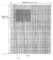
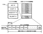
図18は、バンドメモリ1705の内部構成を示す詳細図である。図18において、バンドメモリ1705は、ブラック(Bk)のデータ領域、シアン(CYAN)のデータ領域、マゼンタ(MAGENTA)のデータ領域、イエロー(YELLOW)のデータ領域により構成されている。各色のデータ領域は複数のデータ領域であるバンド1〜Nによって構成されている。各バンド1〜Nは、主走査方向(キャリッジ走査方向)が、印刷シート幅に対応したドット数を保持できる長さに形成されている。また、各バンド1〜Nは、複数のブロックによって構成されている。図18の例では、各ブロックは、主走査方向に16バイト、主走査方向に垂直な紙送り方向に32ライン/バンドの構成となっている。
【0009】
図19は、バンドメモリ1705のアドレス構成を示す図で、バンドメモリ1705中の1ブロックのアドレス構成を示している。尚、図19では、物理アドレスと論理アドレスは一致している。
【0010】
各ブロックは、主走査方向が16バイト/ブロックで紙送り方向が32ライン/ブロックに構成されている。即ち、1ブロックは、主走査方向が16個の升目領域、紙送り方向が32個の升目領域によって構成されている。各升目領域が主走査方向に8ドットの場合、ブロックサイズは128ドット×32ドットのサイズとなる。
【0011】
また、図19は、印刷ドット間隔と印刷ヘッドのノズル間隔は1:1で、印刷ヘッドの複数のノズルが紙送り方向に対して平行に配置されている場合の例であり、縦長の長方形枠で囲んだ8個の升目領域1901は、印刷ヘッドが吐出時に一度に必要とするデータを示している(ノズルが紙送り方向に8個並んだ印刷ヘッドの例)。
【0012】
図17〜図19において、ホストI/F制御ブロックを介して転送される画像データをバンドメモリ1705に記憶する場合、メモリクロックに応答して、図19の左上の升目領域0から右下の升目領域1FFまで、アドレス順に記憶する。これにより、バンドメモリ1705には斜線で示すように、画像データが矩形1902状に配置された状態で記憶される。
【0013】
また、画像データをバンドメモリ1705から読み出す場合には、印刷ヘッドが一度の吐出で必要とする画像データのアドレスは不連続ではあるが、8ビットずつメモリクロックに応答して読み出す。これにより、画像データに応じた印刷が行われる。
【0014】
このように、バンドメモリ1705への画像データの書き込みは、バンドメモリ1705のアドレス順に行われるので、バンドメモリ1705のアドレスは単純にインクリメントすればよく、転送されてきた画像データをスムーズにバンドメモリ1705へ記憶することが可能である。また、バンドメモリ1705へのデータバスを太くした場合、転送されてくるデータを書き込むアドレスが連続しているため、書き込み時に複数バイト同時書き込みが可能になる。
【0015】
【発明が解決しようとする課題】
しかしながら、前述したバンドメモリ1705のアドレス構造では、図20(a)に示すように、データパスを高速化するためにバンドメモリ1705へのデータバスを太く(例えば64ビット)した場合、書込速度(64ビット/クロック)に比べて、読み出し速度(8ビット/クロック)は低くなる。
【0016】
印刷動作を高速化した場合、印刷データのアンダーランを発生させないためにはバンドメモリ1705の読み出し速度を高速化する必要があるが、前記従来のアドレス構造はバンドメモリ読み出し側データパスの高速化を図ることが困難であった。
【0017】
本発明は、印刷速度の高速化を可能にすることを課題としている。
【0018】
【課題を解決するための手段】
本発明によれば、複数のノズルが形成された印刷ヘッドと、印刷する画像データを記憶するバンドメモリと、前記バンドメモリの書込アドレスを生成する書込アドレス生成手段と、前記バンドメモリに記憶した画像データの読出アドレスを生成する読出アドレス生成手段と、前記書込アドレス生成手段で生成した前記バンドメモリのアドレスに前記画像データを記憶するように制御すると共に、前記読出アドレス生成手段で生成した前記バンドメモリのアドレスに記憶した画像データを読み出すように制御するバンドメモリ制御手段とを備え、前記印刷ヘッドを主走査方向に走査すると共に前記主走査方向と直交する紙送り方向に印刷シートを送りつつ、前記バンドメモリから読出した画像データに応じて前記各ノズルからインク滴を吐出することにより、前記印刷シートに印刷を行うインクジェットプリンタにおいて、前記バンドメモリにおける画像データの論理アドレスは、アドレスの下位側から主走査方向アドレスビット、紙送り方向アドレスビットの順に整列した複数のビットによって構成され、前記バンドメモリは前記主走査方向アドレスビットで示される最大のアドレス幅を前記主走査方向に持ち、前記紙送り方向アドレスビットで示される最大のアドレス幅を前記紙送り方向に持ち、紙送り方向の印刷ドット間隔と前記印刷ヘッドのノズル間隔との比が1:2 n を表す紙送り方向解像度データを出力する解像度データ出力手段を備えると共に、前記書込アドレス生成手段は、前記紙送り方向解像度データに基づいて、前記論理アドレスの前記紙送り方向アドレスビットの下位nビットを紙送り方向飛びライン数指定ビットとし、前記論理アドレスビットをアドレス下位側より、前記紙送り方向飛びライン数指定ビットを除く前記紙送り方向アドレスビット、前記主走査方向アドレスビット、前記紙送り方向飛びライン数指定ビットの順に並べ換えて書込アドレスとして出力するアドレス変換手段を備えて成り、前記バンドメモリは前記アドレス変換手段から出力された前記書込アドレスに前記画像データを記憶し、前記バンドメモリ制御手段は前記バンドメモリに記憶された連続する複数の前記書込アドレスで示される前記画像データであって前記バンドメモリ制御手段の読出しに使用するデータバス幅分の前記画像データをメモリクロックに応答して読出すことを特徴とするインクジェットプリンタが提供される。アドレス変換手段は、紙送り方向解像度データを参照して、論理アドレスビットを、紙送り方向アドレスビット、主走査方向アドレスビット、紙送り方向飛びライン数指定ビットの順に並べ換えて書込アドレスとして出力する。バンドメモリは前記アドレス変換手段から出力された前記書込アドレスに画像データを記憶する。
【0020】
ここで、前記書込アドレスに含まれる紙送り方向飛びライン数指定ビットは、印刷ドット間隔と前記複数のノズル間隔が1:2 n のとき、前記紙送り方向で(2 n −1)個おきの画像データに連続したアドレスを付与する値とすることができる。
【0021】
また、前記複数のノズルは前記主走査方向に対して所定角度傾斜した方向に並設され、前記バンドメモリ制御手段は、前記傾斜角度に応じて、入力された画像データをライン毎に主走査方向に所定量シフトして前記バンドメモリに出力する画像データシフト手段を有し、前記バンドメモリは、前記画像データシフト手段からの画像データを前記物理アドレスに記憶するように構成してもよい。
【0022】
【発明の実施の形態】
図1は、本発明の実施の形態に係るインクジェットプリンタのブロック図で、以下説明する各実施の形態に共通するブロック図である。
【0023】
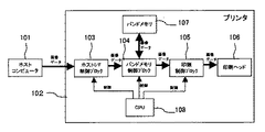
図1において、ホストコンピュータ101からインクジェットプリンタ102に送信された画像データは、ホストコンピュータ101とプリンタ102間のインタフェースであるホストI/F制御ブロック103で受信される。ホストI/F制御ブロック103で受信した前記画像データはバンドメモリ制御ブロック104によって、順次、バンドメモリ107に記憶される。バンドメモリ107に記憶した画像データはバンドメモリ制御ブロック104によって読み出される。印刷制御ブロック105は、バンドメモリ制御ブロック104によって読み出された画像データに応じて、印刷ヘッド106を制御して印刷を行う。尚、ホストI/F制御ブロック103、バンドメモリ制御ブロック104及び印刷制御ブロック105は中央処理装置(CPU)108によって制御される。
【0024】
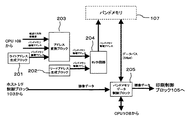
図2は、バンドメモリ制御ブロック104の詳細ブロック図で、以下説明する各実施の形態に共通するブロック図である。尚、図2では、図1と同一部分には同一符号を付している。
【0025】
図2において、ホストI/F制御ブロック103からの画像データは、バンドメモリデータ制御ブロック205を介してバンドメモリ107に入力される。
【0026】
CPU108からの紙送り方向解像度データが、画像データをバンドメモリ107に書き込む際に論理アドレスを物理アドレスに変換するアドレス変換ブロック203に入力される。尚、紙送り方向解像度データとは、印刷ドット間隔とノズル間隔の比を表すデータである。
【0027】
ライトアドレス生成ブロック201は、画像データをバンドメモリ107に書き込む際のバンドメモリ107の論理アドレスを順次生成し、アドレス変換ブロック203に出力する。
【0028】
アドレス変換ブロック203は、前記紙送り方向解像度データを参照して、ライトアドレス生成ブロック201で生成した論理アドレスを、後述するようなアドレス変換処理を行うことにより、画像データを書き込むバンドメモリ107の物理アドレスである書込アドレスをセレクト回路204に順次出力する。
【0029】
リードアドレス生成ブロック202は、画像データをバンドメモリ107から読み出す際に、バンドメモリ107の物理アドレスをアドレス順に出力する。
【0030】
セレクト回路204は、バンドメモリ107へ画像データを書き込むときはアドレス変換ブロック203が発生する物理アドレスをバンドメモリ107に順次出力する。これにより、バンドメモリ107は、アドレス変換ブロック203で発生した物理アドレスに、順次、画像データを記憶する。
【0031】
一方、セレクト回路204は、バンドメモリ107に記憶した画像データを読み出す際に、リードアドレス生成ブロック202が発生する物理アドレスをバンドメモリ107に順次出力する。これにより、バンドメモリ107に記憶した画像データのうち、リードアドレス生成ブロック202で生成した物理アドレスに記憶した画像データが順次読み出されて、バンドメモリデータ制御ブロック205に出力される。バンドメモリデータ制御ブロック205は、入力された画像データを印刷ブロック105へ出力し、印刷ヘッド106が前記画像データに応じた印刷を行う。
【0032】
尚、インクジェットプリンタ102のCPU108からバンドメモリデータ制御ブロック205に入力されるデータは例えばテストパターンのデータであり、又、CPU108からは、前記データを記憶するバンドメモリ107のアドレスを指定するためにアドレス変換ブロック203に論理アドレスが入力される。
【0033】
ライトアドレス生成ブロック201及びアドレス変換手段としてのアドレス変換ブロック203は書込アドレス生成手段を構成し、リードアドレス生成ブロック202は読出アドレス生成手段は構成し又、CPU108は解像度データ出力手段を構成している。また、CPU108、セレクト回路204及びバンドメモリデータ制御ブロック205はバンドメモリ制御手段を構成している。
【0034】
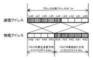
図3は、本発明の第1の実施の形態において、アドレス変換ブロック203のアドレス変換処理を説明するための図で、主走査方向16バイト、紙送り方向32ラインのブロックの例で、且つ、印刷ドット間隔と印刷ヘッド106のノズル間隔との比が1:1の例を示している。CPU108からアドレス変換ブロック203に入力される紙送り方向解像度データは、印刷ドット間隔とノズル間隔の比が1:1であることを表すデータとなる。詳細は後述するが、アドレス変換ブロック203が図3のアドレス変換処理を行うことにより、図19に示したブロックのアドレスを図7に示すブロックのアドレスに変換することができる。
【0035】
図6は、印刷ヘッド106の構成を示す図で、第1乃至第3の実施の形態に共通する構成図である。印刷ヘッド106は、ノズルプレート601に複数(本実施の形態では、主走査方向に対して直角に8個)のノズル602が設けられている。
【0036】
以下、本発明の第1の実施の形態に係るインクジェットプリンタ102の動作を説明する。
【0037】
図3に示すように、画像データの各升目領域の論理アドレスは、9ビット構成のブロック内部アドレスLA0〜LA8によって構成されている。前記論理アドレスは、ブロック内部の主走査方向のアドレスを表す下位4ビットLA0〜LA3、及び、ブロック内部の紙送り方向のアドレスを表す上位5ビットLA4〜LA8によって構成されている。前記論理アドレスは、CPU108やライトアドレス生成ブロック201からアドレス変換ブロック203に入力されるアドレスである。
【0038】
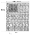
アドレス変換ブロック203は、CPU108からの紙送り方向解像度データを参照して、印刷ドット間隔とノズル間隔の比が1:1であることを判別し、前記論理アドレスの下位4ビットLA0〜LA3を上位ビットPA5〜PA8とし、上位5ビットLA4〜LA8を下位ビットPA0〜PA4とすることによって、論理アドレスの下位ビットLA0〜LA3と上位ビットLA4〜LA8を入れ換えて物理アドレスを生成し、これにより、論理アドレスから物理アドレスへのアドレス変換が行われる。
【0039】
図7は、このようにしてアドレス変換したバンドメモリ107のブロックの物理アドレス構造を示す図である。図7において、バンドメモリ107を構成する各ブロックは、主走査方向が16バイト/ブロックで紙送り方向が32ライン/ブロックに構成されている。即ち、1ブロックは、主走査方向が16個の升目領域、紙送り方向が32個の升目領域によって構成されている。各升目領域が主走査方向に8ドットの場合、ブロックサイズは128ドット×32ドットのサイズとなる。また、図7の例は、印刷ヘッドのノズル配置が主走査方向に対して垂直な場合の例であり、縦長の長方形枠で囲んだ領域701は、印刷ヘッドが吐出時に一度に必要とするデータを示している(ノズルが紙送り方向に8個並んだ印刷ヘッドの例)。
【0040】
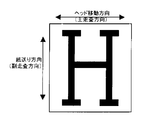
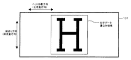
これにより、バンドメモリ107には、図20(b)に示すタイミングで、印刷ヘッドが吐出時に一度に必要とするデータが8ビットずつ連続するアドレスに記憶されると共に、図7の斜線で示すように、矩形の画像データは矩形702の形に配置された状態で記憶される。例えば、印刷データが図8に示すような文字「H」の場合、図9に示すように、バンドメモリ107には、文字「H」がそのままの形で記憶されることになる。
【0041】
画像データをバンドメモリ107から読み出す場合には、セレクト回路204は、リードアドレス生成ブロック202からの物理アドレスをバンドメモリ107に出力する。このとき、リードアドレス生成ブロック202は図20(b)に示すタイミングで、印刷ヘッド106が一度の吐出で必要とする画像データをまとめて、64ビットずつ読み出すようにアドレスを出力する。
【0042】
これにより、バンドメモリ107からは、64ビットずつメモリクロックに応答して読み出される。バンドメモリ107から読み出した画像データは、バンドメモリデータ制御ブロック205を介して印刷制御ブロック105に供給され、印刷ヘッド106によって画像データに応じた印刷が行われる。
【0043】
このように、画像データをバンドメモリ107に書き込む際に、アドレス変換ブロック203によってアドレス変換を行っているため、バンドメモリ107に記憶された画像データをまとめて読み出すことが可能になり、高速読み出しが可能になる。したがって、高速印刷が可能になる。
【0044】
次に、本発明の第2の実施の形態について説明する。図4は、本発明の第2の実施の形態におけるアドレス変換ブロック203の動作を説明する図である。前記第1の実施の形態では、紙送り方向解像度である印刷ドット間隔とノズル間隔の比を1:1としたが、本第2の実施の形態では紙送り方向解像度が1:2(印刷ドット間隔と各ノズル間隔との比が1:2)の例である。
【0045】
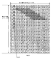
図4に示すように、画像データの各升目領域の論理アドレスは、9ビット構成のブロック内部アドレスLA0〜LA8によって構成されている。前記論理アドレスは、ブロック内部の主走査方向のアドレスを表す下位4ビットLA0〜LA3、紙送り方向解像度に対応するデータを表す中央1ビット(1ライン飛びを指定するためのビット)LA4、及び、ブロック内部の紙送り方向のアドレスを表す上位4ビットLA5〜LA8によって構成されている。
【0046】
アドレス変換部203は、CPU108からの紙送り方向解像度データを参照して、印刷ドット間隔とノズル間隔との比が1:2であることを判別し、紙送り方向解像度に対応する中央ビットLA4を上位ビットPA8に配置し、その下位ビット側に主走査方向のアドレスを表すビットLA0〜LA3を中央ビットPA4からPA7として配置し、その下位ビット側に紙送り方向アドレスLA5〜LA8を下位ビットPA0からPA3として配置する。これにより、論理アドレスから物理アドレスへのアドレス変換が行われ、変換後の物理アドレスに画像データが8ビットずつバンドメモリ107に記憶される。
【0047】
図10は、このようにしてアドレス変換したバンドメモリ107のブロックの物理アドレス構造を示す図である。図10において、各ブロックは、主走査方向が16バイト/ブロックで紙送り方向が32ライン/ブロックに構成されている。即ち、1ブロックは、主走査方向が16個の升目領域、紙送り方向が32個の升目領域によって構成されている。各升目領域が主走査方向に8ドットの場合、ブロックサイズは128ドット×32ドットのサイズとなる。
【0048】
1ラインおきに○印で囲んだ8個の升目領域1001は、印刷ヘッドが吐出時に一度に必要とするデータであり(ノズルが紙送り方向に8個並んだ印刷ヘッドの例)、印刷ヘッド106が一度に必要とする画像データに連続した物理アドレスが付与されている。したがって、リードアドレス生成ブロック202で順次読出アドレスをバンドメモリ107に供給することにより、バンドメモリ107からは、印刷ヘッドが吐出時に一度に必要とする画像データをまとめて一度に読出すことが可能になり、高速読み出しが可能になる。よって、高速印刷が可能になる。尚、バンドメモリ107には、矩形の画像データは斜線で示すような矩形1002の形に記憶されることになる。
【0049】
次に、本発明の第3の実施の形態について説明する。図5は、本第3の実施の形態におけるアドレス変換ブロック203の動作を説明するための図である。前記第2の実施の形態では、紙送り方向解像度は1:2(印刷ドット間隔とノズル間隔の比が1:2)としたが、本第3の実施の形態では紙送り解像度が1:4の例である。
【0050】
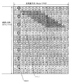
図5に示すように、画像データの各升目領域の論理アドレスは、9ビット構成のブロック内部アドレスLA0〜LA8によって構成されている。前記論理アドレスは、ブロック内部の主走査方向のアドレスを表す下位4ビットLA0〜LA3、紙送り方向解像度に対応するデータを表す中央2ビット(3ライン飛びを指定するためのビット)LA4、LA5、及び、ブロック内部の紙送り方向のアドレスを表す上位3ビットLA6〜LA8によって構成されている。
【0051】
アドレス変換ブロック203は、CPU108からの紙送り方向解像度データが1:4(印刷ドット間隔とノズル間隔の比が1:4)であることを判別し、紙送り方向解像度に対応する中央ビットLA4、LA5を上位ビットPA7、PA8に配置し、その下位ビット側に主走査方向のアドレスを表すビットLA0〜LA3を中央ビットPA3〜PA6として配置し、その下位ビット側に紙送り方向アドレスLA6〜LA8を下位ビットPA0〜PA2として配置する。これにより、論理アドレスから物理アドレスへのアドレス変換が行われ、変換後の物理アドレスに画像データが8ビットずつ順次、バンドメモリ107に記憶される。
【0052】
図11は、このようにしてアドレス変換したバンドメモリ107のブロックの物理アドレス構造を示す図である。図11において、各ブロックは、主走査方向が16バイト/ブロックで紙送り方向が32ライン/ブロックに構成されている。即ち、1ブロックは、主走査方向が16個の升目領域、紙送り方向が32個の升目領域によって構成されている。各升目領域が主走査方向に8ドットの場合、ブロックサイズは128ドット×32ドットのサイズとなる。
【0053】
3ラインおきに○印で囲んだ8個の升目領域1101は、印刷ヘッドが吐出時に一度に必要とするデータであり(ノズルが紙送り方向に8個並んだ印刷ヘッドの例)、印刷ヘッド106が一度に必要とする画像データに連続した物理アドレスが付与されている。したがって、リードアドレス生成ブロック202で順次読出アドレスをバンドメモリ107に供給することにより、バンドメモリ107からは、印刷ヘッドが吐出時に一度に必要とする画像データをまとめて一度に読出すことが可能になり、高速読み出しが可能になる。よって、高速印刷が可能になる。尚、バンドメモリ107には、矩形の画像データは斜線で示すような矩形1102の形に記憶されることになる。
【0054】
次に、本発明の第4の実施の形態に係るインクジェットプリンタについて説明する。
【0055】
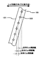
図12は、第4〜第6の実施の形態に共通する印刷ヘッド106の構成を示す図である。印刷ヘッド106は、ノズルプレート1201に複数(本実施の形態では、主走査方向に対して所定角度傾斜して8個)のノズル1202が形成されている。
【0056】
ライトアドレス生成ブロック201は、CPU205から主走査方向に対する複数ノズル1202の配列方向の傾斜角の情報を受信して、印刷ヘッド106が一度に必要とする画像データが紙送り方向に整列するように主走査方向に対する複数のノズル1202の傾斜角に合わせて、各ライン毎の書込開始位置を所定量(本実施の形態ではブロック内升目領域1個分)シフトさせた論理アドレスを生成する。ここで、ライトアドレス生成ブロック201は論理アドレスシフト手段を構成している。
【0057】
一方、図3に示すように、画像データの各升目領域の論理アドレスは、9ビット構成のブロック内部アドレスLA0〜LA8によって構成されている。前記論理アドレスは、ブロック内部の主走査方向のアドレスを表す下位4ビットLA0〜LA3、及び、ブロック内部の紙送り方向のアドレスを表す上位5ビットLA4〜LA8によって構成されている。
【0058】
アドレス変換ブロック203は、CPU108からの紙送り方向解像度データが1:1(印刷ドット間隔とノズル間隔との比が1:1)であることを判別し、前記論理アドレスの下位4ビットLA0〜LA3を上位ビットPA5〜PA8とし、上位5ビットLA4〜LA8を下位ビットPA0〜PA4とすることによって、論理アドレスの下位ビットLA0〜LA3と上位ビットLA4〜LA8を入れ換えた書込アドレスを生成する。これにより、論理アドレスから物理アドレスへのアドレス変換が行われる。
【0059】
画像データ書込み時には、アドレス変換ブロック203で生成した物理アドレスがセレクト回路204を介してバンドメモリ107に出力される。バンドメモリデータ制御ブロック205から出力された画像データは、バンドメモリ107の前記物理アドレスに記憶される。
【0060】
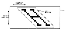
図13は、前記の如くしてアドレス変換したバンドメモリ107内ブロックの物理アドレス構造を示す図である。図13において、各ブロックは、主走査方向が16バイト/ブロックで紙送り方向が32ライン/ブロックに構成されている。即ち、1ブロックは、主走査方向が16個の升目領域、紙送り方向が32個の升目領域によって構成されている。各升目領域が主走査方向に8ドットの場合、ブロックサイズは128ドット×32ドットのサイズとなる。
【0061】
8個の升目を縦長の長方形枠で囲んだ領域1301は、印刷ヘッドが吐出時に一度に必要とするデータであり(ノズルが紙送り方向に8個並んだ印刷ヘッドの例)、印刷ヘッド106が一度に必要とする画像データに連続した物理アドレスが付与されている。したがって、リードアドレス生成ブロック202で順次読出アドレスをバンドメモリ107に供給することにより、バンドメモリ107からは、印刷ヘッドが吐出時に一度に必要とするデータをまとめて一度に読み出すことが可能になり、高速読み出しが可能になる。
【0062】
尚、バンドメモリ107には、矩形の画像データは斜線で示すような平行四辺形1302の形に記憶されることになる。図14は、これを説明するための図で、画像データが「H」の場合、図8に示すような矩形配置の画像データ「H」が、バンドメモリ107には、平行四辺形配置の画像データに変換されて記憶されることになる。
【0063】
画像データをバンドメモリ107から読み出す場合には、セレクト回路204は、リードアドレス生成ブロック202からの物理アドレスをバンドメモリ107に出力する。このとき、図20(b)に示すように、リードアドレス生成ブロック202は、印刷ヘッドが一度の吐出で必要とする画像データをまとめて、64ビットずつ読み出すようにアドレスを出力する。これにより、バンドメモリ107からは、64ビットずつメモリクロックに応答して読出される。バンドメモリ107から読出した画像データは、バンドメモリデータ制御ブロック205を介して印刷制御ブロック105に供給され、印刷ヘッド106によって画像データに応じた印刷が行われる。
【0064】
このように、画像データをバンドメモリ107に書き込む際に、アドレス変換ブロック203によってアドレス変換を行っているため、バンドメモリ107に記憶された画像データをまとめて読み出すことが可能になり、高速読み出しが可能になる。したがって、高速印刷が可能になる。また、印刷ヘッド106は、主走査方向に対して所定角度傾斜して配設された複数のノズル1202を有する構成であるため、高解像度の印刷を行うことが可能になる。
【0065】
次に、本発明の第5の実施の形態について説明する。前記第4の実施の形態では、紙送り方向解像度は1:1(印刷ドット間隔とノズル間隔との比が1:1)としたが、本第5の実施の形態では紙送り方向解像度が1:2の例である。
【0066】
ライトアドレス生成ブロック201は、CPU205から主走査方向に対する複数ノズル1202の配列方向の傾斜角の情報を受信して、印刷ヘッド106が一度に必要とする画像データが紙送り方向に整列するように主走査方向に対する複数のノズル1202の傾斜角に合わせて、各ライン毎の書込開始位置を所定量(本実施の形態ではブロック内升目領域1個分)シフトさせた論理アドレスを生成する。ここで、ライトアドレス生成ブロック201は論理アドレスシフト手段を構成している。
【0067】
一方、図4に示すように、画像データの各升目領域の論理アドレスは、9ビット構成のブロック内部アドレスLA0〜LA8によって構成されている。前記論理アドレスは、ブロック内部の主走査方向のアドレスを表す下位4ビットLA0〜LA3、紙送り方向解像度に対応するデータを表す中央1ビット(1ライン飛びを指定するためのビット)LA4、及び、ブロック内部の紙送り方向のアドレスを表す上位4ビットLA5〜LA8によって構成されている。
【0068】
アドレス変換部203は、CPU103からの紙送り方向解像度が1:2であると判別し、紙送り方向解像度に対応する中央ビットLA4を上位ビットPA8に配置し、その下位ビット側に主走査方向のアドレスを表すビットLA0〜LA3を中央ビットPA4からPA7として配置し、その下位ビット側に紙送り方向アドレスLA5〜LA8を下位ビットPA0からPA3として配置することによって、物理アドレスを生成する。これにより、論理アドレスから物理アドレスへのアドレス変換が行われる。
【0069】
画像データ書込み時には、アドレス変換ブロック203で生成した物理アドレスがセレクト回路204を介してバンドメモリ107に出力される。バンドメモリデータ制御ブロック205から出力された画像データは、バンドメモリ107の前記物理アドレスに記憶される。
【0070】
図15は、このようにしてアドレス変換したバンドメモリ107内ブロックの物理アドレス構造を示す図である。図15において、各ブロックは、主走査方向が16バイト/ブロックで紙送り方向が32ライン/ブロックに構成されている。即ち、1ブロックは、主走査方向が16個の升目領域、紙送り方向が32個の升目領域によって構成されている。各升目領域が主走査方向に8ドットの場合、ブロックサイズは128ドット×32ドットのサイズとなる。
【0071】
1ラインおきに○印で囲んだ8個の升目領域1501は、印刷ヘッドが吐出時に一度に必要とするデータであり(ノズルが紙送り方向に8個並んだ印刷ヘッドの例)、印刷ヘッド106が一度に必要とする画像データに連続した物理アドレスが付与されている。したがって、リードアドレス生成ブロック202で順次読出アドレスをバンドメモリ107に供給することにより、バンドメモリ107からは、印刷ヘッドが吐出時に一度に必要とするデータをまとめて一度に読出すことが可能になり、高速読み出しが可能になる。尚、バンドメモリ107には、矩形の画像データは斜線で示すような平行四辺形1502の画像データとして記憶されることになる。
【0072】
画像データをバンドメモリ107から読み出す場合には、前記第4の実施の形態と同様にして、リードアドレス生成ブロック202からの物理アドレスに記憶されたバンドメモリ107内画像データが64ビット毎にまとめて読出されて印刷される。
【0073】
このように、画像データをバンドメモリ107に書き込む際に、アドレス変換ブロック203によってアドレス変換を行っているため、バンドメモリ107に記憶された画像データをまとめて読み出すことが可能になり、高速読み出しが可能になる。したがって、高速印刷が可能になる。また、印刷ヘッド106は、主走査方向に対して所定角度傾斜して配設された複数のノズル1202を有する構成であるため、高解像度の印刷を行うことが可能になる。
【0074】
次に、本発明の第6の実施の形態について説明する。前記第5の実施の形態では、紙送り方向解像度は1:2としたが、本第6の実施の形態では紙送り解像度が1:4の例である。
【0075】
ライトアドレス生成ブロック201は、CPU205から主走査方向に対する複数ノズル1202の配列方向の傾斜角の情報を受信して、印刷ヘッド106が一度に必要とする画像データが紙送り方向に整列するように主走査方向に対する複数のノズル1202の傾斜角に合わせて、各ライン毎の書込開始位置を所定量(本実施の形態ではブロック内升目領域1個分)シフトさせた論理アドレスを生成する。ここで、ライトアドレス生成ブロック201は論理アドレスシフト手段を構成している。
【0076】
一方、図5に示すように、画像データの各升目領域の論理アドレスは、9ビット構成のブロック内部アドレスLA0〜LA8によって構成されている。前記論理アドレスは、ブロック内部の主走査方向のアドレスを表す下位4ビットLA0〜LA3、紙送り方向解像度に対応するデータを表す中央2ビット(3ライン飛びを指定するためのビット)LA4、LA5、及び、ブロック内部の紙送り方向のアドレスを表す上位3ビットLA6〜LA8によって構成されている。
【0077】
アドレス変換部203は、CPU103からの紙送り方向解像度が1:4であると判別し、紙送り方向解像度に対応する中央ビットLA4、LA5を上位ビットPA7、PA8に配置し、その下位ビット側に主走査方向のアドレスを表すビットLA0〜LA3を中央ビットPA3からPA6として配置し、その下位ビット側に紙送り方向アドレスLA6〜LA8を下位ビットPA0からPA2として配置することによって、物理アドレスを生成する。これにより、論理アドレスから物理アドレスへのアドレス変換が行われる。
【0078】
画像データ書込み時には、アドレス変換ブロック203で生成した物理アドレスがセレクト回路204を介してバンドメモリ107に出力される。バンドメモリデータ制御ブロック205から出力された画像データは、バンドメモリ107の前記物理アドレスに記憶される。
【0079】
図16は、このようにしてアドレス変換したバンドメモリ107内ブロックの物理アドレス構造を示す図である。図16において、各ブロックは、主走査方向が16バイト/ブロックで紙送り方向が32ライン/ブロックに構成されている。即ち、1ブロックは、主走査方向が16個の升目領域、紙送り方向が32個の升目領域によって構成されている。各升目領域が主走査方向に8ドットの場合、ブロックサイズは128ドット×32ドットのサイズとなる。
【0080】
3ラインおきに○印で囲んだ8個の升目領域1601は、印刷ヘッドが吐出時に一度に必要とするデータであり(ノズルが紙送り方向に8個並んだ印刷ヘッドの例)、印刷ヘッド106が一度に必要とする画像データに連続した物理アドレスが付与されている。したがって、リードアドレス生成ブロック202で順次読出アドレスをバンドメモリ107に供給することにより、バンドメモリ107からは、印刷ヘッドが吐出時に一度に必要とするデータをまとめて一度に読み出すことが可能になり、高速読み出しが可能になる。尚、バンドメモリ107には、矩形の画像データは斜線で示すような平行四辺形1602の画像データとして記憶されることになる。
【0081】
画像データをバンドメモリ107から読み出す場合には、前記第5の実施の形態と同様にして、リードアドレス生成ブロック202からの物理アドレスに記憶されたバンドメモリ107内画像データが64ビット毎にまとめて読出されて印刷される。
【0082】
このように、画像データをバンドメモリ107に書き込む際に、アドレス変換ブロック203によってアドレス変換を行っているため、バンドメモリ107に記憶された画像データをまとめて読み出すことが可能になり、高速読み出しが可能になる。したがって、高速印刷が可能になる。また、印刷ヘッド106は、主走査方向に対して所定角度傾斜して配設された複数のノズル1202を有する構成であるため、高解像度の印刷を行うことが可能になる。
【0083】
以上述べたように、本発明の実施の形態に係るインクジェットプリンタは、特に、複数のブロックに区切られたバンドメモリにおける画像データの論理アドレスは各部ロック毎に主走査方向アドレスビットと紙送り方向アドレスビットとによって構成されると共に、書込アドレス生成手段は前記主走査方向アドレスビットと紙送り方向アドレスビットとを入れ換えて得られるアドレスを各ブロックにおける書込アドレスとして前記バンドメモリに出力するアドレス変換手段を備えて成り、前記バンドメモリは前記アドレス変換手段から出力された前記書込アドレスに前記画像データを記憶することを特徴としている。したがって、バンドメモリ107からの画像データ読出速度が高速になるため、高速印刷が可能になる。
【0084】
また、バンドメモリの各ブロックにおける画像データの論理アドレスは、主走査方向アドレスビット、紙送り方向の飛びライン数を表す紙送り方向飛びライン数指定ビット、紙送り方向アドレスビットの順に整列した複数のビットによって構成され、紙送り方向の印刷ドット間隔と前記印刷ヘッドのノズル間隔との比を表す紙送り方向解像度データを出力する解像度データ出力手段を備えると共に、前記書込アドレス生成手段は、前記紙送り方向解像度データを参照して、前記論理アドレスビットを、アドレス下位側より前記紙送り方向アドレスビット、主走査方向アドレスビット、紙送り方向飛びライン数指定ビットの順に並べ換えて各ブロックの書込アドレスとして出力するアドレス変換手段を備えて成り、前記バンドメモリは前記アドレス変換手段から出力された前記書込アドレスに前記画像データを記憶することを特徴としている。また、各ブロックにおいて前記書込アドレスに含まれる紙送り方向飛びライン数指定ビットは、印刷ドット間隔と複数のノズル間隔が1:nのとき、各ブロックにおいて紙送り方向で(n−1)個おきの画像データに連続したアドレスを付与する値としている。したがって、印刷ヘッドに応じた高解像度の印刷が可能になる。
【0085】
また、複数のノズルは主走査方向に対して所定角度傾斜した方向に並設され、ライトアドレス生成手段は、前記傾斜角度に応じて、入力された画像データを各ブロックのライン毎に主走査方向に所定量シフトして前記バンドメモリに書き込むための、アドレスシフト手段を有し、前記バンドメモリは、前記画像データシフト手段からの画像データを前記物理アドレスに記憶するように構成している。したがって、主走査方向に対して所定角度傾斜した印刷ヘッドを使用して、高解像度の印刷が可能になる。
【0086】
【発明の効果】
本発明によれば、高速な印刷を行うことが可能になる。また、主走査方向に対して所定角度傾斜した印刷ヘッドを使用することにより、高解像度の印刷が可能になる。
【図面の簡単な説明】
【図1】 本発明の実施の形態に係るインクジェットプリンタのブロック図である。
【図2】 本発明の実施の形態に係るインクジェットプリンタの要部ブロック図である。
【図3】 本発明の第1、第4の実施の形態に係るインクジェットプリンタの説明図である。
【図4】 本発明の第2、第5の実施の形態に係るインクジェットプリンタの説明図である。
【図5】 本発明の第3、第6の実施の形態に係るインクジェットプリンタの説明図である。
【図6】 本発明の第1〜第3の実施の形態に係るインクジェットプリンタのノズル配置を示す図である。
【図7】 本発明の第1の実施の形態に係るインクジェットプリンタのバンドメモリのアドレス構成を示す図である。
【図8】 本発明の実施の形態に係るインクジェットプリンタの説明図である。
【図9】 本発明の第1〜第3の実施の形態に係るインクジェットプリンタの説明図である。
【図10】 本発明の第2の実施の形態に係るインクジェットプリンタのバンドメモリのアドレス構成を示す図である。
【図11】 本発明の第3の実施の形態に係るインクジェットプリンタのバンドメモリのアドレス構成を示す図である。
【図12】 本発明の第4〜第6の実施の形態に係るインクジェットプリンタのノズル配置を示す図である。
【図13】 本発明の第4の実施の形態に係るインクジェットプリンタのバンドメモリのアドレス構成を示す図である。
【図14】 本発明の第4〜第6の実施の形態に係るインクジェットプリンタの説明図である。
【図15】 本発明の第5の実施の形態に係るインクジェットプリンタのバンドメモリのアドレス構成を示す図である。
【図16】 本発明の第6の実施の形態に係るインクジェットプリンタのバンドメモリのアドレス構成を示す図である。
【図17】 従来のインクジェットプリンタの要部ブロック図である。
【図18】 一般的なバンドメモリの構成を示す図である。
【図19】 従来のインクジェットプリンタのバンドメモリのアドレス構成を示す図である。
【図20】 インクジェットプリンタのタイミング図である。
【符号の説明】
101・・・ホストコンピュータ
102・・・インクジェットプリンタ
103・・・ホストI/F制御ブロック
104・・・バンドメモリ制御ブロック
105・・・印刷制御ブロック
106・・・印刷ヘッド
107、1705・・・バンドメモリ
108・・・バンドメモリ制御手段を構成するCPU
201・・・書込アドレス生成手段を構成するライトアドレス生成ブロック
202・・・読出アドレス生成手段を構成するリードアドレス生成ブロック
203・・・アドレス変換手段を構成するアドレス変換ブロック
204・・・バンドメモリ制御手段を構成するセレクト回路
205、1704・・・バンドメモリ制御手段を構成するバンドメモリデータ制御ブロック
601、1201・・・ノズルプレート
602、1202・・・ノズル[0001]
BACKGROUND OF THE INVENTION
The present invention relates to an ink jet printer that prints images such as characters and graphics on a print sheet by ejecting ink droplets from nozzles in accordance with image data read from a band memory.
[0002]
[Prior art]
Conventionally, a print head having a plurality of nozzles formed thereon, a band memory for storing image data to be printed, a write address generating means for generating a write address for the band memory, and image data stored in the band memory Read address generating means for generating a read address of the band memory, and controlling the image data to be stored in the address of the band memory generated by the write address generating means, and the band memory generated by the read address generating means Band memory control means for controlling to read out image data stored at the address, and scanning the print head in the main scanning direction and feeding the print sheet in the paper feeding direction orthogonal to the main scanning direction, Ink droplets are ejected from each nozzle according to the image data read from the band memory. More, the ink jet printer for printing an image such as characters and graphics corresponding to the image data to the printing sheet is used.
[0003]
The inkjet printer includes a memory (band memory) that temporarily stores image data to be printed partially (in a band), and supplies the print head with a drive signal corresponding to the data stored in the band memory at a predetermined timing. Printing corresponding to the image data is performed. The address for storing the image data in the band memory is configured to simply increment in the main scanning direction of the carriage on which the print head is mounted.
[0004]
FIG. 17 is a block diagram of the main part of a conventional inkjet printer. In FIG. 17, image data from a host I / F control block that is an interface with a host computer is input to a
[0005]
When the
[0006]
When reading the image data stored in the
[0007]
The CPU data input from the internal CPU of the inkjet printer to the band memory
[0008]
FIG. 18 is a detailed diagram showing the internal configuration of the
[0009]
FIG. 19 is a diagram showing the address configuration of the
[0010]
Each block has a main scanning direction of 16 bytes / block and a paper feed direction of 32 lines / block. That is, one block is composed of 16 square areas in the main scanning direction and 32 square areas in the paper feed direction. When each square area is 8 dots in the main scanning direction, the block size is 128 dots × 32 dots.
[0011]
FIG. 19 shows an example in which the print dot interval and the nozzle interval of the print head are 1: 1, and a plurality of nozzles of the print head are arranged in parallel to the paper feed direction. Eight
[0012]
17 to 19, when image data transferred via the host I / F control block is stored in the
[0013]
Further, when reading image data from the
[0014]
As described above, the writing of the image data to the
[0015]
[Problems to be solved by the invention]
However, in the address structure of the
[0016]
When the printing operation is accelerated, it is necessary to increase the reading speed of the
[0017]
An object of the present invention is to make it possible to increase the printing speed.
[0018]
[Means for Solving the Problems]
According to the present invention, a print head in which a plurality of nozzles are formed, a band memory that stores image data to be printed, a write address generation unit that generates a write address of the band memory, and a memory stored in the band memory A read address generating means for generating a read address of the image data, and a control for storing the image data at the address of the band memory generated by the write address generating means, and the read address generating means Band memory control means for controlling the image data stored at the address of the band memory to be read out, and scans the print head in the main scanning direction and feeds the print sheet in the paper feeding direction orthogonal to the main scanning direction. While ejecting ink droplets from each nozzle according to the image data read from the band memory It allows in an inkjet printer for printing on the printing sheet, the logical address of the image data in the band memory in the main scanning direction address bits from low-order address,paperThe band memory has a maximum address width indicated by the main scanning direction address bits in the main scanning direction, and includes the paper feeding direction address bits.InThe maximum address width shown is in the paper feed direction, and the ratio between the print dot interval in the paper feed direction and the nozzle interval of the print head1: 2 n Resolution data output means for outputting paper feed direction resolution data representing the write address generation means,,in frontBased on the paper feed direction resolution data,The lower n bits of the paper feed direction address bits of the logical addressPaper feed direction jump line number specification bitAndAnd the logical address bits from the lower address side,Excluding the paper feed direction jump line number specification bitThe band memory comprises address conversion means for rearranging the paper feed direction address bits, the main scanning direction address bits, and the paper feed direction jump line number designation bits in order, and outputting them as write addresses. The image data is stored at the output write address, and the band memory control means is the band memory control means that is the image data indicated by the plurality of continuous write addresses stored in the band memory. There is provided an ink jet printer characterized in that the image data corresponding to a data bus width used for reading is read in response to a memory clock. The address conversion means refers to the paper feed direction resolution data and rearranges the logical address bits in the order of the paper feed direction address bit, the main scanning direction address bit, and the paper feed direction jump line number designation bit, and outputs it as a write address. . The band memory stores the image data at the write address output from the address converting means.
[0020]
Here, in the paper feed direction jump line number designation bit included in the write address, the print dot interval and the plurality of nozzle intervals are 1:2 n In the paper feed direction (2 n -1) It can be a value that gives consecutive addresses to every other image data.
[0021]
The plurality of nozzles are juxtaposed in a direction inclined by a predetermined angle with respect to the main scanning direction, and the band memory control means converts the input image data into the main scanning direction for each line according to the inclination angle. The image data from the image data shift means may be stored in the physical address.
[0022]
DETAILED DESCRIPTION OF THE INVENTION
FIG. 1 is a block diagram of an ink jet printer according to an embodiment of the present invention, and is a block diagram common to each embodiment described below.
[0023]
In FIG. 1, image data transmitted from the
[0024]
FIG. 2 is a detailed block diagram of the band
[0025]
In FIG. 2, the image data from the host I / F control block 103 is input to the
[0026]
Paper feed direction resolution data from the
[0027]
The write address generation block 201 sequentially generates a logical address of the
[0028]
The
[0029]
When reading image data from the
[0030]
The
[0031]
On the other hand, the
[0032]
The data input from the
[0033]
The write
[0034]
FIG. 3 is a diagram for explaining the address conversion process of the
[0035]
FIG. 6 is a diagram illustrating the configuration of the
[0036]
Hereinafter, the operation of the
[0037]
As shown in FIG. 3, the logical address of each square area of the image data is configured by 9-bit block internal addresses LA0 to LA8. The logical address is composed of lower 4 bits LA0 to LA3 representing addresses in the main scanning direction inside the block and upper 5 bits LA4 to LA8 representing addresses in the paper feed direction inside the block. The logical address is an address input from the
[0038]
The
[0039]
FIG. 7 is a diagram showing the physical address structure of the block of the
[0040]
As a result, the
[0041]
When reading image data from the
[0042]
Thus, 64 bits are read from the
[0043]
As described above, when the image data is written in the
[0044]
Next, a second embodiment of the present invention will be described. FIG. 4 is a diagram for explaining the operation of the
[0045]
As shown in FIG. 4, the logical address of each cell area of the image data is configured by 9-bit block internal addresses LA0 to LA8. The logical address includes the lower 4 bits LA0 to LA3 representing the address in the main scanning direction inside the block, the central 1 bit (bit for designating one line skip) LA4 representing the data corresponding to the paper feed direction resolution, and It is composed of upper 4 bits LA5 to LA8 representing addresses in the paper feed direction inside the block.
[0046]
The
[0047]
FIG. 10 is a diagram showing a physical address structure of a block of the
[0048]
Eight square areas 1001 surrounded by circles every other line are data that the print head needs at the time of ejection (an example of a print head in which eight nozzles are arranged in the paper feed direction). Are assigned consecutive physical addresses to image data required at one time. Therefore, the read address generation block 202 sequentially supplies the read address to the
[0049]
Next, a third embodiment of the present invention will be described. FIG. 5 is a diagram for explaining the operation of the
[0050]
As shown in FIG. 5, the logical address of each square area of the image data is configured by 9-bit block internal addresses LA0 to LA8. The logical address is composed of lower 4 bits LA0 to LA3 representing addresses in the main scanning direction inside the block, central 2 bits (bits for designating 3 line jumps) LA4, LA5 representing data corresponding to the paper feed direction resolution, The upper three bits LA6 to LA8 that represent addresses in the paper feed direction inside the block are also configured.
[0051]
The
[0052]
FIG. 11 is a diagram showing a physical address structure of a block of the
[0053]
Eight
[0054]
Next, an ink jet printer according to a fourth embodiment of the present invention will be described.
[0055]
FIG. 12 is a diagram showing the configuration of the
[0056]
The write
[0057]
On the other hand, as shown in FIG. 3, the logical address of each cell area of the image data is configured by 9-bit block internal addresses LA0 to LA8. The logical address is composed of lower 4 bits LA0 to LA3 representing addresses in the main scanning direction inside the block and upper 5 bits LA4 to LA8 representing addresses in the paper feed direction inside the block.
[0058]
The
[0059]
When writing image data, the physical address generated by the
[0060]
FIG. 13 is a diagram showing the physical address structure of the block in the
[0061]
A
[0062]
In the
[0063]
When reading image data from the
[0064]
As described above, when the image data is written in the
[0065]
Next, a fifth embodiment of the present invention will be described. In the fourth embodiment, the paper feed direction resolution is 1: 1 (ratio of print dot interval to nozzle interval is 1: 1). However, in the fifth embodiment, the paper feed direction resolution is 1 : 2 example.
[0066]
The write
[0067]
On the other hand, as shown in FIG. 4, the logical address of each square area of the image data is configured by 9-bit block internal addresses LA0 to LA8. The logical address includes the lower 4 bits LA0 to LA3 representing the address in the main scanning direction inside the block, the central 1 bit (bit for designating one line skip) LA4 representing the data corresponding to the paper feed direction resolution, and It is composed of upper 4 bits LA5 to LA8 representing addresses in the paper feed direction inside the block.
[0068]
The
[0069]
When writing image data, the physical address generated by the
[0070]
FIG. 15 is a diagram showing the physical address structure of the block in the
[0071]
Eight
[0072]
When the image data is read from the
[0073]
As described above, when the image data is written in the
[0074]
Next, a sixth embodiment of the present invention will be described. In the fifth embodiment, the paper feed direction resolution is 1: 2, but in the sixth embodiment, the paper feed resolution is 1: 4.
[0075]
The write
[0076]
On the other hand, as shown in FIG. 5, the logical address of each cell area of the image data is configured by 9-bit block internal addresses LA0 to LA8. The logical address is composed of lower 4 bits LA0 to LA3 representing addresses in the main scanning direction inside the block, central 2 bits (bits for designating 3 line jumps) LA4, LA5 representing data corresponding to the paper feed direction resolution, The upper three bits LA6 to LA8 that represent addresses in the paper feed direction inside the block are also configured.
[0077]
The
[0078]
When writing image data, the physical address generated by the
[0079]
FIG. 16 is a diagram showing the physical address structure of the block in the
[0080]
Eight
[0081]
When the image data is read from the
[0082]
As described above, when the image data is written in the
[0083]
As described above, in the inkjet printer according to the embodiment of the present invention, in particular, the logical address of the image data in the band memory divided into a plurality of blocks is the main scanning direction address bit and the paper feed direction address for each lock. The address conversion means for outputting to the band memory an address obtained by replacing the main scanning direction address bit and the paper feed direction address bit as a writing address in each block. The band memory stores the image data at the write address output from the address conversion means. Therefore, the image data reading speed from the
[0084]
Further, the logical address of the image data in each block of the band memory has a plurality of lines arranged in the order of the main scanning direction address bit, the paper feed direction jump line number designation bit indicating the number of jump lines in the paper feed direction, and the paper feed direction address bit. A resolution data output unit configured to output a paper feed direction resolution data that is configured by a bit and represents a ratio between a print dot interval in the paper feed direction and a nozzle interval of the print head; and the write address generation unit includes the paper Referring to the feed direction resolution data, the logical address bits are rearranged in the order of the paper feed direction address bit, the main scanning direction address bit, and the paper feed direction jump line number designation bit from the lower address side, and the write address of each block Address conversion means for outputting as Is characterized by storing the image data to output said write address from the scan converter. Further, the paper feed direction jump line number designation bit included in the write address in each block is (n−1) pieces in the paper feed direction in each block when the print dot interval and the plurality of nozzle intervals are 1: n. It is a value that gives consecutive addresses to every other image data. Therefore, high-resolution printing according to the print head is possible.
[0085]
The plurality of nozzles are juxtaposed in a direction inclined at a predetermined angle with respect to the main scanning direction, and the write address generating means converts the input image data for each line of each block according to the inclination angle in the main scanning direction. Address shift means for shifting to a predetermined amount and writing to the band memory, and the band memory is configured to store the image data from the image data shift means at the physical address. Therefore, high-resolution printing is possible using a print head inclined at a predetermined angle with respect to the main scanning direction.
[0086]
【The invention's effect】
According to the present invention, high-speed printing can be performed. Further, by using a print head inclined at a predetermined angle with respect to the main scanning direction, high-resolution printing can be performed.
[Brief description of the drawings]
FIG. 1 is a block diagram of an ink jet printer according to an embodiment of the present invention.
FIG. 2 is a principal block diagram of the ink jet printer according to the embodiment of the present invention.
FIG. 3 is an explanatory diagram of an ink jet printer according to first and fourth embodiments of the present invention.
FIG. 4 is an explanatory diagram of an ink jet printer according to second and fifth embodiments of the present invention.
FIG. 5 is an explanatory diagram of an ink jet printer according to third and sixth embodiments of the present invention.
FIG. 6 is a diagram showing the nozzle arrangement of the ink jet printer according to the first to third embodiments of the present invention.
FIG. 7 is a diagram showing an address configuration of a band memory of the ink jet printer according to the first embodiment of the present invention.
FIG. 8 is an explanatory diagram of an ink jet printer according to an embodiment of the present invention.
FIG. 9 is an explanatory diagram of an ink jet printer according to first to third embodiments of the present invention.
FIG. 10 is a diagram showing an address configuration of a band memory of an ink jet printer according to a second embodiment of the present invention.
FIG. 11 is a diagram showing an address configuration of a band memory of an ink jet printer according to a third embodiment of the present invention.
FIG. 12 is a diagram showing the nozzle arrangement of the ink jet printer according to the fourth to sixth embodiments of the present invention.
FIG. 13 is a diagram showing an address configuration of a band memory of an ink jet printer according to a fourth embodiment of the present invention.
FIG. 14 is an explanatory diagram of ink jet printers according to fourth to sixth embodiments of the present invention.
FIG. 15 is a diagram showing an address configuration of a band memory of an ink jet printer according to a fifth embodiment of the present invention.
FIG. 16 is a diagram showing an address configuration of a band memory of an ink jet printer according to a sixth embodiment of the present invention.
FIG. 17 is a principal block diagram of a conventional inkjet printer.
FIG. 18 is a diagram showing a configuration of a general band memory.
FIG. 19 is a diagram illustrating an address configuration of a band memory of a conventional inkjet printer.
FIG. 20 is a timing chart of the ink jet printer.
[Explanation of symbols]
101... Host computer
102: Inkjet printer
103 ... Host I / F control block
104: Band memory control block
105: Print control block
106... Print head
107, 1705 ... Band memory
108... CPU constituting band memory control means
201... Write address generation block constituting write address generation means
202... Read address generation block constituting read address generation means
203 ... Address translation block constituting address translation means
204... Select circuit constituting band memory control means
205, 1704... Band memory data control block constituting band memory control means
601, 1201 ... nozzle plate
602, 1202 ... Nozzle
Claims (3)
前記バンドメモリにおける画像データの論理アドレスは、アドレスの下位側から主走査方向アドレスビット、紙送り方向アドレスビットの順に整列した複数のビットによって構成され、前記バンドメモリは前記主走査方向アドレスビットで示される最大のアドレス幅を前記主走査方向に持ち、前記紙送り方向アドレスビットで示される最大のアドレス幅を前記紙送り方向に持ち、
紙送り方向の印刷ドット間隔と前記印刷ヘッドのノズル間隔との比が1:2 n を表す紙送り方向解像度データを出力する解像度データ出力手段を備えると共に、前記書込アドレス生成手段は、前記紙送り方向解像度データに基づいて、前記論理アドレスの前記紙送り方向アドレスビットの下位nビットを紙送り方向飛びライン数指定ビットとし、前記論理アドレスビットをアドレス下位側より、前記紙送り方向飛びライン数指定ビットを除く前記紙送り方向アドレスビット、前記主走査方向アドレスビット、前記紙送り方向飛びライン数指定ビットの順に並べ換えて書込アドレスとして出力するアドレス変換手段を備えて成り、前記バンドメモリは前記アドレス変換手段から出力された前記書込アドレスに前記画像データを記憶し、前記バンドメモリ制御手段は前記バンドメモリに記憶された連続する複数の前記書込アドレスで示される前記画像データであって前記バンドメモリ制御手段の読出しに使用するデータバス幅分の前記画像データをメモリクロックに応答して読出すことを特徴とするインクジェットプリンタ。A print head in which a plurality of nozzles are formed; a band memory for storing image data to be printed; a write address generating means for generating a write address for the band memory; and a read address for the image data stored in the band memory A read address generating means for generating the image data, and controlling the image data to be stored at the address of the band memory generated by the write address generating means, and at the address of the band memory generated by the read address generating means Band memory control means for controlling to read out the stored image data, scanning the print head in the main scanning direction and feeding the print sheet in the paper feeding direction orthogonal to the main scanning direction, from the band memory By ejecting ink droplets from each nozzle according to the read image data, In the ink-jet printer for printing on the printing sheet,
The logical address of the image data in the band memory is composed of a plurality of bits arranged in the order of main scanning direction address bits and paper feed direction address bits from the lower side of the address, and the band memory is indicated by the main scanning direction address bits. has a maximum address width in the main scanning direction, it has a maximum address range indicated by the paper feed direction address bit to the paper feeding direction,
The ratio of the print dot spacing in the paper feeding direction and the nozzle spacing of the print head 1: provided with a resolution data output means for outputting the paper feed direction resolution data representing the 2 n, said write address generating means, before Symbol based on the paper feed direction resolution data, wherein the lower n bits of said paper feeding direction address bits of the logical address to the paper feeding direction skipping line number specified bits, from said logical address bits address lower, the paper feeding direction The band includes address conversion means for rearranging the paper feed direction address bits excluding the jump line number designation bits , the main scanning direction address bits, and the paper feed direction jump line number designation bits and outputting them as write addresses. The memory stores the image data at the write address output from the address conversion means, and Memory control means uses the image data corresponding to the data bus width used for reading of the band memory control means, which is the image data indicated by a plurality of consecutive write addresses stored in the band memory, as a memory clock. An ink jet printer characterized by reading in response.
Priority Applications (1)
| Application Number | Priority Date | Filing Date | Title |
|---|---|---|---|
| JP2001302530A JP4704635B2 (en) | 2001-09-28 | 2001-09-28 | Inkjet printer |
Applications Claiming Priority (1)
| Application Number | Priority Date | Filing Date | Title |
|---|---|---|---|
| JP2001302530A JP4704635B2 (en) | 2001-09-28 | 2001-09-28 | Inkjet printer |
Publications (2)
| Publication Number | Publication Date |
|---|---|
| JP2003103846A JP2003103846A (en) | 2003-04-09 |
| JP4704635B2 true JP4704635B2 (en) | 2011-06-15 |
Family
ID=19122760
Family Applications (1)
| Application Number | Title | Priority Date | Filing Date |
|---|---|---|---|
| JP2001302530A Expired - Fee Related JP4704635B2 (en) | 2001-09-28 | 2001-09-28 | Inkjet printer |
Country Status (1)
| Country | Link |
|---|---|
| JP (1) | JP4704635B2 (en) |
Families Citing this family (4)
| Publication number | Priority date | Publication date | Assignee | Title |
|---|---|---|---|---|
| JP2006192607A (en) * | 2005-01-11 | 2006-07-27 | Fuji Photo Film Co Ltd | Method and device for preparing frame data, frame data-preparation program, and method and device for drawing |
| JP5074733B2 (en) * | 2005-09-30 | 2012-11-14 | キヤノン株式会社 | Recording device |
| DE102006029088A1 (en) * | 2006-06-24 | 2007-12-27 | Man Roland Druckmaschinen Ag | Method for printing a substrate |
| JP7357240B2 (en) * | 2020-02-25 | 2023-10-06 | パナソニックIpマネジメント株式会社 | Control method for inkjet printing device and inkjet printing device |
Family Cites Families (4)
| Publication number | Priority date | Publication date | Assignee | Title |
|---|---|---|---|---|
| JPS6225568A (en) * | 1985-07-25 | 1987-02-03 | Matsushita Electric Ind Co Ltd | How to write image data |
| JP2849260B2 (en) * | 1992-01-21 | 1999-01-20 | キヤノン株式会社 | Image processing device |
| JP3703273B2 (en) * | 1997-11-14 | 2005-10-05 | キヤノン株式会社 | Image data conversion apparatus, printing apparatus including image data conversion apparatus, and image data conversion method |
| JP2001191587A (en) * | 2000-01-14 | 2001-07-17 | Copyer Co Ltd | Printing device and print data processing method |
-
2001
- 2001-09-28 JP JP2001302530A patent/JP4704635B2/en not_active Expired - Fee Related
Also Published As
| Publication number | Publication date |
|---|---|
| JP2003103846A (en) | 2003-04-09 |
Similar Documents
| Publication | Publication Date | Title |
|---|---|---|
| EP1658988B1 (en) | Combination of bidirectional- and undirectional-printing using plural ink types | |
| JP2731908B2 (en) | Printer driving method | |
| TWI283639B (en) | Improvements relating to print engines | |
| JP4205849B2 (en) | Color inkjet head | |
| KR100612022B1 (en) | Method and apparatus for printing inkjet printer with wide print head | |
| US8419152B2 (en) | Recording apparatus | |
| JPH07276794A (en) | Method and device for printing graphic image | |
| JPS61104856A (en) | Ink jet color print head | |
| JP4704635B2 (en) | Inkjet printer | |
| JP4691880B2 (en) | An image output device that outputs an image while converting resolution of data of a plurality of pixel columns in which dots are formed simultaneously | |
| US20030137556A1 (en) | Draft printing with multiple same-hue ink nozzles | |
| JP2011076156A (en) | Apparatus and method for processing image | |
| JP3829587B2 (en) | Draft printing using nozzles that eject ink of the same hue as nozzles that eject the same type of ink | |
| JP2963032B2 (en) | Printing apparatus and printing method | |
| JP2004255700A (en) | Dot data creation processing considering saving of memory capacity | |
| JPH0958019A (en) | Image forming device | |
| JP3088863B2 (en) | Recording device | |
| JPS592855A (en) | Inkjet printer | |
| JP2000238249A (en) | Ink jet recording device | |
| JP3167433B2 (en) | Inkjet printer | |
| JP2007301742A (en) | Inkjet recording apparatus, data processing method, program, and storage medium | |
| JP2008000920A (en) | Inkjet recording apparatus and image processing method | |
| JP2006007583A (en) | Printing method | |
| JP2001138513A (en) | Position shift adjustment in printing using multiple types of drive signals | |
| JPH11115165A (en) | Ink-jet printer |
Legal Events
| Date | Code | Title | Description |
|---|---|---|---|
| RD01 | Notification of change of attorney |
Free format text: JAPANESE INTERMEDIATE CODE: A7421 Effective date: 20040303 |
|
| A711 | Notification of change in applicant |
Free format text: JAPANESE INTERMEDIATE CODE: A711 Effective date: 20070601 |
|
| A621 | Written request for application examination |
Free format text: JAPANESE INTERMEDIATE CODE: A621 Effective date: 20080805 |
|
| RD01 | Notification of change of attorney |
Free format text: JAPANESE INTERMEDIATE CODE: A7421 Effective date: 20091105 |
|
| RD01 | Notification of change of attorney |
Free format text: JAPANESE INTERMEDIATE CODE: A7421 Effective date: 20091112 |
|
| RD01 | Notification of change of attorney |
Free format text: JAPANESE INTERMEDIATE CODE: A7421 Effective date: 20091118 |
|
| A131 | Notification of reasons for refusal |
Free format text: JAPANESE INTERMEDIATE CODE: A131 Effective date: 20100810 |
|
| A521 | Request for written amendment filed |
Free format text: JAPANESE INTERMEDIATE CODE: A523 Effective date: 20101007 |
|
| A131 | Notification of reasons for refusal |
Free format text: JAPANESE INTERMEDIATE CODE: A131 Effective date: 20101124 |
|
| A521 | Request for written amendment filed |
Free format text: JAPANESE INTERMEDIATE CODE: A523 Effective date: 20110118 |
|
| A131 | Notification of reasons for refusal |
Free format text: JAPANESE INTERMEDIATE CODE: A131 Effective date: 20110208 |
|
| A521 | Request for written amendment filed |
Free format text: JAPANESE INTERMEDIATE CODE: A523 Effective date: 20110217 |
|
| TRDD | Decision of grant or rejection written | ||
| A01 | Written decision to grant a patent or to grant a registration (utility model) |
Free format text: JAPANESE INTERMEDIATE CODE: A01 Effective date: 20110308 |
|
| A61 | First payment of annual fees (during grant procedure) |
Free format text: JAPANESE INTERMEDIATE CODE: A61 Effective date: 20110310 |
|
| R150 | Certificate of patent or registration of utility model |
Ref document number: 4704635 Country of ref document: JP Free format text: JAPANESE INTERMEDIATE CODE: R150 |
|
| RD04 | Notification of resignation of power of attorney |
Free format text: JAPANESE INTERMEDIATE CODE: R3D04 |
|
| R250 | Receipt of annual fees |
Free format text: JAPANESE INTERMEDIATE CODE: R250 |
|
| R250 | Receipt of annual fees |
Free format text: JAPANESE INTERMEDIATE CODE: R250 |
|
| R250 | Receipt of annual fees |
Free format text: JAPANESE INTERMEDIATE CODE: R250 |
|
| S111 | Request for change of ownership or part of ownership |
Free format text: JAPANESE INTERMEDIATE CODE: R313111 |
|
| R350 | Written notification of registration of transfer |
Free format text: JAPANESE INTERMEDIATE CODE: R350 |
|
| LAPS | Cancellation because of no payment of annual fees |