JP4703089B2 - Mounting board production equipment - Google Patents
Mounting board production equipment Download PDFInfo
- Publication number
- JP4703089B2 JP4703089B2 JP2002218706A JP2002218706A JP4703089B2 JP 4703089 B2 JP4703089 B2 JP 4703089B2 JP 2002218706 A JP2002218706 A JP 2002218706A JP 2002218706 A JP2002218706 A JP 2002218706A JP 4703089 B2 JP4703089 B2 JP 4703089B2
- Authority
- JP
- Japan
- Prior art keywords
- mounting
- unit
- electronic component
- substrate
- width
- Prior art date
- Legal status (The legal status is an assumption and is not a legal conclusion. Google has not performed a legal analysis and makes no representation as to the accuracy of the status listed.)
- Expired - Fee Related
Links
Images


Description
【0001】
【発明の属する技術分野】
本発明は、電子部品を基板に装着する電子部品装着装置および実装基板生産装置に関する。
【0002】
【従来の技術】
従来より、プリント基板等の基板に電子部品を実装する際には、基板にクリーム状のはんだペーストを印刷する工程、印刷されたはんだペーストに電子部品を装着する工程、および、電子部品が装着された基板を加熱および冷却してはんだを固化させ、電子部品を基板に固着させる工程とが行われる。
【0003】
図12は基板に電子部品を実装する従来の実装システムのうち、電子部品を基板に装着させる電子部品装着システム9の構成を示す斜視図である。電子部品装着システム9では、印刷装置より矢印901にて示す方向からはんだペーストが印刷された基板が搬入され、搬送路902に沿って電子部品装着システム9内を基板が搬送される。基板には搬送される間に各種電子部品が装着され、矢印903にて示す方向へと基板が搬出される。その後、基板はリフロー装置へと搬入され、電子部品が基板に固着される。
【0004】
図12に示す電子部品装着システム9では、3つの高速装着装置91および2つの多機能装着装置92が順に配置され、高速装着装置91と多機能装着装置92との間には電子部品の装着状態を検査する検査装置93が配置される。なお、高速装着装置91は微小な電子部品を高速にて多数基板に装着する装置であり、多機能装着装置92は多種類の電子部品を基板に装着する装置である。
【0005】
【発明が解決しようとする課題】
ところで、図12に示す電子部品装着システム9は大型の基板に対しても電子部品の装着が可能となるように設計されたものである。一方で、携帯電話を含む携帯端末の普及に伴い、携帯端末に組み込まれる基板の小型化も推し進められている。
【0006】
したがって、電子部品装着システム9を用いて携帯端末用の基板に効率よく電子部品を装着するためには、搬送される1枚の基板に多数台分の携帯端末の回路を形成する必要がある。
【0007】
しかしながら、携帯端末の多様化に伴って基板の多品種少量生産(実装)の要望が強くなりつつあり、図12に示す電子部品装着システム9は、携帯端末用基板への電子部品の装着には必ずしも適した構成ではなくなりつつある。
【0008】
従って、本発明の目的は、上記課題に鑑みなされたものであり、小型基板の製造に適した電子部品装着装置および実装基板生産装置を提供することにある。
【0009】
【課題を解決するための手段】
上記目的を達成するために、本発明は以下のように構成する。
【0022】
本発明の第1態様によれば、基板上に半田を介在させて電子部品を装着させる装着作業部と、上記半田をリフローさせて上記電子部品を上記基板上に固定させて実装基板を生産するリフロー作業部とを備えて、上記装着作業部及び上記リフロー作業部に上記基板を搬送させながら、上記基板より上記実装基板を生産する実装基板生産装置において、
上記実装基板生産装置は、
上記装着作業部を有し、かつ上記基板の搬送方向沿いの実質的装置幅が270mm以上330mm以下の範囲から選択される1つの基準寸法の整数倍の寸法であるとともに450mm以上1000mm以下の寸法とされている複数の第1ユニット装置と、
上記リフロー作業部を有し、かつ上記基板の上記搬送方向沿いの実質的装置幅が上記基準寸法の2以上の整数倍の寸法とされている第2ユニット装置と、
を備え、
上記それぞれの第1ユニット装置及び上記第2ユニット装置は、上記搬送方向に沿って連設されて、移動可能に固定され、
上記第1ユニット装置は、上記基板に上記電子部品を装着する電子部品装着装置であり、
上記電子部品装着装置は、
上記電子部品を供給する電子部品供給部と、
上記搬送方向に上記基板を、基板待機位置から部品装着位置に、さらに、上記部品装着位置から部品装着位置外にそれぞれ搬送可能な搬送部と、
上記電子部品供給部の上記電子部品を基板に装着するヘッド部と、
上記電子部品供給部と上記基板との間で上記ヘッド部を移動させる駆動部と、
上記電子部品装着装置の正面に、第1ヒンジにて回動可能に設けられた保護カバーと、
上記保護カバーと上記ヘッド部との間に設けられ、第2ヒンジにて回動可能に設けられた操作盤と、
を備える、実装基板生産装置を提供する。
本発明の第2態様によれば、上記第1ヒンジは、上記電子部品装着装置の上端に設けられ、
上記第2ヒンジは、上記操作盤の上端に設けられた、第1態様に記載の実装基板生産装置を提供する。
【0023】
本発明の第3態様によれば、上記操作盤は、デイスプレイと、操作ボタンとを含む、第1又は2の態様に記載の実装基板生産装置を提供する。
【0024】
本発明の第4態様によれば、上記操作盤は、上記電子部品装着装置の内部に設けられた、第1から3の態様いずれか1つに記載の実装基板生産装置を提供する。
【0025】
本発明の第5態様によれば、上記電子部品装着装置の実質的装置幅は、上記電子部品装着装置のフレームの幅、または、上記保護カバーの幅である、第1から4の態様いずれか1つに記載の実装基板生産装置を提供する。
【0026】
本発明の第6態様によれば、上記支柱は、ねじ軸部であり、上記支柱昇降機構は、上記ねじ軸部に螺合したナット部であり、上記ねじ軸部を上記ナット部に対して相対的に正逆回転させることにより、上記支柱昇降機構に取り付けられた上記支柱を昇降させる第4の態様に記載の実装基板生産装置を提供する。
【0027】
本発明の第7態様によれば、上記固定機構は、さらに、上記支柱昇降機構により下降された上記支柱の先端部と係合可能な凹部を有しかつ上記設置面上に設置される支柱受部とを備える第4の態様に記載の実装基板生産装置を提供する。
【0033】
【発明の実施の形態】
本発明の記述を続ける前に、添付図面において同じ部品については同じ参照符号を付している。
【0034】
以下に、本発明にかかる実施の形態を図面に基づいて詳細に説明する。
【0035】
(第1実施形態)
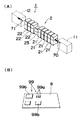
図1(A)は本発明の第1実施形態に係る実装基板生産装置1内の複数の電子部品装着装置より構成される電子部品装着システム2の外観を示す斜視図である。図1(B)は上記電子部品装着システム2の複数の電子部品装着装置で電子部品99が実装された基板8の斜視図である。電子部品装着システム2は、基板8に電子部品99を実装する実装基板生産装置1において、はんだペーストの印刷装置11とリフロー装置12との間に配置される。
【0036】
電子部品装着システム2は、5台の(電子部品装着装置の一例としての)高速装着装置21と3台の(電子部品装着装置の別の例としての)多機能装着装置22とを有し、高速装着装置21と多機能装着装置22との間には電子部品の装着状態を検査する検査装置23が配置される。そして、高速装着装置21、検査装置23および多機能装着装置22とが一列に配置されることにより、これら装置内部に基板8の搬送路が形成される。
【0037】
印刷装置11からは矢印70にて示す方向へとはんだペーストが印刷された基板8が高速装着装置21に搬入され、基板8のはんだペースト上には5台の高速装着装置21により多数の微小な電子部品99aが順次装着される。その後、検査装置23にて電子部品の装着が適切に行われたか否かが検査され、検査に合格した基板8には多機能装着装置22により比較的大きな様々な電子部品99bが装着される。
【0038】
各種電子部品99の装着が完了した基板8は、電子部品装着システム2から矢印71にて示す方向に搬出され、リフロー装置12へと搬入される。これにより、はんだペーストの溶融および固化が行われ、基板に対する電子部品99の実装が完了する。
【0039】
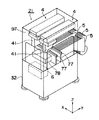
図2は高速にて電子部品を基板に装着する高速装着装置21の正面、右側面および平面を示す外観斜視図である。なお、多品種の電子部品を基板に装着する多機能装着装置22は、部品の供給形態や保持形態が異なる点を除いて高速装着装置21と同じ構造となっている。また、図2中に示すXYZ方向は、それぞれ、正面に向かって右側から左側に向かう方向、正面から背後に向かう方向、および、下方から上方へ向かう方向を示している。
【0040】
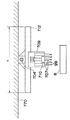
高速装着装置21は、上部カバー31と下部カバー32とに覆われた略直方体の形状をしており、上部カバー31の前面は開閉自在な保護カバー75となっている。保護カバー75には2つの開口75a,75bが上下に形成されており、保護カバー75の内側には上側の開口75aに対向して操作盤33が配置される。下側の開口75bには透明のアクリル板が取り付けられ、装置内部を確認するための窓81となっている。
【0041】
上部カバー31と下部カバー32との間には、高速装着装置21内部を左右に貫通する平行な一対の搬送レール部材77が敷設されており、一対の搬送レール部材77が僅かに突出する高速装着装置21の左右の開口は基板搬出入口98とされる。そして、後述するように、一対の搬送レール部材77の基板搬送用ベルトの駆動により、基板8は一対の搬送レール部材77上を所定の搬送方向((+X)方向)へと搬送される。
【0042】
図3は、上部カバー31や操作盤33等を省略することにより高速装着装置21の内部構造を示す斜視図である。図3に示すように、上部カバー31内には電子部品を装着するための2つの装着機構4がX方向に並んで配置され、高速装着装置21の背後からは多数の部品カセット5が取り付けられる。なお、図3では、装着機構4を支持するフレーム97を透視して描かれている。
【0043】
一対の搬送レール部材77は搬送駆動部78に接続されており、搬送駆動部78は、モータを駆動して、モータの動力伝達機構に連結された幅寄せ機構により1対の搬送レール部材77の間の間隔を調整したり、モータからの動力伝達機構を切り替えて、一対の搬送レール部材77内の基板搬送用ベルトの正逆駆動を行う。なお、一対の搬送レール部材77では、右端から左端に向けて、待機位置位置決め用搬送用ベルト、装着位置位置決め用搬送用ベルト、待機位置位置決め用搬送用ベルト、装着位置位置決め用搬送用ベルト、装着位置外への搬送用搬送用ベルトが一対ずつ配置されて、それぞれの搬送用ベルトが互いに独立して搬送駆動部78により駆動制御されるようにしてもよい。
【0044】
また、装着機構4、部品カセット5、搬送駆動部78等を制御するための制御部6が下部カバー32内に収納される。したがって、高速装着装置21は周囲に他の装置が存在しない単独の状態でも動作可能とされる。
【0045】
高速装着装置21では、装着機構4のヘッド部41が部品カセット5から電子部品99を受け取り、一対の搬送レール部材77上を搬送されてきた基板8に電子部品99を装着するという動作が繰り返し行われるが、各構成の詳細について説明する前に、まず、高速装着装置21の大きさおよび構成の配置に関して説明する。なお、高速装着装置21の大きさおよび構成の配置に関する以下の説明は、多機能装着装置22にも同様に適用される。
【0046】
高速装着装置21は、小型の基板(例えば、一辺が250mm未満の四角形の基板)に電子部品を装着する専用機として設計されている。すなわち、携帯電話を含む携帯端末用の小さな基板を製造するための専用機となっている。これにより、生産能力は従来の1つの大型製造ラインよりも低下するが、歩留まりおよび基板品種の切替の点で有利な製造が実現される。
【0047】
具体的には、小型基板を扱うことにより大型基板(例えば、一辺が250mm以上の四角形の基板)よりも1枚の基板の廃棄により生じる損失が抑えられる。また、小型基板専用の装置として高速装着装置21自体の小型化を図ることにより、基板品種の切替の際の大がかりな作業負担が低減される。なお、高速装着装置21自体の小型化により、同一の敷地において従来よりも多数の製造ラインを設置することが可能となる。したがって、設置面積当りの生産性は必ずしも低下する訳ではなく、向上する場合もある。
【0048】
また、同一面積の敷地に多数のラインを設置することにより、1つのラインが停止してしまったときの生産能力の低下を抑えることも実現される。このように、小型基板専用の小型の高速装着装置21を用いることにより新たな付加価値を得ることができる。なお、図12に示す従来の電子部品装着システム9と比べ、図1(A)に示す電子部品装着システム2の長さは、高速装着装置21および多機能装着装置22の小型化により、1/4〜1/3へと抑えられている。
【0049】
以上の理由により、高速装着装置21は小型基板専用として小型化が図られた装着装置として設計されているが、さらに、高速装着装置21の大きさおよび構造は、人間工学的見地および生産性への配慮に基づいて最適化されている。
【0050】
図4に示すように正面からみて装置の幅(すなわち、搬送方向に対する実質的装置幅)をAWとし、装置の高さをHとした場合、装置の小型化(正確には、占有面積の縮小)を図ると高さHは高くならざるを得ない。しかしながら、図5に示すように人間が装置のメンテナスや初期調整、駆動操作などの作業を行うことができる、すなわち作業性を考慮した高さMHは、通常、2000mm程度であるため、装置の高さHも2000mm程度に制限することが好ましい。また安全性の面からも台座などを使用せずに手を伸ばせる必要性からも装置の高さHも2000mm程度に制限することが好ましい。このような観点から、装置の高さは1300〜2000mm程度が使用される。
【0051】
ところで、高速装着装置21の新規設置あるいはライン構成の組み替えに際しては、高速装着装置21を運搬する必要がある。このとき、装置の幅AWがあまりに小さいと高速装着装置21を安定して支持することが困難となってしまう。ここで、装置の重心が装置の中央に存在し、装置の傾きが20°程度になったとしても装置の姿勢が元の起立姿勢となるように復元力が生じる必要があるものと仮定した場合、高さHと幅AWとは、次の数式の関係を満たす必要がある。
【0052】
【数1】
H・tan20°<AW
【0053】
その結果、高さHが1300mm程度の場合には幅AWは少なくとも450mm必要であり、高さHが2000mm程度の場合には幅AWは少なくとも600mm必要であると結論づけることができる。このために装置の設置時に仮に装置が傾いても倒れることなく姿勢復帰が可能となり、装置自体に生じる損傷、負荷を軽減することが可能となる。
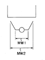
一方で、図6に示すように、人が高速装着装置21に対向して操作や作業を行う場合、装置幅AWがあまりに小さいと操作や作業が困難となる。特に装置内にある部品カセット5の取り付けや、ヘッド部41、搬送レール部材77の給油や初期値調整、ノズルノズル86の交換、認識カメラの調整などの装置内部の作業には労を要する。
【0054】
また、配列配置された複数の高速装着装置21のうちの1台を撤去し、撤去により生じた隙間に人が入って作業する場合、特に装置の下部の作業では腰を曲げる作業を行なう必要性があるので、最低450mmの隙間が存在しないと作業自体が不可能となってしまう。一般に、人の幅MW1は600〜650mm程度であり、人が入り込む隙間としては最低600mm存在することが好ましいことから、より好ましくは装置の幅AWは600mm程度とされる必要がある。
【0055】
以上のことから、人間工学的見地から、あるいは、作業性の見地から高速装着装置21の幅AWは450mm以上であることが必要であり、600mm程度(「程度」として10%の範囲を考えた場合、540〜660mmとなる。)とされることがより好ましいといえる。
【0056】
もちろん、装置の幅AWが大きいほど、装置の姿勢が安定するとともに装置が撤去された際に生じる隙間も大きくなる。しかしながら、装置が大型化すると、既述のように基板品種の切り替え作業や装置の入れ替え作業が大掛かりなものとなってしまい、多品種の小型基板を取り扱うという観点からは好ましいとはいえない。また、装置幅AWが大きくなりすぎた場合、1台の装置に対して操作や確認作業を行う際に人が移動する必要が生じる。したがって、装置の幅AWは人が両腕を広げつつ作業を行うことができる幅MW2である1000mm以下に抑えられることが好ましい。
【0057】
以上のように、小型基板専用の装着装置としては、幅が450mm以上1000mm以下であることが好ましく、600mm程度であることがより好ましいといえる。そこで、高速装着装置21では幅AWが約600mmとされている。
【0058】
なお、装置の幅AWは実質的な幅をいい、装置外周に存在する突起や取り付けられた部材を含まない。具体的には、図3に示すように装置および作業者を保護するためにヘッド部41を含む装着機構4がカバーに覆われている場合は、カバーにより規定される幅が実質的装置の幅ということができ、仮に、装置がカバーに覆われていない場合には装置のフレームにより規定される幅が実質的装置幅であると規定することができる。
【0059】
図7は2つの装着機構4を下方から見た様子を示す図である。装着機構4のヘッド部41は部品カセット5から吸着により電子部品を受け取る10個のノズル86を有し、リニアモータを駆動源とする、駆動部の一例としての駆動機構42によりX方向に移動可能とされる。さらに、駆動機構42もリニアモータを駆動源とする、駆動部の一例としての駆動機構43によりY方向に移動可能とされる。したがって、駆動機構42および駆動機構43により構成される機構が移動の際に必要とする移動領域は図7中に符号83にて示す領域となる。
【0060】
なお、ヘッド部41の各ノズル86は、上下に昇降可能であるとともにZ方向を向く軸を中心に回動可能とされる。これにより、ノズル86が吸着した電子部品を様々な方向に向けて基板に装着することが可能とされる。
【0061】
図7に示すように、2つの装着機構4の移動領域83は互いに重なり合わずに独立とされる。これにより、2つの装着機構4の制御を独立して行うことができ、制御に関するプログラミングが容易とされる。また、ヘッド部41と同数だけ駆動機構42,43が存在するため、ヘッド部41の制御を完全に独立して行うことができ、一層容易に制御を行うことができる。
【0062】
高速装着装置21では、図3に示すように装着機構4が2つ配置される。これは、既述のように装置幅AWを600mm程度とした場合であって小型基板専用の装置として設計する場合、通常の構成ではあるが小型化が図られた装着機構4の大きさに鑑みて装着機構4を2つ配置することが最適な設計となるからである。特に、図7に示すように装着機構4の移動領域83が干渉しない場合には装着機構4の剛性や入手可能なリニアモータの大きさを考慮すると装着機構4を2つとすることが好ましい。
【0063】
さらに、高速装着装置21では、装着機構4や部品カセット5等が左右対称(搬送方向に対して垂直な方向からみて左右対称)となるように配置される。高速装着装置21は占有床面積を小さく抑えるために高さ方向に長い構造となっている。したがって、高速装着装置21は搬送される際に左右に傾いてしまう可能性が高い。そこで、高速装着装置21では、ほぼ左右対称となる構造を採用することにより、高速装着装置21の搬送や据え付けの際に姿勢が安定するようにされている。なお、上述の数1は高速装着装置21の重心がほぼ中央にあることを前提としているが、このような前提は高速装着装置21がほぼ左右対称構造である点を考慮したものである。
【0064】
また、基板8の四角形の1辺の長さは、例えば、1000mmを等分することにより決定される。したがって、基板の四角形(例えば正方形)の1辺の長さとしては、500mm、330mm、250mm、200mm等が採用される。もし、基板の正方形の1辺の長さが100mmならば、縦10個×横10個の合計100個の基板が連結された、正方形の1辺の長さが1000mmの一枚の多数個取り用の基板8となる。ここで、四角形の1辺の長さが250mm未満の小型基板を扱う場合、装置幅AWを約600mmにすると装置内に存在することができる基板8を物理的に2以上とすることができる。その結果、装着機構4を1つ配置するよりも2つ配置する方が適切な設計となる。
【0065】
図8は、ヘッド部41の下方の構成を示す平面図である。以下、図7および図8を参照しながら高速装着装置21の動作について説明する。なお、図8では100mm角の基板8に電子部品99の装着が行われる場合を例示している。
【0066】
1対の搬送レール部材77に挟まれるようにして基板8が、1台目の装着機構4に対して、装置外から基板待機位置P1、そして基板待機位置P1から装着機構4のおよそ下方の部品装着位置P2に位置すると(2台目の装着機構4に対して、1台目の装着機構4の部品装着位置P2から基板待機位置P3、そして基板待機位置P3から2台目の装着機構4の装着機構4のおよそ下方の部品装着位置P2に位置すると)、ヘッド部41が部品カセット5側へと移動する。部品カセット5は図3に示すように電子部品99が載置されたテープが捲回されたリールを有し、テープがリールから部品カセット5の先端(一対の搬送レール部材77側の先端)へと繰り出されることにより、電子部品99が一対の搬送レール部材77側へと供給される。
【0067】
なお、通常、装置の小型化を図る場合、電子部品99の供給を搬送経路の両側から行うことにより多種類の電子部品99の装着が行われる。この場合、予備の電子部品99、すなわち、交換用の部品カセット5を装置の前方にも後方にも配置する必要が生じ、結局、実装システムの実質的な小型化の妨げとなってしまう。しかしながら、高速装着装置21では、図8に示すように一対の搬送レール部材77の一方側のみに部品カセット5を位置させる。これにより、装置の小型化を図りつつも予備の電子部品99を装置の後方のみに準備するだけで済み、実質的な占有面積の削減が確実に図られる。
【0068】
図7および図8において、符号84にて示す領域は、ヘッド部41のノズル86が電子部品99の吸着を行う領域を示している。領域84にて部品カセット5から電子部品99が取り出されると、ヘッド部41は基板8上へと移動する。なお、図7中に符号85にて示す領域は、ヘッド部41が基板8に電子部品99の装着を行う領域を示しており、基板8はこの領域85内に配置される。図8に示す例では、高速装着装置21において100mmの基板8が取り扱われ、一対の搬送レール部材77上の待機位置P1、部品装着位置P2、待機位置P1、部品装着位置P2に配置される4枚の基板8のうち、2つの装着機構4の真下の部品装着位置P2に位置する2枚の基板8に電子部品99の装着が同時に行われる。
【0069】
駆動機構42および駆動機構43によりヘッド部41が基板8の上方に位置すると、各ノズル86の向き(大略水平面内でのノズル中心軸周りの回転方向の向き)が調整された上でノズル86が下降し、電子部品99が基板8上のはんだペーストに装着される。図8では図示を省略しているが、ノズル86に電子部品99が吸着された際にカメラを用いて電子部品99の吸着状態が確認される。
【0070】
以上に説明した動作により、装着機構4による電子部品99の部品カセット5からの吸着、および、基板8への電子部品99の装着が繰り返し行われ、2つの装着機構4の真下のの部品装着位置P2の2枚の基板8に必要なだけの電子部品99が装着される。電子部品99の装着が完了すると、搬送駆動部78による一対の搬送レール部材77の駆動により、基板8は、図8において右から左((+X)方向)へ部品装着位置P2から部品装着位置P2外の位置へと搬送され、新たな基板8が、待機位置P1又はP3から装着機構4の真下の部品装着位置P2に配置される。このとき、1枚の基板8が高速装着装置21の右側面から一対の搬送レール部材77上に搬入され、左端の1枚の基板8が左側面から一対の搬送レール部材77外に搬出される。
【0071】
次に、図8を参照しながら複数の高速装着装置21が配列配置される様子について説明する。
【0072】
図8に示すように、互いに隣接する高速装着装置21の間の隙間(以下、単に「装置の間の距離」という。)は非常に狭く抑えられる。例えば、図8では高速装着装置21の装置幅AWが600mmであり、隣接する2台の高速装着装置21間の間隙Cが55mmとされる。一対の搬送レール部材77が装置側面から突出する長さが25mmであり、隣接する装置における一対の搬送レール部材77間の間隙が5mmとされる。これにより、高速装着装置21の幅AWを抑えるとともに複数の高速装着装置21を配列配置した際の電子部品装着システム2の長さも短く抑えられる。
【0073】
一般に、従来の装着装置の間の距離は、基板を作業者が取り除くことができる長さとされてきている(ただし、特に大きな基板を取り扱う場合を除く)。すなわち、基板の長さのうち搬送方向に平行な長さよりも装置と装置との間の距離が長く設定されてきている。このような設定は、装着不良の基板を装置から搬出された直後に必要に応じて取り除くことを可能とすることを目的としている。
【0074】
これに対して、上記第1実施形態にかかる高速装着装置21では、小型基板、特に、搬送方向の基板幅が250mm未満の基板を扱うにも関わらず、装置と装置との間の距離が、搬送方向の基板幅以下に設定されることができる。これにより、電子部品装着システム2の長さを非常に短くすることが実現され(すなわち、実装基板生産装置1の長さを短くすることが実現される。)、実装基板生産装置1全体を設置する際のレイアウトに自由度を持たせることができる。
【0075】
さらに、実装基板生産装置1の長さが短くなることから、必然的に搬送ライン上に載置される基板8の個数(特に、電子部品装着システム2に存在する基板8の個数)が削減される。その結果、仕掛かり基板8の個数を減少させることができ、基板8の品種切替や装着システムのトラブル時に廃棄される基板8の数を少なくすることも実現される。
【0076】
次に、高速装着装置21における操作盤33について説明する。高速装着装置21では装置幅AWが小さく抑えられるため、操作盤33が従来と異なる手法により取り付けられる。通常、装置と装置との間が十分に広い場合は、操作盤は装置と装置との間に配置される。また、装置の高さが低い場合には、操作盤は装置の上部に配置される。
【0077】
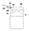
既述のように高速装着装置21では、装置と装置との間の長さが小さく設定され、かつ、装置幅AWを小さく抑えるために装置の高さが高く設定されることができる。したがって、操作盤33は装置内部に配置される。少なくとも、装置間の距離が操作盤33の幅よりも小さい場合には、操作盤33は装置の上方か装置内部に配置する必要があり、装置の高さが1500mmを超える場合には操作性の観点から操作盤33を装置内に配置せざるを得ない。高速装着装置21では、図2に示すように、操作盤33は前面の保護カバー75とヘッド部41との間に配置される。
【0078】
操作盤33は、図2に示すように、操作者に向けて各種情報を表示するディスプレイ74、操作者からの各種操作を受け付ける操作ボタン79、非常停止のための停止ボタン80等が配置される。保護カバー75は、第1待避機構の一例としての上端の1対のヒンジ73により回動可能に支持される。これにより、図9に示す状態から図10に示す状態へとヒンジ73を中心として保護カバー75は開閉自在とされる。
【0079】
ところが、図10に示す状態においては、ヘッド部41の下方に対する作業を行うことができるものの装着機構4の上部やヘッド部41の正面に対する作業は、操作盤33が遮蔽物体となって困難となる。
【0080】
そこで、高速装着装置21では、操作盤33の上端に、第2待避機構の一例としてヒンジ76を設け、図10に示す状態から図11に示す状態へと操作盤33がヒンジ76を中心に回動可能とされる。これにより、ディスプレイ74を含む操作盤33がヘッド部41に対して待避可能となり、ヘッド部41に対する作業や装着機構4の上方への作業も容易に行うことが実現される。
【0081】
以上、本発明に係る第1実施形態について説明してきたが、本発明は上記実施形態に限定されるものではなく様々な変形が可能である。
【0082】
例えば、上記説明では高速装着装置21の小型化について主として説明したが、既述のように、電子部品99の供給形態やヘッド部41のノズル形状を変更することにより、多品種の電子部品99の装着を行う多機能装着装置22についても同様の設計を行うことができる。すなわち、部品99の供給形態はテープ式に限定されるものではなく、トレイ上に電子部品99を配置するトレイ式やその他の方式が採用されてもよい。さらには、電子部品99はノズル86にて吸着されて保持されるものに限定されず、メカニカルチャック等のように他の方式にて電子部品99がヘッド部41に保持されてもよい。このように、上記第1実施形態に係る装着装置は様々な電子部品99を基板8上に装着する装着装置に利用することができる。なお、下記の様々な変形例に関しても多機能装着装置22に適用することができる。
【0083】
上記第1実施形態では、基板8は一対の搬送レール部材77に沿って直線的に搬送されるが、およそ搬送方向が決定されているのであるならば、搬送方向は厳密に直線である必要はない。例えば、基板8に電子部品99が装着される際にノズル86を下降させる代わりに基板8が若干持ち上げられてもよく、さらには、基板8が一対の搬送レール部材77から外れた位置へと搬送されてもよい。また、搬送手法も一対の搬送レール部材を用いた手法に限定されるものではなく、ベルトコンベア上を基板8が搬送されてもよく、メカニカルチャックまたは真空チャックに保持された状態で基板8が搬送されてもよい。
【0084】
上記第1実施形態では、装置幅AWが約600mmであるとの前提の下、ヘッド部41を2つ配置することにより最適設計を行っているが、装置幅AWが1000mm程度である場合や装着機構4として新たな機構が開発された場合には、ヘッド部41を3以上配置することも可能である。
【0085】
また、上記第1実施形態では装着機構4のヘッド部41が互いに直交する2方向に移動するが、ヘッド部41は上下方向に移動可能とされてももちろんよい。
【0086】
上記第1実施形態では、装着装置同士の間の距離が搬送方向の基板幅以下とされると説明したが、装置の間の距離としてはもちろん装置外周の不要な突起や追加構成は含まれない。上記第1実施形態に係る電子部品装着システム2では、小型基板を取り扱うにもかかわらず、装置間における基板の取り出しが不可能となる程度にまで装置の間の距離が短くされ、これにより、電子部品装着システム2の短縮化が極限まで図られている。
【0087】
したがって、装置の間の距離とは、装置間における基板8の受け渡し位置近傍における距離を指しており、装置および作業者を保護するためにヘッド部41を含む装着機構4がカバーにて覆われる場合には、基板8の受け渡し位置近傍のカバー間の距離として装置間の距離を規定することができる。あるいは、搬出される基板8の先端がカバー外に見えてからもう一方の装置のカバー内へと基板8の先端が入るまでに基板8が搬送される距離を装置間の距離として捉えることもできる。
【0088】
もちろん、装置によってはカバーが存在しない場合も考えられる。この場合であっても一般に装置はフレームにより囲まれているため、基板8の受け渡しが行われる位置近傍のフレーム間の距離として装置間の距離を規定することができる。
【0089】
上記第1実施形態では、ヘッド部41の側方を覆う保護カバー75および操作盤33がそれぞれ上端を中心に回動させる回動機構(すなわち、一例としてのヒンジ73,76)を用いてヘッド部41に対して待避可能とされているが、ヒンジ73,76は、最も簡単な構成にて適切に保護カバー75および操作盤33を待避させるために採用されているにすぎず、他の待避機構により保護カバー75と操作盤33とが独立に待避可能とされてもよい。例えば、保護カバー75や操作盤33がスライド機構により上方に待避されてもよく、他の構成や隣接装置と干渉しないことを条件に、側方や下方に待避されてもよい。
【0090】
また、操作盤33はディスプレイ74のみであってもよく、操作ボタンは別途設けられてもよい。さらには、ディスプレイ74上にタッチパネルを配置することにより操作盤33が構成されてもよい。すなわち、操作盤33は少なくともディスプレイ74を有するパネルの一例と捉えられてよい。
【0091】
本発明の第1〜7態様によれば、電子部品装着装置の小型化を適切に図ることができる。
【0092】
また、本発明の第2態様によれば、電子部品装着装置の小型化をさらに適切に行うことができ、本発明の第3態様によれば、小型化された電子部品装着装置の構成を適切なものとのすることができる。
【0093】
また、本発明の第4態様によれば、取り扱い基板の大きさに応じた適切な電子部品装着装置の小型化を図ることができる。
【0094】
また、本発明の第5態様によれば、ヘッド部の移動制御を容易に行うことができ、本発明の第6態様によれば、さらに容易にヘッド部の移動制御を行うことができる。
【0095】
また、本発明の第7態様によれば、カバーにより電子部品装着装置および作業者を保護することができる。
【0096】
本発明の第8〜10態様によれば、実装基板生産装置全体、特に複数の部品装着装置より構成される電子部品装着システムの小型化を図ることができる。
【0097】
また、本発明の第9態様によれば、実装基板生産装置全体、特に複数の部品装着装置より構成される電子部品装着システムの実質的占有面積の縮小を図ることができる。
【0098】
また、本発明の第10態様によれば、カバーにより電子部品装着装置および作業者を保護することができる。
【0099】
本発明の第11,12態様によれば、ディスプレイの後方に対する作業を容易に行うことができる。
【0100】
また、本発明の第12態様によれば、簡単な機構にてディスプレイを待避させることができる。
【0101】
(第2,3実施形態)
本発明の第2,3実施形態は、基板上に半田を介在させて複数の電子部品を装着させる装着作業部と、上記半田をリフローさせて上記各電子部品を上記基板上に固定させるリフロー作業部とを備えて、上記装着作業部及び上記リフロー作業部に複数の上記基板を搬送させながら、上記複数の上記基板より複数の実装基板を生産する実装基板生産装置に関する。
【0102】
従来、この種の実装基板生産装置は種々の構造のものが知られている。例えば、従来における実装基板生産装置1201は、図18に示すように、搬送ライン上に配置されかつ基板に対して所定の作業を施す複数種類の作業装置により、上記各作業装置内を連続的に搬送される複数の基板に対して、電子部品の実装処理を施し、実装基板を生産するものである。
【0103】
図18において、実装基板生産装置1201は、基板に対して所定の作業を施す複数の作業装置を備えており、図示右側より順に、複数の基板が実装基板生産装置1201にて電子部品の実装処理が施される複数の基板を隣接する作業装置に供給可能に収納されている基板供給装置1210と、基板の電極上にクリーム半田を印刷する印刷装置1220と、基板の電極上に電子部品を半田を介して装着する電子部品装着装置1230及び1231と、半田をリフローさせることにより基板上に装着された電子部品を固定するリフロー装置1240と、及び電子部品が実装された実装基板をリフロー装置1240より取り出して収納する基板取出装置1250とを備えている。また、上記各作業装置は、互いに隣接して設置されている。
【0104】
このような実装基板生産装置1201において、実装基板の生産を行う場合は、電子部品の実装処理が施される複数の基板を基板収納装置1210より基板取出装置1250まで上記各作業装置内を複数の基板が連続的に搬送されて、上記各基板に対して、それぞれの作業装置内にて所定の作業が施されることにより、複数の実装基板が生産されることとなる。
【0105】
しかしながら、上記構造のものでは、生産される実装基板の種類が切替えられるような場合においては、例えば、装着される電子部品の種類も多数に増加するような場合があり、そのような場合にあっては、実装基板生産装置1201内において、増加した電子部品を装着するための電子部品装着装置を新たに追加する必要がある。この場合、実装基板生産装置1201において、リフロー装置1240及び基板取出装置1250を移動させた後、上記新たな電子部品装着装置を位置決めして追加設置するとともに、この位置決めの位置に合わせて、リフロー装置1240及び基板取出装置1250の設置位置の調整を行う必要があるが、上記各作業装置は、重量物であり、装置の移動が容易でないという問題点があった。
【0106】
さらに、実装基板生産装置1201を構成している上記各作業装置は、基板の搬送方向に沿ってそれぞれ個別の幅を有しているため、例えば、電子部品装着装置1231を別の種類の電子部品装着装置1232と入れ替えて設置するような場合にあって、電子部品装着装置1231と電子部品装着装置1232の上記幅が互いに異なるような場合があり、この場合、リフロー装置1240及び基板取出装置1250までも移動させる必要があり、実装基板生産装置1201を構成する上記各作業装置の入れ替え作業が大掛りの作業となり容易ではないという問題点があった。
【0107】
従って、本発明の目的は、上記問題を解決することにあって、基板に対して所定の作業を施すユニット装置複数を備え、上記基板に電子部品が実装された実装基板を生産する実装基板生産装置において、上記各ユニット装置の入替え、移動、及び固定作業を容易させ、上記各ユニット装置の配置変更を容易とする実装基板生産装置及び実装基板生産装置において用いられる上記ユニット装置の1つである実装基板生産装置用電子部品装着装置を提供することにある。
【0108】
以下に、本発明にかかる実施の形態を図面に基づいて詳細に説明する。
【0109】
本発明の第2実施形態にかかる実装基板生産装置1101は、図13に示すように、上記基板8に対して所定の作業を施す作業部を備えるユニット装置の一例として、複数のユニット装置1001を備えており、図示右側より順に、実装基板生産装置1101に供給された複数の基板に対して、基板の電極上にクリーム半田を印刷する印刷装置1110と、基板の電極上に電子部品99を半田を介して装着する装着作業部を備える電子部品装着装置1120、1121及び1122と、及び半田をリフローさせることにより基板上に装着された電子部品を半田を介して固定するリフロー作業部を備えるリフロー装置1130とを備えている。ここで、上記装着作業部を備えるユニット装置で構成する電子部品装着装置は、上記第1実施形態にかかる電子部品装着装置を構成する。
【0110】
上記各ユニット装置は基板を搬送する搬送装置をそれぞれ備えて、互いに隣接して設置されることにより、印刷装置1110から順に上記各ユニット装置1001内をリフロー装置1130まで、複数の基板を搬送可能な搬送ライン1140が、上記各ユニット装置1001が備える搬送装置により形成されている。
【0111】
このような実装基板生産装置1101において、実装基板の生産を行う場合は、電子部品の実装処理が施される複数の基板が、搬送ライン1140により上記各ユニット装置1001内を、連続的に搬送されて、上記各基板に対して、それぞれのユニット装置1001内にて所定の作業が施されることにより、複数の実装基板が生産されることとなる。
【0112】
また、図13に示すように、上記各ユニット装置1001は、基板の搬送ライン1140に沿った基準寸法の一例である幅Wの整数倍の幅若しくは幅Wの2以上の整数倍の幅で形成されており、印刷装置1110、電子部品装着装置1120、1121、及び1122は、幅2W(第1実施形態では幅AWに相当。)で形成され、リフロー装置1130は、幅Wの2以上の整数倍の幅、例えば、4倍の幅である幅4Wで形成されている。また、上記各ユニット装置1001のうちの電子部品装着装置1120、1121、及び1122が第1ユニット装置1001aの一例、リフロー装置1130が第2ユニット装置1001bの一例となっている。また、上記各ユニット装置1001は、上記幅と直交する方向に共に同じ長さLで形成されている。
【0113】
なお、リフロー装置1130は幅4Wにて形成されているが、これは一般的にリフロー装置においては、半田のリフロープロファイルに合致した基板への加熱を、搬送されている基板に対して施す必要があり、そのために基板の搬送時間、つまり、基板の搬送距離を確保しなければならず、その他のユニット装置1001と比べて長い幅を必要としている。なお、リフロー装置1130が上記幅4Wで形成される場合に代えて、幅2Wのリフロー装置を2台連設する場合であってもよい。また、上記基準寸法は、実装基板生産装置の基板の搬送ライン上に設置されかつ基板に対して所定の作業を施す作業部において必要とされる最小の幅、例えば、電子部品装着装置にて必要とされる最小幅により決められる寸法であり、例えば、設計段階において決定される寸法である。
【0114】
次に、上記各ユニット装置1001を搬送ライン1140に沿って移動可能に固定して配置するユニット装置が備える固定機構及び移動機構について説明する。
【0115】
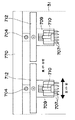
ユニット装置1001は、固定機構の一例として固定部1010と、移動機構の一例として移動部1020とを、ユニット装置1001における機台下面に夫々を備えており、これら固定部1010及び移動部1020の構造を模式的に示す説明図を図14(A)〜(B)に示す。
【0116】
図14(A)において、固定部1010は、例えば、方形状にフレームで形成されたユニット装置1001の機台下部のフレームの四隅の各々に固定された支柱昇降機構の一例であるエアシリンダ1011と、上記機台下部のフレームより下方に向かって昇降可能に各エアシリンダ1011に取り付けられた支柱の一例である丸棒状の支持脚1012、及び支持脚1012の下部先端部と係合可能な凹部1013aを上面に有し、ユニット装置1001の設置面の一例である床1005上に設置されている支柱受部の一例である円盤状の脚受部1013とを備えている。
【0117】
支持脚1012はその下方先端部に下向き円錐形状をしたテーパ部1012aを有しており、脚受部1013の凹部1013aの内側は、テーパ部1012aと係合するように同様にすり鉢形状となっている。また、脚受部1013の下面は床1005の上面との間において、摩擦抵抗を受け、床面上を滑り難くなるように形成されている。
【0118】
次に、図14(A)において、移動部1020は、上記機台下部のフレームの四隅の各々に固定された車輪の一例であるキャスター1021を備えている。
【0119】
このような固定部1010及び移動部1020によるユニット装置1001に対する固定動作及び移動動作について説明する。
【0120】
まず、図14(A)に示すように、4個のエアシリンダ1011により各支持脚1012が同時的に上昇されて、各支持脚1012のテーパ部1012aが各脚受部1013の凹部1013aから離された状態とされ、かつ4個のキャスター1021により、ユニット装置1001が支持されている状態とされることにより、ユニット装置1001はキャスター1021により移動可能な状態となる。
【0121】
次に、図14(B)に示すように、各エアシリンダ1011により各支持脚1012が同時的に下降されて、各支持脚1012のテーパ部1012aを各脚受部1013の凹部1013aに係合させ、さらに、各エアシリンダ1011により各支持脚1012を同時的に下降させて、各支持脚1012を予め定められている下降固定位置にまで伸ばして、ユニット装置1001を支持していた各キャスター1021を床1005上から同時的に浮き上がらせることにより、ユニット装置1001は固定部1010により固定された状態となる。
【0122】
このとき、ユニット装置1001に対して横方向に荷重が加えられるような場合であっても、脚受部1013にはユニット装置1001の自重が加わることとなるため、脚受部1013の下面と床面との間の摩擦抵抗は大きなものとなり、脚受部1013は床面上を動き難くなっているため、ユニット装置1001は安定されて固定されている。
【0123】
また、支持脚1012がその下方先端部に下向き円錐形状をしたテーパ部1012aを備え、脚受部1013の凹部1013aの内側がすり鉢形状となっていることにより、ユニット装置1001を固定部1010により固定するような場合において、支持脚1012のテーパ部1012aの位置が脚受部1013の凹部1013aの位置に対して多少の位置ずれがあるような場合であっても、夫々の形状により上記多少の位置ずれを補正しながら、支持脚1012のテーパ部1012aを脚受部1013の凹部1013aに円滑に係合させることができる。
【0124】
なお、ユニット装置1001の機台下面のフレームの四隅に固定部1010のエアシリンダ1011及び移動部1020のキャスター1021が備えられている場合について説明したが、上記フレームにバランスよく各エアシリンダ1011及び各キャスター1021が備えられてさえいれば、上記設置場所及び上記設置個数に限定されない。
【0125】
このようなユニット装置1001を複数備える実装基板生産装置1101において、ユニット装置1001の移動動作及び固定動作の手順を示す模式説明図を図15(A)〜(C)に示す。
【0126】
図15(A)において、幅2Wにより形成されている複数のユニット装置1001が、図示右側より順に、ユニット装置1001−1及び1001−2が隣接されて、ユニット装置1001−4及び1001−5が隣接されてそれぞれ固定部1010により床面に固定されて配置されており、ユニット装置1001−2と1001−4の間には、幅2Wを有する空間が設けられている。この空間にはユニット装置1001−3が設置可能なように、4個の脚受部1013が位置決めされて床面に配置されている。
【0127】
次に、図15(B)に示すように、上記幅2Wを有する空間にユニット装置1001−3を移動部1020のキャスター1021により移動させ、ユニット装置1001−3が備える4個の固定部1010における各支持脚1012のテーパ部1012aが、位置決めされ配置されている脚受部1013の凹部1013aと係合可能なように、ユニット装置1001−3をキャスター1021により微小移動させて、各支持脚1012のテーパ部1012aと脚受部1013の凹部1013aとの位置合わせを行う。
【0128】
その後、各固定部1010において、4個のエアシリンダ1011により、各支持脚1012を同時的に下降させて、各テーパ部1012aを各脚受部1013の凹部1013aに係合させ、さらに、各支持脚1012を上記下降固定位置まで下降させることにより、図15(C)に示すように、各キャスター1021を床1005上から浮き上がらせ、ユニット装置1001−3を各支持脚1012により支持させた状態とさせ、床1005に固定する。
【0129】
これにより、ユニット装置1001−1から1001−5までが、隣接して配置されて固定された状態となるとともに、各ユニット装置1001が備える搬送装置がそれぞれ同じ高さに位置されて、1つの搬送ラインが形成された実装基板生産装置が構成されることとなる。
【0130】
なお、各ユニット装置1001において、各支持脚1012の上記下降固定位置は、各エアシリンダ1011により、各支持脚1012が上記下降固定位置にまで下降された場合に、各ユニット装置1001間の各搬送装置が同じ高さとなるように、予め調整され設定されている。
【0131】
なお、各ユニット装置1001により構成された上記実装基板生産装置においては、上記において説明したように、各ユニット装置1001が備える移動部1020による移動動作、固定部1010による固定動作を組み合わせて行うことにより、各ユニット装置1001の配列変更やユニット装置の追加及び交換を行うことができる。
【0132】
次に、上記において説明したように実装基板生産装置を構成する各ユニット装置1001が、上記基準寸法の幅Wの整数倍の幅を有する第1ユニット装置1001aと、上記基準寸法の幅Wの2以上の整数倍の幅を有する第2ユニット装置1001bとを備えることにより、実装基板生産装置における各ユニット装置1001の機種入れ替えや、配置変更を行う場合における効果を以下に示す具体例を基に説明する。
【0133】
図16(A)〜(E)は、実装基板生産装置における各ユニット装置の配列を模式的に示した説明図である。まず、図16(A)において、実装基板生産装置1101aは、図示右側より左側へ順に、幅Wを有する印刷装置1003−1と、幅2Wを有する電子部品装着装置の一例であるチップ部品装着装置1001a−1と、幅2Wを有するチップ部品装着装置1001a−2と、及び幅4Wを有するリフロー装置1001b−1とを備えており、実装基板生産装置1101aにおける上記幅方向の全長は9Wとなっている。
【0134】
このような構成の実装基板生産装置1101aにおいて、実装される電子部品の種類の変更や生産される基板の種類の変更等に伴うユニット装置1001の機種入替えを行う場合、幅2Wのチップ部品装着装置1001a−2に代えて、幅3Wを有する電子部品装着装置の一例であるIC装着装置1001a−3を、幅4Wのリフロー装置1001b−1に代えて、幅3Wを有するリフロー装置1001b−2を設置することにより、図16(B)に示すように、機種の入替えを伴わない印刷装置1003−1及びチップ部品装着装置1001a−1の配置を変更することなく、実装基板生産装置1101aの全長9Wと同じ全長を有する実装基板生産装置1101bを構成することができる。
【0135】
また、実装基板生産装置1101aにおいて、上記のような機種入替えを行う場合における別の例として、幅2Wのチップ部品装着装置1001a−1に代えて、幅Wを有するチップ部品装着装置1001a−4及び幅Wを有するチップ部品装着装置1001a−5を、幅4Wのリフロー装置1001b−1に代えて、幅2Wを有するリフロー装置1001b−3及び幅2Wを有するリフロー装置1001b−4を設置することにより、図16(C)に示すように、機種の入替えを伴わない印刷装置1003−1及びチップ部品装着装置1001a−2の配置を変更することなく、実装基板生産装置1101aの全長9Wと同じ全長を有する実装基板生産装置1101cを構成することができる。
【0136】
また、図16(D)に示すように、実装基板生産装置1101dが、図示右側より左側へ順に、幅2Wを有する印刷装置1003−11と、幅2Wを有するチップ部品装着装置1001a−11と、幅2Wを有するチップ部品装着装置1001a−12と、及び幅2Wを有するリフロー装置1001b−11とを備えており、実装基板生産装置1101dにおいては、各ユニット装置1001が全て同じ幅2Wにて構成されている。
【0137】
このような実装基板生産装置1101dにおいて、例えば、チップ部品装着装置1001a−12のみを異なる機種であるIC装着装置に交換するような場合にあっては、IC装着装置として、チップ部品装着装置1001a−12と同じ幅2Wで構成されたIC装着装置1001a−13を用いることにより、図16(E)に示すように、実装基板生産装置1101dにおけるチップ部品装着装置1001a−12以外のユニット装置1001を移動することなく、IC装着装置1001a−13を設置することができ、実装基板生産装置1101eを構成することができる。
【0138】
また、図16(A)〜(C)までに示すように、実装基板生産装置が設置される床面上に、各ユニット装置1001が備える固定部1010の脚受部1013が、ユニット装置1001の幅の最小単位である基準寸法Wのピッチでもって予め設置されている場合にあっては、実装基板生産装置におけるユニット装置の配置変更作業や交換作業等が行われる場合において、ユニット装置の設置位置の位置決めを容易とすることができる。
【0139】
上記第2実施形態によれば、実装基板生産装置を構成している各ユニット装置1001が、従来における各作業装置のように、それぞれ個別の幅で形成されているのではなく、基準寸法の一例である幅Wの整数倍の幅若しくは幅Wの2以上の整数倍の幅で形成されているため、例えば、複数台配列されたユニット装置1001において、1台若しくは複数台のユニット装置1001を交換するような場合にあっては、当該1台若しくは複数台のユニット装置1001を移動させた後、当該1台若しくは複数台のユニット装置1001が配置されていた位置である空間に、その空間が有する幅、つまり上記幅Wの整数倍の幅と同じ寸法でユニット装置の幅の合計寸法が構成された1台若しくは複数台の新たなユニット装置1001を配置させることができる。従って、実装基板生産装置における1台若しくは複数台のユニット装置の配置変更作業又は交換作業等において、配置変更作業又は交換作業等が施されないユニット装置の配置への影響を無くすことができる又は少なくすることができ、ユニット装置の配置変更作業又は交換作業等を容易に行うことができる実装基板生産装置を提供することが可能となる。
【0140】
さらに、実装基板生産装置を構成する各ユニット装置が、各ユニット装置を移動可能に固定して配置させている固定部及び移動部を備えることにより、上記一定の幅Wの整数倍の幅若しくは一定の幅Wの2以上の整数倍の幅で形成されたユニット装置の固定作業及び移動作業を容易に行うことができ、ユニット装置の配置変更作業等を容易に行うことができる実装基板生産装置を提供することが可能となる。
【0141】
また、ユニット装置1001が備える固定部1010が、ユニット装置1001を支持して固定可能な支持脚1012を昇降させる機構として、エアシリンダ1011を備えることにより、各エアシリンダ1011を同時的に稼動させることによって各支持脚1012の同時的な昇降動作を容易に行うことができるため、ユニット装置1001の固定動作及び移動動作を容易にかつ安定して行うことができ、ユニット装置の配置変更作業等を容易にかつ円滑に行うことができる実装基板生産装置を提供することが可能となる。
【0142】
また、実装基板生産装置が設置される床面上に、各ユニット装置1001が備える固定部1010の脚受部1013が、ユニット装置1001の幅の最小単位である基準寸法Wのピッチでもって予め設置されている場合にあっては、実装基板生産装置におけるユニット装置の配置変更作業や交換作業等が行われる場合において、ユニット装置1001の設置位置の位置決めを容易とすることができる。
【0143】
なお、本発明は上記実施形態に限定されるものではなく、その他種々の態様で実施できる。例えば、本発明の第3実施形態にかかる実装基板生産装置を構成するユニット装置1050は、上記第2実施形態における実装基板生産装置を構成するユニット装置1001における固定部1010と異なる構造の固定部1060を備えており、その他の部分は、ユニット装置1001と同様であるため、この異なる部分である固定部1060についてのみ以下に説明する。
【0144】
図17(A)〜(B)にユニット装置1050がその機台下面に夫々備える固定機構の一例である固定部1060、及び移動機構の一例である移動部1020のそれぞれの構造を模式的に示す説明図を示す。
【0145】
図17(A)において、固定部1060は、例えば、方形状にフレームで形成されたユニット装置1050の機台下部のフレームの四隅の各々に固定された支柱昇降機構の一例であるナット部1061と、上記機台下部のフレームより下方に向かって昇降可能に各ナット部1061に螺合して取り付けられた支柱の一例であるねじ軸部1062、及びねじ軸部1062の下部先端部に取り付けられた支柱受部の一例である円盤状の軸受盤1063とを備えている。軸受盤1063の下面は、ユニット装置1050の設置面の一例である床1005の上面との間において、摩擦抵抗を受け、床面上を滑り難くなるように形成されている。
【0146】
図17(A)において、移動部1020は、上記第2実施形態の移動部1020と同じであり、上記機台下部のフレームの四隅の各々に固定された車輪の一例であるキャスター1021を備えている。
【0147】
このような固定部1060及び移動部1020によるユニット装置1005に対する固定動作及び移動動作について説明する。
【0148】
まず、図17(A)に示すように、4個のナット部1061と夫々螺合している各ねじ軸部1062が各ナット部1061に対して相対的かつ同時的に回転されることにより各ナット部1061と床1005との間において、各ねじ軸部1062が同時的に上昇されて、各ねじ軸部1062の先端部に取り付けられている軸受盤1063が床1005より離された状態とされ、かつ4個のキャスター1021により、ユニット装置1050が支持されている状態とされることにより、ユニット装置1050はキャスター1021により移動可能な状態となる。
【0149】
次に、図17(B)に示すように、各ナット部1061と夫々螺合している各ねじ軸部1062が各ナット部1061に対して相対的かつ同時的に回転されることにより各ナット部1061と床1005との間において、各ねじ軸部1062が同時的に下降されて、各ねじ軸部1062の先端部に取り付けられている軸受盤1063を床1005の上面に当接させ、さらに、各ねじ軸部1062を各ナット部1061に対して相対的かつ同時的に回転させることにより、各ナット部1061と床1005との間において、各ねじ軸部1062を同時的に下降させて、ユニット装置1050を支持していた各キャスター1021を床1005の上面から浮き上がらせることにより、ユニット装置1050は固定部1060により固定された状態となる。
【0150】
このとき、ユニット装置1050に対して横方向に荷重が加えられるような場合であっても、軸受盤1063にはユニット装置1005の自重が加わることとなるため、軸受盤1063の下面と床面との間の摩擦抵抗は大きなものとなり、軸受盤1063は床面上を動き難くなっているため、ユニット装置1050は安定されて固定されている。
【0151】
このようなユニット装置1050を複数備える実装基板生産装置において、ユニット装置1050の移動動作及び固定動作の手順については、上記第2実施形態と同様であるため説明を省略する。
【0152】
なお、各ユニット装置1050が、連設して配置されて固定された状態とされた場合において、各ユニット装置1050が備える搬送装置をそれぞれ同じ高さとするために、各ユニット装置1050における固定部1060にて、各ねじ軸部1062を各ナット部1061に対して相対的に回転させることにより、各搬送装置の高さ調整を行う。
【0153】
また、固定部1060において、軸受盤1063がねじ軸部1062の先端部に取り付けられている場合に代えて、上記第2実施形態における脚受部1013のように、軸受盤1063が床1005上に設置されており、ねじ軸部1062の下部先端部と係合可能な凹部をその上面に備えている場合であってもよい。
【0154】
上記第3実施形態によれば、上記第2実施形態による効果と同様に、実装基板生産装置を構成している各ユニット装置1001が、従来における各作業装置のように、それぞれ個別の幅で形成されているのではなく、基準寸法の一例である幅Wの整数倍の幅若しくは幅Wの2以上の整数倍の幅で形成されているため、例えば、複数台配列されたユニット装置1001において、1台若しくは複数台のユニット装置1001を交換するような場合にあっては、当該1台若しくは複数台のユニット装置1001を移動させた後、当該1台若しくは複数台のユニット装置1001が配置されていた位置である空間に、その空間が有する幅、つまり上記幅Wの整数倍の幅と同じ寸法でユニット装置の幅の合計寸法が構成された1台若しくは複数台の新たなユニット装置1001を配置させることができる。従って、実装基板生産装置における1台若しくは複数台のユニット装置の配置変更作業又は交換作業等において、配置変更作業又は交換作業等が施されないユニット装置の配置への影響を無くすことができる又は少なくすることができ、ユニット装置の配置変更作業又は交換作業等を容易に行うことができる実装基板生産装置を提供することが可能となる。
【0155】
さらに、実装基板生産装置を構成する各ユニット装置が、各ユニット装置を移動可能に固定して配置させている固定部及び移動部を備えることにより、上記基準寸法である幅Wの整数倍の幅若しくは幅Wの2以上の整数倍の幅で形成されたユニット装置の固定作業及び移動作業を容易に行うことができ、ユニット装置の配置変更作業等を容易に行うことができる実装基板生産装置を提供することが可能となる。
【0156】
さらに、付け加えて、上記第2実施形態のように固定部においてエアシリンダを用いるのではなく、ナット部とねじ軸部といった簡単な機構を用いて、ナット部に対してねじ軸部を相対的に正逆回転させることによりねじ軸部を昇降可能としているため、ユニット装置の製作コストを削減することが可能となる。
【0157】
本発明の上記第13態様によれば、実装基板生産装置を構成している各ユニット装置が、従来における各作業装置のように、それぞれ個別の幅で形成されているのではなく、上記実装基板生産装置が、上記各ユニット装置として、基板の搬送方向に沿って基準寸法の整数倍の寸法を有する第1ユニット装置、及び上記基準寸法の2以上の整数倍の寸法を有する第2ユニット装置を備えているため、例えば、複数台配列された上記ユニット装置において、1台若しくは複数台の上記ユニット装置を交換するような場合にあっては、当該1台若しくは複数台の上記ユニット装置を移動させた後、当該1台若しくは複数台のユニット装置が配置されていた位置である空間に、当該空間が有する上記搬送方向における寸法、つまり上記基準寸法の整数倍の寸法と同じ寸法で、上記ユニット装置の幅の合計寸法が構成された1台若しくは複数台の新たなユニット装置を配置させることができる。従って、実装基板生産装置における1台若しくは複数台のユニット装置の配置変更作業又は交換作業等において、上記配置変更作業又は上記交換作業等が施されないユニット装置の配置への影響を無くすことができる又は少なくすることができ、上記ユニット装置の配置変更作業又は交換作業等を容易に行うことができる実装基板生産装置を提供することが可能となる。
【0158】
本発明の上記第14態様又は上記第15態様によれば、上記第1態様による効果に付け加えて、上記実装基板生産装置を構成する上記各ユニット装置が、上記ユニット装置を移動可能に固定して配置させている固定機構及び移動機構を備えることにより、上記基準寸法の整数倍の寸法若しくは上記基準寸法の2以上の整数倍の寸法で形成された上記ユニット装置の固定作業及び移動作業を容易に行うことができ、上記ユニット装置の配置変更作業等を容易に行うことができる実装基板生産装置を提供することが可能となる。
【0159】
本発明の上記第16態様によれば、ユニット装置が備える固定機構が、上記ユニット装置を支持して固定可能な支柱を昇降させる支柱伸縮機構として、シリンダを備えることにより、上記各シリンダを同時的に稼動させることによって上記各支柱の同時的な昇降動作を容易に行うことができるため、上記ユニット装置の固定動作及び移動動作を容易にかつ安定して行うことができ、上記ユニット装置の配置変更作業等を容易にかつ円滑に行うことができる実装基板生産装置を提供することが可能となる。
【0160】
本発明の上記第17態様によれば、ユニット装置が備える固定機構が、ナット部とねじ軸部といった簡単な機構を用いることにより、ユニット装置の製作コストを削減することができ、上記ユニット装置の配置変更作業等を容易に行うことができる実装基板生産装置を安価に提供することが可能となる。
【0161】
本発明の上記第18態様によれば、ユニット装置に備えられる固定機構が、各支柱伸縮機構により伸ばされた各支柱の先端部と係合可能な凹部を有する支柱受部を備えることにより、上記ユニット装置の移動動作及び固定動作を行う場合において、予め上記ユニット装置の固定位置における設置面上に上記各支柱受部を設置しておくことができるため、上記ユニット装置の固定位置の位置決めを容易にすることができるとともに、上記ユニット装置を支持して固定する上記各支柱の先端部により設置面を傷つけることなく上記ユニット装置を固定することができ、上記ユニット装置の配置変更作業等を容易に行うことができる実装基板生産装置を提供することが可能となる。
【0162】
本発明の上記第19態様によれば、実装基板生産装置において用いられる実装基板生産装置用電子部品装着装置が、上記電子部品装着装置を移動可能に固定して配置させている固定機構及び移動機構を備えることにより、上記電子部品装着装置の固定作業及び移動作業を容易に行うことができ、上記電子部品装着装置の配置変更作業等を容易に行うことができる実装基板生産装置用電子部品装着装置を提供することが可能となる。
【0163】
(第4〜6実施形態)
本発明の第4〜6実施形態は、電子部品99を回路基板8上に装着する、上記第1〜第3実施形態にかかる電子部品装着装置の構造に関するものである。
【0164】
近年、電子部品実装においては電子部品を高速かつ正確に実装することが要求されている。
【0165】
以下、図19を参照しながら、従来の電子部品装着装置について説明する。図19は電子部品装着装置の全体概略図である。図19において、801は電子回路基板8を搬入・搬出する搬送部、803はX軸ボールネジ軸、804はY軸ボールネジ軸であり、この1本のX軸と2本のY軸から成るX−Yロボットにより部品供給部805より電子部品99を装吸着するノズル807及び電子回路基板8上に設けられた基板マーク808の位置を計測する基板認識カメラ810を電子回路基板8上の任意の位置へ位置決めする装置構成となっている。また、811は電子部品99の吸着姿勢を計測する部品認識カメラである。
【0166】
以上のように構成された電子部品装着装置について、以下その動作について説明する。まず、電子回路基板8は搬送部801により所定の位置へと搬入される。X−Yロボットはヘッド809に設けられた基板認識カメラ810を電子回路基板8上に設けられた基板マーク808上へ移動する。ここで基板認識カメラ810は電子回路基板8の位置を計測し、電子部品99の装着すべき位置を補正する。次にX−Yロボットは供給部805上へ移動し、ノズル807を降下させ、電子部品99を吸着した後、部品認識カメラ811上へ移動し、電子部品99の吸着姿勢を撮像して、補正を行い、電子部品99は電子回路基板8上へ装着される。
【0167】
しかしながら、上記構成の電子部品装着装置においては、次のような課題を有していた。
【0168】
まず、X−Yロボット型部品装着装置においては、上記説明及び図20に示すように、1本のX軸ボールネジ軸803と、その下方の両サイドに設けられた2本のY軸ボールネジ軸804から構成されており、2本のY軸ボールネジ軸804でX軸ボールネジ軸803を移動させる為、設備架台が大きくなってしまう設備構造であった。また、X軸ボールネジ軸803ではモータを設置する空間が必要となり、これも設備架台が大きくなる要因であった。
【0169】
さらに、図22に示したX−Yロボット型部品装着装置のX方向に一列もしくは複数列に配された複数ノズル807を有するヘッド809において基板認識カメラ810がノズル列X方向の延長線上に設置され、X方向での電子部品99の装吸着のストロークが小さいという課題を有していた。
【0170】
本発明の第4〜6実施形態は、上記従来の課題を解決するもので、面積生産性の向上を図ることのできる電子部品装着装置を提供することを目的とする。
【0171】
図19〜図26により本発明の実施の形態を示す。
【0172】
以下本発明の第4実施形態について、図を参照しながら説明する。
【0173】
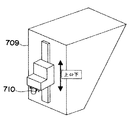
図21〜図24は本発明の第4実施形態を示すものであり、ヘッド部709を任意の位置へ移動させるX−Yロボットの構成図である。図21〜図24に示すように複数の電子部品99を装吸着する複数のノズル707を有する装着部及び認識部の一例としての基板認識カメラ710を有するヘッド部709を任意の位置へ移動させるX−Yロボットは、Y軸ボールネジ軸704及びX軸リニアモータ712から成り、このX−Yロボットは、装置天井770から吊下げられた天井吊下げ型に設けられている。具体的には、1本のY軸ボールネジ軸704が装置天井770に吊下げられ、Y軸ボールネジ軸704の下方に同じく1本のX軸リニアモータ712が設置された構成となっている。
【0174】
以上のように構成された第4実施形態の電子部品装着装置において、その動作について図21〜図24を用いて説明する。
【0175】
上記説明したように構成されたX−YロボットはX方向及びY方向に移動可能であり、Y方向については、Y軸方向移動装置の一例としてのY軸ボールネジ軸704により紙面に対し手前及び奥に移動可能である。また、X方向については、X軸方向移動装置の一例として、1本で吊下げられたY軸ボールネジ軸704の下方に設けられたX軸リニアモータ712により紙面の左右方向に移動可能である。ロボット全体としては任意の位置に対し、X軸リニアモータ712とY軸ボールネジ軸704がそれぞれ独立に移動し、目標とする任意の位置へ移動可能である。
【0176】
次に、本発明の第4実施形態の電子部品装着装置と従来の電子部品装着装置との違いについて図20及び図21〜図24を用いて説明する。図20は従来のX−Yロボットの構成図である。図20に示すように従来のX−Yロボットは1本のX軸ボールネジ軸803とその下方両サイドにX軸ボールネジ軸803に対し垂直に設けられた2本のY軸ボールネジ軸804とから構成され、Y方向の移動に対しては、X軸ボールネジ軸803が左右に設置された2本のY軸ボールネジ軸804上を移動することで、X軸ボールネジ軸に取り付けられたノズル807及び基板認識カメラ810を有するヘッド809を電子回路基板8上の装着すべき位置へ移動させる機構であった。これに対し、本発明の第4実施形態では図21〜図24及び上記説明にあるような構成及び動作の特徴を有しており、図20と図21〜図24を比較すると、従来の構成ではX−Yロボット全体でc+2bの施設幅を要していたのに対し、本発明の第4実施形態では両端にY軸ボールネジ軸が無いため施設幅がcのみで構成することができる。
【0177】
以上のように、第4実施形態によれば、X−Yロボットの構成について、Y軸方向移動装置が1本で天井吊下げ型に構成され、その下方にX軸方向移動装置を吊下げる構成を実施することにより、従来と比較し、設備架台幅を縮小することができる。
【0178】
また、第4実施の形態によれば、X軸方向移動装置としてリニアモータを備えることで、従来のボールネジ軸を備えることによるモータ部によるスペースを排除することができ、結果的に従来と比較し、設備架台幅を縮小することができる。さらに、設備幅が小さくなり、小さいサイズの基板を使用することにより、リニアモータをX軸方向移動装置として使用した天吊り型のX−Yロボットでは、X軸方向の中央付近でのたわみを低減させることができ、装着精度の向上をさらに図ることができる。すなわち、基板に電子部品を装着させる部品装着位置のほぼ真上にY軸方向移動装置を配置することによって、X軸方向の中央付近でのたわみを低減させることができ、電子部品の装着精度を高める構成とすることができる。従来は、Y軸方向移動装置が部品装着装置の両端に2本あり、その上にX軸方向移動装置が1本ある構成であったので、実際に作業をする位置では、X軸ロボットが撓んでおり、微小部品の装着が困難であった。これに対して、第4実施形態では、上記したように微小部品の装着を高精度で行うことができる。
【0179】
また、上記第4実施形態では、認識部の一例としての基板認識カメラ710を従来と異なる位置に配置している。
【0180】
すなわち、図21〜図24に加えて、図26は上記電子部品装着装置におけるヘッド部709の構成図であり、設備内に備えられた2つのヘッド部709を下方から見た模式図である。707は電子部品99を装吸着するノズル、710は電子回路基板8上に設けられた基板マーク(例えば図19の従来の基板マーク808)を撮像する基板認識カメラを示している。図26に示すようにヘッド部内部ではX方向に二列に配された複数ノズル707の前方に基板認識カメラ710が備えられた構成を有している。
【0181】
以上のように構成された第4実施形態の電子部品装着装置において、その動作について図21〜図24及び図26を用いて説明する。
【0182】
設備内に電子回路基板8が搬送された後、ヘッド部709は、X−Yロボットにより、例えば図26の下向きに電子回路基板8上に設けられた基板マーク上へ移動し、ヘッド部709内に備えられた基板認識カメラ710により基板マークを撮像し、電子回路基板8上への任意の位置への装着の為の補正を行なうものである。また、ヘッド部709は、X−Yロボットにより、図26の上向きに移動して図3の部品供給カセット5から部品99を吸着して上記電子回路基板8上への任意の位置への装着を行うことができる。
【0183】
次に、本発明の第4実施形態の電子部品装着装置と従来の電子部品装着装置との違いについて図25及び図26を用いて説明する。図25は従来のヘッド部内部の構成図である。図25に示すように従来の構成についてはヘッド部内部においてX方向に二列に配された複数ノズル807の延長線上に基板認識カメラ810が備えられており、設備内に配置される2つのヘッド部809両端間の幅Bに対し、電子部品を装吸着する際のストロークaが小さかった。これに対し、本発明の第4実施形態の電子部品装着装置は図26及び上記説明にあるように部品認識カメラ810をX方向に二列に配された複数ノズル807の前方に配置することで、同じ2つのヘッド部両端間の幅Bに対し、装吸着のストロークAを大きく取ることができる。
【0184】
実例として、ストローク(ヘッド部中心間距離)aを240mm、2つのヘッド両端間の幅をB450mmとするとき、第4実施形態では、吸着のストロークAは中央に対して両側に150mmずつ移動することができ、吸着のストロークAの合計は300mmとなる。これに対して、従来では、図25の右端のカメラの幅60mm分だけ移動することができず、従来の吸着のストロークは、300mm−60mm=240mmとなる。従って、(第4実施形態の吸着のストローク/従来の吸着のストローク)×100=(300/240)×100=125より、吸着のストロークは25%増すことになる。
【0185】
以上のように第4実施形態によれば、ヘッド部の構成について、ノズルの前方に基板認識カメラを備える構成を実施することにより、従来と比較し、ノズル配列方向言い換えればX方向での装吸着のストロークを拡大することができる。
【0186】
なお、上記様々な実施形態のうちの任意の実施形態を適宜組み合わせることにより、それぞれの有する効果を奏するようにすることができる。
【0187】
本発明は、添付図面を参照しながら好ましい実施形態に関連して充分に記載されているが、この技術の熟練した人々にとっては種々の変形や修正は明白である。そのような変形や修正は、添付した請求の範囲による本発明の範囲から外れない限りにおいて、その中に含まれると理解されるべきである。
【0188】
【発明の効果】
以上のように本発明によれば、電子部品装着装置において、まず、Y軸軸方向移動装置が天井吊下げ型に設置され、X軸軸方向移動装置がその下方に吊下げられた構成のX−Yロボットを備えることで、設備架台幅の縮小を図ることができる。
【0189】
また、X軸軸方向移動装置にはリニアモータを採用しているため、従来構成のボールネジ軸を採用することによるモータ部のスペースを削除し、設備架台幅の縮小を図ることができる。
【0190】
さらに、ノズルと電子回路基板上に設けられた基板マークを撮像する認識部としての光学撮像装置を有するヘッド部駆動装置において、X方向に一列もしくは複数列に配された複数ノズルX軸方向の両端の間のY軸方向の前方もしくは後方に上記光学撮像装置を配置することにより、電子部品装吸着ストロークの拡大を図ることができる。
【0191】
よって、電子部品装着装置における面積生産性の向上を図ることができる。すなわち、設備架台幅の縮小及び電子部品装吸着ストロークの拡大の面から面積生産性の向上を図ることができる。
【図面の簡単な説明】
【図1】 (A)は、本発明の第1実施形態にかかる実装基板生産装置の電子部品装着システムの斜視図であり、
(B)は、上記電子部品装着システムで電子部品が実装された基板の斜視図である。
【図2】 上記電子部品装着システム中の高速装着装置の斜視図である。
【図3】 図2にて上部カバーを透視した状態の上記高速装着装置を示す斜視図である。
【図4】 上記高速装着装置の正面図である。
【図5】 作業者が上記高速装着装置に対して作業する様子を示す図である。
【図6】 作業者が上記高速装着装置に対して作業する様子を示す図である。
【図7】 上記高速装着装置の装着機構の底面図である。
【図8】 上記高速装着装置の上記装着機構よりも下方の様子を示す平面図である。
【図9】 上記高速装着装置の側面図である。
【図10】 上記高速装着装置の保護カバーを開いた様子を示す図である。
【図11】 上記高速装着装置の操作盤をヘッド部から待避させた様子を示す図である。
【図12】 従来の電子部品装着システムを示す斜視図である。
【図13】 本発明の第2実施形態にかかる実装基板生産装置の斜視図である。
【図14】 (A)、(B)は、それぞれ、上記第2実施形態におけるユニット装置の固定部及び移動部の構造の模式説明図である。
【図15】 (A)、(B)、(C)は、それぞれ、上記第2実施形態におけるユニット装置の移動動作及び固定動作の模式説明図である。
【図16】 (A)、(B)、(C)、(D)、(E)は、それぞれ、上記第2実施形態の実装基板生産装置におけるユニット装置の配列の模式平面図である。
【図17】 (A)、(B)は、それぞれ、本発明の第3実施形態にかかる実装基板生産装置におけるユニット装置の固定部及び移動部の構造の模式説明図である。
【図18】 従来における実装基板生産装置の斜視図である。
【図19】 従来の電子部品装着装置の全体概略斜視図である。
【図20】 電子部品装着装置における従来のX−Yロボット構成図である。
【図21】 本発明の第4実施形態における電子部品装着装置のX−Yロボットの詳細な構成図である。
【図22】 本発明の第4実施形態における電子部品装着装置のX−Yロボットの概略構成図である。
【図23】 本発明の第4実施形態における電子部品装着装置のX−Yロボットに支持されるヘッド部の、ノズルを省略した状態での概略斜視図である。
【図24】 本発明の第4実施形態を第1実施形態の電子部品装着装置に適用した具体例のX−Yロボット構成図である。
【図25】 電子部品装着装置における従来のヘッド部内部構成図である。
【図26】 本発明の第4実施形態における図24の電子部品装着装置のヘッド部内部構成図である。
【符号の説明】
1…電子部品装着システム、5…部品カセット、6…制御部、8…基板、21…高速装着装置、22…多機能装着装置、31…上部カバー、41…ヘッド部、42,43…駆動機構、99…電子部品、311…保護カバー、313…ヒンジ、331…ディスプレイ、334…ヒンジ、341…搬送レール、342…搬送駆動部、401…移動領域、704…Y軸ボールネジ軸、709…ヘッド部、710…基板認識カメラ、712…X軸リニアモータ、770…装置天井、1001…ユニット装置、1001a…第1ユニット装置、1001b…第2ユニット装置、1005…床、1010…固定部、1011…エアシリンダ、1012…支持脚、1012a…テーパ部、1013…脚受部、1013a…凹部、1020…移動部、1021…キャスター、1050…ユニット装置、1060…固定部、1061…ナット部、1062…ねじ軸部、1063…軸受盤、1101…実装基板生産装置、1110…印刷装置、1120…電子部品装着装置、1121…電子部品装着装置、1122…電子部品装着装置、1130…リフロー装置、1140…搬送ライン。[0001]
BACKGROUND OF THE INVENTION
The present invention relates to an electronic component mounting apparatus and a mounting board production apparatus for mounting electronic components on a substrate.
[0002]
[Prior art]
Conventionally, when an electronic component is mounted on a substrate such as a printed circuit board, a step of printing a cream-like solder paste on the substrate, a step of mounting the electronic component on the printed solder paste, and the electronic component are mounted The substrate is heated and cooled to solidify the solder, and the electronic component is fixed to the substrate.
[0003]
FIG. 12 is a perspective view showing a configuration of an electronic component mounting system 9 for mounting an electronic component on a substrate in a conventional mounting system for mounting the electronic component on the substrate. In the electronic component mounting system 9, the board on which the solder paste is printed is carried in from the direction indicated by the
[0004]
In the electronic component mounting system 9 shown in FIG. 12, three high-
[0005]
[Problems to be solved by the invention]
By the way, the electronic component mounting system 9 shown in FIG. 12 is designed so that electronic components can be mounted on a large substrate. On the other hand, with the widespread use of mobile terminals including mobile phones, miniaturization of substrates incorporated in mobile terminals has been promoted.
[0006]
Therefore, in order to efficiently mount electronic components on a substrate for a portable terminal using the electronic component mounting system 9, it is necessary to form a number of portable terminal circuits on a single substrate to be transported.
[0007]
However, with the diversification of mobile terminals, there is a growing demand for production (mounting) of various types of substrates, and the electronic component mounting system 9 shown in FIG. 12 is used for mounting electronic components on mobile terminal substrates. The configuration is not necessarily suitable.
[0008]
Accordingly, an object of the present invention is to provide an electronic component mounting apparatus and a mounting board production apparatus suitable for manufacturing a small board.
[0009]
[Means for Solving the Problems]
In order to achieve the above object, the present invention is configured as follows.
[0022]
According to the first aspect of the present invention, the mounting operation unit for mounting the electronic component by interposing the solder on the substrate, and the mounting of the electronic component by reflowing the solder to fix the electronic component on the substrate are produced. A mounting board production apparatus for producing the mounting board from the board while transporting the board to the mounting work part and the reflow working part.
The mounting board production apparatus is
The apparatus has the mounting work section, and the substantial device width along the substrate transport direction is a dimension that is an integral multiple of one reference dimension selected from the range of 270 mm to 330 mm, and a dimension of 450 mm to 1000 mm. A plurality of first unit devicesAnd,
A second unit device having the reflow working unit and having a substantial device width along the transport direction of the substrate being an integral multiple of 2 or more of the reference sizeWhen,
With
Each of the first unit device and the second unit device are connected along the transport direction and fixed to be movable.And
The first unit device is an electronic component mounting device for mounting the electronic component on the substrate.
The electronic component mounting apparatus is
An electronic component supply unit for supplying the electronic component;
A transport unit capable of transporting the substrate in the transport direction from the board standby position to the component mounting position, and further from the component mounting position to the outside of the component mounting position;
A head unit for mounting the electronic component of the electronic component supply unit on a substrate;
A drive unit for moving the head unit between the electronic component supply unit and the substrate;
A protective cover provided on the front surface of the electronic component mounting device so as to be rotatable by a first hinge;
An operation panel provided between the protective cover and the head portion and rotatably provided by a second hinge;
A mounting board production apparatus comprisingI will provide a.
According to a second aspect of the invention,The first hinge is provided at an upper end of the electronic component mounting device,
The second hinge is provided at the upper end of the operation panel.A mounting board production apparatus according to a first aspect is provided.
[0023]
According to a third aspect of the invention,The operation panel includes a display and operation buttons.A mounting board production apparatus according to the first or second aspect is provided.
[0024]
According to a fourth aspect of the present invention,The operation panel is any one of the first to third aspects provided in the electronic component mounting apparatus.The mounting board production apparatus described in 1. is provided.
[0025]
According to a fifth aspect of the present invention,The substantial device width of the electronic component mounting device is any one of the first to fourth aspects, which is the width of the frame of the electronic component mounting device or the width of the protective cover.The mounting board production apparatus described in 1. is provided.
[0026]
First of the present invention6According to the aspect, the support column is a screw shaft portion, the support column lifting mechanism is a nut portion screwed to the screw shaft portion, and the screw shaft portion is relatively forward and backward relative to the nut portion. By rotating the first column, the column attached to the column lifting mechanism is moved up and down.4The mounting board production apparatus according to the aspect is provided.
[0027]
First of the present invention7According to the aspect, the fixing mechanism further includes a column receiving portion that has a recess that can be engaged with the tip end portion of the column that is lowered by the column lifting mechanism and that is installed on the installation surface.4The mounting board production apparatus according to the aspect is provided.
[0033]
DETAILED DESCRIPTION OF THE INVENTION
Before continuing the description of the present invention, the same parts are denoted by the same reference numerals in the accompanying drawings.
[0034]
Embodiments according to the present invention will be described below in detail with reference to the drawings.
[0035]
(First embodiment)
FIG. 1A is a perspective view showing an external appearance of an electronic
[0036]
The electronic
[0037]
The
[0038]
The
[0039]
FIG. 2 is an external perspective view showing the front, right side, and plane of the high-
[0040]
The high-
[0041]
Between the
[0042]
FIG. 3 is a perspective view showing the internal structure of the high-
[0043]
The pair of
[0044]
A control unit 6 for controlling the mounting
[0045]
In the high-
[0046]
The high-
[0047]
Specifically, by handling a small substrate, a loss caused by discarding one substrate can be suppressed more than a large substrate (for example, a square substrate having a side of 250 mm or more). Further, by reducing the size of the high-
[0048]
In addition, by installing a large number of lines on the site of the same area, it is possible to suppress a decrease in production capacity when one line stops. Thus, a new added value can be obtained by using the small high-
[0049]
For the above reasons, the high-
[0050]
As shown in FIG. 4, when the width of the apparatus (that is, the substantial apparatus width with respect to the conveying direction) is AW and the height of the apparatus is H as viewed from the front, the apparatus is downsized (more precisely, the occupied area is reduced). ), The height H must be increased. However, as shown in FIG. 5, a person can perform work such as maintenance, initial adjustment, and driving operation of the apparatus. That is, the height MH considering workability is usually about 2000 mm. It is preferable to limit the height H to about 2000 mm. In view of safety, the height H of the apparatus is preferably limited to about 2000 mm from the necessity of reaching out without using a pedestal or the like. From such a viewpoint, the height of the apparatus is about 1300 to 2000 mm.
[0051]
By the way, when newly installing the high-
[0052]
[Expression 1]
H ・ tan20 ° <AW
[0053]
As a result, it can be concluded that when the height H is about 1300 mm, the width AW needs to be at least 450 mm, and when the height H is about 2000 mm, the width AW needs at least 600 mm. For this reason, even if the apparatus is tilted when the apparatus is installed, it is possible to return the posture without falling down, and it is possible to reduce damage and load generated in the apparatus itself.
On the other hand, as shown in FIG. 6, when a person performs an operation or work while facing the high-
[0054]
Further, when one of the plurality of high-
[0055]
From the above, from the viewpoint of ergonomics or from the viewpoint of workability, the width AW of the high-
[0056]
Of course, the larger the width AW of the device, the more stable the posture of the device and the larger the gap generated when the device is removed. However, when the size of the apparatus is increased, as described above, the switching operation of the substrate types and the replacement operation of the devices become large, which is not preferable from the viewpoint of handling various types of small substrates. Further, when the device width AW becomes too large, it is necessary to move a person when performing an operation or a confirmation operation on one device. Therefore, it is preferable that the width AW of the apparatus is suppressed to 1000 mm or less, which is a width MW2 that allows a person to work while spreading both arms.
[0057]
As described above, it is preferable that the width is 450 mm or more and 1000 mm or less, and more preferably about 600 mm, for the mounting device dedicated to the small substrate. Therefore, the high-
[0058]
The width AW of the device refers to a substantial width, and does not include protrusions or attached members present on the outer periphery of the device. Specifically, as shown in FIG. 3, when the mounting
[0059]
FIG. 7 is a view showing the two mounting
[0060]
In addition, each
[0061]
As shown in FIG. 7, the moving
[0062]
In the high-
[0063]
Further, in the high-
[0064]
Further, the length of one side of the quadrangle of the
[0065]
FIG. 8 is a plan view showing a configuration below the
[0066]
The
[0067]
Normally, when downsizing the apparatus, various types of
[0068]
7 and 8, an area denoted by
[0069]
When the
[0070]
By the operation described above, the mounting
[0071]
Next, a state where a plurality of high-
[0072]
As shown in FIG. 8, the gap between the high-
[0073]
In general, the distance between conventional mounting apparatuses has been such a length that an operator can remove a substrate (except when a large substrate is handled in particular). That is, the distance between the apparatuses has been set longer than the length of the substrate parallel to the transport direction. Such a setting is intended to make it possible to remove a poorly mounted substrate as needed immediately after it is unloaded from the apparatus.
[0074]
On the other hand, in the high-
[0075]
Furthermore, since the length of the mounting
[0076]
Next, the
[0077]
As described above, in the high-
[0078]
As shown in FIG. 2, the
[0079]
However, in the state shown in FIG. 10, although work can be performed on the lower side of the
[0080]
Therefore, in the high-
[0081]
The first embodiment according to the present invention has been described above. However, the present invention is not limited to the above embodiment, and various modifications can be made.
[0082]
For example, in the above description, the downsizing of the high-
[0083]
In the first embodiment, the
[0084]
In the first embodiment, the optimum design is performed by arranging two
[0085]
In the first embodiment, the
[0086]
In the first embodiment, it has been described that the distance between the mounting devices is equal to or less than the substrate width in the transport direction. However, the distance between the devices does not include unnecessary protrusions or additional configurations on the outer periphery of the device. . In the electronic
[0087]
Therefore, the distance between the devices refers to the distance in the vicinity of the transfer position of the
[0088]
Of course, depending on the device, there may be a case where the cover does not exist. Even in this case, since the apparatus is generally surrounded by the frame, the distance between the apparatuses can be defined as the distance between the frames near the position where the
[0089]
In the first embodiment, the
[0090]
Further, the
[0091]
According to the first to seventh aspects of the present invention, the electronic component mounting apparatus can be appropriately downsized.
[0092]
Further, according to the second aspect of the present invention, the electronic component mounting apparatus can be further downsized. According to the third aspect of the present invention, the configuration of the downsized electronic component mounting apparatus can be appropriately configured. Can do anything.
[0093]
In addition, according to the fourth aspect of the present invention, it is possible to reduce the size of the electronic component mounting apparatus appropriate for the size of the handling substrate.
[0094]
Further, according to the fifth aspect of the present invention, the movement control of the head part can be easily performed, and according to the sixth aspect of the present invention, the movement control of the head part can be more easily performed.
[0095]
Moreover, according to the 7th aspect of this invention, an electronic component mounting apparatus and an operator can be protected by a cover.
[0096]
According to the eighth to tenth aspects of the present invention, it is possible to reduce the size of the entire mounting board production apparatus, particularly an electronic component mounting system including a plurality of component mounting apparatuses.
[0097]
Further, according to the ninth aspect of the present invention, it is possible to reduce the substantial occupied area of the entire mounting board production apparatus, in particular, an electronic component mounting system including a plurality of component mounting apparatuses.
[0098]
Moreover, according to the 10th aspect of this invention, an electronic component mounting apparatus and an operator can be protected by a cover.
[0099]
According to the eleventh and twelfth aspects of the present invention, it is possible to easily perform work on the rear side of the display.
[0100]
Further, according to the twelfth aspect of the present invention, the display can be retracted with a simple mechanism.
[0101]
(Second and third embodiments)
In the second and third embodiments of the present invention, a mounting operation unit that mounts a plurality of electronic components by interposing solder on the substrate, and a reflow operation that reflows the solder and fixes the electronic components on the substrate. And a mounting substrate production apparatus for producing a plurality of mounting substrates from the plurality of substrates while transporting the plurality of substrates to the mounting operation unit and the reflow operation unit.
[0102]
Conventionally, this type of mounting board production apparatus has various structures. For example, as shown in FIG. 18, the conventional mounting
[0103]
In FIG. 18, the mounting
[0104]
In the mounting
[0105]
However, in the case of the structure described above, when the type of mounting board to be produced is switched, for example, the number of electronic components to be mounted may increase to a large number. Therefore, it is necessary to newly add an electronic component mounting apparatus for mounting the increased electronic components in the mounting
[0106]
Further, since each of the above-mentioned working devices constituting the mounting
[0107]
Accordingly, an object of the present invention is to solve the above-described problem, and includes a plurality of unit devices that perform a predetermined operation on a substrate, and produces a mounting substrate in which an electronic component is mounted on the substrate. In the apparatus, one of the unit devices used in the mounting substrate production apparatus and the mounting substrate production apparatus that facilitates replacement, movement, and fixing operations of the respective unit devices and facilitates the arrangement change of the respective unit devices. An object is to provide an electronic component mounting apparatus for a mounting board production apparatus.
[0108]
Embodiments according to the present invention will be described below in detail with reference to the drawings.
[0109]
As shown in FIG. 13, the mounting
[0110]
Each of the unit devices includes a transfer device for transferring a substrate, and is installed adjacent to each other so that a plurality of substrates can be transferred from the
[0111]
In such a mounted
[0112]
Further, as shown in FIG. 13, each of the
[0113]
Note that the
[0114]
Next, a description will be given of a fixing mechanism and a moving mechanism provided in a unit device that fixes and arranges each of the
[0115]
The
[0116]
In FIG. 14A, a fixed
[0117]
The
[0118]
Next, in FIG. 14A, the moving
[0119]
The fixing operation and moving operation with respect to the
[0120]
First, as shown in FIG. 14A, the
[0121]
Next, as shown in FIG. 14B, the
[0122]
At this time, even if a load is applied to the
[0123]
Further, the
[0124]
In addition, although the case where the
[0125]
FIGS. 15A to 15C are schematic explanatory views showing the procedure of the moving operation and the fixing operation of the
[0126]
In FIG. 15A, a plurality of
[0127]
Next, as shown in FIG. 15B, the unit device 1001-3 is moved to the space having the
[0128]
Thereafter, in each fixing
[0129]
As a result, the unit devices 1001-1 to 1001-5 are arranged adjacently and fixed, and the transport devices included in each
[0130]
In each
[0131]
In the mounting board production apparatus configured by each
[0132]
Next, as described above, each
[0133]
16A to 16E are explanatory views schematically showing the arrangement of the unit devices in the mounting board production apparatus. First, in FIG. 16A, a mounting
[0134]
In the mounting
[0135]
As another example in the case where the above-described model change is performed in the mounting
[0136]
Further, as shown in FIG. 16D, the mounting
[0137]
In such a mounting
[0138]
Further, as shown in FIGS. 16A to 16C, the
[0139]
According to the second embodiment, the
[0140]
Further, each unit device constituting the mounting board production apparatus includes a fixed part and a moving part that are fixedly arranged so that each unit apparatus can be moved, so that a width that is an integral multiple of the constant width W or a constant value. A mounting substrate production apparatus that can easily perform a fixing operation and a moving operation of a unit device formed with a width that is an integer multiple of 2 or more of the width W of the unit, and can easily perform an arrangement changing operation of the unit device. It becomes possible to provide.
[0141]
In addition, the
[0142]
In addition, the
[0143]
In addition, this invention is not limited to the said embodiment, It can implement with another various aspect. For example, the
[0144]
FIGS. 17A to 17B schematically show structures of a
[0145]
In FIG. 17A, the fixed
[0146]
In FIG. 17A, the moving
[0147]
A fixing operation and a moving operation with respect to the
[0148]
First, as shown in FIG. 17A, each
[0149]
Next, as shown in FIG. 17 (B), each
[0150]
At this time, even if a load is applied to the
[0151]
In the mounting board production apparatus including a plurality of
[0152]
In addition, when each
[0153]
Further, in the fixed
[0154]
According to the third embodiment, similarly to the effect of the second embodiment, each
[0155]
Further, each unit device constituting the mounting board production apparatus includes a fixed portion and a moving portion that are fixedly arranged so that each unit device can be moved, and thereby a width that is an integral multiple of the width W that is the reference dimension. Alternatively, there is provided a mounting board production apparatus that can easily perform a fixing operation and a moving operation of a unit device formed with a width that is an integer multiple of 2 or more of the width W, and can easily perform an arrangement changing operation of the unit device. It becomes possible to provide.
[0156]
In addition, instead of using an air cylinder in the fixed portion as in the second embodiment, a simple mechanism such as a nut portion and a screw shaft portion is used to move the screw shaft portion relative to the nut portion. Since the screw shaft portion can be moved up and down by rotating forward and backward, it is possible to reduce the manufacturing cost of the unit device.
[0157]
According to the thirteenth aspect of the present invention, each unit device constituting the mounting board production apparatus is not formed with an individual width as in each of the conventional work apparatuses, but the above mounting board. The production apparatus includes a first unit device having a dimension that is an integral multiple of a reference dimension along the substrate transport direction, and a second unit device having a dimension that is an integer multiple of 2 or more of the reference dimension, as each unit device. Therefore, for example, in the case where one or a plurality of the unit devices are replaced in the unit devices arranged in a plurality, the one or a plurality of the unit devices are moved. After that, in the space where the one or a plurality of unit devices are arranged, the dimension of the space in the transport direction, that is, an integer of the reference dimension In the same dimensions as can be arranged on the total dimension
[0158]
According to the fourteenth aspect or the fifteenth aspect of the present invention, in addition to the effect of the first aspect, each unit device constituting the mounting board production apparatus fixes the unit device to be movable. By providing the fixing mechanism and the moving mechanism that are arranged, the fixing operation and the moving operation of the unit device formed with an integral multiple of the reference dimension or an integral multiple of two or more of the reference dimension can be easily performed. Therefore, it is possible to provide a mounting board production apparatus that can easily perform the arrangement changing operation of the unit apparatus.
[0159]
According to the sixteenth aspect of the present invention, the fixing mechanism provided in the unit device includes a cylinder as a column extending / contracting mechanism that lifts and lowers the column that can be fixed by supporting the unit device. Since the simultaneous elevating operation of the respective columns can be easily performed by operating the unit device, the fixing operation and the moving operation of the unit device can be easily and stably performed, and the arrangement of the unit device can be changed. It is possible to provide a mounting board production apparatus that can easily and smoothly perform operations and the like.
[0160]
According to the seventeenth aspect of the present invention, since the fixing mechanism provided in the unit device uses a simple mechanism such as a nut portion and a screw shaft portion, the manufacturing cost of the unit device can be reduced. It is possible to provide a mounting board production apparatus that can easily perform an arrangement changing operation and the like at a low cost.
[0161]
According to the eighteenth aspect of the present invention, the fixing mechanism provided in the unit device includes the column receiving portion having a recess that can be engaged with the tip end portion of each column extended by each column expansion / contraction mechanism. When performing the moving operation and the fixing operation of the unit device, since each of the column receiving portions can be installed in advance on the installation surface at the fixing position of the unit device, it is easy to position the fixing position of the unit device. The unit device can be fixed without damaging the installation surface by the tip portions of the support columns that support and fix the unit device, and the arrangement of the unit device can be easily changed. It is possible to provide a mounting board production apparatus that can be performed.
[0162]
According to the nineteenth aspect of the present invention, the electronic component mounting apparatus for a mounting board production apparatus used in the mounting board production apparatus fixes and arranges the electronic component mounting apparatus so as to be movable. By providing the electronic component mounting apparatus, the electronic component mounting apparatus can be easily fixed and moved, and the electronic component mounting apparatus can be easily repositioned. Can be provided.
[0163]
(Fourth to sixth embodiments)
4th-6th Embodiment of this invention is related with the structure of the electronic component mounting apparatus concerning the said 1st-3rd embodiment which mounts the
[0164]
In recent years, in electronic component mounting, it is required to mount electronic components at high speed and accurately.
[0165]
Hereinafter, a conventional electronic component mounting apparatus will be described with reference to FIG. FIG. 19 is an overall schematic diagram of the electronic component mounting apparatus. In FIG. 19,
[0166]
The operation of the electronic component mounting apparatus configured as described above will be described below. First, the
[0167]
However, the electronic component mounting apparatus having the above configuration has the following problems.
[0168]
First, in the XY robot type component mounting apparatus, as shown in the above description and FIG. 20, one X-axis
[0169]
Further, in the
[0170]
The fourth to sixth embodiments of the present invention solve the above-described conventional problems, and an object thereof is to provide an electronic component mounting apparatus capable of improving the area productivity.
[0171]
19 to 26 show an embodiment of the present invention.
[0172]
A fourth embodiment of the present invention will be described below with reference to the drawings.
[0173]
FIGS. 21 to 24 show a fourth embodiment of the present invention, and are configuration diagrams of an XY robot that moves the
[0174]
The operation of the electronic component mounting apparatus according to the fourth embodiment configured as described above will be described with reference to FIGS.
[0175]
The XY robot configured as described above can move in the X direction and the Y direction. In the Y direction, the Y-axis
[0176]
Next, differences between the electronic component mounting apparatus according to the fourth embodiment of the present invention and the conventional electronic component mounting apparatus will be described with reference to FIGS. 20 and 21 to 24. FIG. 20 is a configuration diagram of a conventional XY robot. As shown in FIG. 20, the conventional XY robot is composed of one X-axis
[0177]
As described above, according to the fourth embodiment, with regard to the configuration of the XY robot, one Y-axis direction moving device is configured as a ceiling-suspended type, and the X-axis direction moving device is suspended below the Y-axis direction moving device. By implementing this, the installation stand width can be reduced as compared with the conventional case.
[0178]
Further, according to the fourth embodiment, by providing the linear motor as the X-axis direction moving device, it is possible to eliminate the space by the motor unit due to the provision of the conventional ball screw shaft. The equipment rack width can be reduced. Furthermore, the equipment width is reduced, and by using a small-sized substrate, a ceiling-suspended XY robot that uses a linear motor as the X-axis direction moving device reduces deflection near the center in the X-axis direction. The mounting accuracy can be further improved. In other words, by arranging the Y-axis direction moving device almost directly above the component mounting position for mounting the electronic component on the board, the deflection near the center in the X-axis direction can be reduced, and the mounting accuracy of the electronic component can be increased. It can be set as the structure which raises. Conventionally, there are two Y-axis direction moving devices at both ends of the component mounting device, and one X-axis direction moving device on the two, so that the X-axis robot is flexed at the actual work position. Therefore, it was difficult to mount minute parts. On the other hand, in the fourth embodiment, as described above, it is possible to mount the minute parts with high accuracy.
[0179]
Moreover, in the said 4th Embodiment, the board |
[0180]
That is, in addition to FIGS. 21 to 24, FIG. 26 is a configuration diagram of the
[0181]
The operation of the electronic component mounting apparatus according to the fourth embodiment configured as described above will be described with reference to FIGS.
[0182]
After the
[0183]
Next, differences between the electronic component mounting apparatus according to the fourth embodiment of the present invention and the conventional electronic component mounting apparatus will be described with reference to FIGS. 25 and 26. FIG. FIG. 25 is a configuration diagram of the inside of a conventional head unit. As shown in FIG. 25, in the conventional configuration, a
[0184]
As an example, when the stroke (distance between the head centers) is 240 mm and the width between the two head ends is B450 mm, in the fourth embodiment, the suction stroke A moves 150 mm to both sides with respect to the center. The total of the suction stroke A is 300 mm. On the other hand, in the related art, the camera cannot move by the width of 60 mm of the right end camera in FIG. 25, and the conventional suction stroke is 300 mm−60 mm = 240 mm. Accordingly, the suction stroke is increased by 25% from (the suction stroke of the fourth embodiment / the conventional suction stroke) × 100 = (300/240) × 100 = 125.
[0185]
As described above, according to the fourth embodiment, the configuration of the head unit is provided with the substrate recognition camera in front of the nozzles, so that compared with the conventional case, the nozzle arrangement direction, in other words, the X-direction suction / adsorption The stroke can be enlarged.
[0186]
It is to be noted that, by appropriately combining arbitrary embodiments of the various embodiments described above, the effects possessed by them can be produced.
[0187]
Although the present invention has been fully described in connection with preferred embodiments with reference to the accompanying drawings, various variations and modifications will be apparent to those skilled in the art. Such changes and modifications are to be understood as being included therein, so long as they do not depart from the scope of the present invention according to the appended claims.
[0188]
【The invention's effect】
As described above, according to the present invention, in the electronic component mounting apparatus, first, the X-axis direction moving device is installed in the ceiling hanging mold, and the X-axis axial direction moving device is suspended below the X-axis. By providing the -Y robot, the equipment rack width can be reduced.
[0189]
In addition, since a linear motor is employed in the X-axis axial direction moving device, the space of the motor unit can be eliminated by adopting a ball screw shaft having a conventional configuration, and the equipment rack width can be reduced.
[0190]
Furthermore, in the head unit driving device having an optical imaging device as a recognition unit that images a nozzle and a board mark provided on the electronic circuit board, both ends of the plurality of nozzles in the X-axis direction arranged in one or more rows in the X direction By disposing the optical imaging device in the front or rear in the Y-axis direction between them, the electronic component mounting stroke can be expanded.
[0191]
Therefore, the area productivity in the electronic component mounting apparatus can be improved. That is, the area productivity can be improved from the viewpoint of reducing the width of the installation base and increasing the suction stroke of the electronic component.
[Brief description of the drawings]
FIG. 1A is a perspective view of an electronic component mounting system of a mounting board production apparatus according to a first embodiment of the present invention;
(B) is a perspective view of a substrate on which electronic components are mounted in the electronic component mounting system.
FIG. 2 is a perspective view of a high-speed mounting device in the electronic component mounting system.
FIG. 3 is a perspective view showing the high-speed mounting device in a state where the upper cover is seen through in FIG. 2;
FIG. 4 is a front view of the high-speed mounting device.
FIG. 5 is a diagram showing how an operator works on the high-speed mounting device.
FIG. 6 is a diagram showing how an operator works on the high-speed mounting device.
FIG. 7 is a bottom view of the mounting mechanism of the high-speed mounting device.
FIG. 8 is a plan view showing a state below the mounting mechanism of the high-speed mounting device.
FIG. 9 is a side view of the high-speed mounting device.
FIG. 10 is a view showing a state where a protective cover of the high-speed mounting device is opened.
FIG. 11 is a diagram illustrating a state where the operation panel of the high-speed mounting device is retracted from the head unit.
FIG. 12 is a perspective view showing a conventional electronic component mounting system.
FIG. 13 is a perspective view of a mounting board production apparatus according to a second embodiment of the present invention.
FIGS. 14A and 14B are schematic explanatory views of the structures of the fixed portion and the moving portion of the unit device in the second embodiment, respectively.
FIGS. 15A, 15B, and 15C are schematic explanatory views of a moving operation and a fixing operation of the unit device in the second embodiment, respectively.
16A, 16B, 16C, 16D, and 16E are schematic plan views of arrangements of unit devices in the mounting board production apparatus of the second embodiment.
FIGS. 17A and 17B are schematic explanatory views of the structures of a fixed part and a moving part of a unit device in a mounting board production apparatus according to a third embodiment of the present invention, respectively.
FIG. 18 is a perspective view of a conventional mounting board production apparatus.
FIG. 19 is an overall schematic perspective view of a conventional electronic component mounting apparatus.
FIG. 20 is a configuration diagram of a conventional XY robot in an electronic component mounting apparatus.
FIG. 21 is a detailed configuration diagram of an XY robot of an electronic component mounting apparatus according to a fourth embodiment of the present invention.
FIG. 22 is a schematic configuration diagram of an XY robot of an electronic component mounting apparatus according to a fourth embodiment of the present invention.
FIG. 23 is a schematic perspective view of the head unit supported by the XY robot of the electronic component mounting apparatus according to the fourth embodiment of the present invention with the nozzle omitted.
FIG. 24 is an XY robot configuration diagram of a specific example in which the fourth embodiment of the present invention is applied to the electronic component mounting apparatus of the first embodiment.
FIG. 25 is a diagram showing the internal configuration of a conventional head unit in the electronic component mounting apparatus.
FIG. 26 is an internal configuration diagram of a head part of the electronic component mounting apparatus of FIG. 24 in the fourth embodiment of the present invention.
[Explanation of symbols]
DESCRIPTION OF
Claims (5)
上記実装基板生産装置は、
上記装着作業部を有し、かつ上記基板の搬送方向沿いの実質的装置幅が270mm以上330mm以下の範囲から選択される1つの基準寸法の整数倍の寸法であるとともに450mm以上1000mm以下の寸法とされている複数の第1ユニット装置と、
上記リフロー作業部を有し、かつ上記基板の上記搬送方向沿いの実質的装置幅が上記基準寸法の2以上の整数倍の寸法とされている第2ユニット装置と、
を備え、
上記それぞれの第1ユニット装置及び上記第2ユニット装置は、上記搬送方向に沿って連設されて、移動可能に固定され、
上記第1ユニット装置は、上記基板に上記電子部品を装着する電子部品装着装置であり、
上記電子部品装着装置は、
上記電子部品を供給する電子部品供給部と、
上記搬送方向に上記基板を、基板待機位置から部品装着位置に、さらに、上記部品装着位置から部品装着位置外にそれぞれ搬送可能な搬送部と、
上記電子部品供給部の上記電子部品を基板に装着するヘッド部と、
上記電子部品供給部と上記基板との間で上記ヘッド部を移動させる駆動部と、
上記電子部品装着装置の正面に、第1ヒンジにて回動可能に設けられた保護カバーと、
上記保護カバーと上記ヘッド部との間に設けられ、第2ヒンジにて回動可能に設けられた操作盤と、
を備える、実装基板生産装置。 A mounting operation portion for mounting electronic components with intervening solder on a substrate, the electronic component by reflowing the solder and a reflow work unit to produce mounting board is fixed on the substrate, the mounting while conveying the substrate to the working section and the reflow work unit, Oite the mounting board production equipment for producing the mounting substrate from the substrate,
The mounting board production apparatus is
The apparatus has the mounting work section, and the substantial device width along the substrate transport direction is a dimension that is an integral multiple of one reference dimension selected from the range of 270 mm to 330 mm, and a dimension of 450 mm to 1000 mm. a plurality of first unit equipment that is,
Has the reflow work unit, and a second unit equipment that substantially the device width along the conveying direction of the substrate has a two or more integral multiple of the size of the reference size,
With
Each of the first unit device and the second unit device are connected in series along the transport direction and fixed to be movable .
The first unit device is an electronic component mounting device for mounting the electronic component on the substrate.
The electronic component mounting apparatus is
An electronic component supply unit for supplying the electronic component;
A transport unit capable of transporting the substrate in the transport direction from the board standby position to the component mounting position, and further from the component mounting position to the outside of the component mounting position;
A head unit for mounting the electronic component of the electronic component supply unit on a substrate;
A drive unit for moving the head unit between the electronic component supply unit and the substrate;
A protective cover provided on the front surface of the electronic component mounting device so as to be rotatable by a first hinge;
An operation panel provided between the protective cover and the head portion and rotatably provided by a second hinge;
Ru with a mounting board production apparatus.
上記第2ヒンジは、上記操作盤の上端に設けられた、請求項1記載の実装基板生産装置。 The mounting board production apparatus according to claim 1, wherein the second hinge is provided at an upper end of the operation panel.
Priority Applications (1)
| Application Number | Priority Date | Filing Date | Title |
|---|---|---|---|
| JP2002218706A JP4703089B2 (en) | 2001-07-27 | 2002-07-26 | Mounting board production equipment |
Applications Claiming Priority (7)
| Application Number | Priority Date | Filing Date | Title |
|---|---|---|---|
| JP2001227469 | 2001-07-27 | ||
| JP2001227469 | 2001-07-27 | ||
| JP2001-227469 | 2001-07-27 | ||
| JP2001301955 | 2001-09-28 | ||
| JP2001-301955 | 2001-09-28 | ||
| JP2001301955 | 2001-09-28 | ||
| JP2002218706A JP4703089B2 (en) | 2001-07-27 | 2002-07-26 | Mounting board production equipment |
Publications (3)
| Publication Number | Publication Date |
|---|---|
| JP2003174296A JP2003174296A (en) | 2003-06-20 |
| JP2003174296A5 JP2003174296A5 (en) | 2007-01-25 |
| JP4703089B2 true JP4703089B2 (en) | 2011-06-15 |
Family
ID=27347236
Family Applications (1)
| Application Number | Title | Priority Date | Filing Date |
|---|---|---|---|
| JP2002218706A Expired - Fee Related JP4703089B2 (en) | 2001-07-27 | 2002-07-26 | Mounting board production equipment |
Country Status (1)
| Country | Link |
|---|---|
| JP (1) | JP4703089B2 (en) |
Families Citing this family (8)
| Publication number | Priority date | Publication date | Assignee | Title |
|---|---|---|---|---|
| JP4853473B2 (en) * | 2007-12-26 | 2012-01-11 | パナソニック株式会社 | Electronic component mounting apparatus and emergency stop method for electronic component mounting apparatus |
| JP5103239B2 (en) * | 2008-03-26 | 2012-12-19 | 株式会社日立ハイテクインスツルメンツ | Electronic component mounting device |
| JP5525956B2 (en) * | 2010-07-30 | 2014-06-18 | ヤマハ発動機株式会社 | Mounting machine |
| JP2012059917A (en) * | 2010-09-09 | 2012-03-22 | Panasonic Corp | Resin coating apparatus in led package manufacturing system |
| JP5375777B2 (en) * | 2010-09-09 | 2013-12-25 | パナソニック株式会社 | Resin coating device in LED package manufacturing system |
| JP5988456B2 (en) * | 2013-01-28 | 2016-09-07 | 富士機械製造株式会社 | Component mounter |
| JP6289870B2 (en) * | 2013-11-07 | 2018-03-07 | 富士機械製造株式会社 | Component mounting system |
| KR102046590B1 (en) * | 2018-11-08 | 2019-11-19 | 길양현 | Electronic component mounting system |
-
2002
- 2002-07-26 JP JP2002218706A patent/JP4703089B2/en not_active Expired - Fee Related
Also Published As
| Publication number | Publication date |
|---|---|
| JP2003174296A (en) | 2003-06-20 |
Similar Documents
| Publication | Publication Date | Title |
|---|---|---|
| US7165318B2 (en) | Components placing apparatus | |
| JP3973439B2 (en) | Electronic component mounting apparatus and method | |
| JP5656446B2 (en) | Backup pin device, backup pin placement method and placement device | |
| JP2012222035A (en) | Method and device for mounting electronic component | |
| JP4703089B2 (en) | Mounting board production equipment | |
| JP6171158B2 (en) | Mounting apparatus, electronic component mounting method, program, and board manufacturing method | |
| JP4354249B2 (en) | Component mounting device | |
| JP2004241595A (en) | Component mounting machine | |
| JP2003046295A (en) | Electric component loading system and electric circuit manufacturing method | |
| JP6283681B2 (en) | Working machine | |
| JP2957783B2 (en) | Electronic component mounting device | |
| JP4316325B2 (en) | Component mounter mount and component mounter | |
| WO2015015578A1 (en) | Electronic component mounting device and mounting method | |
| JP5121590B2 (en) | Surface mount equipment | |
| JP2007184648A (en) | Mounting method | |
| JP7266103B2 (en) | Backup pin automatic placement system for mounters | |
| JP5112411B2 (en) | Substrate supply device, substrate supply method, mounting substrate recovery device, and mounting substrate recovery method | |
| JP2002176296A (en) | Mounting data generating device and recording medium of program | |
| JP4095917B2 (en) | Tray-type component supply device and its pallet positioning method | |
| JP4061099B2 (en) | Mounting machine | |
| JP3851852B2 (en) | Tray-type electronic component feeder | |
| JP2005235803A (en) | Component supply device and component supply method | |
| JP2004259726A (en) | Electronic component mounting device | |
| JP2009135351A (en) | Transfer apparatus | |
| JP2003101296A (en) | Component mounter |
Legal Events
| Date | Code | Title | Description |
|---|---|---|---|
| A621 | Written request for application examination |
Free format text: JAPANESE INTERMEDIATE CODE: A621 Effective date: 20050714 |
|
| A521 | Written amendment |
Free format text: JAPANESE INTERMEDIATE CODE: A523 Effective date: 20061201 |
|
| A977 | Report on retrieval |
Free format text: JAPANESE INTERMEDIATE CODE: A971007 Effective date: 20080403 |
|
| A131 | Notification of reasons for refusal |
Free format text: JAPANESE INTERMEDIATE CODE: A131 Effective date: 20080422 |
|
| A521 | Written amendment |
Free format text: JAPANESE INTERMEDIATE CODE: A523 Effective date: 20080619 |
|
| A02 | Decision of refusal |
Free format text: JAPANESE INTERMEDIATE CODE: A02 Effective date: 20081021 |
|
| A521 | Written amendment |
Free format text: JAPANESE INTERMEDIATE CODE: A523 Effective date: 20081118 |
|
| A911 | Transfer of reconsideration by examiner before appeal (zenchi) |
Free format text: JAPANESE INTERMEDIATE CODE: A911 Effective date: 20090119 |
|
| A912 | Removal of reconsideration by examiner before appeal (zenchi) |
Free format text: JAPANESE INTERMEDIATE CODE: A912 Effective date: 20090220 |
|
| A521 | Written amendment |
Free format text: JAPANESE INTERMEDIATE CODE: A523 Effective date: 20101217 |
|
| A61 | First payment of annual fees (during grant procedure) |
Free format text: JAPANESE INTERMEDIATE CODE: A61 Effective date: 20110308 |
|
| LAPS | Cancellation because of no payment of annual fees |