JP4702201B2 - Resin processing parts - Google Patents
Resin processing parts Download PDFInfo
- Publication number
- JP4702201B2 JP4702201B2 JP2006178643A JP2006178643A JP4702201B2 JP 4702201 B2 JP4702201 B2 JP 4702201B2 JP 2006178643 A JP2006178643 A JP 2006178643A JP 2006178643 A JP2006178643 A JP 2006178643A JP 4702201 B2 JP4702201 B2 JP 4702201B2
- Authority
- JP
- Japan
- Prior art keywords
- fluorine
- resin
- layer
- plasma
- substrate
- Prior art date
- Legal status (The legal status is an assumption and is not a legal conclusion. Google has not performed a legal analysis and makes no representation as to the accuracy of the status listed.)
- Active
Links
Images


Classifications
-
- B—PERFORMING OPERATIONS; TRANSPORTING
- B29—WORKING OF PLASTICS; WORKING OF SUBSTANCES IN A PLASTIC STATE IN GENERAL
- B29C—SHAPING OR JOINING OF PLASTICS; SHAPING OF MATERIAL IN A PLASTIC STATE, NOT OTHERWISE PROVIDED FOR; AFTER-TREATMENT OF THE SHAPED PRODUCTS, e.g. REPAIRING
- B29C33/00—Moulds or cores; Details thereof or accessories therefor
- B29C33/56—Coatings, e.g. enameled or galvanised; Releasing, lubricating or separating agents
-
- B—PERFORMING OPERATIONS; TRANSPORTING
- B29—WORKING OF PLASTICS; WORKING OF SUBSTANCES IN A PLASTIC STATE IN GENERAL
- B29K—INDEXING SCHEME ASSOCIATED WITH SUBCLASSES B29B, B29C OR B29D, RELATING TO MOULDING MATERIALS OR TO MATERIALS FOR MOULDS, REINFORCEMENTS, FILLERS OR PREFORMED PARTS, e.g. INSERTS
- B29K2067/00—Use of polyesters or derivatives thereof, as moulding material
-
- B—PERFORMING OPERATIONS; TRANSPORTING
- B29—WORKING OF PLASTICS; WORKING OF SUBSTANCES IN A PLASTIC STATE IN GENERAL
- B29K—INDEXING SCHEME ASSOCIATED WITH SUBCLASSES B29B, B29C OR B29D, RELATING TO MOULDING MATERIALS OR TO MATERIALS FOR MOULDS, REINFORCEMENTS, FILLERS OR PREFORMED PARTS, e.g. INSERTS
- B29K2105/00—Condition, form or state of moulded material or of the material to be shaped
- B29K2105/25—Solid
- B29K2105/253—Preform
Description
本発明は、樹脂の熱成形などに使用する樹脂加工用部材に関するものである。 The present invention relates to a resin processing member used for thermoforming resin.
熱可塑性樹脂は、これを加熱することにより容易に変形し或いは流動化し、冷却すると形状が固定化するという性質を有しているため、所望の形状に熱成形して種々の用途に使用されている。このような熱成形に際しては、種々の加工用部材が使用され、例えば、押出機、押出機先端に設けられているダイ、成形用金型などが代表的である。このような樹脂加工用部材は、通常、アルミニウム、スチール、ステンレススチールなどの金属製材料からなるが、最近では、軽量化などの観点から主としてアルミニウム製のものが多く使用されている。 Thermoplastic resin is easily deformed or fluidized by heating, and has the property of fixing its shape when cooled, so it is thermoformed into a desired shape and used in various applications. Yes. In such thermoforming, various processing members are used, and typical examples thereof include an extruder, a die provided at the tip of the extruder, and a molding die. Such a member for resin processing is usually made of a metal material such as aluminum, steel, stainless steel or the like, but recently, a material mainly made of aluminum is often used from the viewpoint of weight reduction.
ところで、上記のような樹脂加工用部材は、加熱された樹脂と接触するため、樹脂との接触面に樹脂中に含まれるオリゴマー成分や各種の添加剤成分などが付着して汚染されてしまうという問題がある。このようなオリゴマーによる表面汚染は、付着物が加工部材表面に蓄積していくため、加熱成形を繰り返し行っていくうちに次第に顕著となり、この結果、表面付着物が加工すべき樹脂中に移行し、加工された樹脂の特性が低下してしまうという不都合を生じる。特に成形用金型などの樹脂加工用部材では、得られる樹脂成形品の表面特性の低下(例えば樹脂成形品の光沢や透明性の低下など)を生じてしまう。従って、このような樹脂加工用部材は、適宜、洗浄し、表面に付着したオリゴマー成分などを除去しなければならず、生産性の低下という観点からも、樹脂加工用部材の表面汚染を改善することが求められている。特に、容器の分野で広く使用されているポリエチレンテレフタレート(PET)等のポリエステル樹脂は、樹脂中に含まれるオリゴマー成分が比較的多く、このため、上記のような樹脂加工用部材の表面汚染の問題が、他の樹脂に比して顕著である。 By the way, since the resin processing member as described above comes into contact with the heated resin, the oligomer component and various additive components contained in the resin adhere to the contact surface with the resin and are contaminated. There's a problem. Such surface contamination due to oligomers accumulates on the surface of the processed member, and thus becomes more prominent as the heat molding is repeated. As a result, the surface deposits migrate into the resin to be processed. This causes a disadvantage that the properties of the processed resin deteriorate. In particular, in a resin processing member such as a molding die, the surface characteristics of the obtained resin molded product are degraded (for example, the gloss or transparency of the resin molded product is degraded). Therefore, such a resin processing member must be appropriately cleaned to remove oligomer components and the like attached to the surface, and the surface contamination of the resin processing member is improved from the viewpoint of reducing productivity. It is demanded. In particular, polyester resins such as polyethylene terephthalate (PET), which are widely used in the field of containers, have a relatively large amount of oligomer components contained in the resin. Therefore, there is a problem of surface contamination of the resin processing member as described above. However, it is remarkable as compared with other resins.
上記のような問題を改善するための手段としては、成形金型などの樹脂加工用部材の表面を、平均表面粗さRaが一定値以上の粗面とすることが知られている。即ち、樹脂加工用部材の表面が鏡面となっていると、離型性が低下するため、これを粗面とすることにより、離型性を高め、表面への樹脂成分の付着を防止するというものである。 As a means for improving the above problems, it is known that the surface of a resin processing member such as a molding die is a rough surface having an average surface roughness Ra of a certain value or more. That is, if the surface of the resin processing member is a mirror surface, the releasability is reduced. By making this a rough surface, the releasability is improved and the adhesion of the resin component to the surface is prevented. Is.
また、特許文献1乃至4には、成形金型の表面に、フッ素樹脂のコーティング層を設けることが提案されており、特許文献5には、成形金型の表面にフッ素樹脂のコーティング層を設けるとともに、該コーティング層の表面を、二乗平均傾斜Δqで示される表面粗さが5度以下となるような鏡面とすることが提案されている。
しかるに、樹脂加工用部材の表面を粗面とすることにより表面汚染を低減させるという手段では、その平均表面粗さRaと表面汚染の程度との間に必ずしも相関関係があるわけでではないため、一定値以上の平均表面粗さRaとした場合にも、表面汚染が低減されない場合もあり、確実に表面汚染の問題を解決することはできない。また、表面汚染が低減されたとしても、その程度は十分ではない。 However, in the means of reducing surface contamination by making the surface of the resin processing member rough, there is not necessarily a correlation between the average surface roughness Ra and the degree of surface contamination. Even when the average surface roughness Ra is a certain value or more, surface contamination may not be reduced, and the problem of surface contamination cannot be solved reliably. Even if the surface contamination is reduced, the degree is not sufficient.
一方、特許文献1〜5で提案されているようなフッ素樹脂のコーティング層を設けるという手段は、確かに表面汚染の程度を確実且つ有効に低減し得るものではあるが、成形金型に関しては、未だ、その程度が十分ではなく、さらなる改善が求められている。また、フッ素樹脂のコーティング層は、高温での焼き付けを必要とするため、金属の樹脂加工用部材の軟化等の変形による寸法安定性の低下、クラックの発生、表面傷の発生などの問題があり、特にアルミニウム製の樹脂加工用部材では、このような問題が多く発生する。さらに、特許文献5では、二乗平均傾斜Δqという表面粗さのパラメータを使用し、この表面粗さが5度以下となるような鏡面としているが、これは、単に鏡面とすることにより、表面の粗面化による成形容器の光沢性や透明性の低下を回避しているに過ぎず、表面汚染を回避するために、鏡面としているわけではない。
On the other hand, the means of providing a fluororesin coating layer as proposed in
従って、本発明の目的は、フッ素樹脂のコーティング層を設ける場合のような高温での焼付け処理を全く必要とせずに表面層を設けることにより、オリゴマー等の樹脂成分による表面汚染が有効に且つ確実に防止された樹脂加工用部材を提供することにある。 Therefore, the object of the present invention is to provide an effective and reliable surface contamination by resin components such as oligomers by providing a surface layer without requiring any baking process at a high temperature as in the case of providing a fluororesin coating layer. An object of the present invention is to provide a resin processing member that is prevented.
本発明者等は、成形金型等の樹脂加工用部材の表面汚染について多くの実験を行い、フッ素樹脂のコーティング層の代わりにフッ素プラズマ処理により含フッ素原子層を樹脂加工用部材の表面に形成するときには、耐表面汚染性がさらに向上すること、及び該フッ素原子層の表面の二乗平均傾斜Δqで示される表面粗さが耐表面汚染性と極めて密接な関係にあり、この表面粗さ(Δq)が一定値以上の粗面とすることにより、耐表面汚染性が確実にしかも一層向上するという新規知見を見出し、本発明を完成するに至った。 The inventors have conducted many experiments on the surface contamination of resin processing members such as molding dies, and formed a fluorine-containing atomic layer on the surface of the resin processing member by fluorine plasma treatment instead of the fluororesin coating layer. The surface contamination resistance is further improved, and the surface roughness indicated by the root mean square slope Δq of the surface of the fluorine atom layer is closely related to the surface contamination resistance, and this surface roughness (Δq ) Is a rough surface of a certain value or more, the inventors have found a new finding that the surface contamination resistance is surely further improved and completed the present invention.
本発明によれば、金属製基材の表面にダイヤモンド状カーボン層が形成され、該ダイヤモンド状カーボン層の上にフッ素プラズマ処理による含フッ素原子層が形成されており、該含フッ素原子層表面の二乗平均傾斜Δqが6度より大であることを特徴とする樹脂加工用部材が提供される。 According to the present invention, a diamond-like carbon layer is formed on the surface of a metal substrate, and a fluorine-containing atomic layer is formed on the diamond-like carbon layer by fluorine plasma treatment. A member for resin processing is provided, wherein the root mean square Δq is greater than 6 degrees.
本発明の樹脂加工用部材においては、
(1)前記含フッ素原子層では、CF2結合及び/またはCF3結合が存在していること、
(2)前記含フッ素原子層は、フッ素原子(F)と炭素原子(C)との原子比(F/C)が1.0以上であること、
(3)前記金属製基材の表面に炭素イオンが注入されていること、
(4)前記金属製基材がアルミニウム製であること、
(5)容器用プリフォームの成形金型であること、
が好適である。
In the resin processing member of the present invention,
(1) CF 2 bond and / or CF 3 bond is present in the fluorine-containing atomic layer,
(2) The fluorine-containing atomic layer has an atomic ratio (F / C) of a fluorine atom (F) and a carbon atom (C) of 1.0 or more,
(3) Carbon ions are implanted into the surface of the metal substrate,
(4) The metal substrate is made of aluminum,
(5) A mold for container preform,
Is preferred.
尚、本発明において、二乗平均傾斜Δq(度)とは、表面粗さ計で測定される粗さ曲線(断面曲線)をy=f(x)の関数で表したとき、下記式:
Δq=tan−1(Δy/Δx)
で示される傾斜角Δq(正接値)の二乗平均平方根である(JIS B0601:2001)。即ち、表面粗さを示すパラメータとして一般に使用されている平均表面粗さRaや最大粗さRmaxは、中心線を基準としての深さを示しているのに対し、二乗平均傾斜Δqは、断面曲線の傾斜角度を示している点で全く異なっている。
In the present invention, the root mean square Δq (degrees) is the following formula when a roughness curve (cross-sectional curve) measured by a surface roughness meter is expressed as a function of y = f (x):
Δq = tan −1 (Δy / Δx)
Is the root mean square of the inclination angle Δq (tangent value) indicated by (JIS B0601: 2001). That is, the average surface roughness Ra and the maximum roughness Rmax that are generally used as parameters indicating the surface roughness indicate the depth with respect to the center line, whereas the mean square slope Δq indicates the cross-sectional curve. It is completely different in that it shows the inclination angle.
本発明において、第1の特徴は、金属製基材表面に、ダイヤモンド状カーボン層(以下、DLC層と略すことがある)を介してフッ素プラズマ処理により含フッ素原子層が形成されている点にある。即ち、後述する実験例から明らかなように、このような含フッ素原子層を表面に有する成形金型(樹脂加工用部材)を用いて熱成形を行ったときには、その表面へのオリゴマー付着量が著しく低減され、フッ素樹脂のコーティング層を設けた場合と比較しても、オリゴマー等の付着による表面汚染が一層有効に防止されるのである。 In the present invention, the first feature is that a fluorine-containing atomic layer is formed on the surface of a metal substrate by a fluorine plasma treatment via a diamond-like carbon layer (hereinafter sometimes abbreviated as a DLC layer). is there. That is, as will be apparent from the experimental examples described later, when thermoforming is performed using a molding die (resin processing member) having such a fluorine-containing atomic layer on its surface, the amount of oligomer adhering to the surface is low. Even if compared with the case where the coating layer of the fluororesin is provided, the surface contamination due to adhesion of oligomers and the like is more effectively prevented.
本発明において、フッ素プラズマ処理による含フッ素原子層が、フッ素樹脂のコーティング層よりも表面汚染の抑制に有効であるという事実は、現象として見出されたものであり、その理由は明確に解明されるには至っていないが、本発明者等は、次のように推定している。
即ち、フッ素プラズマ処理による含フッ素原子層は、フッ素樹脂のコーティング層に比して高い熱伝導性を示し、このような熱伝導性の差が、耐表面汚染性の差となって現れているものと考えられる。例えば、高温に加熱保持された樹脂が樹脂加工用部材の表面に接触すると、フッ素樹脂のコーティング層が形成されているときには、熱伝導性が低いため、高温に加熱された樹脂は、高温に保持されたままの状態で長時間、その表面に接触していることとなり、この結果、樹脂に含まれるオリゴマー成分や添加剤成分の表面付着を生じ易い。一方、含フッ素原子層が形成されている場合には、熱伝導性が高いため、該樹脂は速やかに冷却され、樹脂が高温状態で表面に接触している時間は極めて短く、この結果、樹脂中に含まれているオリゴマー成分や各種添加剤成分の表面付着を生じ難く、耐表面汚染性が高められていることとなるのである。
In the present invention, the fact that the fluorine-containing atomic layer by the fluorine plasma treatment is more effective in suppressing surface contamination than the fluororesin coating layer has been found as a phenomenon, and the reason has been clearly elucidated. However, the present inventors have estimated as follows.
That is, the fluorine-containing atomic layer by the fluorine plasma treatment exhibits higher thermal conductivity than the fluororesin coating layer, and such a difference in thermal conductivity appears as a difference in surface contamination resistance. It is considered a thing. For example, when a resin heated and held at a high temperature comes into contact with the surface of a resin processing member, the resin heated at a high temperature is held at a high temperature because the thermal conductivity is low when a fluororesin coating layer is formed. The surface remains in contact with the surface for a long time as a result, and as a result, surface adhesion of oligomer components and additive components contained in the resin tends to occur. On the other hand, when the fluorine-containing atomic layer is formed, since the thermal conductivity is high, the resin is quickly cooled, and the time that the resin is in contact with the surface at a high temperature is extremely short. As a result, the resin It is difficult to cause surface adhesion of oligomer components and various additive components contained therein, and surface contamination resistance is improved.
また、本発明においては、フッ素プラズマ処理による含フッ素原子層は、フッ素樹脂のコーティング層のように高温での焼き付けなどの高温処理を必要とせず、この結果、樹脂加工用部材の寸法安定性、クラックの発生、表面傷の発生などの問題を生じることはなく、従って、本発明は、金属製基材がアルミニウム等の耐熱性の低い金属で形成されている樹脂加工用部材にも適用できる。 In the present invention, the fluorine-containing atomic layer by the fluorine plasma treatment does not require high-temperature treatment such as baking at a high temperature unlike the coating layer of fluororesin, and as a result, the dimensional stability of the resin processing member, There is no problem such as generation of cracks and surface flaws, and therefore the present invention can be applied to a resin processing member in which a metal substrate is formed of a metal having low heat resistance such as aluminum.
尚、本発明において、含フッ素原子層がDLC層を介して設けられているのは、フッ素プラズマ処理による金属製基材表面の腐食などの劣化を防止するためであり、DLC層は保護層として機能する。 In the present invention, the reason why the fluorine-containing atomic layer is provided via the DLC layer is to prevent deterioration such as corrosion of the metal substrate surface due to the fluorine plasma treatment, and the DLC layer is used as a protective layer. Function.
また、本発明の第2の特徴は、含フッ素原子層の表面が、二乗平均傾斜Δqが6度より大(好ましくは7度以上)となるような粗面となっている点にある。 The second feature of the present invention is that the surface of the fluorine-containing atomic layer is a rough surface having a mean square inclination Δq of more than 6 degrees (preferably 7 degrees or more).
図2は、プラズマ処理による含フッ素原子層が形成された成形金型表面について、所定時間、溶融した樹脂(PET)を接触せしめたときのオリゴマー付着量と二乗平均傾斜Δqで示される表面粗さとの関係をプロットした図であり、図3は、同様にして、オリゴマー付着量と平均表面粗さRaとの関係を示した図である(詳細な条件は実験例参照)。かかる図2及び図3によれば、オリゴマー付着量と平均表面粗さRaとの間には相関性は全く認められないが、オリゴマー付着量と二乗平均傾斜Δqとの間には明確な相関関係があり、この二乗平均傾斜Δqが6度より大、特に7度以上となると、オリゴマー付着量が急激に低減していることが判る。 FIG. 2 shows the surface roughness indicated by the amount of oligomer adhesion and the mean square slope Δq when a molten resin (PET) is brought into contact with a molding die surface on which a fluorine-containing atomic layer is formed by plasma treatment for a predetermined time. Similarly, FIG. 3 is a diagram showing the relationship between the oligomer adhesion amount and the average surface roughness Ra (refer to the experimental example for detailed conditions). According to FIGS. 2 and 3, no correlation is observed between the oligomer adhesion amount and the average surface roughness Ra, but there is a clear correlation between the oligomer adhesion amount and the mean square slope Δq. It can be seen that when the root mean square slope Δq is greater than 6 degrees, particularly 7 degrees or more, the amount of oligomer adhesion is drastically reduced.
また、図4は、プラズマ処理による含フッ素原子層が形成された成形金型表面とプラズマ処理がされていない成形金型表面とについて、その二乗平均傾斜Δqで示される表面粗さと水に対する接触角との関係をプロットした図であり、図5は、同様の成形金型について、オリゴマー付着量と二乗平均傾斜Δqで示される表面粗さとの関係をプロットした図を示す(詳細な条件は、何れも実験例参照)。図4によれば、プラズマ処理による含フッ素原子層が形成されていない場合には、二乗平均傾斜Δqがある程度以上大きくなると、水に対する接触角が低下しているが、プラズマ処理による含フッ素原子層が形成されている場合には、二乗平均傾斜Δqが6度よりも大(特に7度以上)となると、上記とは全く逆に、水に対する接触角が上昇していくことがわかる。一方、図5によれば、含フッ素原子層の二乗平均傾斜Δqが6度よりも大(特に7度以上)になると(図4において、水に対する接触角が上昇している領域)、プラズマ処理による含フッ素原子層が形成されていない場合に比して、オリゴマー付着量は著しく低減していることが判る。 FIG. 4 shows the surface roughness indicated by the root mean square Δq and the contact angle with water for the molding die surface on which the fluorine-containing atomic layer is formed by plasma treatment and the molding die surface on which no plasma treatment is performed. FIG. 5 is a diagram plotting the relationship between the amount of oligomer adhesion and the surface roughness indicated by the mean square slope Δq for similar molding dies (detailed conditions are any See also experimental examples). According to FIG. 4, when the fluorine-containing atomic layer formed by plasma treatment is not formed, the contact angle with respect to water decreases when the root mean square Δq is increased to a certain degree or more. When the mean square inclination Δq is greater than 6 degrees (especially 7 degrees or more), the contact angle with water increases in the opposite manner to the above. On the other hand, according to FIG. 5, when the root mean square slope Δq of the fluorine-containing atomic layer is larger than 6 degrees (particularly 7 degrees or more) (in FIG. 4, the region where the contact angle with water is increased), the plasma treatment is performed. It can be seen that the amount of oligomer adhesion is remarkably reduced as compared with the case where the fluorine-containing atomic layer is not formed.
即ち、図4及び図5の実験結果から、プラズマ処理による含フッ素原子層が形成されている場合には、その表面積が表面エネルギーに与える影響が極めて大きく、二乗平均傾斜Δqが6度よりも大(特に7度以上)となると、含フッ素原子層による表面エネルギー低減効果が著しく大きくなり、この結果、オリゴマー付着量が著しく低減され、優れた耐汚染性を確保することができるのである。即ち、二乗平均傾斜Δqは、表面断面曲線の傾斜角度を示すパラメータであるため、この傾斜角度が大きいことは、表面積が大きくなることを意味し、この傾斜角度が所定値よりも大きいことは、大きな表面積を有していることを示し、この結果、大きな表面エネルギーを大きく低減させ、耐汚染性を向上させることができるのである。一方、平均表面粗さRaなどの深さを基準とする表面粗さのパラメータは、表面積とは相関関係が乏しく(例えば、深さの大小と表面積の大小とは一致しない)、このため、一定値以上の平均表面粗さRaを確保しても、大きな表面積を確保できることにはならないため、大きな表面エネルギー低減効果を確保することができず、従って、耐汚染性を確実に向上させることはできない。 That is, from the experimental results shown in FIGS. 4 and 5, when the fluorine-containing atomic layer is formed by the plasma treatment, the surface area has a great influence on the surface energy, and the root mean square Δq is larger than 6 degrees. When it becomes (especially 7 degrees or more), the effect of reducing the surface energy by the fluorine-containing atomic layer is remarkably increased. As a result, the amount of the oligomer attached is remarkably reduced, and excellent contamination resistance can be ensured. That is, since the root mean square slope Δq is a parameter indicating the slope angle of the surface cross section curve, a large slope angle means that the surface area is large, and that the slope angle is larger than a predetermined value. It shows that it has a large surface area, and as a result, the large surface energy can be greatly reduced and the contamination resistance can be improved. On the other hand, the surface roughness parameters such as the average surface roughness Ra have a poor correlation with the surface area (for example, the depth does not coincide with the surface area), and therefore constant. Even if the average surface roughness Ra above the value is secured, a large surface area cannot be secured, so a large surface energy reduction effect cannot be secured, and therefore, the contamination resistance cannot be improved reliably. .
また、本発明においては、前述したフッ素プラズマ処理による含フッ素原子層に、CF2結合及び/またはCF3結合が存在していることが好ましく(これらの結合の表面自由エネルギーはかなり小さい)、このような炭素−フッ素結合が導入されていることにより、表面エネルギーがさらに低減され、樹脂加工用部材表面の耐汚染性が一層向上する。また、このような炭素−フッ素結合の導入は、含フッ素原子層におけるフッ素原子(F)と炭素原子(C)との原子比(F/C)を1.0以上に設定することにより行われる。CF2結合やCF3結合の存在、及び原子比(F/C)は、X線光電子分光法(XPS)によって測定することができる。 In the present invention, it is preferable that CF 2 bond and / or CF 3 bond exist in the fluorine-containing atomic layer by the fluorine plasma treatment described above (the surface free energy of these bonds is considerably small). By introducing such a carbon-fluorine bond, the surface energy is further reduced, and the contamination resistance of the resin processing member surface is further improved. Further, such introduction of carbon-fluorine bond is performed by setting the atomic ratio (F / C) of fluorine atom (F) to carbon atom (C) in the fluorine-containing atomic layer to 1.0 or more. . The presence of CF 2 bond or CF 3 bond and the atomic ratio (F / C) can be measured by X-ray photoelectron spectroscopy (XPS).
さらに、本発明においては、金属製基材の表面に炭素イオンが注入されていることにより、DLC層と金属製基材表面との密着性を向上させ、DLC層の剥離等を有効に防止し、耐久性を向上させることができる。 Furthermore, in the present invention, carbon ions are implanted into the surface of the metal base material, thereby improving the adhesion between the DLC layer and the metal base material surface, and effectively preventing peeling of the DLC layer. , Durability can be improved.
本発明の樹脂加工用部材は、容器用プリフォームの成形金型として特に有用である。即ち、含フッ素原子層の表面は、二乗平均傾斜が一定値以上の粗面に形成されているため、最終製品である容器の成形金型として使用した時には、その粗さが容器表面に反映されてしまい、透明性や光沢の低下などを生じることがあるが、容器の中間体であるプリフォームの場合には、このような光沢の低下や透明性の低下は全く問題とならないからである。 The resin processing member of the present invention is particularly useful as a molding die for a container preform. That is, the surface of the fluorine-containing atomic layer is formed on a rough surface having a root mean square inclination of a certain value or more, so when used as a mold for a final product container, the roughness is reflected on the surface of the container. However, in the case of a preform which is an intermediate of a container, such a decrease in gloss and a decrease in transparency are not a problem at all.
本発明の樹脂加工用部材は、図1に示すように、金属製基材1と、その表面1aに形成されたダイヤモンド状カーボン層(DLC層)3と、その上に形成された含フッ素原子層5とからなる。
As shown in FIG. 1, the resin processing member of the present invention comprises a
金属製基材1は、樹脂加工用部材の用途に応じて適宜の形状を有するものであり、例えば、成形金型、押出機、押出機先端のダイなどの基材である。かかる基材1を形成する金属は、例えば、アルミニウム、スチール(ダイス鋼、超硬合金など)、ステンレススチール、ニッケル合金、亜鉛合金、マグネシウム合金、銅などであるが、特に軽量性などの点でアルミニウムが好適である。
The
また、金属製基材1の表面1a(加熱された樹脂と接触する面側)にDLC層3が形成されるが、かかる表面1aは粗面加工され、二乗平均傾斜Δqが前述した範囲(6度より大、好ましくは7度以上)となるように粗さ調整されている。即ち、このような粗さ調整により、この二乗平均傾斜Δqが、DLC層3の上の含フッ素原子層5の表面に反映されるからである。
In addition, the
本発明において、金属製基材1の表面1aの粗面加工は、硬質の粉末(例えばアルミナ、シリカ、炭化ケイ素などの少なくとも1種または2種以上を含む硬質の無機粉末)の吹き付けによるブラスト法により行われ、粉末の種類や粒径、吹き付け圧力、吹き付け角度及び加工面と吹き付けノズルとの距離などを、金属製基材1の金属素材の種類や表面形態に応じて調整することにより、上記のような範囲の二乗平均傾斜Δqを有する粗面とすることができる。また、このようなブラスト法の中でもイエプコ処理と呼ばれる方法が特に好適である。イエプコ処理は、比較的粗大な粒径の粒子の吹き付けにより表面領域(或いは表面の異物)を除去するクリーニングプロセスと、微細な粒径の粒子の吹き付けによりクリーニング後の表面組織の緻密化を行うピーニングプロセスとからなるものであり、かかる方法によれば、二乗平均傾斜Δqを精度よく上記範囲内に調整でき且つ均質な粗面を形成することができる。
In the present invention, the rough surface processing of the surface 1a of the
上記のように粗面化された金属製基材1の表面1aにはDLC層3が形成されるが、DLC層3の形成に先立って、この表面1aには炭素イオンを注入しておくことが好適であり、このような炭素イオンの注入によって金属基材1の表面1aとDLC層3との密着性を高め、DLC層3の剥離などを有効に防止することができる。特に、アルミニウムは、DLC層3との密着性に乏しい傾向があるため、アルミニウム製の基材1を用いるときには、炭素イオンを注入することが好ましい。
The
炭素イオンの注入は、それ自体公知の方法によって行うことができるが、後述する含フッ素原子層5をフッ素プラズマ処理により行うことからプラズマイオン注入法により炭素イオンの注入を行うことが生産性の点で好適である。プラズマイオン注入法による炭素イオンの注入は、グロー放電が生じる程度の真空度に保持されたプラズマ処理室内に金属製基材1を保持し、該処理室内に、炭化水素化合物のガスを反応ガスとして供給し、高周波電圧やマイクロ波などによりグロー放電を生じせしめ、グロー放電により生成した炭素プラズマを金属基材1の表面に負の高電圧を負荷して注入することにより行われる。この場合、用いる炭化水素化合物としては、容易にガス化し得るものであれば特に制限されず、一般に、炭素数が4以下の炭化水素、例えばメタン、エチレン、アセチレンなどが使用される。
Carbon ion implantation can be performed by a method known per se, but since the fluorine-containing atomic layer 5 described later is performed by fluorine plasma treatment, it is productivity point to perform carbon ion implantation by the plasma ion implantation method. It is suitable. In the implantation of carbon ions by the plasma ion implantation method, the
尚、炭素イオンの注入量は、特に制限されず、基材1を構成している金属の種類に応じて、DLC層3との密着性が向上するような範囲であればよい。
The amount of carbon ions implanted is not particularly limited as long as the adhesion to the
また、上記の金属基材1の表面1a上に形成されるDLC層3は、金属基材1の保護層として設けられるものであり、金属基材1のフッ素プラズマによる腐食を防止するための層である。このようなDLC層3は、一般に、0.1乃至1.0μmの厚みを有していることが好ましい。この厚みが0.1μm未満のときには、厚みのコントロールが難しく、厚みムラが生じ易く、また金属基材1の表面1aの被覆が不完全となり、フッ素プラズマによる腐食を生じ易くなってしまうおそれがある。また、厚みが1.0μmを超える場合には、保護層としての機能は高められるわけではなく、かえって経済的に不利となってしまう。
The
上記のようなDLC層3は、それ自体公知の方法、例えばPVD法やプラズマCVD法あるいはプラズマイオン注入法によって形成することができるが、上述した炭素イオンの注入と同様、生産効率の観点からプラズマイオン注入法により行うことが好適である。このプラズマイオン注入法は、炭素イオンの注入と同様に行われるが、特に反応ガスとしては、炭素濃度の高いアセチレンが最も好適である。また基材への負荷電圧(パルスバイアス電圧)に関しては、炭素イオンの注入に比して一般に低電圧で行われ、例えば、高周波電圧によりグロー放電を生じせしめる場合、前述した炭素イオンの注入は、−10乃至−20kV程度のパルスバイアス電圧が採用されるが、DLC層3を形成する場合には、−5乃至−10kV程度のパルスバイアス電圧が採用される。
The
含フッ素原子層5はフッ素プラズマ処理により形成されるものである。当該含フッ素原子層5は、例えばプラズマCVD法あるいはプラズマイオン注入法によって形成することができるが、上述した炭素イオンの注入およびDLC層の形成と同様、生産効率の観点からプラズマイオン注入法により行うことが好適である。当該含フッ素原子層5の形成に関しては、特に反応ガスとしては、フッ素濃度の高いC4F8が最も好適である。また、炭素イオンの注入またはDLC層の形成に比して一般に低出力で行われ、例えば、高周波電圧によりグロー放電を生じせしめる場合、0乃至−3kV程度のパルスバイアス電圧が採用される。この含フッ素原子層5は、フッ素プラズマ処理により形成されるものであるため、フッ素樹脂などと比較すると熱伝導性が高く、また、その表面は、前述した金属製基材1の表面1aの表面粗さが反映しており、二乗平均傾斜Δqが6度より大、特に7度以上の粗面となっている。即ち、本発明の樹脂用加工部材は、上記のような含フッ素原子層5の粗面により形成されているため、熱伝導性が高く且つ表面エネルギーが低く、従って、オリゴマーや樹脂添加剤などの樹脂成分による付着が有効に抑制され、優れた耐汚染性を有するものである。
The fluorine-containing atomic layer 5 is formed by fluorine plasma treatment. The fluorine-containing atomic layer 5 can be formed by, for example, a plasma CVD method or a plasma ion implantation method, and is performed by a plasma ion implantation method from the viewpoint of production efficiency as in the case of the above-described carbon ion implantation and DLC layer formation. Is preferred. Regarding the formation of the fluorine-containing atomic layer 5, C 4 F 8 having a high fluorine concentration is most preferable as the reactive gas. Further, it is generally performed at a low output as compared with carbon ion implantation or DLC layer formation. For example, when a glow discharge is caused by a high frequency voltage, a pulse bias voltage of about 0 to −3 kV is employed. Since the fluorine-containing atomic layer 5 is formed by fluorine plasma treatment, it has higher thermal conductivity than a fluororesin or the like, and its surface is the surface of the surface 1a of the
上記のような含フッ素原子層5の厚みは、特に制限されるものではないが、一般には、1.0乃至10nmの範囲にあるのがよい。即ち、この層厚があまり薄いと、均一な厚みの層を形成することが困難となり、また十分な耐汚染性を付与することが困難となるおそれがある。また、必要以上に厚く設けても、耐汚染性のさらなる向上は得られず、経済的に不利となってしまうからである。 The thickness of the fluorine-containing atomic layer 5 as described above is not particularly limited, but in general, it may be in the range of 1.0 to 10 nm. That is, if the layer thickness is too thin, it may be difficult to form a layer having a uniform thickness, and it may be difficult to impart sufficient contamination resistance. Moreover, even if it is provided thicker than necessary, further improvement in the contamination resistance cannot be obtained, which is economically disadvantageous.
また、含フッ素原子層5は、フッ素原子の一部が、DLC層3やフッ素プラズマ源として使用される含フッ素炭化水素化合物に由来する炭素原子と結合した形態で存在するが、特に、CF2結合やCF3結合が層中に形成されていることが好適である。即ち、このような結合は、他の結合に比して表面自由エネルギーが極めて低く、この結果、これらの結合が多く存在するほど、表面エネルギーが低減され、オリゴマー等の付着が生じ難くなり、耐汚染性が一層高められるからである。
Moreover, layer 5 is fluorine atom, some of fluorine atoms are present in a form bound to a carbon atom derived from a fluorinated hydrocarbon compound used as the
また、上記のようなCF2結合やCF3結合を含フッ素原子層5に多く存在させるためには、含フッ素原子層5におけるフッ素原子(F)と炭素原子(C)との原子比(F/C)を1.0以上、特に2.0以上に設定することが好適である。即ち、原子比(F/C)がこの範囲内にあるときに、CF2結合やCF3結合の存在が多く認められる。このような原子比(F/C)やCF2結合やCF3結合の存在は、既に述べたように、X線光電子分光法(XPS)により確認することができる。 Further, in order to make the above-described CF 2 bond and CF 3 bond exist in the fluorine-containing atom layer 5 in a large amount, the atomic ratio (F) of the fluorine atom (F) to the carbon atom (C) in the fluorine-containing atom layer 5 (F / C) is preferably set to 1.0 or more, particularly 2.0 or more. That is, when the atomic ratio (F / C) is within this range, many CF 2 bonds and CF 3 bonds are recognized. The presence of such an atomic ratio (F / C), CF 2 bond, or CF 3 bond can be confirmed by X-ray photoelectron spectroscopy (XPS) as described above.
本発明において、上記のような含フッ素原子層5を形成するためのフッ素プラズマ処理は、含フッ素炭化水素化合物のガスをフッ素源として使用してのプラズマイオン注入法により行われ、含フッ素炭化水素化合物を用いる点を除けば、前述した炭素イオンの注入やDLC層3の形成と同様にして行われる。
In the present invention, the fluorine plasma treatment for forming the fluorine-containing atomic layer 5 as described above is performed by a plasma ion implantation method using a fluorine-containing hydrocarbon compound gas as a fluorine source. Except for the point of using a compound, it is performed in the same manner as the carbon ion implantation and the formation of the
用いる含フッ素炭化水素化合物としては、ガス化が容易である限り、特に制限されず、任意のものを使用することができるが、一般には、炭素数4以下のものが好適であり、特にフッ素濃度の高いパーフルオロ炭化水素が好適に使用される。また、前述したように、原子比(F/C)を1.0以上、特に2.0以上に設定してCF2結合やCF3結合を多く生成するためには、2個以上の炭素原子を有するもの、最も好適には、炭素数4の含フッ素炭化水素化合物、例えばパーフルオロブテン(C4F8)が使用される。即ち、炭素原子数が多いものほど、生成するプラズマイオン種が多く、原子比(F/C)を大きくし、CF2結合やCF3結合を多く生成させることができるからである。なお、CF2結合やCF3結合が多く生成しているか否かは前述のXPSにより確認することができ、結合量の比CF2/CまたはCF3/Cが0.1以上となっているのが好適である。 The fluorine-containing hydrocarbon compound to be used is not particularly limited as long as gasification is easy, and any compound can be used, but generally one having 4 or less carbon atoms is preferred, and in particular, the fluorine concentration Perfluoro hydrocarbons having a high molecular weight are preferably used. Further, as described above, in order to generate a large number of CF 2 bonds and CF 3 bonds by setting the atomic ratio (F / C) to 1.0 or more, particularly 2.0 or more, two or more carbon atoms Most preferably, a fluorine-containing hydrocarbon compound having 4 carbon atoms, such as perfluorobutene (C 4 F 8 ), is used. That is, as the number of carbon atoms increases, the number of plasma ion species to be generated increases, the atomic ratio (F / C) increases, and more CF 2 bonds and CF 3 bonds can be generated. Note that whether or not a large amount of CF 2 bonds or CF 3 bonds are generated can be confirmed by the aforementioned XPS, and the ratio CF 2 / C or CF 3 / C of the bond amount is 0.1 or more. Is preferred.
尚、含フッ素原子層5を形成するためのフッ素プラズマ処理は、一般に、前述したDLC層3を形成するための処理に比してさらに低出力で行われ、例えば、高周波電圧によりグロー放電を生じせしめる場合には、−1kV程度のパルスバイアス電圧が採用される。
Note that the fluorine plasma treatment for forming the fluorine-containing atomic layer 5 is generally performed at a lower output than the above-described treatment for forming the
上述した本発明の樹脂用加工部材は、加熱され或いは溶融した樹脂との接触によるオリゴマー成分や樹脂添加剤などの樹脂成分の付着による表面汚染が有効に抑制されているため、押出機(特にその内面)、押出機先端に装着されているダイ、射出成形などに使用される成形金型などに有効に適用されるが、中でもオリゴマー成分を比較的多く含んでいるポリエチレンテレフタレートなどのポリエステル樹脂の成形に使用される成形金型等として極めて有用である。また、容器の中間体である試験管形状のプリフォームの成形金型として、最も好適に使用される。先にも述べたように、本発明の樹脂用加工部材は、樹脂との接触面(含フッ素原子層5の表面)が粗面に形成されているが、上記のような中間体の成形金型として用いる場合、このような粗面が成形品の表面に反映された場合にも問題を生じないからである。 Since the above-mentioned processed member for resin of the present invention effectively suppresses surface contamination due to adhesion of resin components such as oligomer components and resin additives due to contact with heated or melted resin, Inner surface), die attached to the tip of the extruder, molding die used for injection molding, etc. Molding of polyester resin such as polyethylene terephthalate which contains relatively large oligomer component It is extremely useful as a molding die or the like used in the above. Further, it is most suitably used as a molding die for a test tube-shaped preform that is an intermediate of a container. As described above, the processed member for resin of the present invention has a contact surface with the resin (the surface of the fluorine-containing atomic layer 5) formed on a rough surface. When used as a mold, there is no problem even when such a rough surface is reflected on the surface of the molded product.
本発明の優れた効果を、次の実験例で説明する。
尚、以下の実験例で採用した各種特性の測定方法は、以下の通りである。
The excellent effect of the present invention will be described in the following experimental example.
In addition, the measuring method of the various characteristics employ | adopted in the following experiment examples is as follows.
表面粗さの測定(二乗平均傾斜Δq及び平均表面粗さRa);
表面粗さは、表面粗さ測定計(東洋精密(株)製サーフコム)を使用して測定した。測定場所は1つのサンプルにつき任意の3点とし、走査距離4mmとしてΔqおよびRaを測定し、それぞれの平均を算出した。
Measurement of surface roughness (root mean square slope Δq and average surface roughness Ra);
The surface roughness was measured using a surface roughness meter (Surfcom manufactured by Toyo Seimitsu Co., Ltd.). The measurement locations were arbitrary three points per sample, Δq and Ra were measured at a scanning distance of 4 mm, and the average of each was calculated.
オリゴマー付着量の測定;
(オリゴマー付着実験)
サンプル基板(アルミA−7075材、100mmx100mmx6mm)を用意し、当該サンプル基板を斜め60度に傾けた状態でサンプルホルダーに固定する。冷却水を当該サンプルホルダー内部に流し、サンプル基材の表面温度を常に20℃に保つようにする。溶融PET樹脂を二軸押出機からストランド状で流し、当該斜め60度に設置したサンプル上に落下させ、そのまま40分間流す。PET樹脂には日本ユニペット製RT543CTHPを使用し、当該樹脂は二軸押出機投入直前まで、150℃で4時間以上乾燥させた。押出中の樹脂温度は280℃としている。押出機の出口には、直径5mmの穴が3箇所存在し、当該3穴から均等に溶融樹脂が流れ出る構造である。吐出量は、当該3穴合計で12kg/hとした。なおサンプル基板は、当該樹脂を流している間、常に振動させており、溶融樹脂が付着して堆積しても直ぐに振り落とされるシステムになっている。
Measurement of oligomer adhesion amount;
(Oligomer adhesion experiment)
A sample substrate (aluminum A-7075 material, 100 mm × 100 mm × 6 mm) is prepared, and the sample substrate is fixed to the sample holder in a state where the sample substrate is inclined at an angle of 60 degrees. Cooling water is allowed to flow inside the sample holder so that the surface temperature of the sample substrate is always kept at 20 ° C. The molten PET resin is allowed to flow in a strand form from a twin-screw extruder, dropped onto the sample placed at an angle of 60 degrees, and allowed to flow for 40 minutes. RT543CTHP manufactured by Nihon Unipet was used as the PET resin, and the resin was dried at 150 ° C. for 4 hours or more until immediately before the twin screw extruder was charged. The resin temperature during extrusion is 280 ° C. There are three holes with a diameter of 5 mm at the outlet of the extruder, and the molten resin flows out from the three holes evenly. The discharge amount was 12 kg / h in total for the three holes. Note that the sample substrate is constantly vibrated while the resin is flowing, and even if the molten resin adheres and accumulates, the sample substrate is shaken off immediately.
(付着オリゴマー量分析方法)
前記オリゴマー付着実験で使用したサンプル基板において、表面に付着した樹脂成分を定性・定量分析した。分析に際し、当該実験後のサンプル基板から分析用調整液を作製する。その作製方法を以下に説明する。まずヘキサフルオロイソプロパノール(キシダ゛化学製)とHPLC用クロロホルム(キシダ化学製)とを、重量比で1:1に混合したもの(混合溶剤)を準備する。当該混合溶剤をサンプル基板表面(1条件につき2枚)に流し、サンプル上に付着したオリゴマーを溶解洗浄する。当該洗浄液は、捨てずに100mlビーカー等に収集する。当該洗浄液を50mlナスフラスコ等に移し、エバポレーターを用いて当該洗浄液が乾固するまで蒸留する。乾固が終了すると、ナスフラスコ内壁に樹脂成分が付着した状態になっている。当該ナスフラスコ内にジメチルホルムアミド(キシダ化学製)を約2ml加え、軽く振り混ぜた後24時間放置し、乾固した樹脂成分を完全に溶解する。溶解させた樹脂成分を2.5mlメスフラスコに移し、さらにジメチルホルムアミドを加え全体量を2.5mlとし、これを分析用調整液とした。分析には東ソ−(株)製高速液体クロマトグラフを使用し、前記作製した分析用調整液に含まれる低分子量物質を定性定量分析する。当該分析において、PET樹脂の代表的オリゴマーであるテレフタル酸(TA)、ビス−2−ヒドロキシエチルテレフタレート(BHET)、モノヒドロキシエチルテレフタレート(MHET)、サイクリックトリマー(環状三量体)の4種類を定量し、その合計量を総オリゴマー量とした。
(Attachment oligomer amount analysis method)
In the sample substrate used in the oligomer adhesion experiment, the resin component adhering to the surface was qualitatively and quantitatively analyzed. In the analysis, an analytical adjustment solution is prepared from the sample substrate after the experiment. The manufacturing method will be described below. First, hexafluoroisopropanol (manufactured by Kishida Chemical) and chloroform for HPLC (manufactured by Kishida Chemical) are mixed at a weight ratio of 1: 1 (mixed solvent). The mixed solvent is allowed to flow on the surface of the sample substrate (two per condition), and the oligomer adhering to the sample is dissolved and washed. The cleaning solution is collected in a 100 ml beaker or the like without being discarded. The washing solution is transferred to a 50 ml eggplant flask or the like and distilled using an evaporator until the washing solution is dried. When the drying is finished, the resin component is attached to the inner wall of the eggplant flask. About 2 ml of dimethylformamide (manufactured by Kishida Chemical Co., Ltd.) is added to the eggplant flask, shaken lightly and allowed to stand for 24 hours to completely dissolve the dried resin component. The dissolved resin component was transferred to a 2.5 ml volumetric flask and further dimethylformamide was added to make a total volume of 2.5 ml, which was used as an analytical adjustment solution. For the analysis, a high-performance liquid chromatograph manufactured by Tosoh Corporation is used, and a low molecular weight substance contained in the prepared adjustment liquid for analysis is qualitatively and quantitatively analyzed. In this analysis, four types of terephthalic acid (TA), bis-2-hydroxyethyl terephthalate (BHET), monohydroxyethyl terephthalate (MHET), and cyclic trimer (cyclic trimer), which are representative oligomers of PET resin, were used. The total amount was determined as the total oligomer amount.
接触角の測定;
水接触角と溶融樹脂接触角を測定した。水接触角は、表面改質したサンプル基板を水平に置き(サンプルの大きさに制限はないが、本実験には30mmx30mmx3mmサイズのアルミ板(アルミ材質A−7075材)を使用した)、当該基板上に、蒸留水をマイクロピペットで2μlのせ、水滴を作製する。当該水滴を真横から写真撮影し、その拡大写真から接触角を測定した。溶融樹脂接触角については、前記同様サイズの表面改質したサンプル基板を、ホットプレート上に水平に置き基板の温度を235℃に加熱する。加熱された後、当該基板上に固形のビス−2−ヒドロキシエチルテレフタレート(BHET樹脂;10mg乃至20mg)をのせ、完全に融解したところで形成される液滴を真横から写真撮影し、接触角を測定した。
Measurement of contact angle;
The water contact angle and the molten resin contact angle were measured. For the water contact angle, a surface-modified sample substrate is placed horizontally (the sample size is not limited, but an aluminum plate (aluminum material A-7075) of 30 mm × 30 mm × 3 mm size was used in this experiment), and the substrate Above, add 2 μl of distilled water with a micropipette to make water droplets. The water droplet was photographed from the side, and the contact angle was measured from the enlarged photograph. As for the molten resin contact angle, a surface-modified sample substrate having the same size as described above is placed horizontally on a hot plate and the temperature of the substrate is heated to 235 ° C. After being heated, solid bis-2-hydroxyethyl terephthalate (BHET resin; 10 mg to 20 mg) is placed on the substrate, and the droplet formed when completely melted is photographed from the side to measure the contact angle. did.
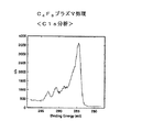
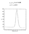
XPS(原子比F/C、CF2/CおよびCF3/C)
フッ素プラズマ処理後のサンプル基板の表面状態をXPS(アルバック・ファイ社QUANTUM2000)により分析した。分析はフッ素原子F1s(結合エネルギー:680〜700eV)と炭素原子C1s(結合エネルギー:280〜300eV)について行い、それぞれのピーク強度の比を算出し、当該比を最表面におけるフッ素原子数と炭素原子数の比(F/C)とした。またC1sピークは通常285eVに現れるが、フッ素原子が結合すると高エネルギー側にシフトする。カーボン原子にフッ素原子が2つ結合したCF2結合は292eVに、フッ素原子が3つ結合したCF3結合は294eVにそれぞれ現れる。それぞれのピーク強度の比(CF2/CおよびCF3/C)を算出し、それぞれの結合量の比とした。
XPS (atomic ratio F / C, CF 2 / C and CF 3 / C)
The surface state of the sample substrate after the fluorine plasma treatment was analyzed by XPS (ULVAC-PHI QUANTUM 2000). The analysis is performed for fluorine atoms F1s (bonding energy: 680 to 700 eV) and carbon atoms C1s (bonding energy: 280 to 300 eV), the ratio of the respective peak intensities is calculated, and the ratio is calculated based on the number of fluorine atoms and carbon atoms on the outermost surface. The ratio of numbers (F / C). The C1s peak usually appears at 285 eV, but shifts to the high energy side when fluorine atoms are bonded. A CF 2 bond in which two fluorine atoms are bonded to a carbon atom appears at 292 eV, and a CF 3 bond in which three fluorine atoms are bonded appears at 294 eV. The ratio of the respective peak intensities (CF 2 / C and CF 3 / C) was calculated and used as the ratio of the respective binding amounts.
<実験例1>
アルミニウム製の基板(10cm×10cm)の表面を、イエプコ処理し、種々の二乗平均傾斜Δqを有する粗面を有するプラズマ未処理サンプル基板を作製した。このように粗面化されたプラズマ未処理サンプル基板に次の条件で炭素イオンを注入し、さらにDLC層(厚み0.1μm)及び含フッ素原子層(厚み5nm)を形成し、フッ素プラズマ処理されたサンプル基板を作製した。(尚、プラズマ未処理サンプル基板の二乗平均傾斜Δqと、フッ素プラズマ処理基板の含フッ素原子層の二乗平均傾斜Δqとは同一であった。)
<Experimental example 1>
The surface of the aluminum substrate (10 cm × 10 cm) was subjected to Epco treatment to produce a plasma untreated sample substrate having rough surfaces having various root mean square slopes Δq. Carbon ions are implanted into the plasma-untreated sample substrate thus roughened under the following conditions, and further a DLC layer (thickness 0.1 μm) and a fluorine-containing atomic layer (thickness 5 nm) are formed and subjected to fluorine plasma treatment. A sample substrate was prepared. (The mean square slope Δq of the plasma untreated sample substrate and the mean square slope Δq of the fluorine-containing atomic layer of the fluorine plasma treated substrate were the same.)
炭素イオンの注入・DLC層の形成・含フッ素原子層の形成については、プラズマイオン注入法の原理を利用した。それぞれ使用する原料ガスを適当な圧力でチャンバー内に導入し、適当な高周波電力を負荷してプラズマ状態を生成し、サンプル基板に適当なバイアス電圧を印加して各処理を行った。使用した原料ガスと基板バイアス電圧を表1に示した。 For the implantation of carbon ions, the formation of the DLC layer, and the formation of the fluorine-containing atomic layer, the principle of the plasma ion implantation method was used. Each source gas used was introduced into the chamber at an appropriate pressure, an appropriate high frequency power was applied to generate a plasma state, and an appropriate bias voltage was applied to the sample substrate to perform each treatment. The source gas used and the substrate bias voltage are shown in Table 1.

また、比較のために、研磨加工により、上記アルミニウム基板の表面を粗面化し、種々の平均表面粗さRaを有する中心線粗さ基準を作製し、この上に、上記と全く同様にして、炭素イオンの注入、DLC層の形成及び含フッ素原子層の形成を行い、上記の平均表面粗さRaを有する中心線粗さ基準のフッ素プラズマ処理基板を作製した。 In addition, for comparison, the surface of the aluminum substrate is roughened by polishing, and a centerline roughness standard having various average surface roughness Ra is produced. Carbon ion implantation, DLC layer formation, and fluorine-containing atomic layer formation were performed to produce a centerline roughness-based fluorine plasma-treated substrate having the above average surface roughness Ra.
先ず、フッ素プラズマ処理基板のそれぞれについて、オリゴマー付着量を測定し、その二乗平均傾斜Δqとオリゴマー付着量とを図2にプロットした。図2の結果から、二乗平均傾斜Δqとオリゴマー付着量との間には相関関係があることが判る。 First, the oligomer adhesion amount was measured for each of the fluorine plasma-treated substrates, and the root mean square Δq and the oligomer adhesion amount were plotted in FIG. From the results of FIG. 2, it can be seen that there is a correlation between the mean square slope Δq and the amount of oligomer adhesion.
また、中心線粗さ基準のフッ素プラズマ処理基板のそれぞれについて、オリゴマー付着量を測定し、その平均表面粗さRaとオリゴマー付着量とを図3にプロットした。図3の結果から、平均表面粗さRaとオリゴマー付着量との間には相関関係が全くないことが判る。 Further, the oligomer adhesion amount was measured for each of the fluorine plasma treated substrates based on the center line roughness, and the average surface roughness Ra and the oligomer adhesion amount were plotted in FIG. From the results in FIG. 3, it can be seen that there is no correlation between the average surface roughness Ra and the amount of oligomer attached.
プラズマ未処理サンプル基板のそれぞれと、プラズマ処理基板のそれぞれについて、水に対する接触角を測定し、接触角と二乗平均傾斜Δqとを図4にプロットした。図4の結果から、プラズマ処理基板では、二乗平均傾斜Δqが6度より大きくなるにしたがい、接触角が増大し、表面エネルギーが低減していくことが判る。一方、プラズマ未処理サンプル基板では、二乗平均傾斜Δqが約5度を越えるにしたがい、接触角が小さくなっていく。 For each of the plasma untreated sample substrates and each of the plasma treated substrates, the contact angle with respect to water was measured, and the contact angle and the root mean square Δq were plotted in FIG. From the results of FIG. 4, it can be seen that in the plasma-treated substrate, the contact angle increases and the surface energy decreases as the root mean square Δq becomes larger than 6 degrees. On the other hand, in the plasma untreated sample substrate, the contact angle decreases as the mean square inclination Δq exceeds about 5 degrees.
プラズマ未処理サンプル基板のそれぞれと、プラズマ処理基板のそれぞれについて、オリゴマー付着量を測定し、その二乗平均傾斜Δqとオリゴマー付着量とを図5にプロットした。図5の結果から、フッ素プラズマ処理により形成された含フッ素原子層の二乗平均傾斜Δqが6度を越え、さらに7度以上となると、オリゴマー付着量が未処理のものに比して低減され、耐汚染性が向上することが判る。 The oligomer adhesion amount was measured for each of the plasma untreated sample substrates and each of the plasma treatment substrates, and the root mean square Δq and the oligomer adhesion amount were plotted in FIG. From the results of FIG. 5, when the root mean square slope Δq of the fluorine-containing atomic layer formed by the fluorine plasma treatment exceeds 6 degrees, and further becomes 7 degrees or more, the amount of oligomer adhesion is reduced as compared with the untreated one, It can be seen that the contamination resistance is improved.
<実験例2>
実験例1で作製された二乗平均傾斜Δqが7度のプラズマ処理基板について、XPSにより、表面の含フッ素原子層についてC1s及びF1s分析を行い、そのチャートを、図6及び図7に示した。図6から、CF2結合及びCF3結合が生成していることが判る。
<Experimental example 2>
C1s and F1s analyzes were performed on the fluorine-containing atomic layer on the surface of the plasma-treated substrate produced in Experimental Example 1 having a root mean square Δq of 7 degrees by XPS, and the charts are shown in FIGS. 6 and 7. From FIG. 6, it can be seen that CF 2 bonds and CF 3 bonds are generated.
また、F1sピークとC1sピークとの比から及び原子比(F/C)を算出したところ、F/C=3.0であった。このフッ素プラズマ処理基板でのオリゴマー付着量は、図1及び図5から約0.1mgである。 Moreover, it was F / C = 3.0 when the atomic ratio (F / C) was computed from the ratio of F1s peak and C1s peak. The oligomer adhesion amount on this fluorine plasma processing substrate is about 0.1 mg from FIG. 1 and FIG.
また、上記のプラズマ未処理基板の作製に用いたプラズマ未処理基板を使用し、反応ガスをC4F8からCF4に変更してのフッ素プラズマ処理を行った以外は、実験例1と全く同様にしてフッ素プラズマ処理基板を作製した。このプラズマ処理基板について、XPSにより、表面の含フッ素原子層についてC1s及びF1s分析を行い、そのチャートを、図8及び図9に示した。図8から、この基板では、CF2結合及びCF3結合が生成していないことが判る。 Moreover, it is completely the same as Experimental Example 1 except that the plasma untreated substrate used for the production of the plasma untreated substrate was used and the fluorine plasma treatment was performed by changing the reaction gas from C 4 F 8 to CF 4. Similarly, a fluorine plasma-treated substrate was produced. This plasma-treated substrate was subjected to C1s and F1s analysis on the surface fluorine-containing atomic layer by XPS, and the charts thereof are shown in FIGS. From FIG. 8, it can be seen that CF 2 bonds and CF 3 bonds are not generated in this substrate.
また、F1sピークとC1sピークとの比から及び原子比(F/C)を算出したところ、F/C=0.8であった。このフッ素プラズマ処理基板について、オリゴマー付着量を測定したところ、0.3mgであった。 Moreover, it was F / C = 0.8 when the atomic ratio (F / C) was computed from the ratio of F1s peak and C1s peak. With respect to this fluorine plasma-treated substrate, the amount of adhered oligomer was measured and found to be 0.3 mg.
以上の結果から、原子比(F/C)が1.0以上であり、CF2結合やCF3結合が生成している含フッ素原子層が形成されている場合には、原子比(F/c)が1.0未満であり、CF2結合やCF3結合が生成していない場合に比して、オリゴマー付着量が低減され、耐汚染性が向上していることが判る。 From the above results, when the atomic ratio (F / C) is 1.0 or more and a fluorine-containing atomic layer in which CF 2 bonds or CF 3 bonds are formed is formed, the atomic ratio (F / C) It can be seen that c) is less than 1.0, and the amount of oligomer adhesion is reduced and the contamination resistance is improved as compared with the case where no CF 2 bond or CF 3 bond is formed.
1:金属製基板
3:ダイヤモンド状カーボン(DLC)層
5:含フッ素原子層
1: Metal substrate 3: Diamond-like carbon (DLC) layer 5: Fluorine-containing atomic layer
Claims (6)
Priority Applications (1)
| Application Number | Priority Date | Filing Date | Title |
|---|---|---|---|
| JP2006178643A JP4702201B2 (en) | 2006-06-28 | 2006-06-28 | Resin processing parts |
Applications Claiming Priority (1)
| Application Number | Priority Date | Filing Date | Title |
|---|---|---|---|
| JP2006178643A JP4702201B2 (en) | 2006-06-28 | 2006-06-28 | Resin processing parts |
Publications (2)
| Publication Number | Publication Date |
|---|---|
| JP2008006659A JP2008006659A (en) | 2008-01-17 |
| JP4702201B2 true JP4702201B2 (en) | 2011-06-15 |
Family
ID=39065306
Family Applications (1)
| Application Number | Title | Priority Date | Filing Date |
|---|---|---|---|
| JP2006178643A Active JP4702201B2 (en) | 2006-06-28 | 2006-06-28 | Resin processing parts |
Country Status (1)
| Country | Link |
|---|---|
| JP (1) | JP4702201B2 (en) |
Families Citing this family (3)
| Publication number | Priority date | Publication date | Assignee | Title |
|---|---|---|---|---|
| JP5211819B2 (en) * | 2008-04-14 | 2013-06-12 | トヨタ紡織株式会社 | Method for producing vegetable fiber molded body |
| JP4858507B2 (en) * | 2008-07-31 | 2012-01-18 | トーカロ株式会社 | Carrier for holding an object to be polished |
| JP6044144B2 (en) * | 2012-07-11 | 2016-12-14 | 凸版印刷株式会社 | Manufacturing method of preform injection mold |
Citations (6)
| Publication number | Priority date | Publication date | Assignee | Title |
|---|---|---|---|---|
| JPH01138611A (en) * | 1987-11-26 | 1989-05-31 | Nec Corp | Magnetic disk |
| JPH09194227A (en) * | 1995-08-29 | 1997-07-29 | Yasuaki Sakamoto | Mold for press forming and glass master disk formed thereby |
| JPH09300428A (en) * | 1996-05-20 | 1997-11-25 | Toray Ind Inc | Cap |
| JP2004144582A (en) * | 2002-10-23 | 2004-05-20 | Fuji Seisakusho:Kk | Hardness determination method and hardness determination system |
| JP2006032423A (en) * | 2004-07-12 | 2006-02-02 | Toshiba Corp | Stamper for imprint processing and manufacturing method thereof |
| JP2007266384A (en) * | 2006-03-29 | 2007-10-11 | Toppan Printing Co Ltd | Mold for imprinting and manufacturing method thereof |
Family Cites Families (1)
| Publication number | Priority date | Publication date | Assignee | Title |
|---|---|---|---|---|
| JP5075411B2 (en) * | 2004-09-30 | 2012-11-21 | 東洋製罐株式会社 | Fluororesin-coated mold for molding polyester containers and method for recycling the same |
-
2006
- 2006-06-28 JP JP2006178643A patent/JP4702201B2/en active Active
Patent Citations (6)
| Publication number | Priority date | Publication date | Assignee | Title |
|---|---|---|---|---|
| JPH01138611A (en) * | 1987-11-26 | 1989-05-31 | Nec Corp | Magnetic disk |
| JPH09194227A (en) * | 1995-08-29 | 1997-07-29 | Yasuaki Sakamoto | Mold for press forming and glass master disk formed thereby |
| JPH09300428A (en) * | 1996-05-20 | 1997-11-25 | Toray Ind Inc | Cap |
| JP2004144582A (en) * | 2002-10-23 | 2004-05-20 | Fuji Seisakusho:Kk | Hardness determination method and hardness determination system |
| JP2006032423A (en) * | 2004-07-12 | 2006-02-02 | Toshiba Corp | Stamper for imprint processing and manufacturing method thereof |
| JP2007266384A (en) * | 2006-03-29 | 2007-10-11 | Toppan Printing Co Ltd | Mold for imprinting and manufacturing method thereof |
Also Published As
| Publication number | Publication date |
|---|---|
| JP2008006659A (en) | 2008-01-17 |
Similar Documents
| Publication | Publication Date | Title |
|---|---|---|
| Tyagi et al. | A critical review of diamond like carbon coating for wear resistance applications | |
| JP5075411B2 (en) | Fluororesin-coated mold for molding polyester containers and method for recycling the same | |
| US20020014325A1 (en) | Metal substrate with a corrosion-resistant coating produced by means of plasma polymerisation | |
| EP0363103A2 (en) | Method of conducting electrostatic coating of crystalline thermoplastic resin molding and coated plastic molding | |
| WO2001011612A1 (en) | Tray for conveying magnetic head for magnetic disk | |
| JP4702201B2 (en) | Resin processing parts | |
| JP5149069B2 (en) | Mold assembly and injection molding method | |
| KR101455142B1 (en) | Process for production of coated article having excellent corrosion resistance, and coated article | |
| JP4844788B2 (en) | Fluorine-containing copolymer | |
| TWI711720B (en) | Surface material of metal mold forming surface and surface treatment method of metal mold forming surface | |
| TWI568870B (en) | Tubular target comprising a protective device | |
| CN1604823A (en) | Articles spray coated with non-melting polymer | |
| Šadl et al. | Protective alumina coatings prepared by aerosol deposition on magnetocaloric gadolinium elements | |
| JP2005190632A (en) | Optical disk molding die on which diamond like carbon is film-deposited and optical disk molding method using the same | |
| JP4458911B2 (en) | Plastics composite material and manufacturing method thereof | |
| JP6546143B2 (en) | Method of manufacturing injection molded articles | |
| JP2010260216A (en) | Fluororesin molding and method for manufacturing the same | |
| KR100977378B1 (en) | Method for coating the inside of an extruder die and a die coated thereby | |
| EP3724376B1 (en) | Electroplating tool | |
| JP4617678B2 (en) | Melt spinneret, method for producing the same, and melt spinning method using the same | |
| JP4442201B2 (en) | Method for producing fluororesin coated member | |
| KR102317383B1 (en) | Covering member and manufacturing method thereof | |
| JP2002018858A (en) | Mold for polyester container | |
| JP4494913B2 (en) | Optical element manufacturing method | |
| JP2017209876A (en) | Molding die |
Legal Events
| Date | Code | Title | Description |
|---|---|---|---|
| A621 | Written request for application examination |
Free format text: JAPANESE INTERMEDIATE CODE: A621 Effective date: 20090512 |
|
| TRDD | Decision of grant or rejection written | ||
| A01 | Written decision to grant a patent or to grant a registration (utility model) |
Free format text: JAPANESE INTERMEDIATE CODE: A01 Effective date: 20110208 |
|
| A61 | First payment of annual fees (during grant procedure) |
Free format text: JAPANESE INTERMEDIATE CODE: A61 Effective date: 20110221 |
|
| R150 | Certificate of patent or registration of utility model |
Ref document number: 4702201 Country of ref document: JP Free format text: JAPANESE INTERMEDIATE CODE: R150 |
|
| FPAY | Renewal fee payment (event date is renewal date of database) |
Free format text: PAYMENT UNTIL: 20140318 Year of fee payment: 3 |
|
| S531 | Written request for registration of change of domicile |
Free format text: JAPANESE INTERMEDIATE CODE: R313531 |
|
| FPAY | Renewal fee payment (event date is renewal date of database) |
Free format text: PAYMENT UNTIL: 20140318 Year of fee payment: 3 |
|
| R350 | Written notification of registration of transfer |
Free format text: JAPANESE INTERMEDIATE CODE: R350 |
|
| S533 | Written request for registration of change of name |
Free format text: JAPANESE INTERMEDIATE CODE: R313533 |
|
| FPAY | Renewal fee payment (event date is renewal date of database) |
Free format text: PAYMENT UNTIL: 20140318 Year of fee payment: 3 |
|
| R350 | Written notification of registration of transfer |
Free format text: JAPANESE INTERMEDIATE CODE: R350 |
|
| S111 | Request for change of ownership or part of ownership |
Free format text: JAPANESE INTERMEDIATE CODE: R313111 |
|
| R350 | Written notification of registration of transfer |
Free format text: JAPANESE INTERMEDIATE CODE: R350 |