JP4688703B2 - USB transceiver - Google Patents
USB transceiver Download PDFInfo
- Publication number
- JP4688703B2 JP4688703B2 JP2006066841A JP2006066841A JP4688703B2 JP 4688703 B2 JP4688703 B2 JP 4688703B2 JP 2006066841 A JP2006066841 A JP 2006066841A JP 2006066841 A JP2006066841 A JP 2006066841A JP 4688703 B2 JP4688703 B2 JP 4688703B2
- Authority
- JP
- Japan
- Prior art keywords
- circuit
- signal
- output signal
- output
- input
- Prior art date
- Legal status (The legal status is an assumption and is not a legal conclusion. Google has not performed a legal analysis and makes no representation as to the accuracy of the status listed.)
- Expired - Fee Related
Links
Images


Landscapes
- Dc Digital Transmission (AREA)
- Logic Circuits (AREA)
Description
本発明は、ユニバーサル・シリアル・バス(Universal Serial Bus:以下、USBと略記)対応機器間で複数のデータ信号を転送するために、それらの機器に搭載されUSBを通じて複数のデータ信号を送受信するUSBトランシーバに関するものである。 In order to transfer a plurality of data signals between universal serial bus (Universal Serial Bus: abbreviated as USB) compatible devices, the present invention is mounted on these devices and transmits and receives a plurality of data signals through the USB. It relates to transceivers.
近年、携帯電話、PDA端末やノートパソコンなどの携帯電子機器や、その周辺機器の接続には、USBがよく利用されるようになってきている。
このようなUSBは、2本の信号線を用いてシリアルデータを伝送する方式であり、特に、シリアルデータの受信回路においては、2本の信号線が、差動コンパレータ回路とシングルエンデッドレシーバ回路に接続される。差動コンパレータ回路は、2本の信号線の差分信号を出力し、シングルエンデッドレシーバ回路は、各信号線を波形整形し、コントローラ側に出力する。
In recent years, USB is often used for connection of portable electronic devices such as mobile phones, PDA terminals and notebook personal computers, and peripheral devices.
Such USB is a method of transmitting serial data using two signal lines. In particular, in a serial data receiving circuit, two signal lines include a differential comparator circuit and a single-ended receiver circuit. Connected to. The differential comparator circuit outputs a differential signal between the two signal lines, and the single-ended receiver circuit shapes the waveform of each signal line and outputs it to the controller side.
以上のような従来のUSBトランシーバ(例えば、特許文献1を参照)について、図面を用いて以下に説明する。このUSBトランシーバは、リーク電流対策に関するものであり図3に示すような回路構成で示される。 A conventional USB transceiver as described above (see, for example, Patent Document 1) will be described below with reference to the drawings. This USB transceiver relates to leakage current countermeasures and is shown in a circuit configuration as shown in FIG.
図3は従来のUSBトランシーバの構成を示す回路ブロック図である。図3において、33a、33bはUSBデータの受信入力端子、35は受信入力端子33a、33bからのUSBデータが入力信号となる差動コンパレータ回路、36は受信入力端子33aからのUSBデータを入力信号に持つシングルエンデッドレシーバ回路、37は受信入力端子33bからのUSBデータを入力信号に持つシングルエンデッドレシーバ回路、40は差動コンパレータ回路35の出力端子、38はシングルエンデッドレシーバ回路36の出力端子、39はシングルエンデッドレシーバ回路37の出力端子であり、ドライバ回路41は、コントローラ側からの制御端子である入力端子42、43のドライブ信号をバッファし、その出力信号により、USBデータの受信入力端子33a、33bを共通使用する出力端子を駆動するような回路構成になっている。
FIG. 3 is a circuit block diagram showing the configuration of a conventional USB transceiver. In FIG. 3, 33a and 33b are USB data reception input terminals, 35 is a differential comparator circuit in which USB data from the
ここで、ドライバ回路41は、その出力信号が双方向・半二重動作をサポートする構成になっている。また、差動コンパレータ回路35はMOS差動アンプ等により構成され、複数のトランジスタが必要であり、シングルエンデッドレシーバ回路36、37は論理バッファによる比較的少数のトランジスタで回路が構成される。さらに、出力端子38、39、40はコントローラ側にデータを出力する。
しかしながら、上記のような従来のUSBトランシーバでは、その構成要素である差動コンパレータ回路35とシングルエンデッドレシーバ回路36、37との間で、それらの回路構成規模が異なるため、USBデータの受信入力端子33a、33bからの入力信号に対して、各回路間の伝達遅延時間差により、各回路の出力端子38、39、40から出力される信号のスキューが大きくなってしまう。
However, in the conventional USB transceiver as described above, the
一方、それらの出力端子38、39、40からの出力信号を入力信号とするコントローラ側のマイコンは、例えばフルスピード(12Mbps)のUSBデータを通信する場合は、通常12Mbpsの4倍以上のサンプリングによりデータ処理を行うが、12Mbps(パルス幅83.3ns)の4倍サンプリング時のパルス幅は20.8nsであるため、例えば、差動コンパレータ回路35の出力端子40側とシングルエンデッドレシーバ回路36、37の出力端子38、39側とで、それらの各信号間の伝達遅延時間差が20.8ns以上になると、コントローラ側で、各信号の取り込みタイミングが互いにずれてしまう。
On the other hand, the microcomputer on the controller side using the output signals from these
すなわち、各信号の取り込みタイミングによっては、出力端子38、39、40の各信号間で互いに動作上のタイミングずれが発生することになり、これらの各信号を受信したコントローラ側のマイコンが動作エラーとなって、コントローラ側を含む当該システムの誤動作の原因になる場合がある。
That is, depending on the timing at which each signal is captured, there is an operational timing shift between the signals at the
以上のように、USBトランシーバを構成する各回路間の伝達遅延時間差によって出力信号のスキューが大きくなる様子を、図4を用いて以下に説明する。
図4は図3を用いて説明した従来のUSBトランシーバの各端子における電圧状態を示す波形図である。ここで、PACKET期間は受信入力端子33a、33bのそれぞれからUSBデータが互いに逆位相で入力される期間であり、EOP期間は受信入力端子33a、33bのそれぞれからUSBデータが互いに同一位相で入力される期間である。また、T1、T2、T3、T4は出力波形の時間軸上の各タイミングにおける遅延時間である。
The manner in which the skew of the output signal increases due to the transmission delay time difference between the circuits constituting the USB transceiver as described above will be described below with reference to FIG.
FIG. 4 is a waveform diagram showing a voltage state at each terminal of the conventional USB transceiver described with reference to FIG. Here, the PACKET period is a period in which the USB data is input from the
図4に示す入力波形401のUSBデータが受信入力端子33aに入力されると、シングルエンデッドレシーバ回路36の出力端子38には、受信入力端子33aの信号と同位相の波形404が出力され、同様に図4に示す入力波形402のUSBデータが受信入力端子33bに入力されると、シングルエンデッドレシーバ回路37の出力端子39には、受信入力端子33bの信号と同位相の波形405が出力される。
When the USB data of the
入力波形401、402のUSBデータが受信入力端子33a、33bへ互いに逆位相で入力される期間(PACKET)では、受信入力端子33a、33bからのUSBデータを入力とする差動コンパレータ回路35が動作し、出力端子40には、入力信号に対して回路伝達時間に差が生じ、ロウレベルからハイレベルに変化する時に遅延時間T1を持ち、ハイレベルからロウレベルに変化する時に遅延時間T3を持った波形403におけるPACKET期間のような信号が出力される。
During the period (PACKET) in which the USB data of the
次に、入力波形401、402のUSBデータが受信入力端子33a、33bへ互いに同一位相で入力される期間(EOP)では、受信入力端子33a、33bからのUSBデータを入力とする差動コンパレータ回路35は動作せず、通常は入力信号ノイズの影響を受けないようにするため、その出力側を所定の電位レベル(図4においてはロウレベル)に固定されている。したがって、出力端子40には波形403におけるEOP期間のような信号が出力される。
Next, in a period (EOP) in which the USB data of the
なお、シングルエンデッドレシーバ回路36とシングルエンデッドレシーバ回路37との信号伝達時間差は、各シングルエンデッドレシーバ回路36、37と差動コンパレータ回路35との信号伝達時間差に対し、ほとんど無視できる時間差であり、図4において特に図示していない。
The signal transmission time difference between the single-
本発明は、上記従来の問題点を解決するもので、USBを通じて受信した入力データ信号に対して、差動コンパレータ回路とシングルエンデッドレシーバ回路の伝達遅延の時間差を精度よく補正することができるUSBトランシーバを提供する。 The present invention solves the above-mentioned conventional problems, and a USB capable of accurately correcting a time difference in transmission delay between a differential comparator circuit and a single-ended receiver circuit with respect to an input data signal received through the USB. Provide a transceiver.
上記の課題を解決するために、本発明の請求項1記載のUSBトランシーバは、第1の信号線と第2の信号線のシリアルデータを送受信するUSBトランシーバであって、前記第1の信号線と前記第2の信号線にデータ信号をドライブするドライバ回路と、前記第1の信号線と前記第2の信号線のデータ信号を差動入力する差動コンパレータ回路と、前記第1の信号線のデータ信号を入力する第1のシングルエンデッドレシーバ回路と、前記第2の信号線のデータ信号を入力する第2のシングルエンデッドレシーバ回路と、前記第1のシングルエンデッドレシーバ回路の出力信号を遅延させる第1の遅延回路部と、前記第2のシングルエンデッドレシーバ回路の出力信号を遅延させる第2の遅延回路部と、前記差動コンパレータ回路の出力信号と前記第1の遅延回路部の出力信号と前記第2の遅延回路部の出力信号とが入力される論理回路部とを具備し、前記論理回路部は、前記第1の信号線と前記第2の信号線のデータ信号が互いに逆位相でレベル変化した場合において、前記第1の遅延回路部の出力信号を、前記差動コンパレータ回路の出力信号に基いて、前記第1のシングルエンデッドレシーバ回路の出力信号のレベル変化を前記差動コンパレータ回路の出力信号のレベル変化に同期させた信号に変換して、前記第2の遅延回路部の出力信号を、前記差動コンパレータ回路の出力信号に基いて、前記第2のシングルエンデッドレシーバ回路の出力信号のレベル変化を前記差動コンパレータ回路の出力信号のレベル変化に同期させた信号に変換するよう構成したことを特徴とする。 In order to solve the above problems, a USB transceiver according to claim 1 of the present invention is a USB transceiver for transmitting and receiving serial data of a first signal line and a second signal line, wherein the first signal line And a driver circuit for driving a data signal to the second signal line, a differential comparator circuit for differentially inputting the data signal of the first signal line and the second signal line, and the first signal line A first single-ended receiver circuit that inputs a data signal of the second signal, a second single-ended receiver circuit that inputs a data signal of the second signal line, and an output signal of the first single-ended receiver circuit A first delay circuit section for delaying the output signal, a second delay circuit section for delaying an output signal of the second single-ended receiver circuit, and an output signal of the differential comparator circuit And a logic circuit unit to which an output signal of the first delay circuit unit and an output signal of the second delay circuit unit are input, and the logic circuit unit includes the first signal line and the first signal line. in no event the data signal and second signal line has a level change in phases opposite to each other, the output signal of said first delay circuit, based on an output signal of the differential comparator circuit, the first single-ended The level change of the output signal of the dead receiver circuit is converted into a signal synchronized with the level change of the output signal of the differential comparator circuit, and the output signal of the second delay circuit unit is output from the differential comparator circuit. based on the signal, to characterized in that it is configured to convert a change in level of the output signal of said second single-ended receiver circuit into a signal synchronized with the level change of the output signal of the differential comparator circuit .
また、本発明の請求項2記載のUSBトランシーバは、請求項1記載のUSBトランシーバであって、前記第1の遅延回路部は、前記第1のシングルエンデッドレシーバ回路の出力信号の立ち上がり時のみ遅延させる第1の立ち上がり遅延回路と、立ち下がり時のみ遅延させる第1の立ち下がり遅延回路とを具備し、前記第2の遅延回路部は、前記第2のシングルエンデッドレシーバ回路の出力信号の立ち上がり時のみ遅延させる第2の立ち上がり遅延回路と、立ち下がり時のみ遅延させる第2の立ち下がり遅延回路とを具備し、前記論理回路部は、前記第1の立ち下がり遅延回路の出力信号と前記差動コンパレータ回路の出力信号とが入力される第1のAND回路と、前記第1の立ち上がり遅延回路の出力信号と前記第1のAND回路の出力信号とが入力されるOR回路と、前記第2の立ち下がり遅延回路の出力信号と前記差動コンパレータ回路の出力信号とが入力される第2のAND回路と、前記第2の立ち上がり遅延回路の出力信号と前記第2のAND回路の出力信号とが入力されるNOR回路とを具備したことを特徴とする。 The USB transceiver according to claim 2 of the present invention is the USB transceiver according to claim 1, wherein the first delay circuit unit is only at the rising edge of the output signal of the first single-ended receiver circuit. A first rising delay circuit for delaying, and a first falling delay circuit for delaying only at the time of falling, and the second delay circuit section outputs an output signal of the second single-ended receiver circuit. A second rising delay circuit that delays only at the time of rising; and a second falling delay circuit that delays only at the time of falling, and the logic circuit section outputs the output signal of the first falling delay circuit and the A first AND circuit to which an output signal of the differential comparator circuit is input; an output signal of the first rising delay circuit; and an output of the first AND circuit. An OR circuit to which a signal is input, a second AND circuit to which an output signal of the second falling delay circuit and an output signal of the differential comparator circuit are input, and a second rising delay circuit And a NOR circuit to which the output signal and the output signal of the second AND circuit are input .
以上のように本発明によれば、USBを通じて受信した入力データ信号に対して、差動コンパレータ回路とシングルエンデッドレシーバ回路の伝達遅延の時間差を精度よく補正することにより、USBを通じて受信した差動形式の複数のデータ信号をコントローラ側に送る際に、それら複数のデータ信号のレベル変化が同期するように、それらの信号間に生じるレベル変化のタイミングずれ(スキュー)を常にかつ確実に最小状態に維持することができる。 As described above, according to the present invention, the differential data received through the USB is corrected by accurately correcting the time difference of the transmission delay between the differential comparator circuit and the single-ended receiver circuit with respect to the input data signal received through the USB. When sending multiple data signals in the format to the controller side, the timing shift (skew) of the level changes that occur between these signals is always minimized to ensure that the level changes of the multiple data signals are synchronized. Can be maintained.
また、USBの差動形式で受信した入力データ信号のどちらかが、外的要因などで入力データ信号にレベル変化のタイミングずれが生じた場合でも、複数のデータ信号間に生じるレベル変化のタイミングずれを常にかつ確実に最小状態に維持することができる。 In addition, even if one of the input data signals received in the USB differential format has a level change timing shift in the input data signal due to an external factor or the like, the level change timing shift that occurs between the multiple data signals Can always be maintained in a minimum state.
以上により、USBを通じてコントローラ側へ入力されたデータ信号に対して、コントローラ側のマイコンへの取り込みのタイミングずれをなくして、コントローラ側でのデータ信号の取り込みエラーの発生を抑えることができ、システム全体での誤動作を確実になくすことができる。 As described above, the data signal input to the controller side via USB can be eliminated, and the occurrence of errors in the data signal acquisition on the controller side can be suppressed by eliminating the timing difference in the data acquisition to the controller side microcomputer. It is possible to reliably eliminate malfunctions.
以下、本発明の実施の形態を示すUSBトランシーバについて、図面を参照しながら具体的に説明する。
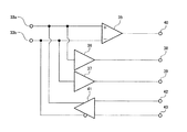
図1は本実施の形態のUSBトランシーバの構成を示す回路ブロック図である。図1において、3a、3bはUSBデータの受信入力端子、5は差動コンパレータ回路、6はシングルエンデッドレシーバ回路、7はシングルエンデッドレシーバインバータ回路、8はシングルエンデッドレシーバ回路6の出力信号、9はシングルエンデッドレシーバインバータ回路7の出力信号、10、13は立ち上がり遅延回路、11、12は立ち下がり遅延回路、14はOR回路、15、16はAND回路、17はNOR回路、18、19、20は出力端子、21はドライバ回路、22、23はコントローラ側から制御される入力端子である。ここで、立ち上がり遅延回路10、13と立ち下がり遅延回路11、12で遅延回路部を構成し、OR回路14とAND回路15、16とNOR回路17で論理回路部を構成する。
Hereinafter, a USB transceiver showing an embodiment of the present invention will be specifically described with reference to the drawings.
FIG. 1 is a circuit block diagram showing the configuration of the USB transceiver of this embodiment. In FIG. 1, 3a and 3b are USB data reception input terminals, 5 is a differential comparator circuit, 6 is a single-ended receiver circuit, 7 is a single-ended receiver inverter circuit, and 8 is an output signal of the single-
装置構成としては、シングルエンデッドレシーバ回路6の入力にUSBデータの受信入力端子3aが、シングルエンデッドレシーバインバータ回路7の入力にUSBデータの受信入力端子3bが、そしてUSBデータの受信入力端子3a、3bにそれらのUSBデータを入力信号とする差動コンパレータ回路5が、それぞれ接続されている。
The device configuration includes a USB data
シングルエンデッドレシーバ回路6の出力は、立ち上がり遅延回路10と立ち下がり遅延回路11の入力に接続され、シングルエンデッドレシーバ回路6の出力電圧の変化するエッジを検出し、立ち下がり遅延回路11の出力と差動コンパレータ回路5の出力は、AND回路15の入力に接続され、AND回路15の出力と立ち上がり遅延回路10の出力はOR回路14の入力に接続され、OR回路14の出力はUSBデータの受信入力端子3a側の出力端子18へ接続される。
The output of the single-
同様に、シングルエンデッドレシーバインバータ回路7の出力は、立ち上がり遅延回路13と立ち下がり遅延回路12の入力に接続され、シングルエンデッドレシーバインバータ回路7の出力電圧の変化するエッジを検出し、立ち下がり遅延回路12の出力と差動コンパレータ回路5の出力は、AND回路16の入力に接続され、AND回路16の出力と立ち上がり遅延回路13の出力はNOR回路17の入力に接続され、NOR回路17の出力はUSBデータの受信入力端子3b側の出力端子19へ接続される。
Similarly, the output of the single-ended
ドライバ回路21は、コントローラ側からの制御端子である入力端子22、23のドライブ信号をバッファし、その出力信号により、USBデータの受信入力端子3a、3bを共通使用する出力端子を駆動するような回路構成になっている。ここで、ドライバ回路21は、その出力信号が双方向・半二重動作をサポートする構成になっている。
The
以上のように構成されたUSBトランシーバについて、その動作を図2を用いて以下に説明する。
図2は本実施の形態のUSBトランシーバにおける動作中の電圧状態を示す波形図である。図2において、PACKET期間は受信入力端子3a、3bのそれぞれからUSBデータが互いに逆位相で入力される期間であり、EOP期間は受信入力端子3a、3bのそれぞれからUSBデータが互いに同一位相で入力される期間である。また、T1、T2、T3、T4は出力波形の時間軸上の各タイミングにおける遅延時間である。また、PACKET期間において、受信入力端子3a、3bには、それぞれスキューのない入力波形201、202の信号が入力されているものとする。
The operation of the USB transceiver configured as described above will be described below with reference to FIG.
FIG. 2 is a waveform diagram showing a voltage state during operation in the USB transceiver of this embodiment. In FIG. 2, the PACKET period is a period in which USB data is input from the
受信入力端子3aから入力された波形201の信号は、シングルエンデッドレシーバ回路6に入力されると同時に、差動コンパレータ回路5の(+)端子にも入力される。また、同様に受信入力端子3bから入力された波形202の信号は、シングルエンデッドレシーバインバータ回路7に入力されると同時に、差動コンパレータ回路5の(−)端子にも入力される。
The signal of the
差動コンパレータ回路5は、受信入力端子3a、3bから波形201、202で示される入力信号を受けて動作し、出力端子20には、波形201、202の入力信号に対して、回路伝達時間により時間差が生じ、ロウレベルからハイレベルに変化する時に遅延時間T1を持ち、ハイレベルからロウレベルに変化する時に遅延時間T3を持った波形203の信号が出力される。
The differential comparator circuit 5 operates by receiving the input signals indicated by the
シングルエンデッドレシーバ回路6からの出力信号8は、波形204で示され、立ち上がり遅延回路10と立ち下がり遅延回路11に入力され、出力信号8の電圧変化を検出し、立ち上がり遅延回路10の出力はロウレベルからハイレベルに変化する信号について遅延時間T2を持った波形206の信号が出力され、立ち下がり遅延回路11の出力はハイレベルからロウレベルに変化する信号について遅延時間T4を持った波形207の信号が出力される。
An
そして、AND回路15には立ち下がり遅延回路11の出力信号と出力端子20の信号が入力され、そのAND回路15の出力信号は、波形210のように、ロウレベルからハイレベルに変化する時に遅延時間T1を持ち、ハイレベルからロウレベルへ変化する時に遅延時間T3を持つ信号となる。
Then, the output signal of the falling
AND回路15の出力信号と立ち上がり遅延回路10の出力信号がOR回路14に入力されることにより、出力端子18には、受信入力端子3aからの波形201の信号に対し、波形212のように、ロウレベルからハイレベルに変化する時に遅延時間T1を持ち、ハイレベルからロウレベルに変化する時に遅延時間T3を持つ信号が出力される。
When the output signal of the AND
ここで、AND回路15の出力と立ち上がり遅延回路10の出力をOR回路14により論理和を取っているのは、差動コンパレータ回路5の出力端子20にノイズ等が発生し、その電位レベルが変動した場合でも出力端子18の信号が変動しない効果を持たせるためである。
Here, the logical sum of the output of the AND
また、同様に、受信入力端子3bから受信入力端子3aの波形201とは逆位相の波形202で示される信号を入力するシングルエンデッドレシーバインバータ回路7は、その入力信号に対して反転された波形205で示される出力信号9に変換される。
Similarly, the single-ended
この出力信号9は、立ち下がり遅延回路12と立ち上がり遅延回路13とに入力され、出力信号9の電圧変化を検出し、立ち下がり遅延回路12の出力は、波形208で示されるように、受信入力端子3bのハイレベルからロウレベルに変化する信号について、遅延時間T2を持った信号が出力され、立ち上がり遅延回路13の出力は、波形209で示されるように、受信入力端子3bのロウレベルからハイレベルに変化する信号について、遅延時間T4を持った信号が出力される。
The
そして、AND回路16には立ち下がり遅延回路12の出力信号と出力端子20の信号が入力され、そのAND回路16の出力信号は、波形211のように、ロウレベルからハイレベルに変化する時に遅延時間T1を持ち、ハイレベルからロウレベルへ変化する時に遅延時間T3を持つ信号となる。
Then, the output signal of the falling
AND回路16の出力信号と立ち上がり遅延回路13の出力信号がNOR回路17に入力されることにより、出力端子19には、受信入力端子3bの信号に対し、波形213のように、ハイレベルからロウレベルに変化する時に遅延時間T1を持ち、ロウレベルからハイレベルに変化する時に遅延時間T3を持つ信号が出力される。
When the output signal of the AND
ここで、AND回路16の出力と立ち上がり遅延回路13の出力をNOR回路17により論理和を取っているのは、差動コンパレータ回路5の出力端子20にノイズ等が発生し、その電位レベルが変動した場合でも、出力端子19が変動しない効果を持たせるためである。
Here, the logical sum of the output of the AND
次に、受信入力端子3a、3bの各USBデータとして入力波形201、202が同一位相で入力されるEOP期間の動作を説明する。
受信入力端子3aから入力された波形201の信号は、シングルエンデッドレシーバ回路6に入力されると同時に、差動コンパレータ回路5の(+)端子にも入力される。また、同様に受信入力端子3bから入力された波形202の信号は、シングルエンデッドレシーバインバータ回路7に入力されると同時に、差動コンパレータ回路5の(−)端子にも入力される。
Next, the operation in the EOP period in which the
The signal of the
差動コンパレータ回路5は、EOP期間では、受信入力端子3a、3bに同一位相のUSBデータが入力されるため動作せず、出力端子20には、波形203のEOP期間の信号が出力される。出力端子18、19には、EOPの期間に受信入力端子3a、3bに入力されるUSBデータが変化した場合も、前述のPACKET期間と同様の回路動作により、同様の信号が出力される。
The differential comparator circuit 5 does not operate in the EOP period because USB data having the same phase is input to the
また、受信入力端子3a、3bから出力端子18、19への回路要因による伝達遅延時間の差が、出力端子18と出力端子19の間に発生しないように、各遅延回路10、11、12、13は、それぞれ同様の回路規模の構成にすることが望ましい。
The
なお、立ち上がり遅延回路10、13と立ち下がり遅延回路11、12の各回路の遅延時間T2、T4と、差動コンパレータ回路5の回路伝達遅延で生じる遅延時間T1、T3の関係は、それぞれT1<T2、T3<T4である必要がある。
The relationship between the delay times T2 and T4 of the rising
以上のように本実施の形態によれば、受信信号としてUSBデータの受信入力端子3a、3bに入力されたデータ信号は、回路伝達遅延の発生を最小限に抑えてスキューを最小状態に抑えたデータ信号にして、コントローラ側に接続される出力端子18、19、20からのデータ信号として、コントローラ側に出力することができる。
As described above, according to the present embodiment, the data signal input to the USB data
その結果、USBを通じてコントローラ側へ入力されたデータ信号に対して、コントローラ側のマイコンへの取り込みのタイミングずれをなくして、コントローラ側でのデータ信号の取り込みエラーの発生を抑えることができ、システム全体での誤動作を確実になくすことができる。 As a result, the data signal input to the controller side via USB can be eliminated, and the occurrence of errors in the data signal acquisition on the controller side can be suppressed by eliminating the timing deviation of the data acquisition to the controller side microcomputer. It is possible to reliably eliminate malfunctions.
本発明のUSBトランシーバは、USBを通じてコントローラ側へ入力されたデータ信号に対して、コントローラ側のマイコンへの取り込みのタイミングずれをなくして、コントローラ側でのデータ信号の取り込みエラーの発生を抑えることができ、システム全体での誤動作を確実になくすことができるもので、USB端子を搭載した携帯電話やPDA端末、パソコンなどの携帯電子機器や、その周辺機器等のUSB対応機器に有用である。 The USB transceiver according to the present invention eliminates a deviation in the timing of fetching data into the microcomputer on the controller side with respect to the data signal input to the controller side via the USB, and suppresses the occurrence of a data signal fetch error on the controller side. It is possible to reliably eliminate malfunctions in the entire system, and is useful for portable electronic devices such as mobile phones, PDA terminals and personal computers equipped with USB terminals, and USB compatible devices such as peripheral devices.
3a、3b、33a、33b USBデータの受信入力端子
5、35 差動コンパレータ回路
6、36、37 シングルエンデッドレシーバ回路
7 シングルエンデッドレシーバインバータ回路
8 シングルエンデッドレシーバ回路の出力信号
9 シングルエンデッドレシーバインバータ回路の出力信号
10、13 立ち上がり遅延回路
11、12 立ち下がり遅延回路
14 OR回路
15、16 AND回路
17 NOR回路
18、19、20、38、39、40 出力端子
21、41 ドライバ回路
22、23、42、43 入力端子
PACKET 逆位相入力期間
EOP 同一位相入力期間
T1、T2、T3、T4 遅延時間
3a, 3b, 33a, 33b USB data
Claims (2)
前記第1の信号線と前記第2の信号線にデータ信号をドライブするドライバ回路と、
前記第1の信号線と前記第2の信号線のデータ信号を差動入力する差動コンパレータ回路と、
前記第1の信号線のデータ信号を入力する第1のシングルエンデッドレシーバ回路と、
前記第2の信号線のデータ信号を入力する第2のシングルエンデッドレシーバ回路と、
前記第1のシングルエンデッドレシーバ回路の出力信号を遅延させる第1の遅延回路部と、
前記第2のシングルエンデッドレシーバ回路の出力信号を遅延させる第2の遅延回路部と、
前記差動コンパレータ回路の出力信号と前記第1の遅延回路部の出力信号と前記第2の遅延回路部の出力信号とが入力される論理回路部とを具備し、
前記論理回路部は、
前記第1の信号線と前記第2の信号線のデータ信号が互いに逆位相でレベル変化した場合において、
前記第1の遅延回路部の出力信号を、前記差動コンパレータ回路の出力信号に基いて、前記第1のシングルエンデッドレシーバ回路の出力信号のレベル変化を前記差動コンパレータ回路の出力信号のレベル変化に同期させた信号に変換して、
前記第2の遅延回路部の出力信号を、前記差動コンパレータ回路の出力信号に基いて、前記第2のシングルエンデッドレシーバ回路の出力信号のレベル変化を前記差動コンパレータ回路の出力信号のレベル変化に同期させた信号に変換するよう構成した
ことを特徴とするUSBトランシーバ。 A USB transceiver for transmitting and receiving serial data of a first signal line and a second signal line,
A driver circuit for driving a data signal to the first signal line and the second signal line;
A differential comparator circuit for differentially inputting data signals of the first signal line and the second signal line;
A first single-ended receiver circuit for inputting a data signal of the first signal line;
A second single-ended receiver circuit for inputting a data signal of the second signal line;
A first delay circuit section for delaying an output signal of the first single-ended receiver circuit;
A second delay circuit section for delaying an output signal of the second single-ended receiver circuit;
A logic circuit unit to which an output signal of the differential comparator circuit, an output signal of the first delay circuit unit, and an output signal of the second delay circuit unit are input;
The logic circuit unit is
In no event the data signal of the first signal line and said second signal line has a level change in phases opposite to each other,
Based on the output signal of the first delay circuit section based on the output signal of the differential comparator circuit, the level change of the output signal of the first single-ended receiver circuit is changed to the level of the output signal of the differential comparator circuit. Converted into a signal synchronized with the change,
Based on the output signal of the second delay circuit unit based on the output signal of the differential comparator circuit, the level change of the output signal of the second single-ended receiver circuit is changed to the level of the output signal of the differential comparator circuit. A USB transceiver configured to convert a signal synchronized with a change .
前記第1の遅延回路部は、
前記第1のシングルエンデッドレシーバ回路の出力信号の立ち上がり時のみ遅延させる第1の立ち上がり遅延回路と、立ち下がり時のみ遅延させる第1の立ち下がり遅延回路とを具備し、
前記第2の遅延回路部は、
前記第2のシングルエンデッドレシーバ回路の出力信号の立ち上がり時のみ遅延させる第2の立ち上がり遅延回路と、立ち下がり時のみ遅延させる第2の立ち下がり遅延回路とを具備し、
前記論理回路部は、
前記第1の立ち下がり遅延回路の出力信号と前記差動コンパレータ回路の出力信号とが入力される第1のAND回路と、
前記第1の立ち上がり遅延回路の出力信号と前記第1のAND回路の出力信号とが入力されるOR回路と、
前記第2の立ち下がり遅延回路の出力信号と前記差動コンパレータ回路の出力信号とが入力される第2のAND回路と、
前記第2の立ち上がり遅延回路の出力信号と前記第2のAND回路の出力信号とが入力されるNOR回路とを具備した
ことを特徴とするUSBトランシーバ。 The USB transceiver according to claim 1,
The first delay circuit unit includes:
A first rising delay circuit that delays only at the rising edge of the output signal of the first single-ended receiver circuit; and a first falling delay circuit that delays only at the falling edge;
The second delay circuit unit includes:
A second rising delay circuit that delays only at the rising edge of the output signal of the second single-ended receiver circuit; and a second falling delay circuit that delays only at the falling edge;
The logic circuit unit is
A first AND circuit to which an output signal of the first falling delay circuit and an output signal of the differential comparator circuit are input;
An OR circuit to which an output signal of the first rising delay circuit and an output signal of the first AND circuit are input;
A second AND circuit to which an output signal of the second falling delay circuit and an output signal of the differential comparator circuit are input;
A USB transceiver comprising: a NOR circuit to which an output signal of the second rise delay circuit and an output signal of the second AND circuit are input .
Priority Applications (1)
| Application Number | Priority Date | Filing Date | Title |
|---|---|---|---|
| JP2006066841A JP4688703B2 (en) | 2006-03-13 | 2006-03-13 | USB transceiver |
Applications Claiming Priority (1)
| Application Number | Priority Date | Filing Date | Title |
|---|---|---|---|
| JP2006066841A JP4688703B2 (en) | 2006-03-13 | 2006-03-13 | USB transceiver |
Publications (2)
| Publication Number | Publication Date |
|---|---|
| JP2007241911A JP2007241911A (en) | 2007-09-20 |
| JP4688703B2 true JP4688703B2 (en) | 2011-05-25 |
Family
ID=38587350
Family Applications (1)
| Application Number | Title | Priority Date | Filing Date |
|---|---|---|---|
| JP2006066841A Expired - Fee Related JP4688703B2 (en) | 2006-03-13 | 2006-03-13 | USB transceiver |
Country Status (1)
| Country | Link |
|---|---|
| JP (1) | JP4688703B2 (en) |
Citations (1)
| Publication number | Priority date | Publication date | Assignee | Title |
|---|---|---|---|---|
| JP2001148719A (en) * | 1999-11-19 | 2001-05-29 | Teac Corp | Data reception device |
-
2006
- 2006-03-13 JP JP2006066841A patent/JP4688703B2/en not_active Expired - Fee Related
Patent Citations (1)
| Publication number | Priority date | Publication date | Assignee | Title |
|---|---|---|---|---|
| JP2001148719A (en) * | 1999-11-19 | 2001-05-29 | Teac Corp | Data reception device |
Also Published As
| Publication number | Publication date |
|---|---|
| JP2007241911A (en) | 2007-09-20 |
Similar Documents
| Publication | Publication Date | Title |
|---|---|---|
| JP4960833B2 (en) | Interface circuit capable of switching between single-ended transmission and differential transmission | |
| US9001950B2 (en) | Information processing apparatus, serial communication system, method of initialization of communication therefor, and serial communication apparatus | |
| US7495491B2 (en) | Inverter based duty cycle correction apparatuses and systems | |
| US10333690B1 (en) | Calibration pattern and duty-cycle distortion correction for clock data recovery in a multi-wire, multi-phase interface | |
| US7868662B2 (en) | Spike noise eliminating circuit, digital system using the same, and IIC bus | |
| US11133802B2 (en) | Repeater for an open-drain communication system using a current detector and a control logic circuit | |
| US7876857B2 (en) | Data receiving apparatus | |
| US9342097B2 (en) | Microcontroller and method of controlling the same | |
| JP4688703B2 (en) | USB transceiver | |
| JP2000174826A (en) | Single and zero receiver circuit | |
| JPWO2007049455A1 (en) | Semiconductor memory card | |
| JP5034797B2 (en) | Serial interface circuit and electronic device | |
| US20220400035A1 (en) | Latch circuit and equalizer including the same | |
| JP2005234976A (en) | Storage device | |
| JP5296620B2 (en) | Signal relay circuit | |
| JP6569682B2 (en) | Transmitting apparatus and communication system | |
| US7598789B2 (en) | Signal transferring system with unequal lengths of connecting paths and method thereof | |
| JP2001177689A (en) | Image processor | |
| JP2011155598A (en) | Transmission circuit | |
| JP2016224588A (en) | Controller and control method | |
| JP4952167B2 (en) | Data transmission equipment | |
| JP2009110317A (en) | Interface circuit capable of switching single end transmission and differential transmission, memory controller, nonvolatile storage device, host device, and nonvolatile memory system | |
| CN110932702A (en) | Integrated circuit with a plurality of transistors | |
| JP2021044784A (en) | Duty correction circuit, receiving circuit, and duty correction method | |
| JP2007049217A (en) | Network system |
Legal Events
| Date | Code | Title | Description |
|---|---|---|---|
| RD04 | Notification of resignation of power of attorney |
Free format text: JAPANESE INTERMEDIATE CODE: A7424 Effective date: 20080430 |
|
| A621 | Written request for application examination |
Free format text: JAPANESE INTERMEDIATE CODE: A621 Effective date: 20080925 |
|
| A131 | Notification of reasons for refusal |
Free format text: JAPANESE INTERMEDIATE CODE: A131 Effective date: 20100921 |
|
| A521 | Written amendment |
Free format text: JAPANESE INTERMEDIATE CODE: A523 Effective date: 20101122 |
|
| TRDD | Decision of grant or rejection written | ||
| A01 | Written decision to grant a patent or to grant a registration (utility model) |
Free format text: JAPANESE INTERMEDIATE CODE: A01 Effective date: 20110118 |
|
| A01 | Written decision to grant a patent or to grant a registration (utility model) |
Free format text: JAPANESE INTERMEDIATE CODE: A01 |
|
| A61 | First payment of annual fees (during grant procedure) |
Free format text: JAPANESE INTERMEDIATE CODE: A61 Effective date: 20110215 |
|
| FPAY | Renewal fee payment (event date is renewal date of database) |
Free format text: PAYMENT UNTIL: 20140225 Year of fee payment: 3 |
|
| LAPS | Cancellation because of no payment of annual fees |