JP4683619B2 - Liquid ejection head and recording apparatus - Google Patents
Liquid ejection head and recording apparatus Download PDFInfo
- Publication number
- JP4683619B2 JP4683619B2 JP2005036090A JP2005036090A JP4683619B2 JP 4683619 B2 JP4683619 B2 JP 4683619B2 JP 2005036090 A JP2005036090 A JP 2005036090A JP 2005036090 A JP2005036090 A JP 2005036090A JP 4683619 B2 JP4683619 B2 JP 4683619B2
- Authority
- JP
- Japan
- Prior art keywords
- ink
- recording
- liquid
- electrothermal conversion
- conversion element
- Prior art date
- Legal status (The legal status is an assumption and is not a legal conclusion. Google has not performed a legal analysis and makes no representation as to the accuracy of the status listed.)
- Expired - Fee Related
Links
Images


Landscapes
- Particle Formation And Scattering Control In Inkjet Printers (AREA)
Description
本発明は、例えば記録用紙等の被記録材に液体を吐出するための液体吐出ヘッド、およびこの液体吐出ヘッドを備える記録装置に関する。 The present invention is, for example, a liquid discharge head for discharging liquid onto a recording material such as recording paper, and a recording apparatus including the liquid ejecting head.
従来より、吐出口からインク滴を吐出、飛翔させることによって、一般に記録用紙等の被記録材上に記録を行うインクジェット記録方法が知られている。このインクジェット記録方法は、ノンインパクト型の記録方法であって、騒音が低いこと、普通紙に直接記録できること、多色のインクを用いることによりカラー画像の記録が容易にできること等の特長を有し、近年、急速に普及しつつある。中でも、記録信号に応じて熱エネルギーをインクに付与しこのインクを発泡させ、このときの作用力によって吐出口からインクを吐出、飛翔させる記録方式が知られている。この記録方式は、高密度マルチノズル化が容易であり、高解像度、高速度のものを容易に得ることができるという利点を有している。 2. Description of the Related Art Conventionally, there is known an ink jet recording method in which recording is performed on a recording material such as recording paper by ejecting and ejecting ink droplets from ejection ports. This inkjet recording method is a non-impact recording method, and has features such as low noise, direct recording on plain paper, and easy recording of color images by using multi-color ink. Recently, it is spreading rapidly. In particular, a recording method is known in which thermal energy is applied to ink in accordance with a recording signal, the ink is foamed, and ink is ejected and ejected from an ejection port by the acting force at this time. This recording system has the advantage that high-density multi-nozzles can be easily obtained, and a high-resolution and high-speed one can be easily obtained.
この記録方式のために用いられるインクジェット記録ヘッドでは、一般に、インクを吐出するための多数の吐出口が設けられ、吐出口毎に吐出口に連通して設けられたインク流路と、各インク流路に安定してインクを供給するための共通する共通液室がそれぞれ設けられている。この共通液室は、インクジェット記録ヘッド用基板の表面側に開口されたインク供給口に連通さており、一般的にはインクジェット記録ヘッド用基板の裏面側からインクを供給する方式が採られている。インク供給口は、インクジェット記録ヘッド用基板の主面上で、長溝状をなす長方形状に形成されている。インクジェット記録ヘッド用基板には、インク供給口の長辺方向の側縁部に、インク供給口を間に挟んで対向する位置に、インク供給口の長辺方向に沿って1列で配列された記録素子列である電気熱変換素子(ヒータ)列が構成されている。このインクジェット記録ヘッドは、電気熱変換素子にドライバを介して電圧を印加することによって発生する熱エネルギーを利用して、インク供給口からインク流路を通って供給されたインクを吐出口から吐出することで記録を行う。 In an ink jet recording head used for this recording method, generally, a large number of ejection openings for ejecting ink are provided, and for each ejection opening, an ink flow path provided in communication with the ejection opening, and each ink flow Common liquid chambers for supplying ink stably to the path are provided. The common liquid chamber communicates with an ink supply port opened on the front surface side of the ink jet recording head substrate, and generally employs a method of supplying ink from the back surface side of the ink jet recording head substrate. The ink supply port is formed in a rectangular shape having a long groove shape on the main surface of the inkjet recording head substrate. On the inkjet recording head substrate, the ink supply ports are arranged in a line along the long side direction of the ink supply port at positions facing the side edges in the long side direction of the ink supply port with the ink supply port interposed therebetween. An electrothermal conversion element (heater) array which is a recording element array is configured. This ink jet recording head ejects ink supplied from an ink supply port through an ink flow path from an ejection port using thermal energy generated by applying a voltage to the electrothermal conversion element via a driver. To record.
このようなインクジェット記録ヘッドは、例えば、インクジェット記録ヘッド用基板に、インク流路や共通液室、吐出口等が形成されたオリフィスプレートが接合されることによって構成されている。インクジェット記録ヘッド用基板には、インクを吐出するための熱エネルギーを発生する電気熱変換素子と、この電気熱変換素子を駆動するためのドライバと、ドライバの制御を行うロジック回路と、インクジェット記録ヘッドやインクジェット記録装置と電気的に接続するためのパッド部とを備えて構成されている。電気熱変換素子は、吐出口の個数に対応する個数だけ形成されており、したがって、ドライバの個数も同様に吐出口の個数に見合って形成されている。こうしたインクジェット記録ヘッド用基板は、半導体装置を使用した製造技術に基づいて、シリコン半導体基板によってモノリシックに形成される。 Such an ink jet recording head is configured, for example, by joining an orifice plate having an ink flow path, a common liquid chamber, a discharge port, and the like to an ink jet recording head substrate. An inkjet recording head substrate includes an electrothermal conversion element that generates thermal energy for ejecting ink, a driver for driving the electrothermal conversion element, a logic circuit that controls the driver, and an inkjet recording head And a pad portion for electrical connection with the ink jet recording apparatus. The electrothermal conversion elements are formed in a number corresponding to the number of discharge ports, and accordingly, the number of drivers is also formed corresponding to the number of discharge ports. Such an ink jet recording head substrate is monolithically formed of a silicon semiconductor substrate based on a manufacturing technique using a semiconductor device.
そして、このようなインクジェット記録ヘッド用基板、およびインクジェット記録ヘッドにおいて、近年高画質な画像を得るために、吐出インクの小液滴化が進んでいる。一方で、記録速度の高速化も求められているが、単純に同じ画像を形成するためには同じインクの量が必要になる。そして、吐出インクの小液滴化だけを行った場合には、例えば、吐出インク滴が1/2になれば、記録速度が1/2に低下してしまうことが明らかである。 In these inkjet recording head substrates and inkjet recording heads, in order to obtain high-quality images in recent years, the ejection ink droplets have been reduced. On the other hand, an increase in recording speed is also required, but the same amount of ink is required to simply form the same image. In the case where only the droplets of the ejected ink are reduced, for example, if the number of ejected ink droplets is halved, it is clear that the recording speed is halved.
したがって、記録速度の低下を防ぐためには、同じインクの量を打ち込むために、少なくとも電気熱変換素子の個数を2倍にする必要がある。 Therefore, in order to prevent a decrease in recording speed, it is necessary to at least double the number of electrothermal conversion elements in order to drive the same amount of ink.
従来の記録ヘッドとしては、共通のインク供給口に対して、このインク供給口を間に挟んで対向する一組の長辺方向に沿って、ヒータ群である電気熱変換素子群を配置することで、吐出口配列の配置密度を一色当たり一列の配列の密度に対して2倍化する等の構成を採ることで、吐出インク滴の小滴化に伴って記録速度が低下することを抑えるように対応されている(特許文献1参照。)。 As a conventional recording head, an electrothermal conversion element group, which is a heater group, is arranged along a pair of long sides facing a common ink supply port with the ink supply port interposed therebetween. Thus, by adopting a configuration such as doubling the arrangement density of the ejection port array with respect to the density of the array of one line per color, it is possible to suppress a decrease in the recording speed due to the smaller size of the ejected ink droplets (See Patent Document 1).
現在の最も配置密度が高い部類において、吐出口配列の密度は一色当たり1200dpiで2plが主流であるが、さらに世の中の高画質化の流れに対応するために吐出インク滴を1pl以下として、同じ記録速度を維持するためには1色当たりの吐出口配列数(共通供給数)を増加させる等の構成も考えられる。しかしながら、この構成の場合には、インク供給口が大型化して記録ヘッドの大型化を招き製造コスト、サイズ面で課題が発生する。したがって、さらなる高画質化に対応するべく、吐出インク滴を1pl以下にして記録速度を維持するためには、吐出口配列の配置密度を現状よりも高めて、例えばこれまで1200dpiであれば2倍の2400dpi相当以上にすることが求められている。
従来のインクジェット記録ヘッドに用いられる記録素子基板について説明する。 A recording element substrate used in a conventional ink jet recording head will be described.
図23は、従来の記録素子基板を示す図であって、(a)に電気熱変換素子列の配置状態の平面図を示し、(b)に記録装置上で主走査方向に記録を行ったときに記録されるインクのドットを模式的に示す。図24は、従来の記録ヘッドでの電気熱変換素子列の要部を拡大して示す平面図である。図25は、図24における記録素子基板を示すD−D断面図である。 FIG. 23 is a diagram showing a conventional recording element substrate, in which (a) shows a plan view of the arrangement state of the electrothermal transducer array, and (b) shows recording in the main scanning direction on the recording apparatus. The ink dots that are sometimes recorded are schematically shown. FIG. 24 is an enlarged plan view showing the main part of the electrothermal transducer element array in the conventional recording head. FIG. 25 is a DD cross-sectional view showing the recording element substrate in FIG.
図23(a)に示すように、従来のインクジェット記録ヘッドは、ブラックインク用の記録素子基板H2100およびカラーインク用の記録素子基板H2101を備えている。図23(a)および図24、図25に示すように、これら従来の記録素子基板は、Si基板H2110とオリフィスプレートH2111を接合して構成されており、Si基板H2110の厚み方向に貫通して設けられたインク供給口H2102と、このインク供給口H2102に連通された共通液室H2112と、この共通液室H2112および各電気熱変換素子H2103側に連通されたインク流路H2114と、Y方向に対して傾斜配置された電気熱変換素子列とを備えている。 As shown in FIG. 23A, the conventional inkjet recording head includes a recording element substrate H2100 for black ink and a recording element substrate H2101 for color ink. As shown in FIG. 23A, FIG. 24, and FIG. 25, these conventional recording element substrates are formed by joining a Si substrate H2110 and an orifice plate H2111, and penetrate through the Si substrate H2110 in the thickness direction. An ink supply port H2102 provided, a common liquid chamber H2112 communicated with the ink supply port H2102, an ink flow path H2114 communicated with the common liquid chamber H2112 and each electrothermal conversion element H2103 side, and in the Y direction And an electrothermal conversion element array arranged to be inclined.
図23(a)および図24に示すように、従来の記録素子基板では、電気熱変換素子列が、主走査方向である矢印X方向に直交する矢印Y方向に平行な延長線上に配列された(以下、延長線上配置と称する。)一対の電気熱変換素子列が、インク供給口H2102を間に挟んで対向してそれぞれ配置されている。 As shown in FIG. 23A and FIG. 24, in the conventional recording element substrate, the electrothermal conversion element arrays are arranged on an extension line parallel to the arrow Y direction orthogonal to the arrow X direction which is the main scanning direction. (Hereinafter referred to as an extension line arrangement.) A pair of electrothermal conversion element arrays are arranged opposite to each other with the ink supply port H2102 interposed therebetween.
そして、上述したように、吐出口配列の配置密度を現状よりも高めて、例えばこれまで1200dpiであれば2倍の2400dpi相当以上にすることが求められている。しかしながら、長溝状をなすインク供給口H2102に対応して、電気熱変換素子H2103をインク供給口H2102の長辺方向に沿って一列に配置し、かつ電気熱変換素子H2103のピッチを従来の電気熱変換素子のピッチと同一にして、単純に、電気熱変換素子H2103の個数を2倍に増やした場合、電気熱変換素子H2103が形成されているSi基板H2110のサイズが2倍以上に大きくなってしまう。すなわち、記録装置内で比較的高速で移動されるインクジェット記録ヘッドの大型化を招き、製造上の問題を招くと共に、記録装置の大型化、さらに、振動、騒音を増加させてしまう問題がある。 As described above, it is required to increase the arrangement density of the discharge port array from the current level, for example, to be equivalent to 2400 dpi or more, which is doubled if it is 1200 dpi so far. However, corresponding to the ink supply port H2102 having a long groove shape, the electrothermal conversion elements H2103 are arranged in a line along the long side direction of the ink supply port H2102, and the pitch of the electrothermal conversion elements H2103 is set to the conventional electric heat When the number of the electrothermal conversion elements H2103 is simply doubled with the same pitch as the conversion elements, the size of the Si substrate H2110 on which the electrothermal conversion elements H2103 are formed becomes twice or more. End up. That is, there is a problem in that the size of the ink jet recording head that is moved at a relatively high speed in the recording apparatus is increased, resulting in manufacturing problems, and the recording apparatus is increased in size, and vibration and noise are increased.
このため、電気熱変換素子H2103を長溝状のインク供給口H2102の長辺方向に沿って一列に配置する構成で、電気熱変換素子H2103のピッチだけを高密度化する構成も考えられる。しかしながら、この構成では、Si基板H2110に、電気熱変換素子領域または電気熱変換素子H2103を駆動するための電圧を供給する電源配線領域の確保、あるいは吐出口H2107を構成するための周壁の領域を確保することが困難になり、これらの各領域がインクジェット記録ヘッド用基板上にレイアウトが収まりきらないという問題が発生することが考えられる。 Therefore, a configuration in which the electrothermal conversion elements H2103 are arranged in a line along the long side direction of the long groove-like ink supply port H2102 and only the pitch of the electrothermal conversion elements H2103 is increased is also conceivable. However, in this configuration, an area of the peripheral wall for configuring the discharge port H2107, or securing the power supply wiring area for supplying the voltage for driving the electrothermal conversion element area or the electrothermal conversion element H2103 to the Si substrate H2110 is provided. It may be difficult to ensure, and there may be a problem that the layout of these regions does not fit on the ink jet recording head substrate.
そこで、本発明は、記録速度を低下させることなく、また基板および液体吐出ヘッドの大型化を招くことなく、吐出インクの小液滴化を達成するような液体吐出ヘッドと、この液体吐出ヘッドを用いた記録装置とを提供することを目的とする。 The present invention, without decreasing the recording speed, without causing or board and size of the liquid ejecting head, a liquid discharge head so as to achieve a small liquid droplets of discharged ink, the liquid It is an object of the present invention to provide a recording apparatus using an ejection head.
上述した目的を達成するため、本発明に係る液体吐出ヘッドは、液体を吐出するための熱エネルギを発生する電気熱変換素子と、厚み方向に貫通して設けられ裏面から表面上の電気熱変換素子側に液体を供給するための液体供給口とを備え、複数の電気熱変換素子が配列されて複数の電気熱変換素子群が構成された基板と、複数の電気熱変換素子の各々に対応する複数の吐出口と、液体供給口からの液体を吐出口へ供給する、壁によって仕切られた複数の液体流路と、を備える吐出口形成部材と、を有し、被記録材に対して走査方向に走査される液体吐出ヘッドにおいて、液体供給口の側縁にて液体供給口と連通された共通液室と、複数の液体流路と共通液室とを連通する複数の液体導入部とが構成される。液体導入部は、複数の液体流路にそれぞれ連通される。また、電気熱変換素子群における各々の電気熱変換素子の配列方向は、前記走査方向と直交する方向に対して30゜から60゜の範囲内の第1の傾斜角で傾斜され、電気熱変換素子群に対応する各々の液体流路の液体の流動方向は、前記走査方向に対して30゜から60゜の範囲内の第2の傾斜角で傾斜されている。 To achieve the above object, the liquid discharge heads according to the present invention comprises a electrothermal transducer for generating thermal energy for discharging liquid, electrical heat on the surface from the back surface provided through in the thickness direction each conversion element side and a liquid supply port for supplying liquid to a plurality of electrothermal conversion element group is configured board plurality of electrothermal conversion elements are arranged, a plurality of electrothermal transducers And a plurality of liquid flow paths partitioned by walls for supplying the liquid from the liquid supply port to the discharge port, and a recording material. in the liquid discharge head is scanned in the scanning direction for a plurality of liquid introduction communicating a common liquid chamber communicated with the liquid supply port Te side edges of the liquid supply port, and a common liquid chamber and a plurality of liquid flow paths Part. The liquid introduction part is communicated with each of the plurality of liquid flow paths . Also, the arrangement direction of each of the electrothermal converting element in the electro-thermal conversion element group is inclined at a first inclination angle of 60 DEG from 30 DEG relative to a direction perpendicular to the scanning direction, an electrothermal The liquid flow direction of each liquid flow path corresponding to the conversion element group is inclined at a second inclination angle within a range of 30 ° to 60 ° with respect to the scanning direction .
上述したように本発明によれば、基板および液体吐出ヘッドの大型化を招くことなく、また記録速度を低下させることなく、吐出インクの小液滴化を達成することができる。したがって、本発明によれば、記録速度を低下させることなく高記録密度を実現することができる。
According to the present invention as described above, without causing the board and size of the liquid ejecting head, and without lowering the recording speed, it is possible to achieve a small liquid droplets of discharged ink. Therefore, according to the present invention, a high recording density can be achieved without reducing the recording speed.
以下、本発明の具体的な実施形態について、図面を参照して説明する。 Hereinafter, specific embodiments of the present invention will be described with reference to the drawings.
図1〜図3に、記録ヘッドカートリッジ、インクジェット記録ヘッド、インクタンクを説明するための斜視図を示す。 1 to 3 are perspective views for explaining a recording head cartridge, an inkjet recording head, and an ink tank.
本実施形態のインクジェット記録ヘッド(以下、単に記録ヘッドと称する。)は、記録ヘッドカートリッジを構成する一構成要素である。すなわち、図1に示すように、記録ヘッドカートリッジH1000は、記録ヘッドH1001と、この記録ヘッドH1001に対して着脱自在に設けられ記録ヘッドH1001にインクを供給するためのインクタンクH1900とを備えて構成されている。そして、記録ヘッドH1001は、インクタンクH1900から供給されたインクを、記録情報に応じて吐出口から吐出することで、被記録材に文字や画像等を記録する。 The ink jet recording head of the present embodiment (hereinafter simply referred to as a recording head) is one component constituting the recording head cartridge. That is, as shown in FIG. 1, the recording head cartridge H1000 includes a recording head H1001, and an ink tank H1900 that is detachably attached to the recording head H1001 and supplies ink to the recording head H1001. Has been. The recording head H1001 records characters, images, and the like on the recording material by ejecting the ink supplied from the ink tank H1900 from the ejection port according to the recording information.
この記録ヘッドカートリッジH1000は、記録装置側が備えるキャリッジに対して着脱可能にされている。この記録ヘッドカートリッジH1000は、キャリッジに設けられた接続端子部を介して電気的に接続されるとともに、キャリッジに設けられた位置決め部によって所定位置に固定されて支持される。インクタンクH1900は、ブラックインク用、シアンインク用、マゼンタインク用、イエローインク用の各タンク部をそれぞれ有している。インクタンクH1900は、各タンク部が、記録ヘッドH1001側に対して着脱自在にされており、各タンク部を独立して交換可能に構成されている。この構成によって、記録装置による記録動作のランニングコストの低減が図られている。 The recording head cartridge H1000 is detachable from a carriage provided on the recording apparatus side. The recording head cartridge H1000 is electrically connected via a connection terminal portion provided on the carriage, and is fixed and supported at a predetermined position by a positioning portion provided on the carriage. The ink tank H1900 has tank portions for black ink, cyan ink, magenta ink, and yellow ink, respectively. The ink tank H1900 is configured such that each tank portion is detachable with respect to the recording head H1001, and each tank portion can be independently replaced. With this configuration, the running cost of the recording operation by the recording apparatus is reduced.
記録ヘッドH1001は、電気信号に応じて膜沸騰をインクに生じさせるための熱エネルギを生成する電気熱変換体としてヒータを用いて記録を行うバブルジェット方式の記録ヘッドである。 The recording head H1001 is a bubble jet type recording head that performs recording using a heater as an electrothermal transducer that generates thermal energy for causing ink to cause film boiling in response to an electrical signal.
この記録ヘッドH1001は、図1および図2に示すように、記録用紙等の被記録材に文字や画像等を記録するための記録素子ユニットH1002と、この記録素子ユニットH1002にインクを供給するためのインク供給ユニットH1003と、このインク供給ユニットH1003にインクを供給するためのインクタンクH1900を着脱可能に保持するためのタンクホルダH2000とを備えている。 As shown in FIGS. 1 and 2, the recording head H1001 has a recording element unit H1002 for recording characters, images and the like on a recording material such as recording paper, and supplies ink to the recording element unit H1002. Ink supply unit H1003, and a tank holder H2000 for detachably holding an ink tank H1900 for supplying ink to the ink supply unit H1003.
以下、記録ヘッドH1001について、記録素子ユニットH1002、インク供給ユニットH1003、タンクホルダH2000を詳細に説明する。 Hereinafter, the recording element unit H1002, the ink supply unit H1003, and the tank holder H2000 will be described in detail for the recording head H1001.
記録ユニットH1001は、図2に示すように、第1の記録素子基板H1100,第2の記録素子基板H1101,第1のプレートH1200,電気配線テープH1300,電気コンタクト基板H2200,第2のプレートH1400を有している。 As shown in FIG. 2, the recording unit H1001 includes a first recording element substrate H1100, a second recording element substrate H1101, a first plate H1200, an electric wiring tape H1300, an electric contact substrate H2200, and a second plate H1400. Have.
インク供給ユニットH1003は、インク供給部材H1500,流路形成部材H1600,ジョイントシール部材H2300,フィルタH1700,シールゴムH1800とを有している。 The ink supply unit H1003 includes an ink supply member H1500, a flow path forming member H1600, a joint seal member H2300, a filter H1700, and a seal rubber H1800.
[1−1] 記録素子ユニット
図3に、第1の記録素子基板H1100の構成を説明するために一部を切り欠いた斜視図を示す。第1の記録素子基板H1100は、ブラック(BK)インクを吐出するための記録素子基板であり、厚さ0.5〜1mm程度のSi基板H1110(インクジェット記録ヘッド用基板H1110)の一方の面に、インクを吐出するための複数の電気熱変換素子H1103と、各電気熱変換素子H1103に電力を供給するAl等の電気配線とが、それぞれ成膜されて設けられている。そして、第1の記録素子基板H1100には、電気熱変換素子H1103に対応する複数のインク流路(図示せず)と複数の吐出口H1107とが、フォトリソグラフィ処理により形成されるとともに、各インク流路に、インクを供給するための共通液室H1112がインク供給口H1102の長辺方向の側縁に連通されて形成されている。この第1の記録素子基板H1100は、第1のプレートH1200に接着されて固定されている。
[1-1] Recording Element Unit FIG. 3 is a perspective view with a part cut away for explaining the configuration of the first recording element substrate H1100. The first recording element substrate H1100 is a recording element substrate for discharging black (BK) ink, and is formed on one surface of a Si substrate H1110 (inkjet recording head substrate H1110) having a thickness of about 0.5 to 1 mm. A plurality of electrothermal conversion elements H1103 for ejecting ink and an electric wiring such as Al for supplying electric power to each electrothermal conversion element H1103 are formed and provided. In the first recording element substrate H1100, a plurality of ink flow paths (not shown) corresponding to the electrothermal conversion elements H1103 and a plurality of ejection openings H1107 are formed by photolithography processing, and each ink A common liquid chamber H1112 for supplying ink is formed in the flow path so as to communicate with the side edge in the long side direction of the ink supply port H1102. The first recording element substrate H1100 is bonded and fixed to the first plate H1200.
さらに、第1のプレートH1200には、開口部を有する第2のプレートH1400が接着され固定されており、この第2のプレートH1400を介して、電気配線テープH1300が第1の記録素子基板H1100に対して電気的に接続されるように保持されている。この電気配線テープH1300は、第1の記録素子基板H1100にインクを吐出するための電気信号を印加するものであり、第1の記録素子基板H1100に対応する電気配線部と、この電気配線部に設けられ記録装置の制御部(不図示)からの電気信号を受け取る外部信号入力端子H1301とを有している。この外部信号入力端子H1301は、インク供給部材H1500の背面側に位置決めされて固定されている。 Further, a second plate H1400 having an opening is bonded and fixed to the first plate H1200, and the electric wiring tape H1300 is attached to the first recording element substrate H1100 via the second plate H1400. It is hold | maintained so that it may be electrically connected with respect to. The electrical wiring tape H1300 applies an electrical signal for ejecting ink to the first recording element substrate H1100. The electrical wiring portion corresponding to the first recording element substrate H1100 and the electrical wiring portion And an external signal input terminal H1301 for receiving an electrical signal from a control unit (not shown) of the recording apparatus. The external signal input terminal H1301 is positioned and fixed on the back side of the ink supply member H1500.
インク供給口H1102に連通された共通液室H1112は、Siの結晶方位を利用した異方性エッチング処理やサンドブラスト処理等の処理方法で形成されている。すなわち、Si基板H1110が、ウエハー面方向に<100>、厚さ方向に<111>の結晶方位を持つ場合には、アルカリ系(KOH,TMAH,ヒドラジン等)による異方性エッチング処理によって、54.7度程度の角度でエッチング処理を進行させて得る。これにより所望の深さにエッチング処理を行うことで、貫通口をなす長溝状のインク供給口H1102に連通される共通液室H1112を形成する。 The common liquid chamber H1112 communicated with the ink supply port H1102 is formed by a processing method such as anisotropic etching using the crystal orientation of Si or sandblasting. In other words, when the Si substrate H1110 has a crystal orientation of <100> in the wafer surface direction and <111> in the thickness direction, the anisotropic etching process using an alkaline system (KOH, TMAH, hydrazine, etc.) causes 54 Obtained by performing the etching process at an angle of about 7 degrees. Thus, by performing an etching process to a desired depth, a common liquid chamber H1112 that communicates with the long groove-shaped ink supply port H1102 that forms a through-hole is formed.
また、第1の記録素子基板H1100には、インク供給口H1102を間に挟んで両側に電気熱変換素子H1103がそれぞれ配列されている。電気熱変換素子H1103と、この電気熱変換素子H1103に電力を供給するAl等の電気配線が、成膜されて形成されている。さらに、電気配線に電力を供給するための電極H1104が、電気熱変換素子H1103の両外側に配列されている。この電極H1104には、Au等のバンプH1105が熱超音波圧着法で形成されている。そして、Si基板H1110上には、各電気熱変換素子H1103に対応するインク流路を構成するインク流路壁H1106と吐出口H1107が、樹脂材料でフォトリソグラフィ処理によりに形成され、吐出口群H1108が形成されている。電気熱変換素子H1103に対向する位置に吐出口H1107が設けられているため、インク供給口H1102からインク流路内に供給されたインクは、電気熱変換素子H1103の発熱作用により発生した気泡によって吐出口H1107から吐出される。 In addition, electrothermal conversion elements H1103 are arranged on both sides of the first recording element substrate H1100 with the ink supply port H1102 interposed therebetween. An electrothermal conversion element H1103 and an electric wiring such as Al for supplying electric power to the electrothermal conversion element H1103 are formed by film formation. Further, electrodes H1104 for supplying electric power to the electric wiring are arranged on both outer sides of the electrothermal conversion element H1103. A bump H1105 such as Au is formed on the electrode H1104 by a thermal ultrasonic pressure bonding method. On the Si substrate H1110, an ink flow path wall H1106 and a discharge port H1107 constituting an ink flow path corresponding to each electrothermal conversion element H1103 are formed by a photolithography process using a resin material, and a discharge port group H1108. Is formed. Since the ejection port H1107 is provided at a position facing the electrothermal conversion element H1103, the ink supplied from the ink supply port H1102 into the ink flow path is discharged by bubbles generated by the heat generation action of the electrothermal conversion element H1103. It is discharged from the outlet H1107.
第2の記録素子基板H1101は、カラー(CL)インクを吐出するための素子基板であり、基本的な構成は第1の記録素子基板H1101と同様であり、シアン(Cyan)、マゼンタ(Magenta)、イエロー(Yellow)用のインク供給口H1102をそれぞれ有している。 The second recording element substrate H1101 is an element substrate for ejecting color (CL) ink. The basic configuration is the same as that of the first recording element substrate H1101, and cyan and magenta. And yellow ink supply ports H1102.
ここで、本発明の要部である第2の記録素子基板H1101について、記録素子である電気熱変換素子列の配置を詳細に説明する。 Here, regarding the second recording element substrate H1101 which is the main part of the present invention, the arrangement of the electrothermal conversion element arrays which are recording elements will be described in detail.
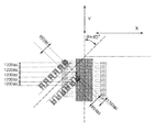
図4−1(a)は、ブラック(BK)インク用の第1の記録素子基板とカラー(CL)インク用の第2の記録素子基板との位置関係、および第2の記録素子基板に配置された電気熱変換素子列の傾斜状態を示す平面図である。また、図4−1(b)に、記録装置上で主走査方向に記録を行ったときに記録されるインクのドットを模式的に示す。 FIG. 4A shows the positional relationship between the first recording element substrate for black (BK) ink and the second recording element substrate for color (CL) ink, and the arrangement on the second recording element substrate. It is a top view which shows the inclination state of the electrothermal conversion element row | line | column made. FIG. 4B schematically illustrates ink dots recorded when recording is performed in the main scanning direction on the recording apparatus.
本実施形態では、図4−1(a),(b)に示すように、第2の記録素子基板H1101上の電気熱変換素子H1103列の一部が主走査方向である矢印X方向に直交する矢印Y方向に対して傾斜角θが45°で傾斜されていることによって、記録時に実質的に解像度2400dpi(dots per inch)で記録を行うことができる記録密度を達成している。図23および図24に示した従来の構成と比較して、本実施形態では、第2の記録素子基板H1101を大幅に大型化させることなく、電気熱変換素子H1103、インク流路の配置密度を比較的低く抑えながら、主走査方向に走査した際の実際の記録密度を高くすることができる。 In the present embodiment, as shown in FIGS. 4A and 4B, a part of the electrothermal transducer elements H1103 row on the second recording element substrate H1101 is orthogonal to the arrow X direction which is the main scanning direction. Since the tilt angle θ is inclined at 45 ° with respect to the direction of the arrow Y, a recording density at which recording can be performed at a resolution of 2400 dpi (dots per inch) is achieved. Compared with the conventional configuration shown in FIG. 23 and FIG. 24, in this embodiment, the arrangement density of the electrothermal conversion element H1103 and the ink flow path is increased without significantly increasing the size of the second recording element substrate H1101. The actual recording density when scanning in the main scanning direction can be increased while keeping it relatively low.
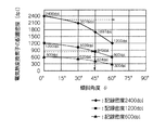
図24に示したように、従来の構成では、せいぜい1200dpi程度であった。この構成に対して延長線上配置の構成のままで2400dpi化するためには、インク流路の幅、仕切壁の幅を平均半分程度に小さくすることが求められていた。その状況に対して本実施形態では、電気熱変換素子列をY方向に対して傾斜角θで傾斜させることによって、図5に示すように、片側の電気熱変換素子列が850dpi程度で、片側の電気熱変換素子列が1200dpi相当(すなわち両側の電気熱変換素子列で2400dpi)が達成することができる。 As shown in FIG. 24, in the conventional configuration, it was about 1200 dpi at most. In order to achieve 2400 dpi while maintaining the configuration on the extended line with respect to this configuration, it has been required to reduce the width of the ink flow path and the width of the partition wall to about an average half. In this embodiment, the electrothermal conversion element array is inclined at an inclination angle θ with respect to the Y direction, so that the electrothermal conversion element array on one side is about 850 dpi, as shown in FIG. The electrothermal conversion element array can be equivalent to 1200 dpi (that is, 2400 dpi for the electrothermal conversion element arrays on both sides).
図5に、Y方向に対する電気熱変換素子列の傾斜角度θ(傾斜角θ=0°が従来の延長線上配置に相当する)と、電気熱変換素子の配置密度(dpi)、との関係を示す。図6に、Y方向に対する電気熱変換素子列の傾斜角度θと、電気熱変換素子の配置ピッチ(μm)との関係を示す。なお、図5および図6において、記録密度(解像度)600dpi,1200dpi,2400dpiの各基準でそれぞれ示す。 FIG. 5 shows the relationship between the inclination angle θ of the electrothermal conversion element array with respect to the Y direction (inclination angle θ = 0 ° corresponds to the arrangement on the conventional extension line) and the arrangement density (dpi) of the electrothermal conversion elements. Show. FIG. 6 shows the relationship between the inclination angle θ of the electrothermal conversion element array with respect to the Y direction and the arrangement pitch (μm) of the electrothermal conversion elements. 5 and 6, the recording densities (resolutions) are 600 dpi, 1200 dpi, and 2400 dpi, respectively.
図5および図6に示すように、従来の延長線上配置(傾斜無し)の構成の場合に、片側の電気熱変換素子列で21.2μmピッチ(1200dpi)であるのに比較して、傾斜角θが45°で傾斜させた構成の場合に30μm程度まで配置密度を緩和して、2400dpiが可能となる。なお、本実施形態では、2400dpiを一例として挙げて説明したが、図5および図6に示したように、電気熱変換素子列がY方向に対して(インク流路のインク流動方向がX方向に対して)傾斜角θが30°〜60°の範囲内で傾斜させて設けられることによって、配置密度を緩和する効果が得られるので、この傾斜角θの範囲内でインク流路の製造実力・製品スペックに応じて電気熱変換素子列・インク流路の配置角度・配置密度を適宜選択すれば良い。 As shown in FIG. 5 and FIG. 6, in the case of the configuration of the conventional extended line arrangement (no inclination), the inclination angle is 21.2 μm pitch (1200 dpi) in the electrothermal transducer array on one side. In the case where θ is inclined at 45 °, the arrangement density is reduced to about 30 μm, and 2400 dpi is possible. In this embodiment, 2400 dpi has been described as an example. However, as illustrated in FIGS. 5 and 6, the electrothermal conversion element array is in the Y direction (the ink flow direction of the ink flow path is the X direction). Since the effect of reducing the arrangement density can be obtained by providing the inclined angle θ within the range of 30 ° to 60 °, the production capability of the ink flow path is within the range of the inclined angle θ. The electrothermal conversion element array, the ink flow path arrangement angle, and the arrangement density may be appropriately selected according to the product specifications.
なお、Y方向に対する電気熱変換素子列の傾斜角θが60°を超える場合には、逆に電気熱変換素子列が主走査方向に(横方向)に延びてしまうので、記録密度を高める一方で、Si基板H1110(記録ヘッド用基板)が大型化し、記録ヘッドの大型化を招いてしまう不都合がある。また、Y方向に対する電気熱変換素子列の傾斜角θが30°未満の場合には、記録密度を充分に高めることができないので、好ましくない。 When the inclination angle θ of the electrothermal conversion element array with respect to the Y direction exceeds 60 °, the electrothermal conversion element array extends in the main scanning direction (horizontal direction). As a result, the Si substrate H1110 (recording head substrate) increases in size, leading to an increase in size of the recording head. In addition, when the inclination angle θ of the electrothermal conversion element array with respect to the Y direction is less than 30 °, it is not preferable because the recording density cannot be sufficiently increased.
次に、本実施形態の記録素子基板について、インク供給口H1102から各電気熱変換素子H1103までの流路の構成、電気熱変換素子列の傾斜配置について、図8および図9を参照して説明する。 Next, regarding the recording element substrate of the present embodiment, the configuration of the flow path from the ink supply port H1102 to each electrothermal conversion element H1103 and the inclined arrangement of the electrothermal conversion element array will be described with reference to FIGS. To do.
図8および図9に示すように、本実施形態の記録素子基板は、Si基板H1110とオリフィスプレートH1111を接合して構成されており、Si基板H1110の厚み方向に貫通して設けられた長溝状のインク供給口H1102と、このインク供給口H1102に連通された共通液室H1112と、この共通液室H1112に連通されたインク導入部H1113と、各電気熱変換素子H1103側に連通されたインク流路H1114と、Y方向に対して傾斜角θを以って傾斜配置された電気熱変換素子列とを備えている。 As shown in FIGS. 8 and 9, the recording element substrate of the present embodiment is configured by bonding a Si substrate H1110 and an orifice plate H1111, and has a long groove shape penetrating in the thickness direction of the Si substrate H1110. Ink supply port H1102, a common liquid chamber H1112 communicated with the ink supply port H1102, an ink introduction part H1113 communicated with the common liquid chamber H1112, and an ink flow communicated with each electrothermal transducer H1103 side. A path H1114 and an electrothermal transducer element array arranged with an inclination angle θ with respect to the Y direction are provided.
記録素子基板のSi基板H1100には、吐出口構成部材であるオリフィスプレートH1111に当接される表面が、平坦面に形成されており、Y方向に対して傾斜された複数の電気熱変換素子列が設けられている。 In the Si substrate H1100 of the recording element substrate, a surface abutting on the orifice plate H1111 which is a discharge port constituting member is formed as a flat surface, and a plurality of electrothermal conversion element arrays inclined with respect to the Y direction. Is provided.
図9に示すように、Si基板H1100に接合されるオリフィスプレートH1111には、インク供給口H1102に対向するとともにインク供給口H1102の開口縁に沿って共通液室H1112が凹設されている。オリフィスプレートH1111には、共通液室H1112に連通されて、Y方向に延長された複数のインク導入部H1113が凹設されている。各インク導入部H1113は、Si基板H1100の主面に平行な平面内で略三角形状をなしており、この三角形の一辺に沿って複数のインク流路H1114の一端がそれぞれ連通されている。各インク導入部H1113に一端が連通された複数のインク流路H1114は、他端が各電気熱変換素子H1103側に延長されて、各電気熱変換素子H1103に対向して設けられた吐出口H1107に連通されている。 As shown in FIG. 9, the orifice plate H1111 bonded to the Si substrate H1100 has a common liquid chamber H1112 that is opposed to the ink supply port H1102 and is recessed along the opening edge of the ink supply port H1102. The orifice plate H1111 has a plurality of ink introduction portions H1113 that are communicated with the common liquid chamber H1112 and extended in the Y direction. Each ink introducing portion H1113 has a substantially triangular shape in a plane parallel to the main surface of the Si substrate H1100, and one end of each of the plurality of ink flow paths H1114 is communicated along one side of the triangle. A plurality of ink flow paths H1114 having one end communicating with each ink introduction portion H1113 is extended to the electrothermal conversion element H1103 side at the other end, and an ejection port H1107 provided to face each electrothermal conversion element H1103. It is communicated to.
本実施形態の構成を従来の構成と比較するために、まず、従来の記録素子基板の構成について簡単に説明する。図23(a)および図24に示したように、従来の記録素子基板では、電気熱変換素子列が、主走査方向に直交するY方向に平行な延長線上に配置された(以下、延長線上配置と称する。)一対の電気熱変換素子列が、インク供給口を間に挟んで対向してそれぞれ配置されている。図24に示したように、従来の記録素子基板では、片側の電気熱変換素子列が解像度600dpiで配置され、両側の電気熱変換素子列で解像度1200dpiをなす構成であり、この構成は問題無く製品化もされている。 In order to compare the configuration of the present embodiment with the conventional configuration, first, the configuration of the conventional recording element substrate will be briefly described. As shown in FIG. 23A and FIG. 24, in the conventional recording element substrate, the electrothermal transducer element array is arranged on an extension line parallel to the Y direction orthogonal to the main scanning direction (hereinafter, on the extension line). A pair of electrothermal conversion element rows are arranged opposite to each other with an ink supply port interposed therebetween. As shown in FIG. 24, in the conventional recording element substrate, the electrothermal conversion element array on one side is arranged with a resolution of 600 dpi, and the electrothermal conversion element array on both sides has a resolution of 1200 dpi. It has also been commercialized.
上述した従来の記録素子基板における電気熱変換素子列の構成に対して、更に記録密度を高めて解像度2400dpiを達成するために、本実施形態の記録素子基板に採用された電気熱変換素子列の構成を以下説明する。 In order to achieve a resolution of 2400 dpi by further increasing the recording density with respect to the configuration of the electrothermal conversion element array in the conventional recording element substrate described above, the electrothermal conversion element array employed in the recording element substrate of this embodiment is used. The configuration will be described below.
図7に、従来の延長線上配置と、この延長線上配置を、Y方向に対して単純に傾斜角を45°だけ傾斜させた傾斜配置との両方について、Y方向に対して片側の電気熱変換素子列が1200dpiピッチとなる配置の平面図をそれぞれ示す。従来の延長線上配置では、図7に示すように、片側の電気熱変換素子列が1200dpiで配列されているが、仕切壁の幅、インク流路の幅が共に狭くなるので、ノズル形成時の精度を考慮すると、歩留まりの低下が避けられない。ここで電気熱変換素子をY方向に対して傾斜角θを45°で傾斜させることで、上述したように850dpi程度で配置可能であり、製造マージンを片側の電気熱変換素子列1200dpiに対してかなり大きく確保することができる。ただし、このままでは、電気熱変換素子列、インク流路、インク供給口等全体が傾斜角45°で傾斜することになり、記録ヘッド全体を傾斜させないと実現が困難であり、記録ヘッド全体を傾斜させた場合に、記録ヘッド全体が大きくなってしまうという問題が発生する。 FIG. 7 shows an electrothermal conversion on one side with respect to the Y direction for both the conventional arrangement on the extension line and the inclination arrangement in which the arrangement on the extension line is simply inclined by 45 ° with respect to the Y direction. A plan view of an arrangement in which element rows are arranged at a 1200 dpi pitch is shown. In the conventional arrangement on the extension line, as shown in FIG. 7, the electrothermal conversion element array on one side is arranged at 1200 dpi, but both the width of the partition wall and the width of the ink flow path are narrowed. In consideration of accuracy, a decrease in yield is inevitable. Here, by inclining the electrothermal conversion element with respect to the Y direction at an inclination angle θ of 45 °, the electrothermal conversion element can be arranged at about 850 dpi as described above, and the manufacturing margin is set to 1200 dpi on one side of the electrothermal conversion element array. It can be secured quite large. However, if the state is kept as it is, the entire electrothermal conversion element array, ink flow path, ink supply port, etc. will be inclined at an inclination angle of 45 °, and this is difficult to achieve unless the entire recording head is inclined. In this case, there arises a problem that the entire recording head becomes large.
図8は、本実施形態の記録素子基板を示す平面図である。図9は、本実施形態の記録素子基板について、図8に示した電気熱変換素子列の配置におけるA−A断面図である。 FIG. 8 is a plan view showing the recording element substrate of the present embodiment. FIG. 9 is a cross-sectional view taken along the line AA in the arrangement of the electrothermal transducer elements shown in FIG. 8 for the recording element substrate of the present embodiment.
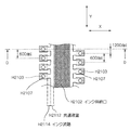
そこで、本実施形態では、図8に示すように、いくつかの電気熱変換素子群に分割し、所定の複数個の電気熱変換素子・インク流路の単位でそれぞれ傾斜させる構成を採用した。具体的には、複数の電気熱変換素子列・インク流路が、Y方向に対して傾斜角θが30°から60°の範囲内で傾斜させると共に、傾斜されている電気熱変換素子列の配列方向に対して、インク流路群のインク流動方向が直交されて、複数の電気熱変換素子列が断続的に配置されるように構成されている。したがって、電気熱変換素子列に連通されたインク流路群は、インク流動方向が主走査方向であるX方向に対して傾斜角θで傾斜されて配置されている。 Therefore, in the present embodiment, as shown in FIG. 8, a configuration is adopted in which it is divided into several electrothermal conversion element groups and inclined in units of a predetermined plurality of electrothermal conversion elements and ink flow paths. Specifically, the plurality of electrothermal conversion element arrays / ink flow paths are inclined with respect to the Y direction within a range of an inclination angle θ of 30 ° to 60 °, and the inclined electrothermal conversion element arrays The ink flow direction of the ink flow path group is orthogonal to the arrangement direction, and the plurality of electrothermal conversion element arrays are intermittently arranged. Therefore, the ink flow path group communicated with the electrothermal conversion element array is disposed at an inclination angle θ with respect to the X direction in which the ink flow direction is the main scanning direction.
図8に示すように、本実施形態の記録素子基板は、インク供給口H1102の形状が、従来の形状と同一形状で、ノズル形成材料のパターニングによってインク供給口H1102の長辺方向の側縁に連通される共通液室H1112が形成されている。このとき、各電気熱変換素子列の傾斜角θに応じて各インク流路H1114の流動方向も傾斜させることで、各電気熱変換素子H1103の主面の中心から、各インク流路H1114のインク導入部H1113側、すなわち上流側の端部までの距離がそれぞれ等しくされると共に、インク流路の仕切壁の幅の製造マージンが大きくなることや、各電気熱変換素子H1103による吐出性能のばらつきを抑えることができる。 As shown in FIG. 8, in the recording element substrate of this embodiment, the shape of the ink supply port H1102 is the same as the conventional shape, and is formed on the side edge in the long side direction of the ink supply port H1102 by patterning the nozzle forming material. A common liquid chamber H1112 that is communicated is formed. At this time, by inclining the flow direction of each ink flow path H1114 according to the inclination angle θ of each electrothermal conversion element array, the ink in each ink flow path H1114 is centered on the main surface of each electrothermal conversion element H1103. The distances to the introduction part H1113 side, that is, the upstream end part are equalized, the manufacturing margin of the width of the partition wall of the ink flow path is increased, and the variation in ejection performance due to each electrothermal conversion element H1103 is caused. Can be suppressed.
ここで、本実施形態の構成と従来の構成とを比較して説明する。図24および図25には、上述の従来の記録素子基板として、両側の電気熱変換素子で1200dpiである電気熱変換素子列を示した。 Here, the configuration of the present embodiment will be described in comparison with the conventional configuration. 24 and 25 show an electrothermal conversion element array having 1200 dpi of electrothermal conversion elements on both sides as the above-described conventional recording element substrate.
図10は、他のインク導入部の構成を変更した他の記録素子基板を示す平面図である。図11は、図10における記録素子基板を示すB−B断面図およびC−C断面図である。なお、他の記録素子基板は、インク導入部、共通液室を除いて上述した記録素子基板と構成が同一であるため、同一部材には同一符号を付して説明を省略する。 FIG. 10 is a plan view showing another recording element substrate in which the configuration of another ink introducing portion is changed. FIGS. 11A and 11B are a BB cross-sectional view and a CC cross-sectional view showing the recording element substrate in FIG. Since the other recording element substrates have the same configuration as the recording element substrate described above except for the ink introduction part and the common liquid chamber, the same members are denoted by the same reference numerals and description thereof is omitted.
本実施形態の記録素子基板では、図10および図11に示すように、図8および図9に示した構成に比較して、上述した共通液室H1112の一部、およびインク導入部H1113の一部が厚み方向に貫通して形成されることで、見かけ上、インク供給口H1102の開口寸法を拡げるように構成されており、共通液室H1122、インク導入部H1123による各電気熱変換素子H1103へのインク供給が更に容易にされている。つまり、この記録素子基板では、共通液室H1122およびインク導入部H1123の一部を厚み方向に貫通して形成されることで、インク供給口H1102の開口形状を変更した構成にされている。 In the recording element substrate of the present embodiment, as shown in FIGS. 10 and 11, compared to the configuration shown in FIGS. 8 and 9, a part of the common liquid chamber H <b> 1112 and one of the ink introduction portions H <b> 1113 described above. The portion is formed so as to penetrate in the thickness direction, so that the opening size of the ink supply port H1102 is apparently expanded, and each electrothermal conversion element H1103 by the common liquid chamber H1122 and the ink introduction portion H1123 is configured. Ink supply is further facilitated. In other words, the recording element substrate has a configuration in which the opening shape of the ink supply port H1102 is changed by forming a part of the common liquid chamber H1122 and the ink introduction portion H1123 in the thickness direction.
上述した記録素子基板の構成は、第2の記録素子基板に適用されている。なお、上述した構成は、必要に応じて第1の記録素子基板にも同様に適用されてもよいことは勿論である。 The configuration of the recording element substrate described above is applied to the second recording element substrate. Of course, the above-described configuration may be similarly applied to the first recording element substrate as needed.
また、第1および第2の記録素子基板に、電気熱変換素子列の傾斜配置の構成を適用する構成の場合、カラーインク用の第2の記録素子基板における電気熱変換素子列の傾斜角を、ブラックインク用の第1の記録素子基板における電気熱変換素子列の傾斜角よりも大きくなるようにされている。このように構成することによって、ブラックインク液滴の大きさは印字スピード重視のため大きく、配列密度(解像度)が低くても済むが、それに対しカラーインクの液滴の大きさは画質重視のため小さくなるので、同じ印字スピードで同じ印字濃度を維持するために解像度を高くする必要がある場合などに効果が得られる。 Further, in the case of applying the configuration in which the electrothermal conversion element array is inclined to the first and second recording element substrates, the inclination angle of the electrothermal conversion element array in the second recording element substrate for color ink is set. The inclination angle of the electrothermal conversion element array in the first recording element substrate for black ink is set to be larger. With this configuration, the size of the black ink droplets is large because printing speed is important, and the arrangement density (resolution) may be low, whereas the color ink droplet size is important because of image quality. Therefore, the effect is obtained when the resolution needs to be increased in order to maintain the same print density at the same print speed.
以下、記録素子基板、Si基板を大型化することなく、電気熱変換素子の配置の高密度化を達成することができる他の実施形態の構成について図面を参照して説明する。なお、他の実施形態において、便宜上、上述の実施形態と同一部材には同一符号を付して説明する。 Hereinafter, the configuration of another embodiment capable of achieving high density of the arrangement of the electrothermal conversion elements without increasing the size of the recording element substrate and the Si substrate will be described with reference to the drawings. In addition, in other embodiment, the same code | symbol is attached | subjected and demonstrated to the same member as the above-mentioned embodiment for convenience.
図12は、他の実施形態の記録素子基板が備える記録ヘッド用基板であるSi基板に設けられたインク供給口と電気熱変換素子配列を模式的に示す平面図である。図12に示すように、本実施形態のSi基板H1110の表面上には、オリフィスプレートH1111側に凹設された共通液室H1112、インク導入部H1113、インク流路H1114、吐出口にそれぞれ対応するように、共通液室H1112の一部、インク導入部H1113、インク流路H1114、電気熱変換素子H1103の周囲に設けられる周壁部H1115がそれぞれ凹設されている。 FIG. 12 is a plan view schematically showing an ink supply port and an electrothermal conversion element array provided on a Si substrate which is a recording head substrate provided in a recording element substrate of another embodiment. As shown in FIG. 12, on the surface of the Si substrate H1110 of this embodiment, it corresponds to a common liquid chamber H1112, an ink introduction part H1113, an ink flow path H1114, and an ejection port that are recessed on the orifice plate H1111 side. As described above, a part of the common liquid chamber H1112, the ink introduction part H1113, the ink flow path H1114, and the peripheral wall part H1115 provided around the electrothermal conversion element H1103 are recessed.
本実施形態の記録素子基板は、従来と同様に長溝状をなすインク供給口H1102に、Si基板H1110の表面側から見てインク供給口H1102の共通液室H1112に連通された凹状のインク導入部H1113を形成することで、このインク導入部H1113がインク供給口H1110のサブ供給口として作用して、このインク導入部H1113からインク流路H1114を介して電気熱変換素子H1103までの流路を引き回す構成にすることで、電気熱変換素子配置の高密度化を達成することが可能にされている。 The recording element substrate of the present embodiment has a concave ink introduction portion that communicates with a common liquid chamber H1112 of the ink supply port H1102 as viewed from the surface side of the Si substrate H1110, in the ink supply port H1102 having a long groove shape as in the conventional case. By forming H1113, the ink introduction part H1113 acts as a sub supply port of the ink supply port H1110, and the flow path from the ink introduction part H1113 to the electrothermal conversion element H1103 through the ink flow path H1114 is routed. With the configuration, it is possible to achieve high density of the electrothermal conversion element arrangement.
図13〜図15に、本実施形態の記録素子基板が備える電気熱変換素子群の具体的な配置例をそれぞれ示す。 FIGS. 13 to 15 show specific arrangement examples of the electrothermal transducer elements provided in the recording element substrate of the present embodiment.
まず、図13(a)に示すように、Si基板H1110は、長溝状のインク供給口H1102の長辺方向の縁部に、長方形状をなす複数のインク導入部H1113が、インク供給口H1102の短辺方向と平行に突出されて凹設されており、インク流路H1114が、各インク導入部H1113から電気熱変換素子H1103側まで引き延ばされて構成されている。そして、各インク流路H1114は、インク導入部H1113に連通する上流側の端部と、電気熱変換素子H1103の主面の中心との間の距離が等しくなるように形成されている。 First, as shown in FIG. 13A, the Si substrate H1110 has a plurality of rectangular ink introduction portions H1113 at the edge of the long-sided ink supply port H1102, and the ink supply port H1102 has a rectangular shape. It protrudes in parallel with the short side direction and is recessed, and the ink flow path H1114 is configured to be extended from each ink introducing portion H1113 to the electrothermal conversion element H1103 side. Each ink flow path H1114 is formed such that the distance between the upstream end communicating with the ink introduction part H1113 and the center of the main surface of the electrothermal conversion element H1103 is equal.
したがって、このSi基板H1110は、インク供給口H1102の長辺方向であるY方向に直交するX方向に対して配列方向が傾斜された複数の電気熱変換素子列を有している。また、各電気熱変換素子H1103の周囲には、インク供給口H1102側から供給されたインクを吐出するための発泡室を構成する周壁部H1115が設けられている。また、図示しないが、共通液室H1112、各インク導入部H1113、各インク流路H1114は、連続して形成されており、Si基板H1110の厚み方向に対する深さが等しく形成されている。 Therefore, this Si substrate H1110 has a plurality of electrothermal conversion element arrays whose arrangement direction is inclined with respect to the X direction orthogonal to the Y direction which is the long side direction of the ink supply port H1102. In addition, a peripheral wall portion H1115 constituting a foaming chamber for discharging ink supplied from the ink supply port H1102 side is provided around each electrothermal conversion element H1103. Although not shown, the common liquid chamber H1112, each ink introducing portion H1113, and each ink flow path H1114 are formed continuously, and the depths in the thickness direction of the Si substrate H1110 are equal.
この構成の場合には、電気熱変換素子H1103の配列密度、電気熱変換素子H1103のレイアウトによっては、図13(a)に示すように、インク導入部H1113を介さずに直接共通液室H1112からインク流路H1114を介してインクが供給されるように電気熱変換素子H1103が配置されても良い。このように共通液室H1112と電気変換素子H1103側との間に配置されるインク流路H1114も同様に、共通液室H1112に連通する上流側の端部と電気熱変換素子H1103の中心との間の距離が、他のインク流路H1114と等しくされている。 In the case of this configuration, depending on the arrangement density of the electrothermal conversion elements H1103 and the layout of the electrothermal conversion elements H1103, as shown in FIG. The electrothermal conversion element H1103 may be arranged so that ink is supplied through the ink flow path H1114. Similarly, the ink flow path H1114 arranged between the common liquid chamber H1112 and the electric conversion element H1103 side similarly has an upstream end communicating with the common liquid chamber H1112 and the center of the electrothermal conversion element H1103. The distance between them is equal to that of the other ink flow paths H1114.
また、図13(b)に示すように、Si基板H1110は、長溝状のインク供給口H1102の長辺方向の縁部に、Si基板H1110の表面上で階段状をなす複数のインク導入部H1113が、インク供給口H1102の短辺方向と平行に突出されて凹設されている。 As shown in FIG. 13B, the Si substrate H1110 has a plurality of ink introduction portions H1113 that form steps on the surface of the Si substrate H1110 at the edge of the long groove-shaped ink supply port H1102. Are protruded in parallel with the short side direction of the ink supply port H1102 and are recessed.
このSi基板H1110は、図13(b)に示すように、階段状をなすインク導入部H1113を備えることで、インク供給口H1102の長辺方向に対して電気熱変換素子H1103を等ピッチで配列する構成に加えて、より一層高密度な配置で、インク流路H1114を上流側から電気熱変換素子H1103の主面の中心までの距離を等しく形成することで、インクの吐出特性を安定化させることができる。 As shown in FIG. 13B, this Si substrate H1110 includes a step-like ink introduction part H1113, so that the electrothermal conversion elements H1103 are arranged at an equal pitch with respect to the long side direction of the ink supply port H1102. In addition to the configuration, the ink flow path H1114 is formed at an even higher density and the distance from the upstream side to the center of the main surface of the electrothermal conversion element H1103 is made equal to stabilize the ink ejection characteristics. be able to.
次に、図14(a),(b)に示すように、Si基板H1110には、Si基板H1110の表面上で階段状をなす複数のインク導入部H1113が形成され、各インク流路H1114の上流側の端部から電気熱変換素子H1103の主面の中心までの距離が等しく形成された構成については、図13(b)に示した構成と同じであるが、本実施形態のSi基板H1110では、各インク導入部H1113の長手方向の一方側縁部にだけインク流路H1114、電気熱変換素子H1103および吐出口H1107が配置されて構成されている。すなわち、各インク導入部H1113は、他方側縁部がインク供給口H1102の短辺方向と平行な直線状に形成されている。 Next, as shown in FIGS. 14A and 14B, the Si substrate H1110 is formed with a plurality of ink introducing portions H1113 that form a step shape on the surface of the Si substrate H1110, and each of the ink flow paths H1114 has a plurality of steps. The configuration in which the distance from the upstream end to the center of the main surface of the electrothermal transducer H1103 is the same is the same as the configuration shown in FIG. 13B, but the Si substrate H1110 of this embodiment. The ink flow path H1114, the electrothermal conversion element H1103, and the ejection port H1107 are arranged only at one side edge in the longitudinal direction of each ink introduction portion H1113. That is, each ink introduction part H1113 is formed in a straight line whose other side edge part is parallel to the short side direction of the ink supply port H1102.
図14(a)に示すように、Si基板H1110には、インク導入部H1113の一方側縁部に沿って電気熱変換素子群が配置されており、各インク導入部H1113の一方側縁部に、X方向に対して傾斜された電気熱変換素子列が配置されている。 As shown in FIG. 14A, the Si substrate H1110 is provided with an electrothermal conversion element group along one side edge of the ink introduction part H1113, and on one side edge of each ink introduction part H1113. The electrothermal conversion element rows inclined with respect to the X direction are arranged.
図14(b)に示すように、Si基板H1110には、インク導入部H1113の一方側縁部に沿って電気熱変換素子群が配置されており、各インク流路H1114のインク流動方向が、インク供給口H1110の短辺方向であるY方向と平行に形成されている。 As shown in FIG. 14B, the Si substrate H1110 has an electrothermal conversion element group arranged along one side edge of the ink introduction part H1113, and the ink flow direction of each ink flow path H1114 is as follows. It is formed in parallel with the Y direction which is the short side direction of the ink supply port H1110.
図13(a),(b)に示したように、インク導入部H1123の長手方向に平行な両側縁部に電気熱変換素子H1103がそれぞれ配置されて対向される構成の場合、インクの吐出およびリフィル時に衝撃波が発生し、その衝撃波によって電気熱変換素子H1103の耐久性が低下してしまい、最悪な場合に電気熱変換素子H1103の接続配線(不図示)が断線してしまう可能性もある。このため、本実施形態の記録素子基板は、図14(a)および図14(b)に示したように、電気熱変換素子H1103を各インク導入部H1113の長手方向の片側縁部のみに配列させることで、インクの吐出およびリフィル時に発生する衝撃波を緩和する効果が得られ、電気熱変換素子H1103の耐久性を確保することができるので好ましい。なお、その他の構成としては、図14(b)に示した構成と類似の構成で、各インク流路H1114を、インク流動方向がX方向と平行に揃えるように構成されてもよい。 As shown in FIGS. 13A and 13B, in the case where the electrothermal conversion elements H1103 are respectively disposed on both side edges parallel to the longitudinal direction of the ink introduction part H1123 and face each other, A shock wave is generated at the time of refilling, and the durability of the electrothermal conversion element H1103 is reduced by the shock wave. In the worst case, the connection wiring (not shown) of the electrothermal conversion element H1103 may be disconnected. Therefore, in the recording element substrate of the present embodiment, as shown in FIGS. 14A and 14B, the electrothermal conversion elements H1103 are arranged only on one side edge portion in the longitudinal direction of each ink introducing portion H1113. By doing so, an effect of mitigating shock waves generated during ink ejection and refilling can be obtained, and durability of the electrothermal conversion element H1103 can be ensured, which is preferable. As other configurations, the configuration similar to the configuration illustrated in FIG. 14B may be configured such that the ink flow paths H1114 are aligned in parallel with the X direction.
図15(a),(b)に示すように、Si基板H1110は、図13および図14に示した構成に比較して、長溝状のインク供給口H1102の長辺方向の縁部に、Si基板H1110の表面上で三角形状をなす複数のインク導入部H1113が、インク供給口H1102の短辺方向と平行に突出されて凹設されている点が異なる。 As shown in FIGS. 15A and 15B, the Si substrate H1110 has an Si groove H1110 at the edge in the long side direction of the long groove-shaped ink supply port H1102 as compared with the configuration shown in FIGS. A different point is that a plurality of ink introducing portions H1113 having a triangular shape on the surface of the substrate H1110 are protruded and recessed in parallel with the short side direction of the ink supply port H1102.
また、インク流路H1114は、各インク導入部H1113から電気熱変換素子H1103側まで引き延ばされて構成されている。そして、各インク流路H1114は、図8および図9に示した実施形態に比較して、下流側端部が、発泡室を構成する周壁部H1115の角部に連通されている。 Further, the ink flow path H1114 is configured to be extended from each ink introduction portion H1113 to the electrothermal conversion element H1103 side. Each of the ink flow paths H1114 is communicated with a corner portion of the peripheral wall H1115 constituting the foaming chamber, as compared with the embodiment shown in FIGS. 8 and 9.
このような構成によれば、図13および図14に示した構成と同様に、電気熱変換素子H1103の配置の高密度化が図られ、電気熱変換素子H1103および吐出口の高密度配置を達成することが可能である。 According to such a configuration, similarly to the configurations shown in FIGS. 13 and 14, the arrangement of the electrothermal conversion elements H <b> 1103 is increased in density, and the high density arrangement of the electrothermal conversion elements H <b> 1103 and the discharge ports is achieved. Is possible.
以上のように様々な構成が考えられるが、インク供給口H1110の長辺方向の縁部に複数のインク導入部H1113が形成されて、いずれの構成においても、その各インク導入部H1113に複数の電気熱変換素子H1103が配置されることで、電気熱変換素子配列の高密度化を達成することが可能になる。また、インク供給口H1110(インク導入部H1113の端部も含む)端部から電気熱変換素子H1103の主面の中心までの距離がほぼ等しくなるように構成されることで、Si基板H1110内の電気熱変換素子H1103毎における吐出の安定化も同時に達成することができる。 As described above, various configurations are conceivable. A plurality of ink introduction portions H1113 are formed at the edge in the long side direction of the ink supply port H1110. In any configuration, a plurality of ink introduction portions H1113 are provided in each of the ink introduction portions H1113. By disposing the electrothermal conversion element H1103, it is possible to achieve high density of the electrothermal conversion element array. In addition, since the distance from the end of the ink supply port H1110 (including the end of the ink introduction part H1113) to the center of the main surface of the electrothermal transducer H1103 is substantially equal, Stabilization of ejection for each electrothermal transducer H1103 can also be achieved at the same time.
次に、更に他の実施形態の記録素子基板について図面を参照して説明する。図16〜図18は、更に他の実施形態に係る電気熱変換素子群の具体的な配置例を示す図である。 Next, a recording element substrate of still another embodiment will be described with reference to the drawings. FIGS. 16-18 is a figure which shows the specific example of arrangement | positioning of the electrothermal conversion element group which concerns on further another embodiment.
図16〜図18に示すように、本実施形態の記録素子基板は、インク供給口、共通液室およびインク導入部の構成が図13〜図15に示した各構成とそれぞれ同一であるが、図13〜図15に示した構成と比較して、主面である発熱面積の大きさ(ヒータサイズ)が異なる複数種の電気熱変換素子H1103a〜H1103dと、発泡室内に向かう流動方向に直交する幅が異なる複数種のインク流路H1114a〜H1114dとを備えている。 As shown in FIGS. 16 to 18, the recording element substrate of the present embodiment has the same configuration of the ink supply port, the common liquid chamber, and the ink introduction unit as the respective configurations shown in FIGS. 13 to 15. Compared to the configurations shown in FIGS. 13 to 15, the electrothermal transducers H1103a to H1103d having different heat generation area sizes (heater sizes) as the main surface are orthogonal to the flow direction toward the foaming chamber. A plurality of types of ink flow paths H1114a to H1114d having different widths are provided.
この記録素子基板は、各電気熱変換素子H1103a〜H1103dに対応する吐出口の開口面積、各発泡室の大きさ、およびインク流路H1114の幅もそれぞれ異なっており、インク供給口H1110の長辺方向の側縁から離間するのに従って、電気熱変換素子H1103、吐出口、インク流路H1114の幅、発泡室等が順次に大きくなるように配置されて構成されている。図示しないが、オリフィスプレートH1111には、各電気熱変換素子H1103a〜H1103dに対応して、開口面積が異なる吐出口がそれぞれ形成されている。すなわち、本実施形態の記録素子基板は、吐出口群が異なる大きさのインク滴をそれぞれ吐出(マルチドロップ化)するように構成されている。 In this recording element substrate, the opening area of the discharge port corresponding to each of the electrothermal conversion elements H1103a to H1103d, the size of each foaming chamber, and the width of the ink flow path H1114 are also different, and the long side of the ink supply port H1110 The electrothermal conversion element H1103, the ejection port, the width of the ink flow path H1114, the foaming chamber, and the like are arranged so as to increase sequentially as the distance from the side edge in the direction increases. Although not shown, the orifice plate H1111 is formed with discharge ports having different opening areas corresponding to the electrothermal transducers H1103a to H1103d. In other words, the recording element substrate of the present embodiment is configured to discharge (multi-drop) ink droplets having different sizes from each other.
このように構成することによって、電気熱変換素子の高密度配置と、大きさが異なる複数種類の電気熱変換素子を配置することによるマルチドロップ化との両立が可能になり、更なる高画質化、および記録速度の高速化を図ることが可能になる。 By configuring in this way, it is possible to achieve both high-density arrangement of electrothermal conversion elements and multi-drop by arranging multiple types of electrothermal conversion elements with different sizes, further improving image quality It is possible to increase the recording speed.
更に他の実施形態の記録素子基板について図面を参照して説明する。図19〜図21は、更に他の実施形態に係る電気熱変換素子群の具体的な配置例を示す図である。 Further, a recording element substrate according to another embodiment will be described with reference to the drawings. FIGS. 19-21 is a figure which shows the specific example of arrangement | positioning of the electrothermal conversion element group which concerns on further another embodiment.
図19〜図21に示すように、本実施形態の記録素子基板は、第1の実施形態と同様に、主面の大きさが同一の電気熱変換素子群を高密度に配置した構成である。本実施形態の記録素子基板は、図10および図11に示した実施形態と同様に、共通液室H1122およびインク導入部H1123が、Si基板H1110の厚み方向に対して裏面側まで貫通して形成されており、インク供給口H1102に連続して形成されている。 As shown in FIGS. 19 to 21, the recording element substrate of the present embodiment has a configuration in which electrothermal transducer elements having the same main surface size are arranged at high density, as in the first embodiment. . As in the embodiment shown in FIGS. 10 and 11, the recording element substrate of the present embodiment is formed such that the common liquid chamber H1122 and the ink introduction portion H1123 penetrate to the back side with respect to the thickness direction of the Si substrate H1110. It is formed continuously to the ink supply port H1102.
このような共通液室H1122、インク導入部H1123は、上述したインク供給口H1102の形成時に、インク供給口H1102と同時に、共通液室H1122、インク導入部H1123もエッチングを行うことで、インク供給口H1102と同様に貫通されて形成されている。 Such a common liquid chamber H1122 and the ink introduction part H1123 are also etched with the common liquid chamber H1122 and the ink introduction part H1123 simultaneously with the ink supply opening H1102 when the ink supply opening H1102 is formed. Like H1102, it is formed to penetrate.
以上、図12〜図21を用いて説明した他の実施形態について、図4―1,図5〜図11で説明したように、電気熱変換素子をY方向に対して30°〜60°の傾斜角θで傾斜させて配置することは、製造マージンを確保できる点で望ましい。 As described above with reference to FIGS. 4-1 and FIGS. 5 to 11, the other embodiments described with reference to FIGS. It is desirable to dispose at an inclination angle θ because a manufacturing margin can be secured.
また、以上説明してきた各実施形態では、吐出口の配列は、Y方向と平行な軸に対して略対称となっている。しかしながら、図4−1,図5〜図11で説明した電気熱変換素子をY方向に対して30°〜60°の傾斜角θで傾斜させて配置することについては、このような構成、及びインク供給口とインク流路との間に複数のインク導入部を設ける構成は必須ではなく、例えば図4−2(a)、(b)に示すような配置であっても良い。この配置では、図4−2(a)に示すように、複数の記録素子およびインク流路が、記録ヘッドの走査方向に垂直な方向(Y方向)に対して傾斜角θで傾斜されていると共に、傾斜角θが30°から60°の範囲にあり、さらに傾斜されている記録素子群とインク流路群が記録ヘッドの走査方向に垂直な方向(Y方向)に対して断続的に配置されている。 In each of the embodiments described above, the arrangement of the discharge ports is substantially symmetric with respect to an axis parallel to the Y direction. However, with respect to the arrangement of the electrothermal conversion elements described in FIGS. 4A and 1B and FIGS. 5 to 11 with an inclination angle θ of 30 ° to 60 ° with respect to the Y direction, such a configuration, and A configuration in which a plurality of ink introducing portions are provided between the ink supply port and the ink flow path is not essential, and for example, an arrangement as shown in FIGS. 4-2 (a) and (b) may be employed. In this arrangement, as shown in FIG. 4A, the plurality of recording elements and ink flow paths are inclined at an inclination angle θ with respect to a direction (Y direction) perpendicular to the scanning direction of the recording head. In addition, the inclination angle θ is in the range of 30 ° to 60 °, and the inclined recording element group and the ink flow path group are intermittently arranged in the direction (Y direction) perpendicular to the scanning direction of the recording head. Has been.
また、図示しないが、他の実施形態の構成としては、図16〜図18に示した実施形態のように各電気熱変換素子H1103、インク流路H1114の幅等を異ならせることでマルチドロップ化および電気熱変換素子H1103の高密度配置を共に実現する構成に、本実施形態のようにインク供給口H1110と同様に厚み方向に貫通された共通液室H1122、インク導入部H1123を備える構成が組み合わせてもよいことは勿論である。 Although not shown in the drawings, the configuration of another embodiment is multidrop by changing the width of each electrothermal conversion element H1103 and ink flow path H1114 as in the embodiment shown in FIGS. In addition to the configuration that realizes the high-density arrangement of the electrothermal conversion elements H1103, the configuration including the common liquid chamber H1122 and the ink introduction portion H1123 that are penetrated in the thickness direction as in the case of the ink supply port H1110 is combined. Of course, it may be.
次に、記録ヘッドが備える第1のプレートH1200は、例えば、厚さ0.5〜10mm程度のアルミナ(Al2O3)材料で形成されている。なお、第1のプレートH1200の材料としては、アルミナに限定されることなく、第1の記録素子基板H1100をなす材料の線膨張率と同等の線膨張率を有し、かつ、第1の記録素子基板H1100をなす材料の熱伝導率と同等以上の熱伝導率を有する材料によって形成されてもよい。第1のプレートH1200の材料としては、例えば、シリコン(Si)、窒化アルミニウム(AlN)、ジルコニア、窒化珪素(Si3N4)、炭化珪素(SiC)、モリブデン(Mo)、タングステン(W)のうちのいずれであってもよい。 Next, the first plate H1200 included in the recording head is made of, for example, an alumina (Al 2 O 3 ) material having a thickness of about 0.5 to 10 mm. The material of the first plate H1200 is not limited to alumina, and has a linear expansion coefficient equivalent to the linear expansion coefficient of the material forming the first recording element substrate H1100 and the first recording element H1200. It may be formed of a material having a thermal conductivity equal to or higher than the thermal conductivity of the material forming the element substrate H1100. Examples of the material of the first plate H1200 include silicon (Si), aluminum nitride (AlN), zirconia, silicon nitride (Si 3 N 4 ), silicon carbide (SiC), molybdenum (Mo), and tungsten (W). Any of them may be used.
図2に示したように、第1のプレートH1200には、第1の記録素子基板H1100にブラックインクを供給するためのインク供給口H1201aと、第2の記録素子基板H1101にシアン、マゼンタ、イエローのカラーインクを供給するためのインク供給口H1201bがそれぞれ形成されている。第1のプレートH1200には、インク供給口H1201aに対して第1の記録素子基板H1100のインク供給口H1102が位置決めされ、またインク供給口H1201bに対して第2の記録素子基板H1101のインク供給口H1102が位置決めされて、接着により固定されている。接着に用いられる第1の接着剤としては、低粘度で硬化温度が低く、短時間で硬化し、硬化後比較的高い硬度を有し、かつ、耐インク性を有するものが望ましい。このような第1の接着剤は、例えば、エポキシ樹脂を主成分とした熱硬化接着剤であり、この第1の接着層の厚みは50μm以下が望ましい。 As shown in FIG. 2, the first plate H1200 has an ink supply port H1201a for supplying black ink to the first recording element substrate H1100, and cyan, magenta, and yellow for the second recording element substrate H1101. Ink supply ports H1201b for supplying the color ink are formed. In the first plate H1200, the ink supply port H1102 of the first recording element substrate H1100 is positioned with respect to the ink supply port H1201a, and the ink supply port of the second recording element substrate H1101 with respect to the ink supply port H1201b. H1102 is positioned and fixed by adhesion. The first adhesive used for bonding is desirably a low viscosity, low curing temperature, cured in a short time, has a relatively high hardness after curing, and has ink resistance. Such a first adhesive is, for example, a thermosetting adhesive mainly composed of an epoxy resin, and the thickness of the first adhesive layer is desirably 50 μm or less.
電気配線テープH1300は、第1の記録素子基板H1100と第2の記録素子基板H1101に対して、インクを吐出するための電気信号を印加するためのものである。この電気配線テープH1300は、各第1および第2の記録素子基板H1100,H1101を組み込むための2つの開口部と、各第1および第2の記録素子基板H1100,H1101の電極H1104に対応する電極端子(不図示)と、この電気配線テープH1300の端部に設けられて記録装置側からの電気信号を受け取るための外部信号入力端子H1301とを有する電気コンタクト基板H2200に電気的に接続するための電極端子部を有している。この電極端子部と電極リード(不図示)は、連続した銅箔の配線パターンでつながっている。この電気配線テープH1300は、例えば、配線が2層構造をなし、表層がレジストフィルムによって覆われているフレキシブル配線基板からなる。このフレキシブル配線基板の場合、外部信号入力端子H1301の裏面側(外面側)には、補強板(不図示)が接着され、平面性の向上が図られている。補強板としては、例えば0.5〜2mm程度のガラスエポキシ、アルミニウム等の耐熱性を有する材料が使用される。 The electrical wiring tape H1300 is for applying an electrical signal for ejecting ink to the first recording element substrate H1100 and the second recording element substrate H1101. The electrical wiring tape H1300 includes two openings for incorporating the first and second recording element substrates H1100 and H1101, and electrodes corresponding to the electrodes H1104 of the first and second recording element substrates H1100 and H1101. Electrically connected to an electrical contact substrate H2200 having terminals (not shown) and an external signal input terminal H1301 provided at an end of the electrical wiring tape H1300 for receiving an electrical signal from the recording apparatus side It has an electrode terminal part. The electrode terminal portion and the electrode lead (not shown) are connected by a continuous wiring pattern of copper foil. The electrical wiring tape H1300 is made of, for example, a flexible wiring board in which the wiring has a two-layer structure and the surface layer is covered with a resist film. In the case of this flexible wiring board, a reinforcing plate (not shown) is bonded to the back surface side (outer surface side) of the external signal input terminal H1301 to improve the flatness. As the reinforcing plate, for example, a material having heat resistance such as glass epoxy or aluminum of about 0.5 to 2 mm is used.
電気配線テープH1300と第1の記録素子基板H1100と第2の記録素子基板H1101は、それぞれ電気的に接続されている。接続方法としては、例えば、記録素子基板の電極H1104上のバンプH1105と、電気配線テープH1300の電極リードとが、熱超音波圧着法により電気的に接合される。 The electrical wiring tape H1300, the first recording element substrate H1100, and the second recording element substrate H1101 are electrically connected to each other. As a connection method, for example, the bump H1105 on the electrode H1104 of the recording element substrate and the electrode lead of the electric wiring tape H1300 are electrically joined by a thermosonic bonding method.
第2のプレートH1400は、例えば、厚さ0.5〜1mm程度の1枚の板状部材であり、例えばアルミナ(Al2O3)等のセラミックや、Al、SUS等の金属材料で形成されている。なお、第2のプレートH1400の材料としては、これらに限定されるものではなく、各第1および第2の記録素子基板H1100,H1101、第1のプレートH1200と同等の線膨張率を有し、かつ、これらの熱伝導率と同等以上の熱伝導率を有する材料であってもよい。 The second plate H1400 is, for example, a single plate-like member having a thickness of about 0.5 to 1 mm, and is formed of a ceramic material such as alumina (Al 2 O 3 ) or a metal material such as Al or SUS. ing. The material of the second plate H1400 is not limited to these, and has a linear expansion coefficient equivalent to that of each of the first and second recording element substrates H1100, H1101, and the first plate H1200. Moreover, a material having a thermal conductivity equal to or higher than these thermal conductivities may be used.
そして、第2のプレートH1400には、第1のプレートH1200に接着されて固定された第1の記録素子基板H1100と第2の記録素子基板H1101の外形寸法よりも大きな各開口部がそれぞれ設けられている。また、第1の記録素子基板H1100および第2の記録素子基板H1101と電気配線テープH1300とを平面的に電気的に接続できるように、第1のプレートH1200に第2の接着剤層により接着されており、電気配線テープH1300の裏面が第3の接着剤層により接着固定される。 The second plate H1400 is provided with openings that are larger than the outer dimensions of the first recording element substrate H1100 and the second recording element substrate H1101 that are bonded and fixed to the first plate H1200. ing. Further, the first recording element substrate H1100 and the second recording element substrate H1101 and the electric wiring tape H1300 are bonded to the first plate H1200 with a second adhesive layer so that they can be electrically connected in a plane. The back surface of the electrical wiring tape H1300 is bonded and fixed by the third adhesive layer.
第1の記録素子基板H1100および第2の記録素子基板H1101と電気配線テープH1300との電気的な各接続部分は、第1および第2の封止剤(不図示)によってそれぞれ封止されており、各接続部分をインクによる腐食や外的衝撃から保護されている。第1の封止剤は、主に電気配線テープH1300の電極端子と記録素子基板H1100,H1101のバンプH1105との接続部分の裏面側と、記録素子基板H1100,H1101の外周部分をそれぞれ封止し、第2の封止剤は、接続部分の表面側を封止している。 The electrical connection portions of the first recording element substrate H1100 and the second recording element substrate H1101 and the electric wiring tape H1300 are respectively sealed with first and second sealing agents (not shown). Each connection is protected from ink corrosion and external impact. The first sealant mainly seals the back side of the connection portion between the electrode terminal of the electric wiring tape H1300 and the bump H1105 of the recording element substrates H1100 and H1101 and the outer peripheral portion of the recording element substrates H1100 and H1101. The second sealant seals the surface side of the connection portion.
さらに、電気配線テープH1300の端部に記録装置側からの電気信号を受け取るための外部信号入力端子H1301を有する電気コンタクト基板H2200が、異方性導電フィルム等を用いて熱圧着され電気的に接続されている。 Furthermore, an electrical contact substrate H2200 having an external signal input terminal H1301 for receiving an electrical signal from the recording apparatus side at the end of the electrical wiring tape H1300 is thermocompression-bonded and electrically connected using an anisotropic conductive film or the like. Has been.
そして、電気配線テープH1300は、第2のプレートH1400に接着されると同時に、第1のプレートH1200および第2のプレートH1400の一側面に沿って折り曲げられ、第1のプレートH1200の側面に第3の接着層(不図示)によって接着される。第2の接着剤は、粘度が比較的低く、接触面に比較的薄い第2の接着層H1203を形成し得るとともに、耐インク性を有するものが好ましい。また、第3の接着層は、例えば、エポキシ樹脂を主成分とした厚さ100μm以下の熱硬化接着剤層である。 The electric wiring tape H1300 is bonded to the second plate H1400, and at the same time is bent along one side of the first plate H1200 and the second plate H1400. Are adhered by an adhesive layer (not shown). The second adhesive preferably has a relatively low viscosity, can form a relatively thin second adhesive layer H1203 on the contact surface, and has ink resistance. The third adhesive layer is, for example, a thermosetting adhesive layer having an epoxy resin as a main component and a thickness of 100 μm or less.
[1−2] インク供給ユニット
インク供給部材H1500は、例えば、樹脂成形により形成されている。この樹脂材料には、形状的剛性を向上させるためにガラスフィラーを5〜40%程度混入した樹脂材料を使用することが望ましい。
[1-2] Ink Supply Unit The ink supply member H1500 is formed by resin molding, for example. As this resin material, it is desirable to use a resin material mixed with about 5 to 40% of glass filler in order to improve the shape rigidity.
図1、図2に示すように、インクタンクH1900を着脱自在に保持するインク供給部材H1500は、インクタンクH1900から記録素子ユニットH1002にインクを導くためのインク供給ユニットH1003の一構成部品であり、流路形成部材H1600が超音波溶着されて、インクタンクH1900から第1のプレートH1200に至るインク供給路H1501が形成されている。また、インクタンクH1900に係合されるジョイント部には、外部から塵埃が進入することを防ぐためのフィルタH1700が溶着によって接合されており、さらに、ジョイント部からインクが蒸発することを防止するためのシールゴムH1800が組み込まれている。 As shown in FIGS. 1 and 2, the ink supply member H1500 that detachably holds the ink tank H1900 is a component of the ink supply unit H1003 for guiding ink from the ink tank H1900 to the recording element unit H1002. The flow path forming member H1600 is ultrasonically welded to form an ink supply path H1501 from the ink tank H1900 to the first plate H1200. Further, a filter H1700 for preventing dust from entering from the outside is joined to the joint portion engaged with the ink tank H1900 by welding, and further, ink is prevented from evaporating from the joint portion. The seal rubber H1800 is incorporated.
また、インク供給ユニットH1003は、記録ヘッドカートリッジH1000を記録装置側のキャリッジの装着位置に案内するための装着ガイドH1601と、記録ヘッドカートリッジH1000をヘッドセットレバーによりキャリッジに装着固定するための係合部と、キャリッジの所定の装着位置に位置決めするための主走査方向であるX方向(キャリッジスキャン方向)の突き当て部H1509と、Y方向(被記録材の搬送方向)の突き当て部H1510と、Z方向(インク吐出方向)の突き当て部H1511とを備えている。また、インク供給ユニットH1003は、記録素子ユニットH1002の電気コンタクト基板H2200を位置決めして固定する端子固定部H1512を有している。端子固定部H1512およびその周囲には、複数のリブが設けられており、端子固定部H1512を有する面の剛性を高めている。 The ink supply unit H1003 includes a mounting guide H1601 for guiding the recording head cartridge H1000 to the mounting position of the carriage on the recording apparatus side, and an engaging portion for mounting and fixing the recording head cartridge H1000 on the carriage by a head set lever. An abutting portion H1509 in the X direction (carriage scanning direction) that is the main scanning direction for positioning at a predetermined mounting position of the carriage, an abutting portion H1510 in the Y direction (recording material conveyance direction), and Z And an abutting portion H1511 in the direction (ink discharge direction). The ink supply unit H1003 has a terminal fixing portion H1512 that positions and fixes the electrical contact substrate H2200 of the recording element unit H1002. A plurality of ribs are provided around the terminal fixing portion H1512 and its periphery to enhance the rigidity of the surface having the terminal fixing portion H1512.
[1−3] 記録素子ユニットとインク供給ユニットの結合
上述の図2に示したように、記録ヘッドH1001は、記録素子ユニットH1002をインク供給ユニットH1003に結合し、さらにタンクホルダH2000と結合することにより完成する。結合は以下のように行われる。
[1-3] Coupling of Recording Element Unit and Ink Supply Unit As shown in FIG. 2 described above, the recording head H1001 connects the recording element unit H1002 to the ink supply unit H1003 and further to the tank holder H2000. To complete. The coupling is performed as follows.
記録素子ユニットH1002のインク供給口(第1のプレートH1200のインク供給口H1201)とインク供給ユニットH1003のインク供給口(流路形成部材H1600のインク供給穴H1602)とを、インクが漏洩しないように連結させるために、ジョイントシール部材H2300を介してそれぞれの部材を圧着するようビスH2400で固定する。このとき、記録素子ユニットH1002は、インク供給ユニットH1003のX方向、Y方向、およびZ方向の各基準位置に対して高精度に位置決めされ固定される。 Ink does not leak through the ink supply port of the recording element unit H1002 (ink supply port H1201 of the first plate H1200) and the ink supply port of the ink supply unit H1003 (ink supply hole H1602 of the flow path forming member H1600). In order to make the connection, each member is fixed with a screw H2400 so as to be pressure-bonded via a joint seal member H2300. At this time, the recording element unit H1002 is positioned and fixed with high accuracy with respect to the reference positions of the ink supply unit H1003 in the X direction, the Y direction, and the Z direction.
そして、記録素子ユニットH1002の電気コンタクト基板H2200は、インク供給部材H1500の一側面に、端子位置決めピン(2ヶ所)と端子位置決め穴(2ヶ所)とによって位置決めされて固定される。固定方法としては、例えば、インク供給部材H1500に設けられた端子位置決めピンをかしめることにより固定されるが、その他の固定手段を用いて固定されても良い。 The electrical contact substrate H2200 of the recording element unit H1002 is positioned and fixed to one side surface of the ink supply member H1500 by terminal positioning pins (2 locations) and terminal positioning holes (2 locations). As a fixing method, for example, fixing is performed by caulking a terminal positioning pin provided in the ink supply member H1500, but the fixing may be performed using other fixing means.
さらに、インク供給部材H1500のタンクホルダとの結合穴および結合部をタンクホルダH2000に嵌合させ結合することにより、記録ヘッドH1001が完成する。すなわち、インク供給部材H1500、流路形成部材H1600、フィルタH1700、シールゴムH1800から構成されるタンクホルダ部と、記録素子基板H1100,H1101、第1のプレートH1200、配線基板H1300、第2のプレートH1400から構成される記録素子部とを接着等で結合することにより、記録ヘッドH1001が構成されている。 Further, the recording head H1001 is completed by fitting and coupling the coupling hole and coupling portion of the ink supply member H1500 with the tank holder to the tank holder H2000. That is, from the tank holder portion composed of the ink supply member H1500, the flow path forming member H1600, the filter H1700, and the seal rubber H1800, the recording element substrates H1100 and H1101, the first plate H1200, the wiring substrate H1300, and the second plate H1400. The recording head H1001 is configured by joining the configured recording element unit by bonding or the like.
[2] 記録ヘッドカートリッジ
上述のように、インクタンクH1900の各タンク部内には、対応する各色のインクがそれぞれ収容されている。また、インクタンクH1900の各タンク部には、タンク部内のインクを記録ヘッドH1001に供給するためのインク供給口(不図示)が形成されている。インクタンクH1900は、記録ヘッドH1001に装着されたとき、インク供給口が記録ヘッドH1001側のジョイント部に設けられたフィルタH1700に圧接され、各タンク部内のインクが、インク供給口から記録ヘッドH1001のインク供給路H1501を介して第1のプレートH1200を経て第1の記録素子基板H1100に供給される。
[2] Recording Head Cartridge As described above, each color ink is stored in each tank portion of the ink tank H1900. Each tank portion of the ink tank H1900 is formed with an ink supply port (not shown) for supplying ink in the tank portion to the recording head H1001. When the ink tank H1900 is mounted on the recording head H1001, the ink supply port is pressed against a filter H1700 provided in the joint portion on the recording head H1001 side, and the ink in each tank portion is transferred from the ink supply port to the recording head H1001. The ink is supplied to the first recording element substrate H1100 via the ink supply path H1501 and the first plate H1200.
そして、第1の記録素子基板H1100に供給されたインクは、各インク流路の端部に配置され電気熱変換素子H1103および吐出口H1107を有する発泡室内に供給され、電気熱変換素子H1103から与えられる熱エネルギーによってインク滴として記録用紙等の被記録材に向けて吐出される。 The ink supplied to the first recording element substrate H1100 is supplied to the foam chamber having the electrothermal conversion element H1103 and the discharge port H1107 disposed at the end of each ink flow path, and is supplied from the electrothermal conversion element H1103. The ink is ejected as ink droplets toward a recording material such as recording paper by the heat energy.
[3] インクジェット記録装置
上述したようなカートリッジタイプの記録ヘッドH1001を搭載可能な記録装置について説明する。図22は、上述した本実施形態の記録ヘッドを搭載可能な記録装置の一例を示す平面図である。
[3] Inkjet recording apparatus A recording apparatus capable of mounting the cartridge type recording head H1001 as described above will be described. FIG. 22 is a plan view showing an example of a recording apparatus in which the recording head of this embodiment described above can be mounted.
図22に示すように、記録装置には、図1に示した記録ヘッドカートリッジH1000がキャリッジ102に位置決めされて交換可能に搭載されている。キャリッジ102には、記録ヘッドカートリッジH1000上の外部信号入力端子を介して各吐出部に駆動信号等を伝達するための電気接続部が設けられている。
As shown in FIG. 22, in the recording apparatus, the recording head cartridge H1000 shown in FIG. The
キャリッジ102は、主走査方向に延在して記録装置内部に設置されたガイドシャフト103の軸方向に沿ってX方向に往復移動可能に案内支持されている。そして、キャリッジ102は、主走査モータ104によってモータプーリ105、従動プーリ106およびタイミングベルト107等の駆動機構を介して駆動されるとともに、その位置および移動が制御される。また、キャリッジ102には、ホームポジションセンサ130が設けられており、遮蔽板136の位置をキャリッジ102上のホームポジションセンサ130が通過した際に、キャリッジ102の位置を検知することが可能にされている。
The
記録用紙やプラスチック薄板等の被記録材108は、給紙モータ135によってギアを介して給紙ローラ131を回転させることによって、オートシートフィーダ(ASF)132からY方向に一枚ずつ分離給紙される。さらに、搬送ローラ109が回転駆動されることによって、被記録材108は、記録ヘッドカートリッジH1000の吐出口面と対向する記録位置を通って搬送される。搬送ローラ109は、LF(ラインフィード)モータ134が回転駆動されることによってギアを介して駆動力が伝達される。その際、被記録材108が給紙されたか否かの判定と給紙時の被記録材108の前端位置の確定は、ペーパエンドセンサ133を被記録材108が通過した時点で行われる。さらに、ペーパエンドセンサ133は、被記録材108の後端が実際にどの位置にあり、実際の後端から現在の記録位置を最終的に割り出すためにも使用される。
The
なお、被記録材108は、記録位置において平坦な被記録面を構成するように、その裏面がプラテン(不図示)によって支持されている。この場合、キャリッジ102に搭載された記録ヘッドカートリッジH1000は、それらの吐出口面がキャリッジ102から下方へ突出されて、搬送ローラ109対の間で被記録材108と平行になるように保持されている。
Note that the back surface of the
記録ヘッドカートリッジH1000は、各記録素子基板における吐出口列の配列方向が、上述したキャリッジ102の走査方向に直交する方向に対して所定の傾斜角θを以って交差するように、キャリッジ102に搭載され、これらの吐出口列からインクを吐出して記録を行う。
The recording head cartridge H1000 is disposed on the
また、記録装置は、記録ヘッドカートリッジH1000に対して電気熱変換素子を駆動するための駆動信号やその他の信号を供給するための信号供給部、および電源供給部を備えている。 The recording apparatus also includes a signal supply unit for supplying a drive signal and other signals for driving the electrothermal transducer to the recording head cartridge H1000, and a power supply unit.
そして、本実施形態の記録装置によれば、カラーインクによる主走査方向に直交する方向であるY方向に対する実質上の記録密度が、図4−1(b)に示すように、2400dpiを達成することができる。 According to the recording apparatus of the present embodiment, the actual recording density in the Y direction, which is the direction orthogonal to the main scanning direction, is 2400 dpi as shown in FIG. 4B. be able to.
H1100 第1の記録素子基板
H1101 第2の記録素子基板
H1102 インク供給口
H1103 電気熱変換素子(記録素子)
H1107 吐出口
H1110 Si基板
H1111 オリフィスプレート(吐出口構成部材)
H1112 共通液室
H1113 インク導入部
H1114 インク流路
H1100 First recording element substrate H1101 Second recording element substrate H1102 Ink supply port H1103 Electrothermal conversion element (recording element)
H1107 Discharge port H1110 Si substrate H1111 Orifice plate (Discharge port component)
H1112 Common liquid chamber H1113 Ink introduction part H1114 Ink flow path
Claims (7)
複数の前記電気熱変換素子の各々に対応する複数の吐出口と、前記液体供給口からの液体を前記吐出口へ供給する、壁によって仕切られた複数の液体流路と、を備える吐出口形成部材と、
を有し、被記録材に対して走査方向に走査される液体吐出ヘッドにおいて、
前記液体供給口の側縁にて前記液体供給口と連通された共通液室と、複数の前記液体流路と前記共通液室とを連通する複数の液体導入部とが構成され、
前記液体導入部は、複数の前記液体流路にそれぞれ連通され、
前記電気熱変換素子群における各々の前記電気熱変換素子の配列方向は、前記走査方向と直交する方向に対して30゜から60゜の範囲内の第1の傾斜角で傾斜され、前記電気熱変換素子群に対応する各々の前記液体流路の液体の流動方向は、前記走査方向に対して30゜から60゜の範囲内の第2の傾斜角で傾斜されていることを特徴とする液体吐出ヘッド。 An electrothermal conversion element that generates thermal energy for discharging the liquid, and a liquid supply port that is provided through the thickness direction to supply the liquid from the back surface to the electrothermal conversion element side on the surface, a base plate configured multiple electrothermal conversion element group are a plurality of said electrothermal converting element is arranged,
A discharge port forming comprising: a plurality of discharge ports corresponding to each of the plurality of electrothermal conversion elements; and a plurality of liquid flow paths partitioned by walls for supplying liquid from the liquid supply port to the discharge ports Members,
And a liquid discharge head that is scanned in the scanning direction with respect to the recording material.
A common liquid chamber which is communicated hand communication with the liquid supply port to the side edge of the liquid supply port, and a plurality of liquid inlet portion communicating with a plurality of the liquid flow path and said common liquid chamber is formed,
The liquid introduction part is communicated with each of the plurality of liquid flow paths ,
The arrangement direction of each of the electrothermal converting element before Symbol electrothermal conversion element group is inclined at a first inclination angle of 60 DEG from 30 DEG relative to a direction perpendicular to the scanning direction, the electric The liquid flow direction of each of the liquid flow paths corresponding to the heat conversion element group is inclined at a second inclination angle within a range of 30 ° to 60 ° with respect to the scanning direction. liquid discharge heads.
Priority Applications (1)
| Application Number | Priority Date | Filing Date | Title |
|---|---|---|---|
| JP2005036090A JP4683619B2 (en) | 2005-02-14 | 2005-02-14 | Liquid ejection head and recording apparatus |
Applications Claiming Priority (1)
| Application Number | Priority Date | Filing Date | Title |
|---|---|---|---|
| JP2005036090A JP4683619B2 (en) | 2005-02-14 | 2005-02-14 | Liquid ejection head and recording apparatus |
Publications (3)
| Publication Number | Publication Date |
|---|---|
| JP2006218808A JP2006218808A (en) | 2006-08-24 |
| JP2006218808A5 JP2006218808A5 (en) | 2008-03-27 |
| JP4683619B2 true JP4683619B2 (en) | 2011-05-18 |
Family
ID=36981432
Family Applications (1)
| Application Number | Title | Priority Date | Filing Date |
|---|---|---|---|
| JP2005036090A Expired - Fee Related JP4683619B2 (en) | 2005-02-14 | 2005-02-14 | Liquid ejection head and recording apparatus |
Country Status (1)
| Country | Link |
|---|---|
| JP (1) | JP4683619B2 (en) |
Cited By (1)
| Publication number | Priority date | Publication date | Assignee | Title |
|---|---|---|---|---|
| US10081184B2 (en) | 2016-07-28 | 2018-09-25 | Canon Kabushiki Kaisha | Liquid discharge head |
Citations (2)
| Publication number | Priority date | Publication date | Assignee | Title |
|---|---|---|---|---|
| JPH08174840A (en) * | 1994-10-06 | 1996-07-09 | Hewlett Packard Co <Hp> | Ink jet printing head |
| JP2005001379A (en) * | 2003-05-16 | 2005-01-06 | Canon Inc | Ink-jet recording head |
-
2005
- 2005-02-14 JP JP2005036090A patent/JP4683619B2/en not_active Expired - Fee Related
Patent Citations (2)
| Publication number | Priority date | Publication date | Assignee | Title |
|---|---|---|---|---|
| JPH08174840A (en) * | 1994-10-06 | 1996-07-09 | Hewlett Packard Co <Hp> | Ink jet printing head |
| JP2005001379A (en) * | 2003-05-16 | 2005-01-06 | Canon Inc | Ink-jet recording head |
Cited By (1)
| Publication number | Priority date | Publication date | Assignee | Title |
|---|---|---|---|---|
| US10081184B2 (en) | 2016-07-28 | 2018-09-25 | Canon Kabushiki Kaisha | Liquid discharge head |
Also Published As
| Publication number | Publication date |
|---|---|
| JP2006218808A (en) | 2006-08-24 |
Similar Documents
| Publication | Publication Date | Title |
|---|---|---|
| JP4352019B2 (en) | Ink jet recording head and ink jet recording apparatus using the head | |
| JP4646665B2 (en) | Inkjet recording head | |
| JP4532705B2 (en) | Inkjet recording head | |
| JP3970119B2 (en) | Ink jet recording head and recording apparatus using the ink jet recording head | |
| JP4846028B2 (en) | Inkjet recording head | |
| US8408677B2 (en) | Inkjet recording head | |
| JP4573973B2 (en) | Inkjet recording head | |
| JP2002079655A (en) | Ink-jet recording head and ink-jet recording apparatus | |
| JP2007283501A (en) | Inkjet recording head | |
| KR100417154B1 (en) | Ink Jet Recording Apparatus | |
| JP4614388B2 (en) | Recording apparatus, recording head, and driving method thereof | |
| JP2016049735A (en) | Liquid ejection head and liquid ejection device | |
| JP4546006B2 (en) | Inkjet recording head | |
| JP2007144879A (en) | Inkjet recording head | |
| JP4745744B2 (en) | Ink jet recording head and ink jet recording apparatus | |
| JP4683619B2 (en) | Liquid ejection head and recording apparatus | |
| JP2007301729A (en) | Inkjet recording head and recorder using it | |
| JP4683588B2 (en) | Liquid discharge recording head and liquid discharge recording apparatus | |
| JP4756942B2 (en) | Ink jet recording head and ink jet recording apparatus | |
| JP2007176113A (en) | Ink-jet recording device and ink-jet recording method | |
| JP2007276385A (en) | Ink jet recording head and ink jet recorder | |
| JP4841010B2 (en) | Inkjet recording head | |
| JP2007326239A (en) | Substrate for inkjet recording head and method for manufacturing substrate for inkjet recording head | |
| JP2006312240A (en) | Liquid delivering head and recording apparatus | |
| JP4612873B2 (en) | INJET HEAD AND INKJET METHOD OF INKJET HEAD |
Legal Events
| Date | Code | Title | Description |
|---|---|---|---|
| A521 | Written amendment |
Free format text: JAPANESE INTERMEDIATE CODE: A523 Effective date: 20080213 |
|
| A621 | Written request for application examination |
Free format text: JAPANESE INTERMEDIATE CODE: A621 Effective date: 20080213 |
|
| A977 | Report on retrieval |
Free format text: JAPANESE INTERMEDIATE CODE: A971007 Effective date: 20101101 |
|
| A131 | Notification of reasons for refusal |
Free format text: JAPANESE INTERMEDIATE CODE: A131 Effective date: 20101110 |
|
| A521 | Written amendment |
Free format text: JAPANESE INTERMEDIATE CODE: A523 Effective date: 20110107 |
|
| TRDD | Decision of grant or rejection written | ||
| A01 | Written decision to grant a patent or to grant a registration (utility model) |
Free format text: JAPANESE INTERMEDIATE CODE: A01 Effective date: 20110202 |
|
| A01 | Written decision to grant a patent or to grant a registration (utility model) |
Free format text: JAPANESE INTERMEDIATE CODE: A01 |
|
| A61 | First payment of annual fees (during grant procedure) |
Free format text: JAPANESE INTERMEDIATE CODE: A61 Effective date: 20110207 |
|
| FPAY | Renewal fee payment (event date is renewal date of database) |
Free format text: PAYMENT UNTIL: 20140218 Year of fee payment: 3 |
|
| R150 | Certificate of patent or registration of utility model |
Free format text: JAPANESE INTERMEDIATE CODE: R150 |
|
| LAPS | Cancellation because of no payment of annual fees |