JP4681033B2 - Image correction data generation system, image data generation method, and image correction circuit - Google Patents
Image correction data generation system, image data generation method, and image correction circuit Download PDFInfo
- Publication number
- JP4681033B2 JP4681033B2 JP2008227139A JP2008227139A JP4681033B2 JP 4681033 B2 JP4681033 B2 JP 4681033B2 JP 2008227139 A JP2008227139 A JP 2008227139A JP 2008227139 A JP2008227139 A JP 2008227139A JP 4681033 B2 JP4681033 B2 JP 4681033B2
- Authority
- JP
- Japan
- Prior art keywords
- image
- data
- signal
- display panel
- image correction
- Prior art date
- Legal status (The legal status is an assumption and is not a legal conclusion. Google has not performed a legal analysis and makes no representation as to the accuracy of the status listed.)
- Active
Links
- 238000003702 image correction Methods 0.000 title claims description 73
- 238000000034 method Methods 0.000 title claims description 32
- 238000012937 correction Methods 0.000 claims description 55
- 238000001914 filtration Methods 0.000 claims description 18
- 238000003384 imaging method Methods 0.000 claims description 17
- 230000007274 generation of a signal involved in cell-cell signaling Effects 0.000 claims description 3
- 238000013481 data capture Methods 0.000 claims description 2
- 239000004973 liquid crystal related substance Substances 0.000 description 47
- 230000008569 process Effects 0.000 description 26
- 238000007726 management method Methods 0.000 description 13
- 238000012360 testing method Methods 0.000 description 9
- 238000009826 distribution Methods 0.000 description 8
- 230000008859 change Effects 0.000 description 6
- 238000004364 calculation method Methods 0.000 description 5
- 230000002093 peripheral effect Effects 0.000 description 5
- 238000012545 processing Methods 0.000 description 5
- 230000003796 beauty Effects 0.000 description 4
- 230000003287 optical effect Effects 0.000 description 4
- 238000013500 data storage Methods 0.000 description 3
- 230000006870 function Effects 0.000 description 3
- 238000004519 manufacturing process Methods 0.000 description 3
- 238000006243 chemical reaction Methods 0.000 description 2
- 238000009792 diffusion process Methods 0.000 description 2
- 230000004044 response Effects 0.000 description 2
- 238000007796 conventional method Methods 0.000 description 1
- 230000007423 decrease Effects 0.000 description 1
- 230000000694 effects Effects 0.000 description 1
- 238000005259 measurement Methods 0.000 description 1
- 230000009467 reduction Effects 0.000 description 1
Images


Classifications
-
- G—PHYSICS
- G09—EDUCATION; CRYPTOGRAPHY; DISPLAY; ADVERTISING; SEALS
- G09G—ARRANGEMENTS OR CIRCUITS FOR CONTROL OF INDICATING DEVICES USING STATIC MEANS TO PRESENT VARIABLE INFORMATION
- G09G3/00—Control arrangements or circuits, of interest only in connection with visual indicators other than cathode-ray tubes
- G09G3/20—Control arrangements or circuits, of interest only in connection with visual indicators other than cathode-ray tubes for presentation of an assembly of a number of characters, e.g. a page, by composing the assembly by combination of individual elements arranged in a matrix no fixed position being assigned to or needed to be assigned to the individual characters or partial characters
-
- G—PHYSICS
- G09—EDUCATION; CRYPTOGRAPHY; DISPLAY; ADVERTISING; SEALS
- G09G—ARRANGEMENTS OR CIRCUITS FOR CONTROL OF INDICATING DEVICES USING STATIC MEANS TO PRESENT VARIABLE INFORMATION
- G09G3/00—Control arrangements or circuits, of interest only in connection with visual indicators other than cathode-ray tubes
- G09G3/006—Electronic inspection or testing of displays and display drivers, e.g. of LED or LCD displays
-
- H—ELECTRICITY
- H04—ELECTRIC COMMUNICATION TECHNIQUE
- H04N—PICTORIAL COMMUNICATION, e.g. TELEVISION
- H04N17/00—Diagnosis, testing or measuring for television systems or their details
- H04N17/02—Diagnosis, testing or measuring for television systems or their details for colour television signals
-
- H—ELECTRICITY
- H04—ELECTRIC COMMUNICATION TECHNIQUE
- H04N—PICTORIAL COMMUNICATION, e.g. TELEVISION
- H04N17/00—Diagnosis, testing or measuring for television systems or their details
- H04N17/04—Diagnosis, testing or measuring for television systems or their details for receivers
-
- G—PHYSICS
- G09—EDUCATION; CRYPTOGRAPHY; DISPLAY; ADVERTISING; SEALS
- G09G—ARRANGEMENTS OR CIRCUITS FOR CONTROL OF INDICATING DEVICES USING STATIC MEANS TO PRESENT VARIABLE INFORMATION
- G09G2320/00—Control of display operating conditions
- G09G2320/02—Improving the quality of display appearance
- G09G2320/0233—Improving the luminance or brightness uniformity across the screen
-
- G—PHYSICS
- G09—EDUCATION; CRYPTOGRAPHY; DISPLAY; ADVERTISING; SEALS
- G09G—ARRANGEMENTS OR CIRCUITS FOR CONTROL OF INDICATING DEVICES USING STATIC MEANS TO PRESENT VARIABLE INFORMATION
- G09G2320/00—Control of display operating conditions
- G09G2320/02—Improving the quality of display appearance
- G09G2320/0242—Compensation of deficiencies in the appearance of colours
-
- G—PHYSICS
- G09—EDUCATION; CRYPTOGRAPHY; DISPLAY; ADVERTISING; SEALS
- G09G—ARRANGEMENTS OR CIRCUITS FOR CONTROL OF INDICATING DEVICES USING STATIC MEANS TO PRESENT VARIABLE INFORMATION
- G09G2320/00—Control of display operating conditions
- G09G2320/02—Improving the quality of display appearance
- G09G2320/0285—Improving the quality of display appearance using tables for spatial correction of display data
-
- G—PHYSICS
- G09—EDUCATION; CRYPTOGRAPHY; DISPLAY; ADVERTISING; SEALS
- G09G—ARRANGEMENTS OR CIRCUITS FOR CONTROL OF INDICATING DEVICES USING STATIC MEANS TO PRESENT VARIABLE INFORMATION
- G09G2320/00—Control of display operating conditions
- G09G2320/06—Adjustment of display parameters
- G09G2320/0693—Calibration of display systems
-
- G—PHYSICS
- G09—EDUCATION; CRYPTOGRAPHY; DISPLAY; ADVERTISING; SEALS
- G09G—ARRANGEMENTS OR CIRCUITS FOR CONTROL OF INDICATING DEVICES USING STATIC MEANS TO PRESENT VARIABLE INFORMATION
- G09G2360/00—Aspects of the architecture of display systems
- G09G2360/14—Detecting light within display terminals, e.g. using a single or a plurality of photosensors
- G09G2360/145—Detecting light within display terminals, e.g. using a single or a plurality of photosensors the light originating from the display screen
- G09G2360/147—Detecting light within display terminals, e.g. using a single or a plurality of photosensors the light originating from the display screen the originated light output being determined for each pixel
-
- G—PHYSICS
- G09—EDUCATION; CRYPTOGRAPHY; DISPLAY; ADVERTISING; SEALS
- G09G—ARRANGEMENTS OR CIRCUITS FOR CONTROL OF INDICATING DEVICES USING STATIC MEANS TO PRESENT VARIABLE INFORMATION
- G09G3/00—Control arrangements or circuits, of interest only in connection with visual indicators other than cathode-ray tubes
- G09G3/20—Control arrangements or circuits, of interest only in connection with visual indicators other than cathode-ray tubes for presentation of an assembly of a number of characters, e.g. a page, by composing the assembly by combination of individual elements arranged in a matrix no fixed position being assigned to or needed to be assigned to the individual characters or partial characters
- G09G3/34—Control arrangements or circuits, of interest only in connection with visual indicators other than cathode-ray tubes for presentation of an assembly of a number of characters, e.g. a page, by composing the assembly by combination of individual elements arranged in a matrix no fixed position being assigned to or needed to be assigned to the individual characters or partial characters by control of light from an independent source
- G09G3/36—Control arrangements or circuits, of interest only in connection with visual indicators other than cathode-ray tubes for presentation of an assembly of a number of characters, e.g. a page, by composing the assembly by combination of individual elements arranged in a matrix no fixed position being assigned to or needed to be assigned to the individual characters or partial characters by control of light from an independent source using liquid crystals
Description
本発明は、表示むらを効率的に抑制するための画像補正データ生成システム、画像補正データ生成方法及び画像補正回路に関する。 The present invention relates to an image correction data generation system for efficiently suppress the display unevenness, an image correction data generation side Ho及 beauty image correction circuit.
今日、液晶パネル等のディスプレイの製造ラインは、均一な品質を実現できるように構築されている。しかし、このような製造ラインにおいても、個々のディスプレイには、製造バラツキが発生する。そこで、よりよい画像を出力するディスプレイを調整するために多様な検討が行なわれている(例えば、特許文献1参照。)。この特許文献1に記載の技術では、調整対象装置の画質を、目標装置の画質に近似するように調整する。このため、画質調整装置の制御部は、リファレンス装置及びターゲット装置の特性データを記憶するデータ記憶部を備える。制御部は、データ記憶部のデータに基づいてガンマ・ホワイトバランス変換データを算出し、ガンマ調整器に保持させる。そして、制御部は、データ記憶部のデータ及びガンマ・ホワイトバランス変換データを用いてカラーマネジメント設定プロファイルデータを算出し、カラーマネジメント調整器に保持させる。 Today, a production line for a display such as a liquid crystal panel is constructed so as to realize uniform quality. However, even in such a production line, manufacturing variations occur in individual displays. Therefore, various studies have been made to adjust a display that outputs a better image (see, for example, Patent Document 1). In the technique described in Patent Document 1, the image quality of the adjustment target device is adjusted to approximate the image quality of the target device. Therefore, the control unit of the image quality adjustment device includes a data storage unit that stores characteristic data of the reference device and the target device. The control unit calculates gamma / white balance conversion data based on the data stored in the data storage unit, and stores it in the gamma adjuster. Then, the control unit calculates color management setting profile data using the data stored in the data storage unit and the gamma / white balance conversion data, and stores the calculated color management setting profile data in the color management adjuster.
また、ディスプレイには表示むらが発生することがある。このような表示むらは、各ピクセルの明るさの不均一によって生じる。ディスプレイにおいて部分的に各ピクセルのRGBの明るさが同じ程度の不均一が生じた場合は輝度むらとなり、各ピクセルのRGBで明るさが異なる場合は色むらとなる。また、両方が同時に発生する場合もある。そこで、液晶パネルの色むらを補正すると同時に、インテグレータ光学系に起因する輝度むらを除去し、高品位な投射画像画質を得るためのプロジェクタについても検討されている(例えば、特許文献2参照。)。この特許文献2に記載の技術では、従来方法で使用されている通常の色むら測定用カメラによる色むら補正LUTデータに、シェーディングが既知の輝度むら測定用カメラを用いて生成された輝度むら補正LUTデータを加算する。これにより、液晶パネルの水平/垂直方向の二次元的な色むら及び輝度むらを入力映像信号の照度レベルに応じて補正する照度むら補正LUTデータを生成する。液晶プロジェクタ装置内のLUTに記憶した照度むら補正データを使用し、二次元的な色むら及び輝度むらを補正して均一な映像に変換する。
ディスプレイに完全にフラットな画像(全画素同一値)を入力した場合、理想的には完全にフラットな画像が出力される。しかし、実際には各ピクセルで明るさが僅かに異なり、それが表示むらとなって現れる。このような表示むらが液晶パネルにおいて発生する原因は、セルギャップのむらや、バックライトの明るさの分布に依存する。 When a completely flat image (all pixels have the same value) is input to the display, ideally a completely flat image is output. In reality, however, the brightness of each pixel is slightly different, which appears as uneven display. The cause of such display unevenness in the liquid crystal panel depends on the unevenness of the cell gap and the brightness distribution of the backlight.
そして、これらの表示むらを画一的に除去したのでは、不都合が生じることがある。すなわち、液晶自体のむらが1%以下、多い場合にも5%程度に対して、バックライトの周辺減光は多いときは30%程度もある。このような表示むらを補正する場合、完全な白(100%グレー)画像に対して、データ値を補正して、それ以上明るくすることはできないので、マイナス側に補正するしかない。従って、表示むらを画一的に除去するための補正を行なった場合、液晶パネルにおける周辺減光の影響を受けて、中心部付近の輝度を低下させてしまうことになる。すなわち、多いときは30%もパネルの輝度を落とすことに
なる。
If these display unevenness is uniformly removed, inconvenience may occur. In other words, the unevenness of the liquid crystal itself is 1% or less, and when it is large, it is about 5%. When correcting such display unevenness, the data value cannot be corrected for a complete white (100% gray) image and cannot be further brightened. Therefore, when the correction for uniformly removing the display unevenness is performed, the luminance near the central portion is lowered due to the influence of the peripheral dimming in the liquid crystal panel. That is, when it is large, the brightness of the panel is reduced by 30%.
また、個々のディスプレイ毎に補正を行なう場合には、できるだけ効率的に補正できることが望ましい。
本発明は、上記課題を解決するためになされたものであり、その目的は、表示むらを効率的に抑制するための画像補正データ生成システム、画像補正データ生成方法及び画像補正回路を提供することにある。
In addition, when correction is performed for each individual display, it is desirable that correction can be performed as efficiently as possible.
The present invention has been made to solve the above problems, the image correction data generation system for efficiently suppress display unevenness, providing image correction data generation side Ho及 beauty image correction circuit There is to do.
上記問題点を解決するために、請求項1に記載の発明は、画像を出力するための信号を表示パネルに供給する信号発生手段と、前記表示パネルにおいて表示された出力画像を撮
影する撮像手段と、前記信号発生手段及び前記撮像手段に接続される制御手段と、を備えた画像補正データ生成システムであって、前記制御手段が、前記信号発生手段に対して、表示パネルの全面に共通する信号値の供給指示を出力する指示手段と、前記撮像手段から、出力画像データを取得する画像取得手段と、前記出力画像データに対し中間的な周波数成分のみを分離するバンドパスフィルタリングを行なうことによって、同出力画像データから高周波成分及び低周波成分を除いたバンドパスデータを算出するバンドパスフィルタ手段と、前記バンドパスデータに対応した画像補正テーブルを出力する補正データ生成手段とを備えたことを要旨とする。
In order to solve the above problems, the imaging invention according to claim 1, for taking a signal generating means for supplying to the display panel a signal for outputting the images, an output image displayed in the display panel and means, an image correction data generation system and a control means connected to said signal generating means and the imaging means, said control means, to said signal generating means, common to the entire surface of the display panel An instruction means for outputting a signal value supply instruction, an image acquisition means for acquiring output image data from the imaging means, and bandpass filtering for separating only intermediate frequency components from the output image data. by Ukoto, a bandpass filter means for calculating a band-pass data excluding high-frequency components and low frequency components from the output image data, the bandpass data And summarized in that and a correction data generating means for outputting a corresponding image correction table.
請求項2に記載の発明は、請求項1に記載の画像補正データ生成システムにおいて、前記指示手段は、階調毎に表示パネルの全面に共通する信号値の供給指示を出力し、前記画像取得手段は、階調毎に出力画像データを取得し、前記補正データ生成手段は、階調毎に画像補正テーブルを出力することを要旨とする。 According to a second aspect of the present invention, in the image correction data generation system according to the first aspect, the instruction unit outputs a signal value supply instruction common to the entire surface of the display panel for each gradation, and the image acquisition is performed. The gist is that the means acquires output image data for each gradation, and the correction data generation means outputs an image correction table for each gradation.
請求項3に記載の発明は、画像を出力するための信号を表示パネルに供給する信号発生手段と、前記表示パネルにおいて表示された出力画像を撮影する撮像手段と、前記信号発生手段及び前記撮像手段に接続される制御手段と、を備えた画像補正データ生成システムを用いて、画像補正データを生成する方法であって、前記制御手段が、前記信号発生手段に対して、表示パネルの全面に共通する信号値の供給指示を出力する指示段階と、前記撮像手段から、出力画像データを取得する画像取得段階と、前記出力画像データに対し中間的な周波数成分のみを分離するバンドパスフィルタリングを行なうことによって同出力画像データから高周波成分及び低周波成分を除いたバンドパスデータを算出するバンドパスフィルタリング段階と、前記バンドパスデータに対応した画像補正テーブルを出力する補正データ生成段階とを実行することを要旨とする。 The invention according to claim 3, a signal generating means for supplying signals to the display panel for outputting the images, and imaging means for capturing an output image displayed in the display panel, said signal generating means and the with a control means connected to the imaging means, the image correction data generation system having a a method of producing an image correction data, said control means, to said signal generating means, the display panel entirely An instruction step for outputting a common signal value supply instruction, an image acquisition step for acquiring output image data from the imaging means, and bandpass filtering for separating only intermediate frequency components from the output image data. rows of a band-pass filtering step of calculating the band-pass data excluding high-frequency components and low frequency components from the output image data by Ukoto, said bar And summarized in that to perform the correction data generating step of outputting the image correction table corresponding to Dopasudeta.
請求項4に記載の発明は、表示パネルに供給される画像信号を調整するための画像補正テーブルを記憶した画像補正回路であって、前記画像補正テーブルはバンドパスデータに対応して生成されており、このバンドパスデータは、前記表示パネルの全面に供給された共通する信号値に基づいて前記表示パネルに表示された出力画像を撮像して得た出力画像データに対して中間的な周波数成分のみを分離するバンドパスフィルタリングを行なって、同出力画像データから高周波成分及び低周波成分を除くことによって得られ、前記表示パネルに供給される画像信号に対して、前記画像補正テーブルに基づいて、出力画像を補正する信号を出力することにより、前記表示パネルの出力画像を調整することを要旨とする。 According to a fourth aspect of the present invention, there is provided an image correction circuit storing an image correction table for adjusting an image signal supplied to a display panel, wherein the image correction table is generated corresponding to bandpass data. The band pass data is an intermediate frequency component with respect to output image data obtained by capturing an output image displayed on the display panel based on a common signal value supplied to the entire surface of the display panel. only bandpass filtering lines Do I to separate, obtained by the same output image data excluding high-frequency components and low frequency components, the image signal supplied to the display panel, based on the image correction table Te, by outputting a signal for correcting the output image, and gist and Turkey to adjust the output image of the display panel.
請求項5に記載の発明は、請求項4に記載の画像補正回路において、前記画像補正テーブルは階調毎に記録されており、画像信号の座標及び信号値に基づいて線形補間して、出力画像を調整する信号を生成することを要旨とする。 According to a fifth aspect of the present invention, in the image correction circuit according to the fourth aspect, the image correction table is recorded for each gradation, and is linearly interpolated based on the coordinates of the image signal and the signal value to be output. The gist is to generate a signal for adjusting an image.
(作用)
請求項1又は3に記載の発明によれば、制御手段が、信号発生手段に対して、表示パネルの全面に共通する信号値の供給指示を出力する。そして、撮像手段から、出力画像データを取得する。次に、出力画像データに対し中間的な周波数成分のみを分離するバンドパスフィルタリングを行なうことによって、同出力画像データから高周波成分及び低周波成
分を除いたバンドパスデータを算出し、バンドパスデータに対応した画像補正テーブルを出力する。これにより、撮影した画像に基づいて、画像補正テーブルを生成することができる。ここで、バンドパスフィルタリングを行なうことにより、変化の緩やかな表示むらや、細かい表示むらは補正されない。従って、周辺減光の影響を排除し、簡易かつ効率的に表示むらの低減を図ることができる。
(Function)
According to the first or third aspect of the invention, the control means outputs a signal value supply instruction common to the entire surface of the display panel to the signal generating means. And output image data is acquired from an imaging means. Then, by the band-pass filtering of the rows Ukoto separating only intermediate frequency components to output image data, high frequency components and low frequency formed from the same output image data
Band pass data excluding the minute is calculated, and an image correction table corresponding to the band pass data is output. Thereby, an image correction table can be generated based on the photographed image. Here, by performing band-pass filtering, display unevenness that changes slowly and fine display unevenness are not corrected. Therefore, it is possible to eliminate the influence of peripheral dimming and reduce display unevenness easily and efficiently.
請求項2に記載の発明によれば、階調毎に表示パネルの全面に共通する信号値の供給指示を出力し、階調毎に出力画像データを取得し、階調毎に画像補正テーブルを出力する。これにより、階調によって表示むらが変化する場合にも、的確な画像補正テーブルを生成することができる。 According to the second aspect of the present invention, a signal value supply instruction common to the entire surface of the display panel is output for each gradation, output image data is acquired for each gradation, and an image correction table is stored for each gradation. Output. Thus, an accurate image correction table can be generated even when the display unevenness varies depending on the gradation.
請求項4に記載の発明によれば、画像補正回路は、表示パネルに供給される画像信号を調整するための画像補正テーブルを記憶している。この画像補正テーブルはバンドパスデータに対応して生成されており、このバンドパスデータは、表示パネルの全面に供給された共通する信号値に基づいて前記表示パネルに表示された出力画像を撮像して得た出力画像データに対して中間的な周波数成分のみを分離するバンドパスフィルタリングを行なって、同出力画像データから高周波成分及び低周波成分を除くことによって得られる。そして、表示パネルに供給される画像信号に対して、画像補正テーブルに基づいて、出力画像を補正する信号を出力する。これにより、表示むらが発生している表示パネルの画質を向上させることができる。 According to the fourth aspect of the present invention, the image correction circuit stores an image correction table for adjusting an image signal supplied to the display panel. The image correction table is generated corresponding to the band pass data, and the band pass data captures an output image displayed on the display panel based on a common signal value supplied to the entire surface of the display panel. bandpass filtering to separate only intermediate frequency components relative-obtained output image data lines Do I, Ru obtained by the same output image data excluding high-frequency components and low frequency components. Then, a signal for correcting the output image is output based on the image correction table with respect to the image signal supplied to the display panel. As a result, the image quality of the display panel in which display unevenness occurs can be improved.
請求項5に記載の発明によれば、画像補正テーブルは階調毎に記録されており、画像信号の座標及び信号値に基づいて線形補間を行なうことによって、出力画像を調整する信号を生成する。これにより、階調によって表示むらが変化する場合にも、表示パネルの画質を向上させることができる。 According to the invention described in claim 5, the image correction table is recorded for each gradation, and a signal for adjusting the output image is generated by performing linear interpolation based on the coordinates and signal values of the image signal. . Thereby, even when the display unevenness varies depending on the gradation, the image quality of the display panel can be improved.
本発明によれば、表示むらを効率的に抑制するための画像補正データ生成システム、画像補正データ生成方法及び画像補正回路を提供することができる。 According to the present invention, it is possible to provide the image correction data generation system for efficiently suppress the display unevenness, the image correction data generation side Ho及 beauty image correction circuit.
以下、本発明の画像補正データ生成システム、画像補正データ生成方法及び画像補正回路について説明する。本実施形態では、調整対象の表示パネルの表示むら(輝度むら)を抑制して画質を改善する場合を想定する。なお、本実施形態では、調整対象の表示パネルとして、液晶パネル10を用いる。
Hereinafter, the image correction data generation system of the present invention, the image correction data generating side Ho及 beauty image correction circuit will be described. In the present embodiment, it is assumed that image quality is improved by suppressing display unevenness (brightness unevenness) of the display panel to be adjusted. In the present embodiment, the
この液晶パネル10は、透明電極に挟まれた液晶(液晶部)と、背面から液晶を照明するバックライトから構成されている。このため、液晶パネル10には、液晶部のむらと、バックライトの周辺減光とが重畳された画像が出力されることになる。
The
液晶パネル10の画質を改善するために、図3に示すように、補正回路50を用いる。この補正回路50は、画像補正テーブルを記録するための不揮発性メモリ(ROM51)を備える。
In order to improve the image quality of the
このROM51には、入力された画像信号の信号値を調整するための補正値に関するデータ(画像補正テーブル)が記録される。本実施形態では、基準階調毎に補正値の平面分布が記録される。
The
そして、この補正値を算出するための画像補正データ生成システムは、図1に示すように、画質調整装置20、撮影カメラ30、テストパターン発生装置40、ROMライタ60から構成される。
As shown in FIG. 1, the image correction data generation system for calculating the correction value includes an image
ここで、撮像手段としての撮影カメラ30は、液晶パネル10上に表示された画像を撮影し、出力画像データを画質調整装置20に供給する。本実施形態では、撮影カメラ30として、CCD素子を備えたモノクロカメラを用いる。そして、液晶パネル10に表示された画像を撮影する。
Here, the
信号発生手段としてのテストパターン発生装置40は、画質調整装置20からの指示に基づいて、液晶パネル10にテストパターン信号を供給する。本実施形態では、8bitのRGB信号を液晶パネル10全面に供給する。
The test
ROMライタ60は、画質調整装置20から出力される補正値データをROM51に書き込む。
画質調整装置20は、液晶パネル10の画質を調整するための補正値を算出する処理を実行するコンピュータ端末である。
The
The image
この画質調整装置20は、制御部21を備える。この制御部21は、制御手段としてのCPU、RAM及びROM等を有し、後述する処理(共通する信号値の供給指示を出力する指示段階、画像取得段階、バンドパスフィルタリング段階、補正データ生成段階等を含む処理)を行なう。このための補正テーブル生成プログラムを実行することにより、制御部21は、図1に示すように、プロセス管理手段211、バンドパスフィルタ手段212として機能する。
The image
プロセス管理手段211は、指示手段、画像取得手段、補正データ生成手段として機能する。具体的には、液晶パネル10に入力する信号を制御するとともに、液晶パネル10に表示された出力画像データに基づいて補正値を算出する処理を実行する。
The
バンドパスフィルタ手段212は、撮影カメラ30から取得した出力画像データに対して、なだらかな変化成分と細かい変化成分とを削除したバンドパスデータを生成する。すなわち、中間的な周波数のみを分離するようなバンドパスフィルタリングを行なう。
The
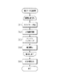
(補正データ生成処理)
次に、図2を用いて、補正データ生成処理について説明する。
ここでは、所定の階調毎に表示むらを抑制するための画像補正テーブルを生成する。具体的には、予め設定された階調(基準階調)毎に、液晶パネル10上の補正値の分布を算出する。本実施形態では、8bitで表現される信号値において所定数(例えば、10段階)の基準階調を用いることとし、基準階調に対応した調整対象階調を1段階毎に順次変更し、調整対象階調毎に画像補正テーブルを生成する。
(Correction data generation process)
Next, the correction data generation process will be described with reference to FIG.
Here, an image correction table for suppressing display unevenness is generated for each predetermined gradation. Specifically, the distribution of correction values on the
まず、画質調整装置20の制御部21は、テストパターン生成処理を実行する(ステップS1)。具体的には、制御部21のプロセス管理手段211は、テストパターン発生装置40に対して、調整対象階調の画像出力を行なうためのRGB信号の出力を指示する。ここでは、調整対象階調において、液晶パネル10全面に対して、R信号値、G信号値、B信号値が同じ信号(共通する信号値)を用いる。この指示に応じて、テストパターン発生装置40は、調整対象階調となる8bitのRGB信号を液晶パネル10に供給する。
First, the
そして、液晶パネル10は、これに応じて調整対象階調のグレー画像を出力する。この場合、液晶においてセルギャップのむらや、バックライトの明るさにむらがある場合には、液晶パネル10において、これらのむらが重畳された表示むらが生じる。ここで、撮影カメラ30は、表示むらが重畳された画像を撮影している。
In response to this, the
そして、画質調整装置20の制御部21は、出力画像の取得処理を実行する(ステップS2)。具体的には、制御部21のプロセス管理手段211は、液晶パネル10を撮影した出力画像データを撮影カメラ30から取り込む。そして、プロセス管理手段211は、この出力画像データを、8×8ピクセルから構成されたブロック毎の輝度分布に変換し、バンドパスフィルタ手段212に供給する。
And the
次に、画質調整装置20の制御部21は、バンドパスフィルタリング処理を実行する(ステップS3)。具体的には、制御部21のバンドパスフィルタ手段212は、取得した出力画像データに対してバンドパスフィルタリングを行なうことにより、バンドパスデータを算出する。このバンドパスデータは、液晶パネル10の面内の輝度分布に応じて、高周波成分及び低周波成分を除いた分布から構成される。そして、バンドパスフィルタ手段212は、生成したバンドパスデータをプロセス管理手段211に供給する。
Next, the
次に、画質調整装置20の制御部21は、補正値算出処理を実行する(ステップS4)。具体的には、制御部21のプロセス管理手段211は、バンドパスデータを反転させた画像補正テーブルを生成する。更に、プロセス管理手段211は、調整を行なった基準階調を特定する識別子に関連付けて画像補正テーブルをメモリに一時記憶する。
Next, the
そして、画質調整装置20の制御部21は、次の調整対象階調について、上述した処理を繰り返す。
すべての基準階調について補正データの算出を終了した場合、画質調整装置20の制御部21は、ROM書込処理を実行する(ステップS5)。具体的には、制御部21のプロセス管理手段211は、一時記憶した画像補正テーブルをROM51に書き込む。これにより、ROM51には、基準階調毎に、液晶パネル10の面内のブロック位置(xy座標)に対して補正値の分布が記録される。
And the
When the calculation of the correction data for all the reference gradations is completed, the
(画像表示処理)
そして、この液晶パネル10に対応して生成されたROM51は、補正回路50に組み込まれる。この補正回路は、液晶パネル10に供給される画像信号を調整するための回路である。具体的には、液晶パネル10に画像を表示するための画像信号(RGB信号)は、液晶パネル10とともに補正回路50にも供給される。
(Image display processing)
The
この補正回路50は、図3に示すように、ROM51の他に、選択・補間手段52、加算手段53を備える。
選択・補間手段52は、ROM51に記録された画像補正テーブルを、RGB信号毎に参照する。ここでは、選択・補間手段52は、画像信号の各RGB信号値に隣接する二つの基準階調の画像補正テーブルにおいて、画像信号のピクセル位置(xy座標)を囲む四つのブロック格子点によって決まる補正値(2×4=8個)を取得する。そして、選択・補間手段52は、取得した補正値について、画像信号の信号値と各格子点との距離に応じて線形補間を行なう。
As shown in FIG. 3, the
The selection / interpolation means 52 refers to the image correction table recorded in the
そして、加算手段53は、選択・補間手段52から取得した補正値を、入力された画像信号に加算する。液晶パネル10は、この補正された画像信号を取得して、画像を表示する。
Then, the adding
本実施形態によれば、以下のような効果を得ることができる。
・ 本実施形態では、補正回路50は、ROM51、選択・補間手段52、加算手段53を備える。このROM51には、撮影カメラ30によって撮影された画像における表示むらから生成された画像補正テーブルが記録される。表示むらは、各ピクセルの明るさが理想値と異なるために発生するので、予め各ピクセルの理想値とのズレを測定しておけば
、そのズレに従って各ピクセルへの入力画像値を補正することで表示むらをキャンセルすることが可能である。
According to this embodiment, the following effects can be obtained.
In the present embodiment, the
・ 本実施形態では、ROM51には、基準階調毎に画像補正テーブルが記録される。表示むらの発生は、同一ピクセルであっても入力レベルに対して一定していない。例えば、20%グレーを入力したときに19%のグレーが表示されるピクセルが、50%グレーにおいては51%グレーが、80%グレーでは83%グレーが表示されるというように変化することがある。ROM51には、基準階調毎に画像補正テーブルが記録されているために、各ピクセルの信号値に応じた補正を行なうことができる。
In the present embodiment, an image correction table is recorded in the
・ 本実施形態では、バンドパスフィルタリングを行なった分布を用いて画像補正テーブルを生成する。これにより、緩やかな輝度の変化については補正が行なわれない。液晶自体のむらが1%以下、多い場合にも5%程度に対して、バックライトの周辺減光は多いときは30%程度もあることがある。仮に低周波数成分の除去(ローカット)を行なわないで補正した場合、完全な白(100%グレー)画像に対して、液晶パネル10における周辺減光の影響を受けて、中心部付近の輝度を低下させてしまうことになる。
In this embodiment, an image correction table is generated using a distribution obtained by performing bandpass filtering. Thereby, correction is not performed for a gradual change in luminance. The unevenness of the liquid crystal itself may be about 1% or less, and about 5% even when there are many, whereas the backlight peripheral dimming may be about 30% when there are many. If correction is performed without removing low frequency components (low cut), the luminance near the center is reduced due to the influence of the peripheral dimming on the
このような場合、画面全体のなだらかな光量変化は人間の眼には検知され難く、ローカットを行なわない補正により液晶パネル10の輝度が落ちたことのみが目に付くことになる。
In such a case, a gentle change in the amount of light on the entire screen is difficult to be detected by the human eye, and only a drop in the brightness of the
また、非常に細かいむら(空間周波数の高い成分)も人間の眼に検知され難い。更に、非常に細かい表示むら(高周波数成分)を補正するには、正確に測定画像と液晶のピクセル位置の相関を取る必要があり、僅かでもずれるとかえって表示むらを作りこむことになる。従って、高周波数成分の除去(ハイカット)を行なうことにより、簡易かつ効率的に画像補正テーブルを生成することができる。 In addition, very fine unevenness (a component having a high spatial frequency) is hardly detected by human eyes. Further, in order to correct very fine display unevenness (high frequency component), it is necessary to accurately correlate the measurement image and the pixel position of the liquid crystal. If even a slight deviation occurs, display unevenness is created. Therefore, an image correction table can be generated easily and efficiently by removing high frequency components (high cut).
また、上記実施形態は以下のように変更してもよい。
○ 上記実施形態においては、モノクロカメラを用いて、輝度むらの補正を行なう。抑制対象の表示むらは輝度に限定されるものではなく、色むらの補正にも適用することが可能である。輝度むら及び色むら両方補正する場合は、RGB3つの光学フィルタを使って、それぞれ撮像手段で出力画像を取得する。そして、それぞれの画像から上記バンドパスフィルタリング処理(ステップS3)、補正値算出処理(ステップS4)により補正値を算出する。そして、R信号用、G信号用、B信号用の3種類の画像補正テーブルを作成し、ROM51に記録する。これにより、入力画像のRGBデータ値を補正して、色むらを抑制することができる。
Moreover, you may change the said embodiment as follows.
In the above embodiment, the luminance unevenness is corrected using a monochrome camera. The display unevenness to be suppressed is not limited to luminance, and can be applied to correction of color unevenness. When correcting both luminance unevenness and color unevenness, output images are acquired by the imaging means using RGB three optical filters. Then, a correction value is calculated from each image by the bandpass filtering process (step S3) and the correction value calculation process (step S4). Then, three types of image correction tables for R signal, G signal, and B signal are created and recorded in the
○ 上記実施形態においては、RGBの各信号値を一致させた画像を評価して、輝度むらの補正を行なう。色むらを補正する場合には、光学フィルタを用いるのではなく、単一色のR信号、G信号、B信号をそれぞれ独立して液晶パネル10に供給して、出力画像の取得処理(ステップS2)、バンドパスフィルタリング処理(ステップS3)、補正値算出処理(ステップS4)により画像補正テーブルを生成することも可能である。
In the above embodiment, the luminance nonuniformity is corrected by evaluating an image in which RGB signal values are matched. When correcting the color unevenness, an optical filter is not used, but a single color R signal, G signal, and B signal are independently supplied to the
○ 上記実施形態においては、液晶パネル10の表示むらの抑制に適用したが、調整対象の表示パネルはこれに限定されるものではない。プラズマディスプレィ(PDP)、投影型プロジェクタ等のような画像出力装置に適用することも可能である。
In the above embodiment, the present invention is applied to suppress the display unevenness of the
○ 上記実施形態においては、調整対象の液晶パネル10毎に、テストパターン生成処理(ステップS1)〜ROM書込処理(ステップS5)を実行する。これに代えて、調整対象の代表的な表示パネルにおいて、テストパターン生成処理(ステップS1)〜補正値
算出処理(ステップS4)を実行することにより、代表的な補正値を算出するようにしてもよい。そして、この代表的な補正値を書き込んだROMを作製し、補正回路50に組み込む。
In the above embodiment, the test pattern generation process (step S1) to the ROM writing process (step S5) are executed for each
例えば、代表的な液晶パネルにおける光源(バックライト)についての輝度むら(表示むら)の補正を行なう場合に適用することができる。液晶パネルにおいて、バックライトの灯数を減らしたり、拡散シートを除いたり、拡散板とランプとの距離を短くしたりした場合には、バックライトによる輝度むらが発生する。このようにバックライトによる輝度むらが発生した液晶パネルに対して、本願発明の画像補正を行なうことにより、表示むらを抑制することができる。この結果、ランプの灯数を削減する等、表示パネルを構成する部品点数を減らすことにより、コストダウンを図るとともに、高品質な表示パネルを製造することができる。又、ランプの灯数を削減した場合、バックライトの光量が減少するが、光学シート等を除いたり、ランプと拡散板との距離を近づけたりすることにより、光量を調整しながら均一な輝度を維持することができる。 For example, the present invention can be applied when correcting luminance unevenness (display unevenness) for a light source (backlight) in a typical liquid crystal panel. In the liquid crystal panel, when the number of backlights is reduced, the diffusion sheet is removed, or the distance between the diffusion plate and the lamp is shortened, uneven brightness due to the backlight occurs. By performing the image correction of the present invention on the liquid crystal panel in which the luminance unevenness due to the backlight occurs in this way, the display unevenness can be suppressed. As a result, by reducing the number of parts constituting the display panel, such as by reducing the number of lamps, the cost can be reduced and a high-quality display panel can be manufactured. In addition, when the number of lamps is reduced, the amount of light from the backlight decreases. However, by removing the optical sheet, etc., or by reducing the distance between the lamp and the diffuser, uniform brightness can be achieved while adjusting the amount of light. Can be maintained.
更に、このような代表的な補正値に対して、パネル毎に個別に本発明の画像補正を適用することも可能である。そして、各補正値についてROM書込処理を実行する。この場合には、個々の表示パネルの特性に基づく表示むらを抑制することができ、より高品質な表示パネルを製造することができる。すなわち、大まかな補正は代表的な画像補正により行ない、更に表示パネル毎に微調整することにより、効率的に画像補正を行なうことができる。 Furthermore, it is also possible to apply the image correction of the present invention individually for each panel to such a representative correction value. Then, ROM writing processing is executed for each correction value. In this case, display unevenness based on the characteristics of the individual display panels can be suppressed, and a higher quality display panel can be manufactured. That is, rough correction is performed by typical image correction, and further fine adjustment is performed for each display panel, whereby image correction can be performed efficiently.
10…液晶パネル、20…画質調整装置、21…制御部、211…プロセス管理手段、212…バンドパスフィルタ手段、30…撮影カメラ、40…テストパターン発生装置、50…補正回路、51…ROM。
DESCRIPTION OF
Claims (5)
前記表示パネルにおいて表示された出力画像を撮影する撮像手段と、
前記信号発生手段及び前記撮像手段に接続される制御手段と、を備えた画像補正データ生成システムであって、
前記制御手段が、
前記信号発生手段に対して、表示パネルの全面に共通する信号値の供給指示を出力する指示手段と、
前記撮像手段から、出力画像データを取得する画像取得手段と、
前記出力画像データに対し中間的な周波数成分のみを分離するバンドパスフィルタリングを行なうことによって、同出力画像データから高周波成分及び低周波成分を除いたバンドパスデータを算出するバンドパスフィルタ手段と、
前記バンドパスデータに対応した画像補正テーブルを出力する補正データ生成手段と
を備えたことを特徴とする画像補正データ生成システム。 Signal generating means for supplying a signal for outputting an image to the display panel;
Imaging means for capturing an output image displayed on the display panel;
An image correction data generation system comprising: the signal generation unit and a control unit connected to the imaging unit;
The control means is
Instruction means for outputting a signal value supply instruction common to the entire surface of the display panel to the signal generating means;
Image acquisition means for acquiring output image data from the imaging means;
Bandpass filter means for calculating bandpass data obtained by removing high frequency components and low frequency components from the output image data by performing bandpass filtering for separating only intermediate frequency components for the output image data;
An image correction data generation system comprising correction data generation means for outputting an image correction table corresponding to the bandpass data.
前記画像取得手段は、階調毎に出力画像データを取得し、
前記補正データ生成手段は、階調毎に画像補正テーブルを出力することを特徴とする請求項1に記載の画像補正データ生成システム。 The instruction means outputs a signal value supply instruction common to the entire surface of the display panel for each gradation,
The image acquisition means acquires output image data for each gradation,
The image correction data generation system according to claim 1, wherein the correction data generation unit outputs an image correction table for each gradation.
前記表示パネルにおいて表示された出力画像を撮影する撮像手段と、
前記信号発生手段及び前記撮像手段に接続される制御手段と、を備えた画像補正データ生成システムを用いて、画像補正データを生成する方法であって、
前記制御手段が、
前記信号発生手段に対して、表示パネルの全面に共通する信号値の供給指示を出力する指示段階と、
前記撮像手段から、出力画像データを取得する画像取得段階と、
前記出力画像データに対し中間的な周波数成分のみを分離するバンドパスフィルタリングを行なうことによって同出力画像データから高周波成分及び低周波成分を除いたバンドパスデータを算出するバンドパスフィルタリング段階と、
前記バンドパスデータに対応した画像補正テーブルを出力する補正データ生成段階と
を実行することを特徴とする画像補正データ生成方法。 Signal generating means for supplying a signal for outputting an image to the display panel;
Imaging means for capturing an output image displayed on the display panel;
A method of generating image correction data using an image correction data generation system comprising: the signal generation means and a control means connected to the imaging means;
The control means is
An instruction step of outputting a signal value supply instruction common to the entire surface of the display panel to the signal generating means;
An image acquisition step of acquiring output image data from the imaging means;
A bandpass filtering step of calculating bandpass data obtained by removing high frequency components and low frequency components from the output image data by performing bandpass filtering for separating only intermediate frequency components for the output image data;
And a correction data generation step of outputting an image correction table corresponding to the bandpass data.
前記画像補正テーブルはバンドパスデータに対応して生成されており、このバンドパスデータは、前記表示パネルの全面に供給された共通する信号値に基づいて前記表示パネルに表示された出力画像を撮像して得た出力画像データに対して中間的な周波数成分のみを分離するバンドパスフィルタリングを行なって、同出力画像データから高周波成分及び低周波成分を除くことによって得られ、
前記表示パネルに供給される画像信号に対して、前記画像補正テーブルに基づいて、出力画像を補正する信号を出力することにより、前記表示パネルの出力画像を調整するための画像補正回路。 An image correction circuit storing an image correction table for adjusting an image signal supplied to a display panel,
The image correction table is generated corresponding to bandpass data, and the bandpass data captures an output image displayed on the display panel based on a common signal value supplied to the entire surface of the display panel. It is obtained by performing band-pass filtering that separates only intermediate frequency components from the output image data obtained by removing high frequency components and low frequency components from the output image data,
An image correction circuit for adjusting an output image of the display panel by outputting a signal for correcting an output image based on the image correction table with respect to an image signal supplied to the display panel.
Priority Applications (7)
| Application Number | Priority Date | Filing Date | Title |
|---|---|---|---|
| JP2008227139A JP4681033B2 (en) | 2008-07-31 | 2008-09-04 | Image correction data generation system, image data generation method, and image correction circuit |
| PCT/JP2009/063511 WO2010013753A1 (en) | 2008-07-31 | 2009-07-29 | Image correction data generation system, image correction data generation method, image correction data generation program, and image correction circuit |
| CN200980119693.3A CN102150197B (en) | 2008-07-31 | 2009-07-29 | Image correction data generation system, image correction data generation method, image correction data generation program, and image correction circuit |
| KR1020107025226A KR101165026B1 (en) | 2008-07-31 | 2009-07-29 | Image correction data generation system, image correction data generation method, image correction data generation program, and image correction circuit |
| CN201410370128.7A CN104217666B (en) | 2008-07-31 | 2009-07-29 | Image quality adjustment device, image correction circuit and display panel |
| TW098125754A TWI485695B (en) | 2008-07-31 | 2009-07-30 | Image correction data generating system, image correction data generating method, image correction data generating program and image correction circuit |
| TW101119774A TWI520126B (en) | 2008-07-31 | 2009-07-30 | Image correction data generating system, image correction data generating method, image correction data generating program and image correction circuit |
Applications Claiming Priority (2)
| Application Number | Priority Date | Filing Date | Title |
|---|---|---|---|
| JP2008197876 | 2008-07-31 | ||
| JP2008227139A JP4681033B2 (en) | 2008-07-31 | 2008-09-04 | Image correction data generation system, image data generation method, and image correction circuit |
Related Child Applications (1)
| Application Number | Title | Priority Date | Filing Date |
|---|---|---|---|
| JP2011021056A Division JP5362753B2 (en) | 2008-07-31 | 2011-02-02 | Image quality adjustment apparatus and image correction data generation program |
Publications (3)
| Publication Number | Publication Date |
|---|---|
| JP2010057149A JP2010057149A (en) | 2010-03-11 |
| JP2010057149A5 JP2010057149A5 (en) | 2010-11-11 |
| JP4681033B2 true JP4681033B2 (en) | 2011-05-11 |
Family
ID=41610452
Family Applications (1)
| Application Number | Title | Priority Date | Filing Date |
|---|---|---|---|
| JP2008227139A Active JP4681033B2 (en) | 2008-07-31 | 2008-09-04 | Image correction data generation system, image data generation method, and image correction circuit |
Country Status (5)
| Country | Link |
|---|---|
| JP (1) | JP4681033B2 (en) |
| KR (1) | KR101165026B1 (en) |
| CN (2) | CN102150197B (en) |
| TW (2) | TWI520126B (en) |
| WO (1) | WO2010013753A1 (en) |
Cited By (1)
| Publication number | Priority date | Publication date | Assignee | Title |
|---|---|---|---|---|
| JP2013250570A (en) * | 2008-07-31 | 2013-12-12 | Iix Inc | Image quality adjusting device and image correction data generation program |
Families Citing this family (25)
| Publication number | Priority date | Publication date | Assignee | Title |
|---|---|---|---|---|
| JP4777472B1 (en) * | 2010-08-24 | 2011-09-21 | 株式会社イクス | Image correction data generation system, display correction data generation method, and image correction data generation program for display panel using non-polished glass |
| JP2012053579A (en) * | 2010-08-31 | 2012-03-15 | Iix Inc | Production management system and production management method |
| JP5113232B2 (en) * | 2010-09-08 | 2013-01-09 | 株式会社イクス | Panel evaluation system and panel evaluation method |
| JP2012085225A (en) * | 2010-10-14 | 2012-04-26 | Iix Inc | Image quality adjustment system and image quality adjustment method |
| KR101784216B1 (en) | 2011-02-14 | 2017-10-12 | 삼성디스플레이 주식회사 | Compensation table generating system, display apparatus having brightness compensating table and method of generating compensation table |
| JP2012048206A (en) * | 2011-06-27 | 2012-03-08 | Iix Inc | Image correction data generation system for display panel using unpolished glass, image correction data generation method, and image correction data generation program |
| JPWO2013038560A1 (en) * | 2011-09-16 | 2015-03-23 | Necディスプレイソリューションズ株式会社 | Display device and method for correcting unevenness of display device |
| JP5919370B2 (en) | 2012-03-01 | 2016-05-18 | 株式会社日本マイクロニクス | Method and apparatus for detecting display unevenness of display device |
| KR101640118B1 (en) | 2012-03-01 | 2016-07-15 | 가부시키가이샤 니혼 마이크로닉스 | Display unevenness detection method and device for display device |
| JP2012186825A (en) * | 2012-04-24 | 2012-09-27 | Iix Inc | Image quality adjustment device, image quality adjustment system, and image quality adjustment method |
| WO2014050222A1 (en) * | 2012-09-25 | 2014-04-03 | 株式会社イクス | Image quality adjustment device, correction data generation method, and image quality adjustment technique utilizing same |
| JP5634473B2 (en) * | 2012-10-11 | 2014-12-03 | 株式会社イクス | Panel evaluation system and panel evaluation method |
| JP2014086996A (en) | 2012-10-26 | 2014-05-12 | Iix Inc | Picture quality adjustment device, picture quality adjustment circuit (ic), and display panel |
| JPWO2014128822A1 (en) * | 2013-02-19 | 2017-02-02 | 株式会社イクス | Correction data generation method, correction data generation system, and image quality adjustment technique using them |
| WO2014128821A1 (en) | 2013-02-19 | 2014-08-28 | 株式会社イクス | Pattern position detection method, pattern position detection system, and image quality adjustment technique using pattern position detection method and pattern position detection system |
| CN105051506B (en) * | 2013-04-08 | 2017-06-23 | 宜客斯股份有限公司 | Brightness measurement method, brightness measuring device for camera and use their image quality adjustment technology |
| JP6243030B2 (en) * | 2014-07-15 | 2017-12-06 | 株式会社イクス | Image processing method and image processing apparatus for executing the image processing method |
| JP6588700B2 (en) | 2014-12-09 | 2019-10-09 | 株式会社メガチップス | Correction data generation method, image correction apparatus, image correction method, and image correction system |
| WO2016149877A1 (en) | 2015-03-20 | 2016-09-29 | 华为技术有限公司 | Method for correcting screen asymmetry and device and system thereof |
| CN106612355B (en) * | 2015-10-23 | 2020-03-06 | 宁波舜宇光电信息有限公司 | Production method and system for single correction production line of mobile phone camera module |
| WO2017187827A1 (en) * | 2016-04-28 | 2017-11-02 | 株式会社イクス | Irregularity evaluating method and irregularity evaluating device |
| WO2018146765A1 (en) | 2017-02-09 | 2018-08-16 | 株式会社イクス | Image processing method and image processing device for executing image processing method |
| CN107957796A (en) * | 2017-12-01 | 2018-04-24 | 民办四川天学院 | Measure the drawing boards and its measuring method of distance between drawing boards and drawing pen |
| WO2020136732A1 (en) | 2018-12-25 | 2020-07-02 | 堺ディスプレイプロダクト株式会社 | Correction image generation system, image control method, image control program, and recording medium |
| TWI819411B (en) * | 2021-11-23 | 2023-10-21 | 瑞昱半導體股份有限公司 | Image processing apparatus and image processing method for contrast enhancement |
Citations (3)
| Publication number | Priority date | Publication date | Assignee | Title |
|---|---|---|---|---|
| JP2001324960A (en) * | 2000-03-10 | 2001-11-22 | Ngk Insulators Ltd | Display system and display management method |
| WO2003071794A1 (en) * | 2002-02-19 | 2003-08-28 | Olympus Corporation | Image correction data calculation method, image correction data calculation device, and projection system |
| JP2007086581A (en) * | 2005-09-26 | 2007-04-05 | Seiko Epson Corp | Image processing apparatus, electrooptical device, electronic equipment, and data generating method |
Family Cites Families (8)
| Publication number | Priority date | Publication date | Assignee | Title |
|---|---|---|---|---|
| JP3672586B2 (en) * | 1994-03-24 | 2005-07-20 | 株式会社半導体エネルギー研究所 | Correction system and operation method thereof |
| JPH1141629A (en) * | 1997-07-15 | 1999-02-12 | Minolta Co Ltd | Calibration pattern display device and display characteristics measuring device for a color display device applied with the calibration pattern display device |
| JP2000181407A (en) * | 1998-12-10 | 2000-06-30 | Fujitsu Ltd | Liquid crystal display device |
| TWI220689B (en) * | 2002-12-27 | 2004-09-01 | Ind Tech Res Inst | An inspection system and method for the inspection of a display device |
| TWM244536U (en) * | 2003-08-21 | 2004-09-21 | Etoms Electronics Corp | 2D detection and displacement judging architecture having neural network |
| JP2006074155A (en) * | 2004-08-31 | 2006-03-16 | Mitsubishi Electric Corp | Device and method for image processing, and image display device |
| TWI273232B (en) * | 2004-09-27 | 2007-02-11 | Kubotek Corp | Optical inspection system and method thereof for operating a plurality of defect inspection operations to a substrate |
| JP4438696B2 (en) * | 2005-06-15 | 2010-03-24 | セイコーエプソン株式会社 | Image display apparatus and method |
-
2008
- 2008-09-04 JP JP2008227139A patent/JP4681033B2/en active Active
-
2009
- 2009-07-29 CN CN200980119693.3A patent/CN102150197B/en active Active
- 2009-07-29 CN CN201410370128.7A patent/CN104217666B/en active Active
- 2009-07-29 KR KR1020107025226A patent/KR101165026B1/en active IP Right Review Request
- 2009-07-29 WO PCT/JP2009/063511 patent/WO2010013753A1/en active Application Filing
- 2009-07-30 TW TW101119774A patent/TWI520126B/en active
- 2009-07-30 TW TW098125754A patent/TWI485695B/en active
Patent Citations (3)
| Publication number | Priority date | Publication date | Assignee | Title |
|---|---|---|---|---|
| JP2001324960A (en) * | 2000-03-10 | 2001-11-22 | Ngk Insulators Ltd | Display system and display management method |
| WO2003071794A1 (en) * | 2002-02-19 | 2003-08-28 | Olympus Corporation | Image correction data calculation method, image correction data calculation device, and projection system |
| JP2007086581A (en) * | 2005-09-26 | 2007-04-05 | Seiko Epson Corp | Image processing apparatus, electrooptical device, electronic equipment, and data generating method |
Cited By (1)
| Publication number | Priority date | Publication date | Assignee | Title |
|---|---|---|---|---|
| JP2013250570A (en) * | 2008-07-31 | 2013-12-12 | Iix Inc | Image quality adjusting device and image correction data generation program |
Also Published As
| Publication number | Publication date |
|---|---|
| CN104217666B (en) | 2017-01-11 |
| KR101165026B1 (en) | 2012-07-13 |
| KR20110002474A (en) | 2011-01-07 |
| CN102150197A (en) | 2011-08-10 |
| WO2010013753A1 (en) | 2010-02-04 |
| TW201239870A (en) | 2012-10-01 |
| CN104217666A (en) | 2014-12-17 |
| TW201011731A (en) | 2010-03-16 |
| JP2010057149A (en) | 2010-03-11 |
| CN102150197B (en) | 2014-08-20 |
| TWI520126B (en) | 2016-02-01 |
| TWI485695B (en) | 2015-05-21 |
Similar Documents
| Publication | Publication Date | Title |
|---|---|---|
| JP4681033B2 (en) | Image correction data generation system, image data generation method, and image correction circuit | |
| JP4109702B1 (en) | Image quality adjustment apparatus, image quality adjustment method, and image quality adjustment program | |
| US8610781B2 (en) | System and method for light compensation in a video panel display | |
| CN108234975A (en) | Combination color homogeneity and consistency control method based on video camera | |
| WO2014128821A1 (en) | Pattern position detection method, pattern position detection system, and image quality adjustment technique using pattern position detection method and pattern position detection system | |
| CN104505021B (en) | pixel display adjusting method and device | |
| US9508281B2 (en) | Apparatus and method for image analysis and image display | |
| JPWO2011013404A1 (en) | Image display device and image display method | |
| JPWO2014128822A1 (en) | Correction data generation method, correction data generation system, and image quality adjustment technique using them | |
| KR101444043B1 (en) | Image correction data generating system and image correction data generating method for display panel using unpolished glass | |
| JP2009128733A (en) | Liquid crystal display, control circuit, liquid crystal display control method, and computer program | |
| WO2005064584A1 (en) | Display system | |
| JP5362753B2 (en) | Image quality adjustment apparatus and image correction data generation program | |
| JP2013044959A (en) | Image display device and control method thereof | |
| JP2008158117A (en) | Image processor | |
| JP6548516B2 (en) | IMAGE DISPLAY DEVICE, IMAGE PROCESSING DEVICE, CONTROL METHOD OF IMAGE DISPLAY DEVICE, AND CONTROL METHOD OF IMAGE PROCESSING DEVICE | |
| JPH06105185A (en) | Brightness correction method | |
| JP2012048206A (en) | Image correction data generation system for display panel using unpolished glass, image correction data generation method, and image correction data generation program | |
| JP2021081494A (en) | Image processing system, image processing method, and image processing program | |
| JP2012063440A (en) | Display device | |
| TW202403712A (en) | Information processing system, adjustment method, and program | |
| JP2021157070A (en) | Image display device and image display device control method | |
| CN116848574A (en) | Uneven correction data generation device | |
| CN117524143A (en) | Compensation method and system of display panel, display device and storage medium | |
| JP2020068414A (en) | Video display system and method of correcting color unevenness of video display device |
Legal Events
| Date | Code | Title | Description |
|---|---|---|---|
| A521 | Request for written amendment filed |
Free format text: JAPANESE INTERMEDIATE CODE: A523 Effective date: 20100924 |
|
| A621 | Written request for application examination |
Free format text: JAPANESE INTERMEDIATE CODE: A621 Effective date: 20100924 |
|
| A871 | Explanation of circumstances concerning accelerated examination |
Free format text: JAPANESE INTERMEDIATE CODE: A871 Effective date: 20100924 |
|
| A975 | Report on accelerated examination |
Free format text: JAPANESE INTERMEDIATE CODE: A971005 Effective date: 20101013 |
|
| A131 | Notification of reasons for refusal |
Free format text: JAPANESE INTERMEDIATE CODE: A131 Effective date: 20101026 |
|
| A521 | Request for written amendment filed |
Free format text: JAPANESE INTERMEDIATE CODE: A523 Effective date: 20101206 |
|
| TRDD | Decision of grant or rejection written | ||
| A01 | Written decision to grant a patent or to grant a registration (utility model) |
Free format text: JAPANESE INTERMEDIATE CODE: A01 Effective date: 20110104 |
|
| A01 | Written decision to grant a patent or to grant a registration (utility model) |
Free format text: JAPANESE INTERMEDIATE CODE: A01 |
|
| A61 | First payment of annual fees (during grant procedure) |
Free format text: JAPANESE INTERMEDIATE CODE: A61 Effective date: 20110203 |
|
| R150 | Certificate of patent or registration of utility model |
Ref document number: 4681033 Country of ref document: JP Free format text: JAPANESE INTERMEDIATE CODE: R150 Free format text: JAPANESE INTERMEDIATE CODE: R150 |
|
| FPAY | Renewal fee payment (event date is renewal date of database) |
Free format text: PAYMENT UNTIL: 20140210 Year of fee payment: 3 |
|
| FPAY | Renewal fee payment (event date is renewal date of database) |
Free format text: PAYMENT UNTIL: 20140210 Year of fee payment: 3 |
|
| RD02 | Notification of acceptance of power of attorney |
Free format text: JAPANESE INTERMEDIATE CODE: R3D02 |
|
| R250 | Receipt of annual fees |
Free format text: JAPANESE INTERMEDIATE CODE: R250 |
|
| R250 | Receipt of annual fees |
Free format text: JAPANESE INTERMEDIATE CODE: R250 |
|
| R250 | Receipt of annual fees |
Free format text: JAPANESE INTERMEDIATE CODE: R250 |
|
| R250 | Receipt of annual fees |
Free format text: JAPANESE INTERMEDIATE CODE: R250 |
|
| R250 | Receipt of annual fees |
Free format text: JAPANESE INTERMEDIATE CODE: R250 |
|
| R250 | Receipt of annual fees |
Free format text: JAPANESE INTERMEDIATE CODE: R250 |
|
| R250 | Receipt of annual fees |
Free format text: JAPANESE INTERMEDIATE CODE: R250 |
|
| R250 | Receipt of annual fees |
Free format text: JAPANESE INTERMEDIATE CODE: R250 |
|
| R250 | Receipt of annual fees |
Free format text: JAPANESE INTERMEDIATE CODE: R250 |
|
| R250 | Receipt of annual fees |
Free format text: JAPANESE INTERMEDIATE CODE: R250 |
|
| R250 | Receipt of annual fees |
Free format text: JAPANESE INTERMEDIATE CODE: R250 |