JP4678676B2 - Method or apparatus for measuring physical or chemical phenomena - Google Patents
Method or apparatus for measuring physical or chemical phenomena Download PDFInfo
- Publication number
- JP4678676B2 JP4678676B2 JP2005225505A JP2005225505A JP4678676B2 JP 4678676 B2 JP4678676 B2 JP 4678676B2 JP 2005225505 A JP2005225505 A JP 2005225505A JP 2005225505 A JP2005225505 A JP 2005225505A JP 4678676 B2 JP4678676 B2 JP 4678676B2
- Authority
- JP
- Japan
- Prior art keywords
- charge
- unit
- sensing
- physical
- chemical
- Prior art date
- Legal status (The legal status is an assumption and is not a legal conclusion. Google has not performed a legal analysis and makes no representation as to the accuracy of the status listed.)
- Expired - Fee Related
Links
Images


Classifications
-
- G—PHYSICS
- G01—MEASURING; TESTING
- G01N—INVESTIGATING OR ANALYSING MATERIALS BY DETERMINING THEIR CHEMICAL OR PHYSICAL PROPERTIES
- G01N27/00—Investigating or analysing materials by the use of electric, electrochemical, or magnetic means
- G01N27/26—Investigating or analysing materials by the use of electric, electrochemical, or magnetic means by investigating electrochemical variables; by using electrolysis or electrophoresis
- G01N27/403—Cells and electrode assemblies
- G01N27/414—Ion-sensitive or chemical field-effect transistors, i.e. ISFETS or CHEMFETS
- G01N27/4148—Integrated circuits therefor, e.g. fabricated by CMOS processing
Description
本発明は、物理現象または化学現象を定量化する測定方法および装置に関し、例えば、溶液のpH、圧力、磁界、あるいは温度の二次元分布など、様々の物理現象または化学現象を定量化する測定方法および装置に関する。 The present invention relates to a measurement method and apparatus for quantifying a physical phenomenon or chemical phenomenon, and for example, a measurement method for quantifying various physical or chemical phenomena such as a two-dimensional distribution of pH, pressure, magnetic field, or temperature of a solution. And apparatus.
物理現象または化学現象には、濃度、温度、磁気、圧力、加速度、速度、音波、超音波、酸化還元電位、反応速度など様々な現象があるが、これらの現象は、様々な電気信号(電流、電圧、抵抗、電荷容量、電位)に変換することができる。 Physical or chemical phenomena include various phenomena such as concentration, temperature, magnetism, pressure, acceleration, velocity, sound wave, ultrasonic wave, redox potential, reaction rate, etc. These phenomena are various electric signals (currents). , Voltage, resistance, charge capacity, potential).
また、例えば、フォトダイオードのように、光を照射すると光量に応じた電子正孔対が生成し、光量を電荷量に変化してその電荷量を評価することにより光量を測定する方法などのように、物理現象または化学現象を電荷情報に変換して測定する方法があった。 Also, for example, a method of measuring the light quantity by changing the light quantity into a charge quantity and evaluating the charge quantity, such as a photodiode, when light is irradiated, generates an electron-hole pair according to the quantity of light. In addition, there is a method for measuring physical phenomena or chemical phenomena by converting them into charge information.
しかしながら、光以外のその他の物理・化学現象においては、ほとんどの場合、電荷量ではなく、電圧値、電流値、抵抗値などの電気信号に変換し、それらの値を読み取るようにしているため、電荷特有の取扱い方法である蓄積および転送を行うことができず、また複数点の情報を同時に取り込んで高速処理したり、測定結果を画像化するといったことが非常に困難であった。 However, in other physical and chemical phenomena other than light, in most cases, instead of the amount of charge, it is converted into an electrical signal such as a voltage value, current value, resistance value, etc., so that those values are read. Accumulation and transfer, which are peculiar to electric charges, cannot be performed, and it is very difficult to simultaneously acquire information from a plurality of points and perform high-speed processing or to image measurement results.
近年、環境あるいは医療の分野を含め各種の分野において、こうした物理現象または化学現象の高速処理化あるいは画像化の要請が高まり、例えば、物理的または化学的な量の大きさに対応して深さを変化するように構成されたポテンシャル井戸に電荷を供給して、前記物理的または化学的な量をこのポテンシャル井戸の大きさに応じた電荷に変換することによって、複数点の情報を同時に取り込み、蓄積、転送などを行い、様々な物理現象または化学現象を容易に画像化できるようにした方法および装置などが提案されている(例えば特許文献1参照)。
しかしながら、昨今の物理現象または化学現象の測定には、従来以上に精緻な測定精度や応答の高速化が求められ、上記の方法や装置に対し、より優れた精度面あるいは応答面の改善の要請が強くなってきた。 However, the recent measurement of physical or chemical phenomena requires more precise measurement accuracy and faster response than before, and there is a need for better accuracy and response improvements to the above methods and devices. Has become stronger.
つまり、物理現象または化学現象を電荷情報として変換するに際し、精度面あるいは応答面に対しては、電荷の移動をより効率的にかつ迅速に行うために電荷移動手段をどのような構成あるいは構造とすることが好ましいかが大きな課題となってきた。 In other words, when converting physical phenomena or chemical phenomena as charge information, the charge transfer means has any configuration or structure in order to move charges more efficiently and quickly with respect to accuracy or response. Whether to do it has become a major issue.
また、物理現象または化学現象の測定においては、大きな変化による大量の電荷移動がある場合と物理現象または化学現象としての変化がほとんどなく小さな電荷移動しか発生しない場合がある。実際の測定においては、いずれの場合においても現象変化に対応した所定の測定精度を要求されるが、同一構成の検出器において、そのいずれの電荷移動条件においても同一精度を確保することは非常に難しい。つまり、検出器にとって広い範囲での直線性確保は大きな課題である。 In the measurement of a physical phenomenon or chemical phenomenon, there is a case where there is a large amount of charge transfer due to a large change and a case where there is almost no change as a physical phenomenon or chemical phenomenon and only a small charge transfer occurs. In actual measurement, a predetermined measurement accuracy corresponding to the phenomenon change is required in any case, but it is very difficult to ensure the same accuracy in any charge transfer condition in a detector having the same configuration. difficult. In other words, ensuring linearity in a wide range is a big problem for the detector.
そこで、この発明の目的は、物理現象または化学現象を電荷情報に変換することによって定量化を行い、高い測定精度および優れた応答性、さらに優れた直線性を有する測定方法あるいは測定装置を提供することにある。また、複数点の電荷情報を同時に取り込み様々な物理現象または化学現象を容易に画像化できる測定方法および測定装置を提供することを目的とする。 Accordingly, an object of the present invention is to provide a measuring method or measuring apparatus that performs quantification by converting physical or chemical phenomena into charge information, and has high measurement accuracy, excellent responsiveness, and excellent linearity. There is. It is another object of the present invention to provide a measurement method and a measurement apparatus that can simultaneously capture charge information at a plurality of points and easily image various physical or chemical phenomena.
本発明者らは、上記課題を解決するために、鋭意研究を重ねた結果、以下に示す測定方法あるいは測定装置によって上記目的を達成できることを見出し、本発明を完成するに到った。 As a result of intensive studies to solve the above problems, the present inventors have found that the above object can be achieved by the following measuring method or measuring apparatus, and have completed the present invention.
本発明は、物理的または化学的な量の大きさに対応して電位が変化するセンシング部に対して電荷供給部から電荷を供給し、供給された電荷をセンシング部からフローティングディフュージョンを介して取出し、供給された電荷量を検出することによって該物理現象または化学現象を測定する方法であって、
前記センシング部からの電荷をフローティングディフュージョンの前段で蓄積し、その一部を放出するとともに、物理的または化学的な量の大きさに対応する電位に相当する電荷を含む電荷量をフローティングディフュージョンに転送すること、および前記放出量を変更可能とすることを特徴とする。
The present invention supplies a charge from a charge supply unit to a sensing unit whose potential changes according to the magnitude of a physical or chemical quantity, and takes out the supplied charge from the sensing unit via a floating diffusion. A method of measuring the physical or chemical phenomenon by detecting the amount of charge supplied, comprising:
The charge from the sensing unit is accumulated in the front stage of the floating diffusion, and a part of the charge is discharged, and the charge amount including the charge corresponding to the potential corresponding to the magnitude of the physical or chemical amount is transferred to the floating diffusion. And the amount of discharge can be changed.
また、本発明は、物理的または化学的な量の大きさに対応して電位が変化するセンシング部を閾として電荷供給部から電荷を供給し、供給された電荷をセンシング部からフローティングディフュージョンを介して取出し、供給された電荷量を検出することによって該物理現象または化学現象を測定する方法であって、
前記センシング部からの電荷をフローティングディフュージョンの前段で蓄積し、その一部を放出するとともに、物理的または化学的な量の大きさに対応する電位に相当する電荷を含む電荷量をフローティングディフュージョンに転送すること、および前記放出量を変更可能とすることを特徴とする。
In addition, the present invention supplies charges from the charge supply unit with a sensing unit whose potential changes corresponding to the magnitude of a physical or chemical quantity as a threshold, and supplies the supplied charge from the sensing unit via a floating diffusion. A method of measuring the physical phenomenon or chemical phenomenon by detecting the amount of electric charge taken out and supplied,
The charge from the sensing unit is accumulated in the front stage of the floating diffusion, and a part of the charge is discharged, and the charge amount including the charge corresponding to the potential corresponding to the magnitude of the physical or chemical amount is transferred to the floating diffusion. And the amount of discharge can be changed.
さらに、本発明は、電荷をセンシング部に供給する電荷供給部、物理的または化学的な量の大きさに対応して電位が変化するセンシング部、該センシング部に供給された電荷を取出すフローティングディフュージョンからなる検出部を有する測定装置であって、
前記センシング部とフローティングディフュージョンの中間に、
該センシング部から転送された電荷を蓄積するセンシング電荷蓄積部、該センシング電荷蓄積部に蓄積された電荷の一部を放出するリセットゲート、
および残りの電荷をフローティングディフュージョンに転送する堰部を有することを特徴とする。
Furthermore, the present invention provides a charge supply unit that supplies charges to the sensing unit, a sensing unit that changes in potential according to the magnitude of a physical or chemical amount, and a floating diffusion that extracts the charge supplied to the sensing unit. A measuring device having a detection unit comprising:
Between the sensing unit and the floating diffusion,
A sensing charge accumulating unit for accumulating the charge transferred from the sensing unit, a reset gate for releasing a part of the electric charge accumulated in the sensing charge accumulating unit,
And a weir for transferring the remaining charge to the floating diffusion.
また、本発明は、電荷をセンシング部に供給する電荷供給部、物理的または化学的な量の大きさに対応して電位が変化するセンシング部、該センシング部を閾として供給された電荷を取出すフローティングディフュージョンからなる検出部を有する測定装置であって、
前記センシング部とフローティングディフュージョンの中間に、
該センシング部から転送された電荷を蓄積するセンシング電荷蓄積部、該センシング電荷蓄積部に蓄積された電荷の一部を放出するリセットゲート、
および残りの電荷をフローティングディフュージョンに転送する堰部を有することを特徴とする。
The present invention also provides a charge supply unit that supplies charge to the sensing unit, a sensing unit that changes in potential according to the magnitude of a physical or chemical amount, and a charge that is supplied using the sensing unit as a threshold. A measuring device having a detection unit made of a floating diffusion,
Between the sensing unit and the floating diffusion,
A sensing charge accumulating unit for accumulating the charge transferred from the sensing unit, a reset gate for releasing a part of the electric charge accumulated in the sensing charge accumulating unit,
And a weir for transferring the remaining charge to the floating diffusion.
物理的または化学的な量の大きさに対応して電位(以下「検出電位」という。)が変化するセンシング部を有し、電荷量を検出することによって該物理現象または化学現象を測定する方法は、現象を電荷信号に変換することによって、加除が容易で蓄積を行うことができることから、信号の平均化によるノイズを低減することができる。また、蓄積回数を増やすことによって、微小信号の検出が可能となり、検出精度の向上を図ることができる点において優れている。さらには、物理的または化学的な量の変化に対応した電荷量(以下「測定電荷量」という。)のみを検出することが好ましい。 A method of measuring a physical phenomenon or a chemical phenomenon by detecting a charge amount, having a sensing unit in which a potential (hereinafter referred to as “detection potential”) changes in accordance with the magnitude of a physical or chemical amount. By converting the phenomenon into a charge signal, addition and subtraction can be easily performed and accumulation can be performed, so that noise due to signal averaging can be reduced. Further, by increasing the number of times of accumulation, it is excellent in that a minute signal can be detected and detection accuracy can be improved. Furthermore, it is preferable to detect only a charge amount (hereinafter referred to as “measurement charge amount”) corresponding to a change in physical or chemical amount.
しかし、現実には、それに加え、測定に関係しない電荷(オフセット電荷)や、検出系の周辺あるいは電荷処理系からの影響、例えば、温度や磁場あるいは電場などの影響により発生する電荷(外乱)を検出することになる。特に、センシング部からの電荷あるいはセンシング部を閾として転送した電荷が転送されるフローティングディフュージョンには容量の限界があり、検出感度を上げるために増やす蓄積回数にも限界があった。 However, in reality, in addition to this, there are charges that are not related to measurement (offset charges), influences from the periphery of the detection system or from the charge processing system, such as charges (disturbances) generated by the influence of temperature, magnetic field, electric field, etc. Will be detected. In particular, the floating diffusion to which the charge from the sensing unit or the charge transferred with the sensing unit as a threshold is transferred has a capacity limit, and the number of accumulations to increase the detection sensitivity is also limited.
そこで、本発明は、こうした測定電荷量以外の電荷を排除すべく検討した結果、センシング部からの電荷あるいはセンシング部を閾として転送した電荷を蓄積し、その一部を放出した後にフローティングディフュージョンに転送することが、外乱影響を削減し、かつS/N比を向上させるのに有効であることを見出した。つまり、フローティングディフュージョンに転送される電荷中の測定電荷量以外の成分を少なくすることによって、従来よりもはるかに多くの蓄積が可能となりノイズが軽減されS/N比が向上される。従って、測定精度の向上と併せて、検出特性の直線性の改善を図ることができる。 Therefore, as a result of studying to eliminate charges other than the measured charge amount, the present invention accumulates the charge from the sensing part or the charge transferred with the sensing part as a threshold, and after releasing part of the charge, transfers it to the floating diffusion. Has been found to be effective in reducing the influence of disturbance and improving the S / N ratio. That is, by reducing the components other than the measured charge amount in the charge transferred to the floating diffusion, much more accumulation is possible than before, noise is reduced, and the S / N ratio is improved. Therefore, it is possible to improve the linearity of the detection characteristics together with the improvement of the measurement accuracy.
ここで、フローティングディフュージョンの前段に蓄積された電荷の放出量は、通常、予め確認された特性からリセットゲートによって一定量に設定することも可能であるが、後述するように、リセットゲートあるいは堰部によって調整ができるようにすることが有用である。 Here, the discharge amount of the charge accumulated in the previous stage of the floating diffusion can be normally set to a fixed amount by the reset gate from the characteristics confirmed in advance. It is useful to be able to make adjustments.
従って、物理現象または化学現象を電荷情報に変換することによって定量化を行い、高い測定精度および優れた応答性、さらに優れた直線性を有する測定方法あるいは測定装置を提供することが可能となった。 Therefore, it is possible to provide a measuring method or measuring apparatus that performs quantification by converting physical or chemical phenomena into charge information, and has high measurement accuracy, excellent responsiveness, and excellent linearity. .
本発明は、上記物理現象または化学現象の測定方法であって、物理的または化学的な量の大きさに対応して電位が変化するセンシング部を有する前記機能を有する検出系Aと、物理的または化学的な量の変化に感応しないセンシング部を有しセンシング部以外の機能を同じくする検出系Bからなる一対の検出系によって該物理現象または化学現象を測定する方法であって、検出系Aにおける前記放出量を、検出系Bにおいてフローティングディフュージョンの前段で蓄積された電荷量に連動して変更することを特徴とする。 The present invention is a method of measuring a physical phenomenon or a chemical phenomenon, and includes a detection system A having the above-described function having a sensing unit in which a potential changes in accordance with a physical or chemical quantity, Or a method of measuring the physical phenomenon or chemical phenomenon by a pair of detection systems comprising a detection system B having a sensing unit that is insensitive to a change in chemical quantity and having the same function as the sensing unit, the detection system A In the detection system B, the discharge amount is changed in conjunction with the charge amount accumulated in the previous stage of the floating diffusion.
また、本発明は、同一の構造の前記電荷供給部、センシング電荷蓄積部、およびリセットゲートを有する少なくとも一対の検出系を有する測定装置であって、
物理的または化学的な量の大きさに対応して電位が変化するセンシング部を有し、センシング部に供給された電荷の一部がセンシング電荷蓄積部および障壁部を介してフローティングディフュージョンに転送される検出系Aと、
物理的または化学的な量の変化に感応しないセンシング部を有し、センシング部以外の機能を検出系Aと同じくする検出系Bからなるとともに、
検出系Bのセンシング電荷蓄積部に蓄積された電荷量に連動して、検出系Aの障壁部から転送する電荷量を変化させることを特徴とする。
Further, the present invention is a measuring apparatus having at least a pair of detection systems having the charge supply unit, the sensing charge storage unit, and the reset gate having the same structure,
It has a sensing unit that changes its potential according to the physical or chemical quantity, and part of the charge supplied to the sensing unit is transferred to the floating diffusion through the sensing charge storage unit and the barrier unit. Detection system A,
It has a sensing unit that is not sensitive to changes in physical or chemical quantities, and comprises a detection system B that has the same function as the detection system A except for the sensing unit,
The amount of charge transferred from the barrier portion of the detection system A is changed in conjunction with the amount of charge stored in the sensing charge storage portion of the detection system B.
物理現象または化学現象を電荷情報に変換する場合において、測定精度および検出特性の直線性の改善を図るには、測定電荷量以外の成分を少なくすることが有効であると同時に、その成分の変化に連動した補償を図ることが好ましい。本発明においては、検出系をデュアルタイプにし、一方の検出系Bにおいて測定に関係しない電位を検出し、他方の検出系Aの検出電位との差を得ることによって、真に検出すべき電位を検出することができる。つまり、検出系の内部において差分機能を有することによって、補償時における更なる外乱かたの影響を防止することができる。 When converting physical or chemical phenomena into charge information, it is effective to reduce components other than the measured charge amount and to improve the linearity of the measurement accuracy and detection characteristics. It is preferable to make compensation linked to the above. In the present invention, the detection system is made a dual type, the potential not to be measured is detected in one detection system B, and the potential to be detected is obtained by obtaining the difference from the detection potential of the other detection system A. Can be detected. In other words, by having a differential function inside the detection system, it is possible to prevent the influence of further disturbance during compensation.
具体的には、検出系Bにセンシング電荷蓄積部に蓄積された電荷量(つまり、オフセット電荷と外乱成分)に連動して検出系Aの堰部の電位を変動させ、フローティングディフュージョンに転送する電荷量(つまり、リセットゲートからの放出量)を変化させることによって、測定電荷量以外の成分の影響を有効に排除することができる。従って、高い測定精度および優れた応答性、さらに優れたS/N比を有する測定方法あるいは測定装置を提供することが可能となった。 Specifically, the charge transferred to the floating diffusion by changing the potential of the weir portion of the detection system A in conjunction with the amount of charge accumulated in the sensing charge storage unit (that is, the offset charge and the disturbance component) in the detection system B By changing the amount (that is, the amount released from the reset gate), the influence of components other than the measured charge amount can be effectively eliminated. Therefore, it is possible to provide a measuring method or measuring apparatus having high measurement accuracy, excellent responsiveness, and an excellent S / N ratio.
本発明は、前記センシング電荷蓄積部とフローティングディフュージョンの中間に電荷転送手段が配設された物理現象または化学現象の測定装置であって、前記電荷転送手段が電荷結合素子であり、複数のセンシング電荷蓄積部の電荷を1つのフローティングディフュージョンに転送することを特徴とする。 The present invention is an apparatus for measuring a physical phenomenon or a chemical phenomenon in which a charge transfer means is disposed between the sensing charge storage section and the floating diffusion, wherein the charge transfer means is a charge coupled device, and a plurality of sensing charges. The charge of the storage part is transferred to one floating diffusion.
物理現象または化学現象を検出する半導体デバイスに関しては、「センシング部の電荷容量」/「フローティングディフュージョンの電荷容量」が大きい程、フローティングディフュージョンのポテンシャルを上昇させることができる。従って、その分増幅率を高くすることができ、正確かつ感度の高い測定が可能となる。その反面、構造上の制限から限界がある。本発明では、その中間に電荷転送部を設けることによって、センシング部とフローティングディフュージョンを任意の形状あるいは配置に構成することが可能となり、容易に検出感度あるいは応答速度の向上を図ることができる。 For a semiconductor device that detects a physical phenomenon or a chemical phenomenon, the potential of the floating diffusion can be increased as the “charge capacity of the sensing unit” / “charge capacity of the floating diffusion” increases. Accordingly, the amplification factor can be increased accordingly, and accurate and sensitive measurement can be performed. On the other hand, there are limitations due to structural limitations. In the present invention, by providing the charge transfer unit in the middle, the sensing unit and the floating diffusion can be configured in any shape or arrangement, and the detection sensitivity or response speed can be easily improved.
また、一般に、半導体デバイスにおける電荷転送手段には種々の方法があるが、電荷結合素子(CCD)はS/N比の高さ、転送速度、転送効率および操作性の点で優れた特性を有している。従って、こうした特性を活かし、1つのフローティングディフュージョンに対し電荷転送部を介して複数のセンシング部(より具体的にはセンシング電荷蓄積部)からの電荷を順次移動させるCCD機能を有することによって、物理的または化学的な現象の一次元分布または二次元分布を容易に画像化することができる。 In general, there are various methods for charge transfer in a semiconductor device, but a charge coupled device (CCD) has excellent characteristics in terms of high S / N ratio, transfer speed, transfer efficiency, and operability. is doing. Therefore, taking advantage of these characteristics, a physical function is achieved by having a CCD function for sequentially moving charges from a plurality of sensing units (more specifically, sensing charge storage units) via a charge transfer unit to one floating diffusion. Alternatively, a one-dimensional distribution or two-dimensional distribution of a chemical phenomenon can be easily imaged.
以上のように、本発明の物理現象または化学現象の測定方法あるいは測定装置によれば、対象となる物理現象または化学現象に伴う電荷あるいはそれによって生じる出力の増幅を可能としつつ、複数点の情報を同時に取り込み、蓄積、転送などを行うことにより、検出精度の向上および応答の高速化を図り、様々な物理現象または化学現象を容易に画像化することができる。 As described above, according to the physical phenomenon or chemical phenomenon measuring method or measuring apparatus of the present invention, it is possible to amplify the electric charge or the output generated by the physical phenomenon or chemical phenomenon of interest, and information on multiple points. By simultaneously capturing, storing, transferring, etc., it is possible to improve detection accuracy and speed up response, and easily image various physical or chemical phenomena.
特に、フローティングディフュージョンへ転送する電荷量を、真に物理現象または化学現象に対応した電荷情報に変換することによって、さらなる高精度化および迅速化を図ることができる。また、CCDなどを用いることにより物理的または化学的な現象の二次元分布を容易に画像化することができる。特に、微弱な信号の増幅が可能であるから、複数点の情報から物理的または化学的な現象の微小な変化をも確実に把握することができる。 In particular, by converting the amount of charge transferred to the floating diffusion into charge information that truly corresponds to a physical phenomenon or a chemical phenomenon, it is possible to further increase the accuracy and speed. Further, by using a CCD or the like, a two-dimensional distribution of physical or chemical phenomena can be easily imaged. In particular, since a weak signal can be amplified, a minute change in a physical or chemical phenomenon can be reliably grasped from information at a plurality of points.
以下、本発明の実施の形態について、図面を参照しながら説明する。 Hereinafter, embodiments of the present invention will be described with reference to the drawings.
<物理現象または化学現象の測定装置の基本的な構成>
図1は、この発明に係る物理現象または化学現象の測定装置の基本的な構成を例示し、図2は、それを斜視的に例示している(第1構成例)。
<Basic configuration of measuring device for physical or chemical phenomena>
FIG. 1 illustrates a basic configuration of a measurement apparatus for physical phenomena or chemical phenomena according to the present invention, and FIG. 2 illustrates this perspectively (first configuration example).
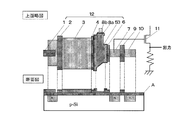
図1または図2において、Bは例えばp型Si(シリコン)よりなる半導体基板で、厚さ500μm程度である。半導体基板Bは例えばシリコン酸化膜の絶縁膜Aを有し、それを挟むようにして、電荷供給部1、電荷供給調整部2、センシング部3、障壁部4、センシング電荷蓄積部5、堰部6、フローティングディフュージョン7、リセットゲート8aおよび9、リセットドレイン8bおよび10、出力トランジスタ11が形成される。そして、電荷供給部1、電荷供給調整部2、センシング部3、障壁部4、リセットゲート8a、リセットドレイン8b、センシング電荷蓄積部5および堰部6の各部材によってセンサ部12が形成され、センサ部12、フローティングディフュージョン7、リセットゲート9およびリセットドレイン10によって検出部が形成される。半導体基板Bは、樹脂モールドなどを施すことにより溶液試料などに対して耐性をもたせている。
In FIG. 1 or FIG. 2, B is a semiconductor substrate made of, for example, p-type Si (silicon) and has a thickness of about 500 μm. The semiconductor substrate B has an insulating film A made of, for example, a silicon oxide film, and the
測定に際しては、電荷供給部1、障壁部4、堰部6、リセットゲート8aおよび9にパルス電圧を印加し、他の部位に直流電圧を印加し、p型半導体を用いたMOS構造において、正の電圧を加えることによって、半導体−絶縁膜界面近傍での電位状態を形成することができる。
In the measurement, in the MOS structure using a p-type semiconductor, a pulse voltage is applied to the
センサ部12は、例えば、次のようにして形成される。
(1)p型Si基板Bを熱酸化し、酸化膜(SiO2)を形成する。
(2)その一部分をエッチングし、その部分を選択的に酸化する。その後、その選択的に酸化された部分のSiO2をエッチングし、さらに熱酸化することによりゲート酸化膜Aを形成する。このゲート酸化膜の膜厚は約500Åである。
(3)その上面の電荷供給調整部2や障壁部4あるいは堰部6にそれぞれ対応する部分にリンドープされた低抵抗のポリシリコンを堆積させて電極を形成する。この電極の膜厚は約3000Åで、堆積させた後、約1000Å程度熱酸化する。
(4)その後、再びリンドープされた低抵抗のポリシリコンを堆積し、センシング電荷蓄積部5の上面に電極を形成する。この電極の膜厚は前記電極のそれと同程度に堆積させた後、約1000Å程度熱酸化する。このように酸化することにより、電極同士の絶縁が保たれる。この電極は、Al,W,Tiなどの金属電極でも代用できる。ただし、センシング電荷蓄積部5に電極が必要となるのは、半導体部分がp型基板の場合であり、図1に示すようなn拡散層の場合、この電極は必要ない。
(5)その後、Si3N4(Ta2O3またはAl2O3でもよい)を700Å程度堆積してセンシング部3を形成する。
The
(1) The p-type Si substrate B is thermally oxidized to form an oxide film (SiO 2 ).
(2) The part is etched and the part is selectively oxidized. Thereafter, the selectively oxidized portion of SiO 2 is etched and further thermally oxidized to form a gate oxide film A. The thickness of this gate oxide film is about 500 mm.
(3) Phosphorous-doped low-resistance polysilicon is deposited on portions corresponding to the charge
(4) Thereafter, phosphorus-doped low-resistance polysilicon is deposited again, and an electrode is formed on the upper surface of the sensing
(5) Thereafter, Si 3 N 4 (Ta 2 O 3 or Al 2 O 3 may be used) is deposited in a thickness of about 700 to form the
センシング部3は、物理的または化学的な量の大きさに対応して電位が変化する測定部位であり、例えばpH測定の場合には、水溶液や測定対象物などを導入するセルが設けられた電極部を形成し、試料中のpHに対応する電位を発生する。こうした電位あるいは電位の変化を電荷に変換し、検出部における電荷の変化を、MOS構造の出力トランジスタ11によって出力変換される。
The
ここで、電荷供給部1は、1のセンシング部3に対し1つに限定されるものではなく複数配設されていることが可能である。上述のように、測定対象あるいは用途によって、センシング部3の数量、形状あるいは配置関係が一義的に決定されることがあり、センシング部3全体への電荷の供給を迅速に行う必要がある場合において、センシング部3への電荷供給の負荷を複数の電荷供給部1に分散することが好ましい。
Here, the number of
センシング電荷蓄積部5は、センシング部3の形状あるいはセンシング部3とセンシング電荷蓄積部5との電荷容量比などによって設定されるが、図1では、センシング部との接触部分を大きくするとともに、センシング電荷蓄積部5の面積を小さくするために台形形状を形成している。また、センシング電荷蓄積部5は、n拡散層でも、p型基板そのままの状態でもよい。ただし、半導体部分がp型基板の場合は、上部に電極を設ける。
The sensing
また、フローティングディフュージョン7は、センシング電荷蓄積部5との接触部分を基に大きさが設定され、センシング電荷蓄積部5において放出される電荷を除く電荷が転送されることから、従来と比べ大幅に縮小することが可能となる。さらに、図1では、方形状となっているが、センシング電荷蓄積部5の形状が方形状であれば、センシング電荷蓄積部5との接触部分を大きくするとともにフローティングディフュージョン7の面積を小さくするために、台形形状などを形成することも可能である。
In addition, the size of the floating
上記のような測定装置における測定方法について、図3(A)に示す電位図を参照しながら説明する。
(1)初期電位状態
当初は、電荷供給部1の電位は高く(矢印方向が高い)設定されており、センシング部3には電荷は供給されていない。
(2)電荷の供給
電荷供給部1の電位を下げることによって、センシング部3に電荷を供給する。
(3)電荷の蓄積
電荷供給部1の電位を上げることによって、供給された電荷の一部がオーバーフローし電荷供給調整部2によって制限された量の電荷がセンシング部3に蓄積される。
このとき、センシング部3に蓄積された電荷量は、図3(B)に示すように、測定電荷量x以外にオフセット電荷yおよび外乱成分zが含まれる。
(4)電荷の転送1
障壁部4の電位を上げることによって、センシング部3に蓄積された電荷をセンシング電荷蓄積部5に転送する。
(5)電荷の転送2
障壁部4の電位を下げ、堰部6の電位を上げることによって、センシング電荷蓄積部5に蓄積された電荷の一部をフローティングディフュージョン7に転送する。このとき、転送された電荷量は主として測定電荷量xであるが、それ以外にオフセット電荷yあるいは外乱成分zが含まれる。
(6)電荷の放出
センシング電荷蓄積部5に蓄積された電荷は、リセットゲート8aの電位を上げることによってリセットドレイン8bを介して外部に放出する。
(7)蓄積のサイクル
フローティングディフュージョン7に所定量の電荷が蓄積するまで、上記(2)〜(6)を繰り返す。こうした繰り返しによって、外乱等のノイズの平均化を図ることができ、いわゆるランダムノイズについては実質的に削減することができる。また、この繰り返しの回数が、この検出系における実質的な増幅度となる。増幅度の正確な表記は後述する。
なお、堰部6は、電荷を繰り返し蓄積している間は同一状態とすることが可能である。その間のオフセット電荷の変動が少なければ、外乱ノイズの平均化およびオフセット電荷の補正が可能となる。
(8)電荷の測定
フローティングディフュージョン7に所定量の電荷が蓄積したときあるいは(7)蓄積のサイクルが予め設定した回数となったとき、堰部6の電位を下げて閉じ、電荷の流入を止める。この段階で、フローティングディフュージョン7の電位は転送されてきた電荷の量で決まるので、この電位をMOS構造の出力トランジスタ11のゲート部に入力し、この出力トランジスタ11のドレイン電流を測定する。
(9)リセット
フローティングディフュージョン7の電位を読み取った後、リセットゲート9をオンにしてリセットドレイン10から電荷を供出し、フローティングディフュージョン7の電位をリセットドレイン10の電位にリセットする。
(10)検出サイクル
上記のリセットにより、再び(1)と同じ状態に戻ることになる。つまり、検出サイクルとは、このように、(1)〜(9)の動作を繰り返すことをいい、これによって、センシング部3での電位の状態に対応した電荷量を順次出力することができる。
A measurement method in the measurement apparatus as described above will be described with reference to the potential diagram shown in FIG.
(1) Initial potential state Initially, the potential of the
(2) Supply of charge Charge is supplied to the
(3) Accumulation of Charge By raising the potential of the
At this time, as shown in FIG. 3B, the charge amount accumulated in the
(4)
By increasing the potential of the
(5)
A part of the charges accumulated in the sensing
(6) Release of charge The charge stored in the sensing
(7) Accumulation cycle The above (2) to (6) are repeated until a predetermined amount of electric charge is accumulated in the floating
The
(8) Measurement of charge When a predetermined amount of charge is accumulated in the floating
(9) Reset After reading the potential of the floating
(10) Detection cycle By the above reset, the same state as (1) is restored. That is, the detection cycle means that the operations (1) to (9) are repeated in this way, whereby the charge amount corresponding to the potential state in the
以上のように、この測定装置においては、物理的または化学的な量の大きさに対応して電位を変化するように構成されたセンシング部3を半導体基板Bに形成し、このセンシング部3に電荷を供給して、前記物理的または化学的な量をこのセンシング部の大きさに応じた電荷に変換するようにした電荷変換機構を用いている。このとき、センシング電荷蓄積部5に設けられたリセットゲート8aによって、オフセット電荷あるいは外乱成分を放出することができ、測定電荷量の検出にとってノイズとなる要素が極力少ない条件で検出することが可能となる。
As described above, in this measuring apparatus, the
上記測定における増幅度Aは、正確には下式1で表わすことができる。
〔式1〕
[Formula 1]
ここで、Q[C] :1回にフローティングディフュージョンに転送される電荷量
n[回] :蓄積回数
CFD[F] :フローティングディフュージョンの電荷容量
ΔVs :センシング部の電位変化
Where Q [C]: the amount of charge transferred to the floating diffusion at one time
n [times]: Number of times of accumulation
C FD [F]: Charge capacity of floating diffusion
ΔVs: Sensing potential change
なお、図3(A)では、電荷供給部1の電位を上げ下げしてセンシング部3に蓄積された電荷をすりきるようにしているが、これに代えて、図4に示すように、電荷供給部1の電位を一定に保持し、電荷供給調整部2の高さを上げ下げしてセンシング部3に電荷を蓄積するようにしてもよい。つまり、以下の操作によって、安定的に前記物理的または化学的な量をこのセンシング部の大きさに応じた電荷に変換することができる。
(1)初期電位状態
当初は、電荷供給部1の電位はセンシング部3より低く、電荷供給調整部2の電位はそれ以下に設定されており、センシング部3には電荷は供給されていない。
(2)電荷の供給
電荷供給調整部2の電位を、電荷供給部1の電位以上に上げることによって、センシング部3に電荷を供給する。
(3)電荷の蓄積
電荷供給調整部2の電位を(1)の状態にまで下げることによって、供給された電荷がセンシング部3に蓄積される。
(4)電荷の転送1
障壁部4の電位を上げることによって、センシング部3に蓄積された電荷をセンシング電荷蓄積部5に転送する。
(5)電荷の転送2
堰部6の電位を上げることによって、センシング電荷蓄積部5に蓄積された電荷の一部をフローティングディフュージョン7に転送する。このとき、転送された電荷量は主として測定電荷量であるが、それ以外にいくらかのオフセット電荷あるいは外乱成分が含まれる。
(6)電荷の放出
センシング電荷蓄積部5に蓄積された電荷は、リセットゲート9の電位を上げることによって外部に放出する。
(7)蓄積のサイクル
フローティングディフュージョン7に所定量の電荷が蓄積するまで、上記(2)〜(6)を繰り返す。こうした繰り返しによって、外乱等のノイズの平均化を図ることができ、いわゆるランダムノイズについては実質的に削減することができる。また、この繰り返しの回数が、この検出系における実質的な増幅度となる。
なお、堰部6は、電荷を繰り返し蓄積している間は同一状態とすることが可能である。その間のオフセット電荷の変動が少なければ、外乱ノイズの平均化およびオフセット電荷の補正が可能となる。
(8)電荷の測定
フローティングディフュージョン7に所定量の電荷が蓄積したときあるいは(7)蓄積のサイクルが予め設定した回数となったとき、堰部6の電位を下げて閉じ、電荷の流入を止める。この段階で、フローティングディフュージョン7の電位は転送されてきた電荷の量で決まるので、この電位をMOS構造の出力トランジスタ11のゲート部に入力し、この出力トランジスタ11のドレイン電流を測定する。
(9)リセット
フローティングディフュージョン7の電位を読み取った後、リセットゲート9をオンにしてリセットドレイン10から電荷を供出し、フローティングディフュージョン7の電位をリセットドレイン10の電位にリセットする。
(10)検出サイクル
上記のリセットにより、再び(1)と同じ状態に戻ることになる。つまり、検出サイクルとは、このように、(1)〜(9)の動作を繰り返すことをいい、これによって、センシング部3での電位の状態に対応した電荷量を順次出力することができる。図3(A)の方法の利点とともに、電荷供給部1の電位を基準とすることで一定電位を保持することが可能となり、さらに安定性の向上を図ることができる。また、図3(A)と同様、センシング部3に蓄積された電荷から、実質的に化学現象あるいは物理現象のみに対応する電荷量に近い電荷がフローティングディフュージョン7に転送されることによって、ノイズ成分の少ない電荷信号として処理することが可能となる。
In FIG. 3A, the potential of the
(1) Initial Potential State Initially, the potential of the
(2) Supply of charge Charge is supplied to the
(3) Accumulation of Charge The supplied charge is accumulated in the
(4)
By increasing the potential of the
(5)
By raising the potential of the
(6) Release of charge The charge accumulated in the sensing
(7) Accumulation cycle The above (2) to (6) are repeated until a predetermined amount of electric charge is accumulated in the floating
The
(8) Measurement of charge When a predetermined amount of charge is accumulated in the floating
(9) Reset After reading the potential of the floating
(10) Detection cycle By the above reset, the same state as (1) is restored. That is, the detection cycle means that the operations (1) to (9) are repeated in this way, whereby the charge amount corresponding to the potential state in the
また、本発明においては、センシング部3の電荷容量がフローティングディフュージョン7の電荷容量を超える大きさを有することが好ましい。例えば、上記の検出サイクルを繰り返し、フローティングディフュージョン7にある程度の電荷量が蓄積されてから電荷を測定するようにすることで、検出感度を上げることが可能であるが、その蓄積時間分だけ応答時間が遅くなる。センシング部3の電荷容量を大きくし蓄積される電荷を多くすることで、小電荷容量のフローティングディフュージョン7に転送された時のフローティングディフュージョン7での電位の変化率を上昇させることができることから、その変化率を検出することで、正確かつ感度の高い測定が可能となる。つまり、センシング部3と電荷転送手段であるフローティングディフュージョン7の間に電荷容量差を設けることによって、センシング部3のおける電位の変化の実質的に増幅機能を有することとなる。
In the present invention, it is preferable that the charge capacity of the
具体的にセンシング部3の電荷容量を大きくするには、(1)平面上での面積を大きくする、(2)センシング部3を複数にする、(3)電位を高くする、(4)電荷密度を上げる、などの手段があり、物理的または化学的な現象の対象となる試料の性状や濃度などによって選択することが可能である。
Specifically, to increase the charge capacity of the
また、上記半導体部分がp型基板の場合であって、センシング電荷蓄積部に電極を設けた場合を図4Aに例示する。第1構成例では、センシング電荷蓄積部5はn拡散層であり、電極は必要なかったが、図4Aの構成にあっては、n拡散層を形成せずp型基板のままで上部に電極を設け、センシング電荷蓄積部53を形成することによって、同様の動作ができる。この際の上部金属は、Al、Ti、Wなどの金属でも、poly−Siでもよい。なお、測定方法は、図3(A)と同様であり、省略する。
FIG. 4A illustrates a case where the semiconductor portion is a p-type substrate and an electrode is provided in the sensing charge storage portion. In the first configuration example, the sensing
次に、本発明における第2の構成例を説明する。第1構成例において、センシング部3の電位が予め設定された値よりも大きく低下(負の変化)する場合には、センシング電荷蓄積部5に蓄積される電荷量が小さく、閾部6からフローティングディフュージョン7に転送される電荷が測定電荷量xを下回る場合があり得る。このときセンシング部3の電位に対応した電荷をセンシング電荷蓄積部5に蓄積するために、図1における電荷供給調整部2に代えてセンシング部3を閾とし物理的または化学的な現象に対応して電荷蓄積量を可変できるようにしたものである。
Next, a second configuration example in the present invention will be described. In the first configuration example, when the potential of the
具体的には、図5に示すように、センシング部3の電位を閾とすることによって、センシング部3の電位が負の変化を生じた場合であっても、電荷供給部1からセンシング電荷蓄積部51に供給される電荷量を、センシング部3において生じる化学現象あるいは物理現象に対応して変化を取出すことができる。障壁部4、センシング電荷蓄積部52以降の構成および機能は第1構成例と同様である。なお、センシング部3の電位が安定的に変化する場合には、センシング電荷蓄積部51および障壁部4を省略し直接センシング電荷蓄積部52に電荷を蓄積することも可能である。
Specifically, as shown in FIG. 5, by setting the potential of the
上記のような測定装置における測定方法について、図6に示す電位図を参照しながら説明する。
(1)初期電位状態
当初は、電荷供給部1の電位は高く(矢印方向が高い)設定されており、センシング部電荷蓄積部51には電荷は供給されていない。
(2)電荷の供給
電荷供給部1の電位を下げることによって、センシング部3を閾としてセンシング部電荷蓄積部51に電荷を供給する。
(3)電荷の蓄積
電荷供給部1の電位を上げることによって、供給された電荷の一部がオーバーフローしセンシング部3を閾として制限された量の電荷がセンシング部電荷蓄積部51に蓄積される。このとき、センシング部電荷蓄積部51に蓄積された電荷量は、測定電荷量x以外にオフセット電荷yおよび外乱成分zが含まれる。
(4)電荷の転送1
障壁部4の電位を上げることによって、センシング部電荷蓄積部51に蓄積された電荷をセンシング電荷蓄積部52に転送する。
(5)電荷の転送2
障壁部4の電位を下げ、堰部6の電位を上げることによって、センシング電荷蓄積部52に蓄積された電荷の一部をフローティングディフュージョン7に転送する。このとき、転送された電荷量は主として測定電荷量xであるが、それ以外にオフセット電荷yあるいは外乱成分zが含まれる。
(6)電荷の放出
センシング電荷蓄積部52に蓄積された電荷は、リセットゲート8aの電位を上げることによってリセットドレイン8bを介して外部に放出する。
(7)蓄積のサイクル
フローティングディフュージョン7に所定量の電荷が蓄積するまで、上記(2)〜(6)を繰り返す。こうした繰り返しによって、外乱等のノイズの平均化を図ることができ、いわゆるランダムノイズについては実質的に削減することができる。また、この繰り返しの回数が、この検出系における実質的な増幅度となる。
(8)電荷の測定
フローティングディフュージョン7に所定量の電荷が蓄積したときあるいは(7)蓄積のサイクルが予め設定した回数となったとき、堰部6の電位を下げて閉じ、電荷の流入を止める。この段階で、フローティングディフュージョン7の電位は転送されてきた電荷の量で決まるので、この電位をMOS構造の出力トランジスタ11のゲート部に入力し、この出力トランジスタ11のドレイン電流を測定する。
(9)リセット
フローティングディフュージョン7の電位を読み取った後、リセットゲート9をオンにしてリセットドレイン10から電荷を供出し、フローティングディフュージョン7の電位をリセットドレイン10の電位にリセットする。
(10)検出サイクル
上記のリセットにより、再び(1)と同じ状態に戻ることになる。つまり、検出サイクルとは、このように、(1)〜(9)の動作を繰り返すことをいい、これによって、センシング部3での電位の状態に対応した電荷量を順次出力することができる。
A measuring method in the above measuring apparatus will be described with reference to the potential diagram shown in FIG.
(1) Initial Potential State Initially, the potential of the
(2) Supply of charge By lowering the potential of the
(3) Accumulation of charge By raising the potential of the
(4)
By increasing the potential of the
(5)
A part of the charges accumulated in the sensing
(6) Release of charge The charge stored in the sensing
(7) Accumulation cycle The above (2) to (6) are repeated until a predetermined amount of electric charge is accumulated in the floating
(8) Measurement of charge When a predetermined amount of charge is accumulated in the floating
(9) Reset After reading the potential of the floating
(10) Detection cycle By the above reset, the same state as (1) is restored. That is, the detection cycle means that the operations (1) to (9) are repeated in this way, whereby the charge amount corresponding to the potential state in the
以上のように、この測定装置においては、物理的または化学的な量の大きさに対応して電位を変化するように構成されたセンシング部3を半導体基板Bに形成し、このセンシング部3を閾として電荷を供給して、前記物理的または化学的な量をこの電荷移動量に変換するようにした電荷変換機構を用いている。このとき、センシング電荷蓄積部52に設けられたリセットゲート8aによって、オフセット電荷あるいは外乱成分を放出することができ、測定電荷量の検出にとってノイズとなる要素が極力少ない条件で検出することが可能となる。
As described above, in this measuring apparatus, the
なお、図5では、電荷供給部1の電位を上げ下げしてセンシング部3に蓄積された電荷をすりきるようにしているが、これに代えて、電荷供給部1の電位を一定に保持し、センシング部3の電位に対応してセンシング電荷蓄積部51に電荷を蓄積するようにしてもよい(図示せず)。
In FIG. 5, the potential of the
本発明における第3の構成例を図7に例示する。出力トランジスタ11の出力側にフィードバック回路13(制御部)を設け、出力トランジスタ11の出力が一定になるように電荷供給調整部2の電位を制御し、その制御量を測定値に変換する場合を表している。
A third configuration example of the present invention is illustrated in FIG. A case where a feedback circuit 13 (control unit) is provided on the output side of the
つまり、物理現象または化学現象を電荷情報に変換して定量化を行う場合においては、センシング部3あるいはフローティングディフュージョン7に残留する電荷の影響が無視できないことがある。具体的には、センシング部3からフローティングディフュージョン7までの電荷移動距離が長い場合あるいは検出サイクルの時間が短い場合では、電荷の移動が追いつかず電荷の一部がセンシング部3に残留することがある。このとき微小な電荷の移動を追跡する高感度測定においては、直線性、特にゼロ付近での直線性が悪くなることがある。そこで、本発明では、こうしたセンシング部3への電荷の残留を防止する、あるいは電荷の残留があっても検出特性に影響しないような電荷移動量に設定して、電荷移動量を一定にするように電荷供給調整部2の電位を調整するものである。
In other words, in the case where quantification is performed by converting physical phenomena or chemical phenomena into charge information, the influence of charges remaining in the
すなわち、電荷供給調整部2とセンシング部3との電位差を一定にすれば、センシング部3に供給される電荷供給量を一定にすることができ、電荷移動量が一定となる。このとき電荷移動量を所定値以上にすれば、上記の電荷の残留の影響は無視することができる。つまり、時間的にみれば、所定量を超える場合、転送パワーが落ちることから電荷の残留する(転送ロスの)確率が増加する。一方、実際の転送時に一定量の転送ロスが生じるとすれば、所定量よりも少ない場合には、その影響を無視することができない。
That is, if the potential difference between the charge
また、センシング部3からフローティングディフュージョン7に移動する電荷量が一定となり、その結果フローティングディフュージョン7の電位が一定となる。つまり、フローティングディフュージョン7に設けられた出力トランジスタ11の出力が一定となるように、物理現象または化学現象に伴うセンシング部3の電位の変化に対応して、電荷供給調整部2の電位を調整した場合、その調整量が物理現象または化学現象の変化に対応する測定量とすることができ、直線性を有する優れた検出特性を得ることができる。
Further, the amount of charge moving from the
また、センサ部12における電荷移動量を一定とすることで、センサ部12の変動要素を少なくし機能の安定化を図ることができる。さらに、センシング部3の特性にバラツキがあっても、同一試料についてのセンシング部3と電荷供給調整部2の電位差を一定にするように調節された電荷供給調整部2の電位を基準に、上記動作を行うことができる。従って、センシング部3の特性を厳格に規制することなく、同等の出力特性を得ることができる。
In addition, by making the amount of charge transfer in the
<デュアル式の物理現象または化学現象の測定装置の基本的な構成>
次に、上記物理現象または化学現象の基本的な測定装置を応用した、デュアル式の測定装置について、説明する。デュアル式の物理現象または化学現象の測定装置の基本的な構成を(第4構成例)を、図8に例示する。
<Basic configuration of a dual type physical or chemical measurement device>
Next, a dual type measuring apparatus to which the basic measuring apparatus for physical phenomena or chemical phenomena is applied will be described. FIG. 8 illustrates a basic configuration (fourth configuration example) of a dual type physical phenomenon or chemical phenomenon measurement apparatus.
基本的には、上記構成例の検出部を有する2つの並列する検出系を構成し、一方の堰部6aを他方のセンシング電荷蓄積部5bと接続し同電位にしている点に特徴を有している。1つの電荷供給部1および電荷供給調整部2を共用する2つの検出系からなり、一方の検出系Aは、物理現象または化学現象に対応して電位が変化するセンシング部3a、障壁部4a、センシング電荷蓄積部5a、堰部6a、フローティングディフュージョン7、リセットゲート8aおよび9、リセットドレイン8bおよび10、出力トランジスタ11から構成される。他方の検出系Bは、物理現象または化学現象に感応しないセンシング部3b、障壁部4b、センシング電荷蓄積部5b、堰部6bから構成される。このとき、センシング部3aと3bは、基本的には同様の構造を形成し物理現象または化学現象に対して異なる感応特性を有する膜あるいは部位を設けることが好ましい。オフセット電荷や外乱成分に対して同様の変化を生じることによって、検出系Bの補償機能を高めることができるためである。
Basically, it is characterized in that two parallel detection systems having the detection unit of the above-described configuration example are configured, and one
測定に際して、検出系Aの電荷信号は「検出信号+オフセット信号+外乱信号」に相当し検出系Bの電荷信号は「オフセット信号+外乱信号」に相当する。従って、両者の差を求めることで、真の「検出信号」を得ることができる。つまり、本発明においては、検出系Aのセンシング電荷蓄積部5aに蓄積されるべき電荷量が、上記検出系Aの電荷信号に相当し、検出系Bのセンシング電荷蓄積部5bに蓄積された電荷量が、上記検出系Bの電荷信号に相当する。ここで、検出系Aの堰部6aと検出系Bのセンシング電荷蓄積部5bとが同電位に接続されていることから、検出系Aのセンシング電荷蓄積部5aに蓄積されるべき電荷量のうち、検出系Bのセンシング電荷蓄積部5bに蓄積された電荷量を超える電荷量、つまり上記検出信号に相当する電荷量のみが、検出系Aの堰部6aを経由してフローティングディフュージョン7に転送されることになる。従って、検出系Bの補償機能を有効に生かして、真に必要とされる検出信号のみを精度よく取り出すことができる。
In the measurement, the charge signal of the detection system A corresponds to “detection signal + offset signal + disturbance signal”, and the charge signal of the detection system B corresponds to “offset signal + disturbance signal”. Therefore, a true “detection signal” can be obtained by obtaining the difference between the two. That is, in the present invention, the amount of charge to be accumulated in the sensing charge accumulation unit 5a of the detection system A corresponds to the charge signal of the detection system A, and the charge accumulated in the sensing
第4構成例における測定方法について、図9に示す電位図を参照しながら説明する。
(1)初期電位状態
当初は、電荷供給部1の電位は高く(矢印方向が高い)設定されており、センシング部3aおよび3bには電荷は供給されていない。
(2)電荷の供給
電荷供給部1の電位を下げることによって、センシング部3aおよび3bに電荷を供給する。
(3)電荷の蓄積
電荷供給部1の電位を上げることによって、供給された電荷の一部がオーバーフローし電荷供給調整部2によって制限された量の電荷がセンシング部3aおよび3bに蓄積される。このとき、検出系Aのセンシング部3aに蓄積された電荷量は、図3(B)に示すように、測定電荷量x以外にオフセット電荷yおよび外乱成分zが含まれ、検出系Bのセンシング部3bにはオフセット電荷yおよび外乱成分zに相当する電荷量が蓄積される。
(4)電荷の転送1
障壁部4aおよび4bの電位を上げることによって、センシング部3aおよび3bに蓄積された電荷をセンシング電荷蓄積部5aおよび5bに転送する。
このとき、検出系Aの障壁部4aの電位を検出系Bの障壁部4bよりも少し遅れて上げることが好ましい。堰部6aの電位はセンシング電荷蓄積部5bの電位と同じレベルとなることから、センシング電荷蓄積部5bに蓄積する電荷量の増加に合せて堰部6aの電位が徐々に低下する。従って、障壁部4aの電位が障壁部4bよりも少し遅れて上がることによって、まず検出系Aの堰部6bの電位が上昇し、センシング部3aからの電荷を蓄積するスペースを作ることによって、フローティングディフュージョン7に漏れて転送されることを防止することができる。遅延時間は、予め測定電荷量x、オフセット電荷yおよび外乱成分zを測定あるいは予測することで設定することができる。
(5)電荷の蓄積
障壁部4aおよび4bの電位を下げることによって、転送された電荷がセンシング電荷蓄積部5aおよび5bに蓄積される。このとき、検出系Bのセンシング電荷蓄積部5bの電荷量には、オフセット電荷yあるいは外乱成分zが含まれる。一方、検出系Aのセンシング電荷蓄積部5aに蓄積される電荷量は、本来的には、測定電荷量xに加えオフセット電荷yあるいは外乱成分zが含まれることになる。
(6)電荷の転送2
しかし、堰部6aの電位がセンシング電荷蓄積部5bの電位以下になることがないことから、測定電荷量xが堰部6aをオーバーフローすることによって、フローティングディフュージョン7に転送する。
(7)電荷の放出
検出系Aのセンシング電荷蓄積部5aに蓄積された電荷は、リセットゲート8aの電位を上げることによって外部に放出する。検出系Bのセンシング電荷蓄積部5bに蓄積された電荷は、堰部6bの電位を上げることによって外部に放出する。
(8)蓄積のサイクル
フローティングディフュージョン7に所定量の電荷が蓄積するまで、上記(2)〜(7)を繰り返す。こうした繰り返しによって、外乱等のノイズの平均化を図ることができ、いわゆるランダムノイズについては実質的に削減することができる。また、この繰り返しの回数が、この検出系における実質的な増幅度となる。特に、本発明においては、検出電荷量のみを抽出して蓄積できることから、S/N比は非常に向上する。
(9)電荷の測定
フローティングディフュージョン7に所定量の電荷が蓄積したときあるいは(8)蓄積のサイクルが予め設定した回数となったとき、堰部6aの電位を下げて閉じ、電荷の流入を止める。この段階で、フローティングディフュージョン7の電位は転送されてきた電荷の量で決まるので、この電位をMOS構造の出力トランジスタ11のゲート部に入力し、この出力トランジスタ11のドレイン電流を測定する。
(10)リセット
フローティングディフュージョン7の電位を読み取った後、リセットゲート9をオンにしてリセットドレイン10から電荷を供出し、フローティングディフュージョン7の電位をリセットドレイン10の電位にリセットする。
(11)検出サイクル
上記のリセットにより、再び(1)と同じ状態に戻ることになる。つまり、検出サイクルとは、このように、(1)〜(10)の動作を繰り返すことをいい、これによって、センシング部3aでの電位の状態に対応した電荷量を順次出力することができる。
The measurement method in the fourth configuration example will be described with reference to the potential diagram shown in FIG.
(1) Initial potential state Initially, the electric potential of the
(2) Supply of charge Charge is supplied to the
(3) Accumulation of Charge By raising the potential of the
(4)
By increasing the potentials of the
At this time, it is preferable that the potential of the
(5) Accumulation of charges By lowering the potentials of the
(6)
However, since the potential of the
(7) Release of charge The charge accumulated in the sensing charge accumulation unit 5a of the detection system A is released to the outside by raising the potential of the
(8) Accumulation cycle The above (2) to (7) are repeated until a predetermined amount of electric charge is accumulated in the floating
(9) Measurement of charge When a predetermined amount of charge is accumulated in the floating
(10) Reset After reading the potential of the floating
(11) Detection cycle By the above reset, the same state as (1) is restored. That is, the detection cycle means that the operations (1) to (10) are repeated in this way, whereby the charge amount corresponding to the potential state in the
以上のように、この測定装置においては、物理的または化学的な量の大きさに対応して電位を変化するように構成されたセンシング部3aからの電荷から、ノイズ成分であるオフセット電荷および外乱成分を除去した電荷量を取り出すことによって、測定電荷量の検出にとってノイズとなる要素が極力少ない条件で検出することが可能となる。
As described above, in this measuring apparatus, the offset charge and the disturbance, which are noise components, from the charge from the
なお、図9では、電荷供給部1の電位を上げ下げしてセンシング部3に蓄積された電荷をすりきるようにしているが、これに代えて、電荷供給部1の電位を一定に保持し、電荷供給調整部2の高さを上げ下げしてセンシング部3aおよび3bに電荷を蓄積するようにしてもよい(図示せず)。
In FIG. 9, the potential of the
また、第4構成例では各検出系を第1構成例の構成を基本としているが、各検出系を第2構成例の構成を基本にした場合を第5構成例として説明する。
図10に例示するように、基本構成は第4構成例と同様であるが、電荷供給調整部2に代えて、2つの検出系AおよびBの対となるセンシング部3aおよび3bを閾としてセンシング電荷蓄積部51aおよび51bに供給する電荷量を決定する構成を有する点において相違する。
In the fourth configuration example, each detection system is based on the configuration of the first configuration example. However, a case where each detection system is based on the configuration of the second configuration example will be described as a fifth configuration example.
As illustrated in FIG. 10, the basic configuration is the same as that of the fourth configuration example. However, instead of the charge
つまり、センシング部3aおよび3bの電位が、化学現象あるいは物理現象に対応してあるいはオフセットの変化や外乱によって負の変化を生じた場合であっても、電荷供給部1からセンシング電荷蓄積部51aおよび51bに供給される電荷量を、検出系Aではセンシング部3aを閾とすることで化学現象あるいは物理現象に対応して変化を取出すことができ、検出系Bではセンシング部3bを閾とすることで化学現象あるいは物理現象に対応しない変化を取出すことができる。
That is, even if the potentials of the
このとき、図10に示すように、センシング電荷蓄積部51aおよび51bが同電位であることが好ましい。各検出系のオフセット電荷yを等しくすることができることから、補正機能を高めることができるためである。
At this time, as shown in FIG. 10, it is preferable that the sensing
具体的には、検出系Aにおいてセンシング電荷蓄積部51aに供給された電荷量は主として測定電荷量xであるが、それ以外にオフセット電荷yあるいは外乱成分zが含まれる。他方、検出系Bにおいてセンシング電荷蓄積部51aに供給された電荷量はオフセット電荷yあるいは外乱成分zが含まれる。従って、センシング電荷蓄積部51aおよび51bから転送された各々の電荷量について、検出系Aの堰部6aと検出系Bのセンシング電荷蓄積部52bとが同電位に接続されていることから、検出系Aのセンシング電荷蓄積部52aに蓄積されるべき電荷量のうち、検出系Bのセンシング電荷蓄積部52bに蓄積された電荷量を超える電荷量、つまり上記測定電荷量xのみが、検出系Aの堰部6aを経由してフローティングディフュージョン7に転送されることになる。従って、検出系Bの補償機能を有効に生かして、真に必要とされる測定電荷量xつまり測定における検出信号のみを精度よく取り出すことができる。
Specifically, the amount of charge supplied to the sensing
さらに、1つのフローティングディフュージョンに対し電荷転送部を介して複数のセンサ部からの電荷を順次移動させるCCD機能を有することによって、物理的または化学的な現象の一次元分布または二次元分布を容易に画像化することができる。具体的には、図11に例示するような第6構成例が可能である。 Furthermore, by having a CCD function that sequentially moves charges from a plurality of sensor units via a charge transfer unit for one floating diffusion, one-dimensional distribution or two-dimensional distribution of a physical or chemical phenomenon can be easily performed. Can be imaged. Specifically, a sixth configuration example illustrated in FIG. 11 is possible.
つまり、複数のセンサ部12(a,a)、12(a,b)、・・・と、各センサ部において変換された電荷を矢印方向に転送する電荷転送部16と、転送されてきた電荷をさらに転送する1つのフローティングディフュージョン7と、転送されてきた電荷を出力信号に変換する出力トランジスタ11とからなる。
That is, the plurality of sensor units 12 (a, a), 12 (a, b),..., The
センサ部12(a,a)、12(a,b)、・・・を一次元的あるいは二次元的に配置してアレイ化することにより、複数点の情報を同時に取り込み、電荷転送部16および出力トランジスタ11によって、複数点の信号を秩序よく処理することができる。出力された信号は、そのままCRTなどの画像出力装置(図示せず)に入力して画像出力したり、出力信号をAD変換してコンピュータに入力することができる。
The sensor units 12 (a, a), 12 (a, b),... Are arranged one-dimensionally or two-dimensionally to form an array, so that information on a plurality of points can be simultaneously acquired, and the
つまり、各センサ部12(a,a)、12(a,b)、・・・と電荷転送部16との接合部におけるゲートを順次開として蓄積された電荷を供出し、CCD駆動電位を順にON−OFFすることによって電荷転送部16の転送路を経由して転送される。このとき、電荷転送部16におけるCCDの駆動は、一相駆動、二相駆動あるいは四相駆動など、転送される電荷量に応じて適宜選定することができる。なお、センサ部12の数が多くなるに伴って転送効率が大きな問題となるが、その場合は、転送経路として転送効率の高いバルクチャンネルを用いるのが好ましい。転送されてきた電位は、フローティングディフュージョン7に転送され、このフローティングディフュージョン7の電位を変化させる。この電位の変化を、出力トランジスタ11のゲートに入力し、検出出力とする。
That is, the accumulated charges are supplied by sequentially opening the gates at the junctions of the sensor units 12 (a, a), 12 (a, b),... It is transferred via the transfer path of the
CCDは、S/N比の高さ、転送速度、転送効率および操作性の点で優れた特性を有しており、複数の電極を作動させる場合において非常に有用である。つまり、CCDを構成する複数の電極が、上記のセンシング電荷蓄積部5あるいは障壁部4や堰部6の機能を果たすことが可能であり、転送の迅速化が可能である点においても優位である。さらに、各電極に印加する電圧に差を設ける必要がないことからセンシング部3とフローティングディフュージョン7間の電位差を制限したり、電極数を制限する必要がない点においても有用である。また、CCDは、センシング部3に蓄積された電荷量に応じて、電荷転送時に、同時に稼動させる電極数を変更することによって、最適条件で電荷を転送することが可能である。つまり、転送する電荷量が多い場合には複数の電極を稼動することによって、電荷の未転送をなくすことができる。さらに、転送する電荷量が少ない場合には1つの電極を稼動することによって、電極部における残留電荷をなくし、測定誤差要因をなくすことができる。
The CCD has excellent characteristics in terms of high S / N ratio, transfer speed, transfer efficiency, and operability, and is very useful when operating a plurality of electrodes. That is, the plurality of electrodes constituting the CCD can perform the functions of the sensing
上記では、各請求項に係る発明によって形成される機能を、一部組合せた構成例を挙げて説明したが、むろん、本発明はこれに限定されるものではなく、他の組合せ、あるいは本願に記載の事項との任意の組合せが可能であることはいうまでもない。 In the above, the functions formed by the invention according to each claim have been described with reference to a configuration example in which a part of the functions is combined. However, the present invention is not limited to this, and other combinations, or the present application is included. It goes without saying that any combination with the matters described is possible.
以上、この発明は、広く溶液などサンプルのイオン濃度の二次元分布測定に好適に用いることができるほか、以下のような分野にも適用することができる。
(1)化学顕微鏡としての応用分野・化学;イオン濃度計測・電気化学的分野、ガス分布計測分野・滴定の二次元的動的観察および解析
(2)環境計測・環境;バイオリメディエーションへの適用
(3)食品検査・食品、微生物
(4)ME分野・医学・生態組織;組織細胞の表面イオン濃度計測、細胞表面電位計測、DNA計測
(5)バイオ分野
(6)動植物分野・植物;カルスの表面電位分布計測・生物・正面図動物
(7)腐蝕計測分野・金属;金属腐蝕と塗装・コーティング
(8)ゼータ電位等表面解析・粉体、セラミックスのゼータ電位。
As described above, the present invention can be widely used for measuring the two-dimensional distribution of the ion concentration of a sample such as a solution, and can also be applied to the following fields.
(1) Chemical microscope application fields / chemistry; ion concentration measurement / electrochemical field, gas distribution measurement field / two-dimensional dynamic observation and analysis of titration (2) environmental measurement / environment; application to bioremediation ( 3) Food inspection / food, microorganisms (4) ME field / medicine / ecological tissue; surface ion concentration measurement of tissue cells, cell surface potential measurement, DNA measurement (5) bio field (6) animal and plant field / plant; callus surface Potential distribution measurement, organisms, front view animals (7) Corrosion measurement field, metal; metal corrosion and coating, coating (8) Surface analysis such as zeta potential, zeta potential of powder and ceramics.
また、測定対象(サンプル)は、気体、液体、固体、粉体のいずれであってもよく、センサ部の特定感応層により選択的に反応する化学センシングと、物理的接触による界面現象に電荷変動をするあらゆる現象に適用でき、例えば液の流れや一瞬の化学反応の過渡現象の分布を高感度、高画質の化学画像として得ることができる。さらに、滴定現象のリアルタイム画像化から画像ソフトによる他の種類の解析、表示にも有用であり、携帯化カメラにも有効である。 In addition, the measurement target (sample) may be any of gas, liquid, solid, and powder. Chemical fluctuation that reacts selectively by the specific sensitive layer of the sensor part and the charge fluctuation due to the interface phenomenon due to physical contact For example, the distribution of a liquid flow or transient chemical reaction transients can be obtained as a high-sensitivity, high-quality chemical image. Furthermore, it is useful for real-time imaging of titration phenomena to other types of analysis and display using image software, and is also effective for portable cameras.
1 電荷供給部
2 電荷供給調整部
3、3a、3b センシング部
4、4a、4b 障壁部
5、5a、5b、51、51a、51b、52、52a、52b センシング電荷蓄積部
6、6a、6b 堰部
7 フローティングディフュージョン
8a、9 リセットゲート
8b、10 リセットドレイン
11 出力トランジスタ
12 センサ部
13 フィードバック回路
14 導体
15 電極部
16 電荷転送部
A 絶縁膜
B 半導体基板
DESCRIPTION OF
Claims (7)
前記センシング部からの電荷をフローティングディフュージョンの前段で蓄積し、その一部を放出するとともに、物理的または化学的な量の大きさに対応する電位に相当する電荷を含む電荷量をフローティングディフュージョンに転送すること、および前記放出量を変更可能とすることを特徴とする物理現象または化学現象の測定方法。 Charge is supplied from the charge supply unit to the sensing unit whose potential changes according to the physical or chemical quantity, and the supplied charge is taken out from the sensing unit via the floating diffusion and supplied. A method of measuring the physical or chemical phenomenon by detecting the amount of charge, comprising:
The charge from the sensing unit is accumulated in the front stage of the floating diffusion, and a part of the charge is discharged, and the charge amount including the charge corresponding to the potential corresponding to the magnitude of the physical or chemical amount is transferred to the floating diffusion. And a method of measuring a physical phenomenon or a chemical phenomenon, wherein the release amount is changeable.
前記センシング部からの電荷をフローティングディフュージョンの前段で蓄積し、その一部を放出するとともに、物理的または化学的な量の大きさに対応する電位に相当する電荷を含む電荷量をフローティングディフュージョンに転送すること、および前記放出量を変更可能とすることを特徴とする物理現象または化学現象の測定方法。 Charge is supplied from the charge supply unit using the sensing unit whose potential changes according to the magnitude of the physical or chemical amount as a threshold, and the supplied charge is taken out from the sensing unit via the floating diffusion and supplied. A method of measuring the physical or chemical phenomenon by detecting the amount of charge, comprising:
The charge from the sensing unit is accumulated in the front stage of the floating diffusion, and a part of the charge is discharged, and the charge amount including the charge corresponding to the potential corresponding to the magnitude of the physical or chemical amount is transferred to the floating diffusion. And a method of measuring a physical phenomenon or a chemical phenomenon, wherein the release amount is changeable.
前記センシング部とフローティングディフュージョンの中間に、
該センシング部から転送された電荷を蓄積するとともに、蓄積された電荷の一部を放出するリセットゲートを有するセンシング電荷蓄積部、
および残りの電荷をフローティングディフュージョンに転送する堰部、
を有することを特徴とする物理現象または化学現象の測定装置。 A charge supply unit that supplies charge to the sensing unit; a sensing unit that changes in potential according to a physical or chemical quantity; and a detection unit that includes a floating diffusion that extracts the charge supplied to the sensing unit. A measuring device,
Between the sensing unit and the floating diffusion,
A sensing charge accumulator having a reset gate for accumulating the charge transferred from the sensing unit and releasing a part of the accumulated charge;
And a weir that transfers the remaining charge to the floating diffusion,
An apparatus for measuring a physical phenomenon or a chemical phenomenon, characterized by comprising:
前記センシング部とフローティングディフュージョンの中間に、
該センシング部から転送された電荷を蓄積するとともに、蓄積された電荷の一部を放出するリセットゲートを有するセンシング電荷蓄積部、
および残りの電荷をフローティングディフュージョンに転送する堰部、
を有することを特徴とする物理現象または化学現象の測定装置。 A detection unit comprising a charge supply unit that supplies charges to the sensing unit, a sensing unit that changes in potential according to the magnitude of a physical or chemical amount, and a floating diffusion that takes out the supplied charge using the sensing unit as a threshold A measuring device comprising:
Between the sensing unit and the floating diffusion,
A sensing charge accumulator having a reset gate for accumulating the charge transferred from the sensing unit and releasing a part of the accumulated charge;
And a weir that transfers the remaining charge to the floating diffusion,
An apparatus for measuring a physical phenomenon or a chemical phenomenon, characterized by comprising:
物理的または化学的な量の大きさに対応して電位が変化するセンシング部を有し、センシング部に供給された電荷の一部がセンシング電荷蓄積部および堰部を介してフローティングディフュージョンに転送される検出系Aと、
物理的または化学的な量の変化に感応しないセンシング部を有し、センシング部以外の機能を検出系Aと同じくする検出系Bからなるとともに、
検出系Bのセンシング電荷蓄積部に蓄積された電荷量に連動して、検出系Aの堰部から転送する電荷量を変化させることを特徴とする請求項4または5記載の物理現象または化学現象の測定装置。 A measurement apparatus having at least a pair of detection systems having the charge supply unit, the sensing charge storage unit, and the reset gate having the same structure,
It has a sensing unit whose potential changes according to the physical or chemical quantity, and part of the charge supplied to the sensing unit is transferred to the floating diffusion through the sensing charge storage unit and weir unit. Detection system A,
It has a sensing unit that is not sensitive to changes in physical or chemical quantities, and comprises a detection system B that has the same function as the detection system A except for the sensing unit,
6. The physical or chemical phenomenon according to claim 4 or 5, wherein the amount of charge transferred from the weir portion of the detection system A is changed in conjunction with the amount of charge accumulated in the sensing charge accumulation portion of the detection system B. Measuring device.
Priority Applications (3)
| Application Number | Priority Date | Filing Date | Title |
|---|---|---|---|
| JP2005225505A JP4678676B2 (en) | 2004-12-10 | 2005-08-03 | Method or apparatus for measuring physical or chemical phenomena |
| US11/289,819 US7424372B2 (en) | 2004-12-10 | 2005-11-29 | Method and apparatus for measuring physical or chemical phenomena |
| EP05027011A EP1669749A1 (en) | 2004-12-10 | 2005-12-09 | FET based method and apparatus for measuring physical or chemical phenomena |
Applications Claiming Priority (2)
| Application Number | Priority Date | Filing Date | Title |
|---|---|---|---|
| JP2004358803 | 2004-12-10 | ||
| JP2005225505A JP4678676B2 (en) | 2004-12-10 | 2005-08-03 | Method or apparatus for measuring physical or chemical phenomena |
Publications (2)
| Publication Number | Publication Date |
|---|---|
| JP2006189416A JP2006189416A (en) | 2006-07-20 |
| JP4678676B2 true JP4678676B2 (en) | 2011-04-27 |
Family
ID=35985424
Family Applications (1)
| Application Number | Title | Priority Date | Filing Date |
|---|---|---|---|
| JP2005225505A Expired - Fee Related JP4678676B2 (en) | 2004-12-10 | 2005-08-03 | Method or apparatus for measuring physical or chemical phenomena |
Country Status (3)
| Country | Link |
|---|---|
| US (1) | US7424372B2 (en) |
| EP (1) | EP1669749A1 (en) |
| JP (1) | JP4678676B2 (en) |
Families Citing this family (30)
| Publication number | Priority date | Publication date | Assignee | Title |
|---|---|---|---|---|
| KR101343044B1 (en) * | 2005-03-11 | 2013-12-18 | 고꾸리쯔 다이가꾸 호우징 도요하시 기쥬쯔 가가꾸 다이가꾸 | Cumulative chemical/physical phenomenon detecting apparatus |
| US8262900B2 (en) | 2006-12-14 | 2012-09-11 | Life Technologies Corporation | Methods and apparatus for measuring analytes using large scale FET arrays |
| CN101669026B (en) | 2006-12-14 | 2014-05-07 | 生命技术公司 | Methods and apparatus for measuring analytes using large scale FET arrays |
| US11339430B2 (en) | 2007-07-10 | 2022-05-24 | Life Technologies Corporation | Methods and apparatus for measuring analytes using large scale FET arrays |
| JP5077799B2 (en) * | 2008-03-25 | 2012-11-21 | 国立大学法人豊橋技術科学大学 | Chemical / physical phenomenon detection apparatus and control method thereof |
| US20100137143A1 (en) | 2008-10-22 | 2010-06-03 | Ion Torrent Systems Incorporated | Methods and apparatus for measuring analytes |
| US20100301398A1 (en) | 2009-05-29 | 2010-12-02 | Ion Torrent Systems Incorporated | Methods and apparatus for measuring analytes |
| US8776573B2 (en) | 2009-05-29 | 2014-07-15 | Life Technologies Corporation | Methods and apparatus for measuring analytes |
| US8858782B2 (en) | 2010-06-30 | 2014-10-14 | Life Technologies Corporation | Ion-sensing charge-accumulation circuits and methods |
| CN109449171A (en) | 2010-06-30 | 2019-03-08 | 生命科技公司 | For detecting and measuring the transistor circuit of chemical reaction and compound |
| JP5952813B2 (en) * | 2010-06-30 | 2016-07-13 | ライフ テクノロジーズ コーポレーション | Method and apparatus for testing ISFET arrays |
| US11307166B2 (en) | 2010-07-01 | 2022-04-19 | Life Technologies Corporation | Column ADC |
| WO2012006222A1 (en) | 2010-07-03 | 2012-01-12 | Life Technologies Corporation | Chemically sensitive sensor with lightly doped drains |
| WO2012036679A1 (en) | 2010-09-15 | 2012-03-22 | Life Technologies Corporation | Methods and apparatus for measuring analytes |
| WO2013008908A1 (en) * | 2011-07-14 | 2013-01-17 | 国立大学法人豊橋技術科学大学 | Method for detecting chemical and physical phenomenon, and device therefor |
| US9970984B2 (en) | 2011-12-01 | 2018-05-15 | Life Technologies Corporation | Method and apparatus for identifying defects in a chemical sensor array |
| US9080968B2 (en) | 2013-01-04 | 2015-07-14 | Life Technologies Corporation | Methods and systems for point of use removal of sacrificial material |
| US9841398B2 (en) | 2013-01-08 | 2017-12-12 | Life Technologies Corporation | Methods for manufacturing well structures for low-noise chemical sensors |
| US8963216B2 (en) | 2013-03-13 | 2015-02-24 | Life Technologies Corporation | Chemical sensor with sidewall spacer sensor surface |
| US20140264472A1 (en) | 2013-03-15 | 2014-09-18 | Life Technologies Corporation | Chemical sensor with consistent sensor surface areas |
| WO2014149779A1 (en) | 2013-03-15 | 2014-09-25 | Life Technologies Corporation | Chemical device with thin conductive element |
| US9835585B2 (en) | 2013-03-15 | 2017-12-05 | Life Technologies Corporation | Chemical sensor with protruded sensor surface |
| US10458942B2 (en) | 2013-06-10 | 2019-10-29 | Life Technologies Corporation | Chemical sensor array having multiple sensors per well |
| JP6228098B2 (en) * | 2014-10-20 | 2017-11-08 | シャープ株式会社 | Chemical / physical phenomenon detection device and manufacturing method thereof |
| WO2016100486A1 (en) | 2014-12-18 | 2016-06-23 | Life Technologies Corporation | High data rate integrated circuit with transmitter configuration |
| US10077472B2 (en) | 2014-12-18 | 2018-09-18 | Life Technologies Corporation | High data rate integrated circuit with power management |
| EP3273233B8 (en) * | 2015-03-19 | 2022-08-03 | National University Corporation Toyohashi University Of Technology | Method for controlling a chemical/physical phenomenon detecting device |
| JP7300185B2 (en) * | 2018-05-25 | 2023-06-29 | 公立大学法人大阪 | chemical sensor |
| JP2020094913A (en) * | 2018-12-13 | 2020-06-18 | 国立大学法人豊橋技術科学大学 | pH detector |
| US11913971B2 (en) * | 2021-02-24 | 2024-02-27 | Globalfoundries U.S. Inc. | Motion-sensitive field effect transistor, motion detection system, and method |
Citations (10)
| Publication number | Priority date | Publication date | Assignee | Title |
|---|---|---|---|---|
| JPH09233392A (en) * | 1996-02-27 | 1997-09-05 | Canon Inc | Photoelectric converter |
| JPH10150183A (en) * | 1996-09-20 | 1998-06-02 | Sony Corp | Solid-state image sensing device, its driving method and camera |
| JPH10332423A (en) * | 1997-05-29 | 1998-12-18 | Horiba Ltd | Method and device for measuring physical phenomenon or chemical phenomenon |
| JP2000065786A (en) * | 1998-08-20 | 2000-03-03 | Horiba Ltd | APPARATUS FOR MEASURING pH DISTRIBUTION OF ELECTROLYTE |
| JP2001050897A (en) * | 1999-08-10 | 2001-02-23 | Horiba Ltd | Chemical two-dimensional distribution-measuring device |
| JP2001244454A (en) * | 2000-02-29 | 2001-09-07 | Horiba Ltd | Molecule recognition type electrochemical ccd device |
| JP2002098667A (en) * | 2000-09-27 | 2002-04-05 | Japan Science & Technology Corp | Cumulative chemical and physical phenomenon detector |
| JP2003014691A (en) * | 2001-06-29 | 2003-01-15 | Horiba Ltd | Ccd sensor |
| WO2003042683A1 (en) * | 2001-11-16 | 2003-05-22 | Bio-X Inc. | Fet type sensor, ion density detecting method comprising this sensor, and base sequence detecting method |
| JP2004032682A (en) * | 2002-04-08 | 2004-01-29 | Matsushita Electric Works Ltd | Free space information detector using intensity modulated light |
Family Cites Families (6)
| Publication number | Priority date | Publication date | Assignee | Title |
|---|---|---|---|---|
| JP2571016B2 (en) | 1994-04-27 | 1997-01-16 | 日本電気株式会社 | Method of manufacturing gas discharge display panel |
| JP3608903B2 (en) | 1997-04-02 | 2005-01-12 | パイオニア株式会社 | Driving method of surface discharge type plasma display panel |
| US5852347A (en) * | 1997-09-29 | 1998-12-22 | Matsushita Electric Industries | Large-area color AC plasma display employing dual discharge sites at each pixel site |
| US5998935A (en) * | 1997-09-29 | 1999-12-07 | Matsushita Electric Industrial Co., Ltd. | AC plasma display with dual discharge sites and contrast enhancement bars |
| JP4183789B2 (en) | 1998-01-14 | 2008-11-19 | 株式会社堀場製作所 | Detection device for physical and / or chemical phenomena |
| EP1443991A4 (en) | 2001-11-13 | 2007-03-14 | Applied Med Resources | Multi-seal trocar system |
-
2005
- 2005-08-03 JP JP2005225505A patent/JP4678676B2/en not_active Expired - Fee Related
- 2005-11-29 US US11/289,819 patent/US7424372B2/en not_active Expired - Fee Related
- 2005-12-09 EP EP05027011A patent/EP1669749A1/en not_active Withdrawn
Patent Citations (10)
| Publication number | Priority date | Publication date | Assignee | Title |
|---|---|---|---|---|
| JPH09233392A (en) * | 1996-02-27 | 1997-09-05 | Canon Inc | Photoelectric converter |
| JPH10150183A (en) * | 1996-09-20 | 1998-06-02 | Sony Corp | Solid-state image sensing device, its driving method and camera |
| JPH10332423A (en) * | 1997-05-29 | 1998-12-18 | Horiba Ltd | Method and device for measuring physical phenomenon or chemical phenomenon |
| JP2000065786A (en) * | 1998-08-20 | 2000-03-03 | Horiba Ltd | APPARATUS FOR MEASURING pH DISTRIBUTION OF ELECTROLYTE |
| JP2001050897A (en) * | 1999-08-10 | 2001-02-23 | Horiba Ltd | Chemical two-dimensional distribution-measuring device |
| JP2001244454A (en) * | 2000-02-29 | 2001-09-07 | Horiba Ltd | Molecule recognition type electrochemical ccd device |
| JP2002098667A (en) * | 2000-09-27 | 2002-04-05 | Japan Science & Technology Corp | Cumulative chemical and physical phenomenon detector |
| JP2003014691A (en) * | 2001-06-29 | 2003-01-15 | Horiba Ltd | Ccd sensor |
| WO2003042683A1 (en) * | 2001-11-16 | 2003-05-22 | Bio-X Inc. | Fet type sensor, ion density detecting method comprising this sensor, and base sequence detecting method |
| JP2004032682A (en) * | 2002-04-08 | 2004-01-29 | Matsushita Electric Works Ltd | Free space information detector using intensity modulated light |
Also Published As
| Publication number | Publication date |
|---|---|
| EP1669749A1 (en) | 2006-06-14 |
| JP2006189416A (en) | 2006-07-20 |
| US7424372B2 (en) | 2008-09-09 |
| US20060129332A1 (en) | 2006-06-15 |
Similar Documents
| Publication | Publication Date | Title |
|---|---|---|
| JP4678676B2 (en) | Method or apparatus for measuring physical or chemical phenomena | |
| JP2006284225A (en) | Potential measuring method and measuring instrument | |
| JP4231560B2 (en) | Method and apparatus for electrochemical measurement of chemical quantity distribution | |
| JP5890423B2 (en) | ISFET device | |
| Hizawa et al. | Fabrication of a two-dimensional pH image sensor using a charge transfer technique | |
| Sawada et al. | Highly sensitive ion sensors using charge transfer technique | |
| US11008611B2 (en) | Double gate ion sensitive field effect transistor | |
| Matsuo et al. | Charge Transfer Type pH Sensor with Super High Sensitivity | |
| TWI465716B (en) | Transistor circuits for detection and measurement of chemical reactions and compounds | |
| JP4641444B2 (en) | Potential measurement device for physical or chemical phenomena | |
| Moser et al. | ISFET arrays for lab-on-chip technology: A review | |
| Prodromakis et al. | A low-cost disposable chemical sensing platform based on discrete components | |
| JP5553316B2 (en) | Spectroscopic apparatus and control method thereof | |
| Jiang et al. | A 512× 576 65-nm CMOS ISFET sensor for food safety screening with 123.8 mV/pH sensitivity and 0.01 pH resolution | |
| Takenaga et al. | Charge accumulation type hydrogen ion image sensor with high pH resolution | |
| Teng et al. | Sensing characteristic enhancement of CMOS-based ISFETs with three-dimensional extended-gate architecture | |
| WO2005123228A2 (en) | Ccd imaging array with improved charge sensing circuit | |
| JP2005337806A (en) | Measuring method or physical or chemical phenomenon or its measuring instrument | |
| JP4700335B2 (en) | Method and apparatus for measuring physical or chemical phenomena | |
| Zeng et al. | Current-mode ISFET array with row-parallel ADCs for ultra-high speed ion imaging | |
| JP6307058B2 (en) | Ion concentration sensor and ion concentration measuring method | |
| WO2019230917A1 (en) | Ion concentration measuring device | |
| Liou et al. | high resolution ion detector (hrid) by 16nm finfet cmos technology | |
| JP2003014691A (en) | Ccd sensor | |
| CN215404243U (en) | Gene sequencing sensing device |
Legal Events
| Date | Code | Title | Description |
|---|---|---|---|
| A621 | Written request for application examination |
Free format text: JAPANESE INTERMEDIATE CODE: A621 Effective date: 20071212 |
|
| A977 | Report on retrieval |
Free format text: JAPANESE INTERMEDIATE CODE: A971007 Effective date: 20100402 |
|
| TRDD | Decision of grant or rejection written | ||
| A01 | Written decision to grant a patent or to grant a registration (utility model) |
Free format text: JAPANESE INTERMEDIATE CODE: A01 Effective date: 20110106 |
|
| A01 | Written decision to grant a patent or to grant a registration (utility model) |
Free format text: JAPANESE INTERMEDIATE CODE: A01 |
|
| RD03 | Notification of appointment of power of attorney |
Free format text: JAPANESE INTERMEDIATE CODE: A7423 Effective date: 20110126 |
|
| A61 | First payment of annual fees (during grant procedure) |
Free format text: JAPANESE INTERMEDIATE CODE: A61 Effective date: 20110126 |
|
| R150 | Certificate of patent or registration of utility model |
Free format text: JAPANESE INTERMEDIATE CODE: R150 |
|
| FPAY | Renewal fee payment (event date is renewal date of database) |
Free format text: PAYMENT UNTIL: 20140210 Year of fee payment: 3 |
|
| LAPS | Cancellation because of no payment of annual fees |