JP4674474B2 - Parallel drive bi-amp switching circuit - Google Patents
Parallel drive bi-amp switching circuit Download PDFInfo
- Publication number
- JP4674474B2 JP4674474B2 JP2005048351A JP2005048351A JP4674474B2 JP 4674474 B2 JP4674474 B2 JP 4674474B2 JP 2005048351 A JP2005048351 A JP 2005048351A JP 2005048351 A JP2005048351 A JP 2005048351A JP 4674474 B2 JP4674474 B2 JP 4674474B2
- Authority
- JP
- Japan
- Prior art keywords
- amplifier
- speaker
- terminal
- output
- channel
- Prior art date
- Legal status (The legal status is an assumption and is not a legal conclusion. Google has not performed a legal analysis and makes no representation as to the accuracy of the status listed.)
- Expired - Fee Related
Links
Images


Classifications
-
- H—ELECTRICITY
- H04—ELECTRIC COMMUNICATION TECHNIQUE
- H04S—STEREOPHONIC SYSTEMS
- H04S5/00—Pseudo-stereo systems, e.g. in which additional channel signals are derived from monophonic signals by means of phase shifting, time delay or reverberation
- H04S5/02—Pseudo-stereo systems, e.g. in which additional channel signals are derived from monophonic signals by means of phase shifting, time delay or reverberation of the pseudo four-channel type, e.g. in which rear channel signals are derived from two-channel stereo signals
-
- H—ELECTRICITY
- H03—ELECTRONIC CIRCUITRY
- H03F—AMPLIFIERS
- H03F3/00—Amplifiers with only discharge tubes or only semiconductor devices as amplifying elements
- H03F3/181—Low frequency amplifiers, e.g. audio preamplifiers
-
- H—ELECTRICITY
- H03—ELECTRONIC CIRCUITRY
- H03F—AMPLIFIERS
- H03F3/00—Amplifiers with only discharge tubes or only semiconductor devices as amplifying elements
- H03F3/20—Power amplifiers, e.g. Class B amplifiers, Class C amplifiers
- H03F3/21—Power amplifiers, e.g. Class B amplifiers, Class C amplifiers with semiconductor devices only
- H03F3/217—Class D power amplifiers; Switching amplifiers
-
- H—ELECTRICITY
- H03—ELECTRONIC CIRCUITRY
- H03F—AMPLIFIERS
- H03F3/00—Amplifiers with only discharge tubes or only semiconductor devices as amplifying elements
- H03F3/68—Combinations of amplifiers, e.g. multi-channel amplifiers for stereophonics
-
- H—ELECTRICITY
- H03—ELECTRONIC CIRCUITRY
- H03F—AMPLIFIERS
- H03F2200/00—Indexing scheme relating to amplifiers
- H03F2200/03—Indexing scheme relating to amplifiers the amplifier being designed for audio applications
Description
本発明は、多チャンネル再生及び2チャンネルステレオ再生が出来るAVアンプやレシーバなどの音響装置に関するものである。 The present invention relates to an audio device such as an AV amplifier and a receiver that can perform multi-channel playback and 2-channel stereo playback.
従来、多チャンネルAVアンプとしてのサラウンド方式としては、ドルビーサラウンド方式が知られている(例えば、特許文献1の従来の例である第2図参照。)。 Conventionally, a Dolby surround system is known as a surround system as a multi-channel AV amplifier (for example, refer to FIG. 2 which is a conventional example of Patent Document 1).
このドルビーサラウンド方式は、フロント3チャンネル、リア1チャンネルの構成であり、サラウンドプロセッサ回路21は、入力する左右2チャンネルのステレオ再生信号L,Rを基に、内部ロジックによりフロント用の左右出力FL、FR(ステレオ)、リア用の左右出力RL、RR(モノラル)、センター出力Cの計5つの出力を生成して出力する。上記5つの出力信号は、それぞれの出力回路毎に設けたパワーアンプ221〜225により増幅された後、スピーカーターミナル23を通じて各スピーカ24L、24R、25L 、25R、26 C に送られ、それぞれのスピーカーをならす事により所定のドルビーサラウンド再生を行うものである。
しかしながら上記の様な従来のAVアンプの場合、2チャンネルステレオを再生する時を考えると図4のようになり、増幅回路がLチャンネル用の増幅器4A、Rチャンネル用の増幅器4Cの各1つしかない為、2チャンネル時に使用しないマルチチャンネル再生用アンプ4B、4Dが余っていても何ら2チャンネル再生時の音質向上に寄与出来ないという問題点を有していた。
However, in the case of the conventional AV amplifier as described above, the case of reproducing two-channel stereo is as shown in FIG. 4, and the amplifier circuit has only one each of the
本発明は、上記従来の問題点を改善しようとするものであり、多チャンネルAVアンプに簡単な切換回路と遅延回路を追加する事により、2チャンネルステレオ再生時には並列駆動バイアンプ再生によるの高音質駆動を低価格で実現する事を目的としてなされたものである。 The present invention is intended to improve the above-mentioned conventional problems, and by adding a simple switching circuit and a delay circuit to a multi-channel AV amplifier, high sound quality driving by parallel-drive bi-amp playback at the time of 2-channel stereo playback. Was made for the purpose of realizing low cost.
上記課題を解決する為に本発明のパラレル駆動バイアンプ切換回路は、多チャンネル再生モードと2チャンネルステレオ再生モードとを選択的に切換可能なAVアンプに用いるパラレル駆動バイアンプ切換回路であって、入力端子を第1の信号源にスイッチを介して接続し出力端子を第1のスピーカの端子に接続するPWM方式の第1の増幅器と、出力端子を第2の信号源にスイッチを介して接続し出力をスイッチを介して前記第1のスピーカの端子に接続するかまたはスイッチを介して第2のスピーカの端子に接続するPWM方式の第2の増幅器と、前記第1の信号源と前記第1の増幅器の間に挿入されスイッチを介して接断される遅延回路と、前記第1の信号源と前記第2の増幅器の入力との間にスイッチを介して接続された信号経路とを備え、前記各部に配置された複数のスイッチの切換によって、多チャンネル再生の時は第1の信号源の信号を前記第1の増幅器で増幅して前記第1のスピーカの端子に出力し前記第2の信号源の信号を前記第2の増幅器で増幅して前記第2のスピーカの端子に出力し、2チャンネルステレオ再生の時は第1の信号源の信号を前記遅延回路を介して前記第1の増幅器で増幅して前記第1のスピーカの端子に出力すると共に前記第1の信号源の信号を前記第2の増幅器で増幅して前記第1のスピーカの同一端子に同一入力信号のタイミングを一致させることなく出力するように構成した事を特徴とするものである。 In order to solve the above problems, a parallel drive biamplifier switching circuit of the present invention is a parallel drive biamplifier switching circuit used for an AV amplifier capable of selectively switching between a multi-channel playback mode and a 2-channel stereo playback mode, and having an input terminal Is connected to the first signal source via a switch and the output terminal is connected to the terminal of the first speaker, and the output terminal is connected to the second signal source via a switch for output. Is connected to the terminal of the first speaker via a switch or to the terminal of the second speaker via a switch , the first signal source, and the first signal source. a delay circuit which is connecting and disconnecting through a switch inserted between the amplifier and the signal path is connected via a switch between the input of the said first signal source a second amplifier Provided, by the switching of a plurality of switches disposed in the respective sections, when the multi-channel playback outputs a signal of the first signal source to the terminals of the first said amplified by the amplifier of the first speaker the first The signal from the second signal source is amplified by the second amplifier and output to the terminal of the second speaker. During the two-channel stereo reproduction, the signal from the first signal source is passed through the delay circuit through the delay circuit. The first amplifier amplifies and outputs to the first speaker terminal, and the first signal source signal is amplified by the second amplifier to the same terminal of the first speaker. Are characterized in that they are output without matching.
上記の各構成において、多チャンネル再生の時は第1の信号源の信号を第1の増幅器で増幅して第1のスピーカの端子に出力し、第2の信号源の信号を第2の増幅器で増幅して第2のスピーカ端子に出力し、2チャンネルステレオ再生の時は第1の信号源の信号を前記第1の遅延回路を介して前記第1の増幅器で増幅して前記第1のスピーカの端子に出力すると共に前記第1の信号源の信号を前記第2の増幅器で増幅して前記第1のスピーカの端子に同時出力するよう各スイッチを切り替えるものである。 In each of the above configurations, during multi-channel reproduction, the signal from the first signal source is amplified by the first amplifier and output to the terminal of the first speaker, and the signal from the second signal source is output to the second amplifier. Is amplified and output to the second speaker terminal, and in the case of two-channel stereo reproduction, the signal from the first signal source is amplified by the first amplifier via the first delay circuit, and the first amplifier Each switch is switched so as to output to the terminal of the speaker and amplify the signal of the first signal source by the second amplifier and simultaneously output to the terminal of the first speaker.
この時、遅延回路によって並列駆動する相互の増幅器の入力信号のタイミングを一致させずに入力する事により、無帰還フルデジタルアンプの場合に発生するノイズの重畳を抑え、かつ他方の増幅器の帰還回路による影響を受けずに直結出来る事を特徴とする。 At this time, by inputting the input signals of the amplifiers that are driven in parallel by the delay circuit without matching the timing, superimposition of noise generated in the case of a non-feedback full digital amplifier is suppressed, and the feedback circuit of the other amplifier It is characterized by being able to connect directly without being affected by.
また本発明のパラレル駆動バイアンプ切換回路は、増幅器は3個以上であり、遅延回路の数は増幅器の数より1個少ないものであることを特徴とする。 The parallel drive bi-amp switching circuit of the present invention is characterized in that the number of amplifiers is three or more and the number of delay circuits is one less than the number of amplifiers .
また本発明のパラレル駆動バイアンプ切換回路成は、前記信号源となるデコーダと、前記複数のスイッチのオン、オフを制御するコンピュータ装置と、前記コンピュータ装置に指示を与えるモード選択部とを備えることを特徴とする。 The parallel drive by amplifier switching circuit configuration of the present invention, a decoder to be the signal source, on the plurality of switches, and a computer unit for controlling the off further comprising a mode selection section that gives an instruction to the computing device Features.
このように本発明は多チャンネル再生かステレオ再生かによって、スピーカの結線を変える事なく、ステレオ再生時にはパラレル駆動バイアンプ再生の高音質再生を可能とする。 As described above, according to the present invention, high-quality sound reproduction of parallel drive bi-amplifier reproduction is possible at the time of stereo reproduction without changing speaker connection depending on whether multi-channel reproduction or stereo reproduction.
本発明のパラレル駆動バイアンプ切換回路は、請求項1ないし2の構成により、ステレオ時のパラレル駆動バイアンプ切換を簡単な構成で普及価格帯の多チャンネル再生用のAVアンプで実現させる事が出来る様にしたため、従来のAVアンプでは困難とされていた大幅な音質改善をステレオ再生時に低コストで実現できるさせるという利点がある。 The parallel drive bi-amplifier switching circuit of the present invention can realize parallel drive bi-amplifier switching in stereo with a simple configuration with an AV amplifier for multi-channel reproduction with a widespread price range. For this reason, there is an advantage that significant sound quality improvement, which has been difficult with conventional AV amplifiers, can be realized at low cost during stereo reproduction.
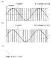
以下本発明のパラレル駆動バイアンプ切換回路の一実施形態例について、図面図1を参照しながら詳細に説明する。図1は本発明の一実施形態におけるのパラレル駆動バイアンプ切換回路のブロック図、図2は本発明の一実施形態において、CPUにより制御される各スイッチのオンオフ状態の組み合わせを示す説明図、図3は本発明の一実施形態におけるPWM信号と出力波形に対する発生ノイズ例を示す説明図である。 Hereinafter, an embodiment of a parallel drive bi-amp switching circuit according to the present invention will be described in detail with reference to FIG. FIG. 1 is a block diagram of a parallel drive biamplifier switching circuit according to an embodiment of the present invention. FIG. 2 is an explanatory diagram illustrating combinations of on / off states of switches controlled by a CPU according to an embodiment of the present invention. These are explanatory drawings which show the example of the generated noise with respect to the PWM signal and output waveform in one Embodiment of this invention.
図1において、第1ないし第14のスイッチであるS1ないしS14は連動スイッチで同時にオンまたはオフになる様に構成されている。 In FIG. 1, the first to fourteenth switches S1 to S14 are configured to be simultaneously turned on or off by interlocking switches.
4チャンネルの音声情報でエンコードされた2チャンネル入力信号が入力端子1L、1Rに入力されるデコーダであるプロロジックデコード部デコーダ2は、第1ないし第4の信号源であるデコード出力端子3L,3C,3R,3Sを有し、それぞれLチャンネル、Cチャンネル、RチャンネルおよびSチャンネルの信号を出力する。デコードの方法は周知であるからここでは説明しない。
The prologic
本実施形態では図示の第1〜第4の増幅器4A〜4Dはパルスワイドモジュレーション(PWM)方式を用いるものとし、第1の増幅器であるLチャンネル用増幅器4Aは、入力がスイッチS11を介してデコード出力端子3Lに接続され、出力は第1のスピーカであるLチャンネル用のスピーカ5の端子に接続されると共にスイッチS1を介して第2の増幅器であるCチャンネル用増幅器4Bの出力に接続される。
In the present embodiment, the illustrated first to
第2の増幅器である増幅器4Bは、入力をスイッチS2を介してデコード出力端子3Cに接続され、出力はスイッチS1を介してスピーカ5の端子に接続されると共にスイッチS3を介して第2のスピーカである図示しないCチャンネルスピーカの端子に接続されている。
The
また増幅器4Aの入力にはデコード出力端子3LからスイッチS12を介してデコード出力端子3Lとの間に第1の遅延回路8Lが接続されている。
The
更に増幅器4Bの入力にはスイッチS5を介してデコード出力端子3LにがスイッチS5を介して接続されている。
Further, the input of the
第3の増幅器であるRチャンネル用増幅器4Cは、入力がスイッチS13を介してデコード出力端子3Rに接続され、出力は第2のスピーカであるRチャンネル用のスピーカ6の端子に接続されると共にスイッチS6を介して第4の増幅器であるPWM方式のSチャンネル用増幅器4Dの出力に接続される。
The R-
第4の増幅器である増幅器4Dは、入力をスイッチS7を介してデコード出力端子3Sに接続され、出力はスイッチS6を介してスピーカ6の端子に接続されると共にスイッチS9を介して第4のスピーカである図示しないSチャンネルスピーカの端子に接続されている。
The
また増幅器4Cの入力にはスイッチS14を介してデコード出力端子3Rとの間に第2の遅延回路8Rが接続されている。
The
更に増幅器4Dの入力にはスイッチS10を介してデコード出力端子3Rに接続されている。以下RチャンネルとSチャンネルについても上記と同様である。
Further, the input of the
以上の様に構成されたパラレル駆動バイアンプ切換回路について、以下その動作を説明する。まずホーム・シアター再生機器として一般的である多チャンネル対応AVアンプとして用いる場合を説明する。チャンネル選択部105でが多チャンネル再生を選択した場合、映画等の多チャンネルエンコードされたソースは入力端子1L,1Rから入力され、プロロジックデコード部デコーダ2で4つの信号に分離され、出力端子3L,3C,3R,3Sに出力される。この時CPU101は、図2の4chに示すようにスイッチS2,S3,S7,S9,S11,S13をオンにし、スイッチS1,S5、S6,S10およびS12,S14をオフにする。プロロジックデコード部デコーダ2の出力端子3Lの出力はスイッチS5、S12が開いて、かつスイッチS11が閉じているので、増幅器4Aで増幅され、スイッチS1が開いている為Lチャンネル用スピーカ5の端子に印加されてノーマルモードで再生される。プロロジックデコード部デコーダ2の出力端子3Rの出力はスイッチS10,S14が開いて、かつスイッチS13が閉じているので、増幅器4Cで増幅され、スイッチS6が開いている為Rチャンネル用スピーカ6の端子に印加されてノーマルモードで再生される。
The operation of the parallel drive bi-amplifier switching circuit configured as described above will be described below. First, the case of using as a multi-channel compatible AV amplifier, which is a general home theater playback device, will be described. When the
プロロジックデコード部デコーダ2の出力端子3Cの出力はスイッチS2が閉じられているので増幅器4Bで増幅され、スイッチS1は開いてかつスイッチS3が閉じているのでCチャンネルスピーカで再生され、同じく出力端子3Sの出力はスイッチS7が閉じられているので増幅器4Dで増幅され、スイッチS6が開いてかつスイッチS9が閉じているのでSチャンネルスピーカで再生される。スイッチS5,S10、S12,S14が開いている為に遅延回路8L,8Rは動作していない。
The output of the
つぎに通常のステレオ再生の場合を説明する。プロロジックデコード部デコーダ2から出力される信号はLチャンネルとRチャンネルのみである。Lチャンネルについて説明すると、チャンネル選択部105が2チャンネルステレオ再生を選択した場合、CPU101は、図2の2chに示すようにスイッチS1,S5、S12を閉じ、スイッチS2、S3,S11を開く。出力端子3Lの信号は、スイッチS12から遅延回路8Lを通ってスイッチS12から増幅器4Aで増幅されてLチャンネル用スピーカ5の端子にの出力へ接続される経路とスイッチS5から第2のLチャンネル用増幅器4Bで増幅されてスイッチS1を通ってLチャンネル用スピーカ5の端子にの出力端子へ接続される経路とに二分され、Lチャンネル用再生スピーカ5をパラレル駆動バイアンプ方式で駆動再生することとなる。この時、遅延回路8Lがないと、従来のAVアンプにおけるPWM信号と出力波形に対する発生ノイズ例を示す説明図の図5(c)のノイズ波形の実線と破線の和に示すように2つのアンプの発生するノイズのタイミングが一致してノイズレベルが高くなる。遅延回路8Lにより並列駆動する相互の増幅器の入力信号のタイミングを一致させずに入力する事により、図3に示すように無帰還フルデジタルアンプの場合に発生するノイズが図3(c)の実線と遅延された破線のように一方が遅延することにより重畳を抑え、かつ他方の増幅器の帰還回路による影響を受けずに直結出来る事を特徴とする。図3、図5とも、簡単に示すためノイズは一波形ずつについて示している。
Next, the case of normal stereo playback will be described. The signals output from the prologic
ここで、遅延回路8Lの遅延時間の設定は、サンプリング周波数Fsをたとえば48kHzとすれば、ここで使用しているPWMモジュレータは1/4波長に対して256分割設定できる仕様のものを使った場合、少なくとも1/4波長に対して±(1/256)だけずらせばよい。したがって時間としては少なくとも、
(1/48000)÷4×(2/256)=0.041μs
程度となる。この遅延時間は、上記の値を最低値として、パラレル鼓動した場合の回路での歪等の最適値を勘案して決定する.
この場合、多チャンネル再生時にはLチャンネル用増幅器となる増幅器4AとCチャンネル用増幅器となる増幅器4Bは、パラレルに接続されLチャンネルスピーカ5を低インピーダンスで駆動し、低域成分の音質向上に効果があるダンピングファクターを増加する効果が期待できる。
Here, the delay time of the
(1/48000) ÷ 4 × (2/256) = 0.041 μs
It will be about. This delay time is determined by taking into consideration the optimum value such as distortion in the circuit when parallel beats, with the above value as the minimum value.
In this case, during multi-channel reproduction, the
Rチャンネルに対しても同様に、スイッチS6,S10、S14を閉じ、スイッチS7,S9,S13を開いておく。出力端子3Rの信号は、スイッチS14から遅延回路8Rを通ってスイッチS14から増幅器4Cで増幅されてRチャンネル用スピーカ6の端子にの出力端子へ接続される経路と、スイッチS10から第4のRチャンネル用増幅器4Dで増幅されてスイッチS6を通ってRチャンネル用スピーカ6の端子にの出力用端子へ接続される経路とに二分され、Rチャンネル用パラレル駆動バイワイヤリング再生スピーカ6をパラレル駆動バイアンプ方式で駆動再生することとなる。この時もLチャンネルと同様に、遅延回路8Rにより並列駆動する相互の増幅器の入力信号のタイミングを一致させずに入力する事により、図3に示すように無帰還フルデジタルアンプの場合に発生するノイズが図3(c)の実線と破線のように一方が遅延することにより重畳を抑え、かつ他方の増幅器の帰還回路による影響を受けずに直結出来る。
Similarly, for the R channel, the switches S6, S10, and S14 are closed and the switches S7, S9, and S13 are opened. The signal from the
この場合も、多チャンネル再生時にはRチャンネル用増幅器となる増幅器4CとSチャンネル用増幅器となる増幅器4Dは、パラレルに接続されLチャンネルスピーカ5を低インピーダンスで駆動し、低域成分音質向上に効果があるダンピングファクターを増加する効果が期待できる。
Also in this case, the
なお、上記の説明ではオンまたはオフするスイッチを用いたが、スイッチS1とS3、スイッチS6とS9とをそれぞれ切換スイッチにし、スイッチS2,S5,S7,S10,S11,S12,S13,S14を廃止し、代わりに増幅器4A,4B,4C,4Dに入力切換スイッチを設ければスイッチの数を減らす事が出来る。
In the above description, a switch that is turned on or off is used. However, the switches S1 and S3 and the switches S6 and S9 are changed to the changeover switches, and the switches S2, S5, S7, S10, S11, S12, S13, and S14 are abolished. However, if an input changeover switch is provided in the
また、スイッチの位置は図示の位置に限定されず、信号の経路が、各増幅器、遅延回路およびスピーカの間で請求の範囲に示された接続状態に切り換わり得るものであればよいものである。 Further, the position of the switch is not limited to the position shown in the figure, and any signal path may be used as long as the path of the signal can be switched to the connection state shown in the claims among the amplifiers, the delay circuit, and the speaker. .
また、CPU101は、チャネル選択部105から与えられる選択情報に従って、スイッチS1〜S14のオンオフを制御する。このチャネル選択部105は、AVアンプの操作パネルに設けられ、ユーザーによって操作される。チャネル選択部105は、2チャネルステレオ再生モードか4チャネル再生モードかを選択する。ROM102は、CPU101のための動作プログラムを格納している。CPU101は、この動作プログラムに従って動作する。RAM103は、CPU101がプログラム動作を行うときに発生する種々の作業データを記憶するワーキングメモリとして機能する。
Further, the
さらに、ここでは2個のアンプのパラレル駆動を説明したが、3個以上のアンプのパラレル駆動としてもよい。その場合遅延回路はパラレル数−1個必要であり、スイッチも上記に準じて増設すればよい。 Furthermore, although the parallel drive of two amplifiers was demonstrated here, it is good also as a parallel drive of three or more amplifiers. In that case, the number of delay circuits is required to be -1 in parallel, and the switches may be added in accordance with the above.
以上の様に本実施形態によれば、簡単なスイッチの切換回路と遅延回路をAVアンプ本体に追加する事により、多チャンネル再生用の増幅器をステレオ再生時に有効に用いてステレオ再生時の音質改善を図る事が出来る。 As described above, according to the present embodiment, by adding a simple switch switching circuit and a delay circuit to the AV amplifier main body, the amplifier for multi-channel reproduction is effectively used during stereo reproduction, thereby improving sound quality during stereo reproduction. Can be planned.
本発明のパラレル駆動バイアンプ切換回路は、多チャンネル再生及び2チャンネルステレオ再生が出来るAVアンプやレシーバなどの音響装置での音質向上用途にも適用できる産業上の利用可能性高いものである。 The parallel drive bi-amp switching circuit of the present invention has high industrial applicability that can be applied to sound quality improvement applications in audio devices such as AV amplifiers and receivers capable of multi-channel playback and 2-channel stereo playback.
1L,1R 入力端子
2 プロロジックデコード部デコーダ
3L,3C,3R,3S 出力端子
4A 第1の増幅器
4B 第2の増幅器
4C 第3の増幅器
4D 第4の増幅器
5 Lチャンネル用スピーカ
6 Rチャンネル用スピーカ
8L,8R 遅延回路
S1〜S14 スイッチ
101 CPU
102 ROM
103 RAM
105 チャンネル選択部
1L,
102 ROM
103 RAM
105 Channel selector
Claims (4)
PWM方式の第1の増幅器と、
PWM方式の第2の増幅器と、
前記第1の増幅器に接続する第1のスピーカと、
前記第2の増幅器に接続する第2のスピーカと、
遅延回路とを備え、
多チャンネル再生の時は第1の信号源の信号を前記第1の増幅器で増幅して前記第1のスピーカの端子に出力し前記第2の信号源の信号を前記第2の増幅器で増幅して前記第2のスピーカの端子に出力し、
2チャンネルステレオ再生の時は第1の信号源の信号を前記遅延回路を介して前記第1の増幅器で増幅して前記第1のスピーカの端子に出力すると共に前記第1の信号源の信号を前記第2の増幅器で増幅して前記第1のスピーカの同一端子に同一入力信号のタイミングを一致させることなく出力するように構成した事を特徴とするパラレル駆動バイアンプ切換回路。 A parallel drive bi-amp switching circuit used for an AV amplifier capable of selectively switching between a multi-channel playback mode and a 2-channel stereo playback mode,
A PWM first amplifier;
A PWM second amplifier;
A first speaker connected to the first amplifier;
A second speaker connected to the second amplifier;
A delay circuit,
During multi-channel reproduction, the signal from the first signal source is amplified by the first amplifier and output to the terminal of the first speaker, and the signal from the second signal source is amplified by the second amplifier. Output to the terminal of the second speaker,
During two-channel stereo reproduction, the signal from the first signal source is amplified by the first amplifier via the delay circuit and output to the terminal of the first speaker, and the signal from the first signal source is output from the first speaker. A parallel drive biamplifier switching circuit configured to be amplified by the second amplifier and output to the same terminal of the first speaker without matching the timing of the same input signal.
入力端子を第1の信号源にスイッチを介して接続し出力端子を第1のスピーカの端子に接続するPWM方式の第1の増幅器と、
入力端子を第2の信号源にスイッチを介して接続し出力をスイッチを介して前記第1のスピーカの端子に接続するかまたはスイッチを介して第2のスピーカの端子に接続するPWM方式の第2の増幅器と、
前記第1の信号源と前記第1の増幅器の入力との間にスイッチを介して接続された遅延回路と、
前記第1の信号源と前記第2の増幅器の入力との間にスイッチを介して接続された信号経路とを備え、
前記各部に配置された複数のスイッチの切換によって、
多チャンネル再生の時は第1の信号源の信号を前記第1の増幅器で増幅して前記第1のスピーカの端子に出力し前記第2の信号源の信号を前記第2の増幅器で増幅して前記第2のスピーカの端子に出力し、
2チャンネルステレオ再生の時は第1の信号源の信号を前記遅延回路を介して前記第1の増幅器で増幅して前記第1のスピーカの端子に出力すると共に前記第1の信号源の信号を前記第2の増幅器で増幅して前記第1のスピーカの同一出力端子に同一入力信号のタイミングを一致させることなく出力するように構成した事を特徴とするパラレル駆動バイアンプ切換回路。 A parallel drive bi-amp switching circuit used for an AV amplifier capable of selectively switching between a multi-channel playback mode and a 2-channel stereo playback mode,
A PWM-type first amplifier having an input terminal connected to a first signal source via a switch and an output terminal connected to a terminal of a first speaker;
A PWM type first terminal in which an input terminal is connected to a second signal source via a switch and an output is connected to a terminal of the first speaker via a switch or to a terminal of the second speaker via a switch. Two amplifiers;
A delay circuit connected via a switch between the first signal source and the input of the first amplifier;
A signal path connected via a switch between the first signal source and the input of the second amplifier;
By switching a plurality of switches arranged in each part,
During multi-channel reproduction, the signal from the first signal source is amplified by the first amplifier and output to the terminal of the first speaker, and the signal from the second signal source is amplified by the second amplifier. Output to the terminal of the second speaker,
During two-channel stereo reproduction, the signal from the first signal source is amplified by the first amplifier via the delay circuit and output to the terminal of the first speaker, and the signal from the first signal source is output from the first speaker. A parallel drive biamplifier switching circuit configured to amplify by the second amplifier and output the same input signal to the same output terminal of the first speaker without matching the timing of the same input signal.
前記複数のスイッチのオン、オフを制御するコンピュータ装置と、
前記コンピュータ装置に指示を与えるモード選択部とをさらに備えた請求項1から3のいずれかに記載のパラレル駆動バイアンプ切換回路。 A decoder as the signal source;
A computer device for controlling on and off of the plurality of switches;
4. The parallel drive biamplifier switching circuit according to claim 1, further comprising a mode selection unit that gives an instruction to the computer device.
Priority Applications (4)
| Application Number | Priority Date | Filing Date | Title |
|---|---|---|---|
| JP2005048351A JP4674474B2 (en) | 2005-02-24 | 2005-02-24 | Parallel drive bi-amp switching circuit |
| PCT/JP2006/303223 WO2006090758A1 (en) | 2005-02-24 | 2006-02-23 | A/v amplifier and method for driving the same |
| EP06714363.6A EP1853086B1 (en) | 2005-02-24 | 2006-02-23 | A/v amplifier and method for driving the same |
| US11/814,791 US8081781B2 (en) | 2005-02-24 | 2006-02-23 | A/V amplifier and method for driving the same |
Applications Claiming Priority (1)
| Application Number | Priority Date | Filing Date | Title |
|---|---|---|---|
| JP2005048351A JP4674474B2 (en) | 2005-02-24 | 2005-02-24 | Parallel drive bi-amp switching circuit |
Publications (3)
| Publication Number | Publication Date |
|---|---|
| JP2006237928A JP2006237928A (en) | 2006-09-07 |
| JP2006237928A5 JP2006237928A5 (en) | 2008-02-14 |
| JP4674474B2 true JP4674474B2 (en) | 2011-04-20 |
Family
ID=36927396
Family Applications (1)
| Application Number | Title | Priority Date | Filing Date |
|---|---|---|---|
| JP2005048351A Expired - Fee Related JP4674474B2 (en) | 2005-02-24 | 2005-02-24 | Parallel drive bi-amp switching circuit |
Country Status (4)
| Country | Link |
|---|---|
| US (1) | US8081781B2 (en) |
| EP (1) | EP1853086B1 (en) |
| JP (1) | JP4674474B2 (en) |
| WO (1) | WO2006090758A1 (en) |
Families Citing this family (19)
| Publication number | Priority date | Publication date | Assignee | Title |
|---|---|---|---|---|
| US20060262936A1 (en) * | 2005-05-13 | 2006-11-23 | Pioneer Corporation | Virtual surround decoder apparatus |
| JP4197040B2 (en) * | 2007-05-11 | 2008-12-17 | オンキヨー株式会社 | Multichannel amplifier |
| US8284963B2 (en) * | 2007-09-11 | 2012-10-09 | Texas Instruments Incorporated | Method and apparatus for diminishing mismatch effects between switched signals |
| JP4949193B2 (en) * | 2007-10-23 | 2012-06-06 | ティーオーエー株式会社 | Audio power amplifier |
| TW201019746A (en) * | 2008-11-05 | 2010-05-16 | Anpec Electronics Corp | Multi-channel output device for a multimedia device |
| JP4471030B1 (en) | 2009-02-03 | 2010-06-02 | オンキヨー株式会社 | Audio processing device |
| US8494183B2 (en) | 2009-02-03 | 2013-07-23 | Onkyo Corporation | Audio processing apparatus |
| US9426574B2 (en) | 2010-03-19 | 2016-08-23 | Bose Corporation | Automatic audio source switching |
| JP4997659B2 (en) | 2010-04-02 | 2012-08-08 | オンキヨー株式会社 | Audio processing device |
| JP5444173B2 (en) * | 2010-09-08 | 2014-03-19 | 株式会社東芝 | Amplifier and amplifier control method |
| US9543913B2 (en) | 2013-01-09 | 2017-01-10 | Osc, Llc | Programmably configured switchmode audio amplifier |
| US9984583B2 (en) * | 2013-09-20 | 2018-05-29 | Bose Corporation | Audio demonstration kit |
| US10134295B2 (en) | 2013-09-20 | 2018-11-20 | Bose Corporation | Audio demonstration kit |
| CN103702172A (en) * | 2013-12-13 | 2014-04-02 | 乐视网信息技术(北京)股份有限公司 | Method and system for carrying out dolby transcoding on AV (Audio/Video) |
| TWI583206B (en) * | 2015-07-15 | 2017-05-11 | 盛微先進科技股份有限公司 | Apparatus and method of stereo signals driving |
| WO2017164286A1 (en) * | 2016-03-23 | 2017-09-28 | ヤマハ株式会社 | Acoustic device setting method and acoustic device |
| US10901809B2 (en) | 2018-01-16 | 2021-01-26 | Qsc, Llc | Audio, video and control system implementing virtual machines |
| US11561813B2 (en) | 2018-01-16 | 2023-01-24 | Qsc, Llc | Server support for multiple audio/video operating systems |
| EP3756275A2 (en) | 2018-02-23 | 2020-12-30 | Qsc, Llc | Audio amplifier assemblies, processes, and methods |
Citations (4)
| Publication number | Priority date | Publication date | Assignee | Title |
|---|---|---|---|---|
| JPS6047316U (en) * | 1983-09-09 | 1985-04-03 | 日本コロムビア株式会社 | Amplifier |
| JPS60192512A (en) * | 1984-03-13 | 1985-10-01 | 井関農機株式会社 | Combine seeder |
| JPH09271100A (en) * | 1996-04-02 | 1997-10-14 | Nippon Columbia Co Ltd | Acoustic signal processing unit |
| JP2004048333A (en) * | 2002-07-11 | 2004-02-12 | Victor Co Of Japan Ltd | Pwm modulation class d amplifier |
Family Cites Families (8)
| Publication number | Priority date | Publication date | Assignee | Title |
|---|---|---|---|---|
| NL8105371A (en) | 1981-11-27 | 1983-06-16 | Philips Nv | DEVICE FOR CONTROLLING ONE OR MORE TURNOVER UNITS. |
| JPS6047316A (en) | 1983-08-23 | 1985-03-14 | 三菱電機株式会社 | Buffer gas breaker |
| JPS60192512U (en) * | 1984-05-30 | 1985-12-20 | 日本コロムビア株式会社 | power amplifier |
| JPH0623119Y2 (en) | 1989-01-24 | 1994-06-15 | パイオニア株式会社 | Surround stereo playback device |
| JPH0751169B2 (en) | 1993-04-22 | 1995-06-05 | 株式会社三共 | Pachinko machine |
| EP0866638B1 (en) | 1997-03-10 | 2011-06-15 | Panasonic Corporation | Audiovisual amplifier |
| US5875250A (en) * | 1998-02-02 | 1999-02-23 | Kuo; Mark | Single package three channel audio signal amplifier |
| JP2006033499A (en) * | 2004-07-16 | 2006-02-02 | Sony Corp | Class d amplifier |
-
2005
- 2005-02-24 JP JP2005048351A patent/JP4674474B2/en not_active Expired - Fee Related
-
2006
- 2006-02-23 EP EP06714363.6A patent/EP1853086B1/en not_active Expired - Fee Related
- 2006-02-23 WO PCT/JP2006/303223 patent/WO2006090758A1/en active Application Filing
- 2006-02-23 US US11/814,791 patent/US8081781B2/en not_active Expired - Fee Related
Patent Citations (4)
| Publication number | Priority date | Publication date | Assignee | Title |
|---|---|---|---|---|
| JPS6047316U (en) * | 1983-09-09 | 1985-04-03 | 日本コロムビア株式会社 | Amplifier |
| JPS60192512A (en) * | 1984-03-13 | 1985-10-01 | 井関農機株式会社 | Combine seeder |
| JPH09271100A (en) * | 1996-04-02 | 1997-10-14 | Nippon Columbia Co Ltd | Acoustic signal processing unit |
| JP2004048333A (en) * | 2002-07-11 | 2004-02-12 | Victor Co Of Japan Ltd | Pwm modulation class d amplifier |
Also Published As
| Publication number | Publication date |
|---|---|
| EP1853086A4 (en) | 2011-04-06 |
| WO2006090758A1 (en) | 2006-08-31 |
| US20090016539A1 (en) | 2009-01-15 |
| EP1853086A1 (en) | 2007-11-07 |
| US8081781B2 (en) | 2011-12-20 |
| JP2006237928A (en) | 2006-09-07 |
| EP1853086B1 (en) | 2018-04-04 |
Similar Documents
| Publication | Publication Date | Title |
|---|---|---|
| JP4674474B2 (en) | Parallel drive bi-amp switching circuit | |
| US4953213A (en) | Surround mode stereophonic reproducing equipment | |
| KR100682490B1 (en) | Audio signal processor and audio device | |
| JP2006148888A (en) | Method and apparatus to automatically set multi-channel speaker modes | |
| JPH11176101A (en) | Pseudo-multichannel stereo reproducing device | |
| JP3436681B2 (en) | AV amplifier | |
| JP2006050195A (en) | Av amplifier | |
| JP5892043B2 (en) | Audio processing device | |
| US5123051A (en) | Sound field reproducing apparatus | |
| JP2005184149A (en) | Sound reproducing system | |
| JP2007214726A (en) | Audio signal output apparatus and sound leakage reducing method | |
| JP2003274497A (en) | Multi-channel audio reproducing apparatus | |
| JP2002345100A (en) | Av amplifier and channel setting method of output terminal of the av amplifier | |
| JP4352176B2 (en) | Multi-channel reproduction system, sound source device used therefor, and amplification device | |
| JP2002027600A (en) | Multi-channel audio reproducing system | |
| JP3559838B2 (en) | Audio equipment | |
| JP2006101081A (en) | Acoustic reproduction device | |
| JP2003319487A (en) | Acoustic sound reproducer | |
| CA1321756C (en) | Sound field reproducing apparatus | |
| JP3788081B2 (en) | Sound equipment | |
| KR100677211B1 (en) | Car audio system capable of outputting separately various audio signals to speaker | |
| US20070073427A1 (en) | Audio signal processing device | |
| JP2000224699A (en) | Recording medium recording sound image localization processing program | |
| JPH10191203A (en) | Sound reproduction circuit | |
| JP2002112382A (en) | Sound reproducing device |
Legal Events
| Date | Code | Title | Description |
|---|---|---|---|
| A521 | Request for written amendment filed |
Free format text: JAPANESE INTERMEDIATE CODE: A523 Effective date: 20071220 |
|
| A621 | Written request for application examination |
Free format text: JAPANESE INTERMEDIATE CODE: A621 Effective date: 20071220 |
|
| RD01 | Notification of change of attorney |
Free format text: JAPANESE INTERMEDIATE CODE: A7421 Effective date: 20080115 |
|
| RD01 | Notification of change of attorney |
Free format text: JAPANESE INTERMEDIATE CODE: A7421 Effective date: 20091120 |
|
| TRDD | Decision of grant or rejection written | ||
| A01 | Written decision to grant a patent or to grant a registration (utility model) |
Free format text: JAPANESE INTERMEDIATE CODE: A01 Effective date: 20101228 |
|
| A01 | Written decision to grant a patent or to grant a registration (utility model) |
Free format text: JAPANESE INTERMEDIATE CODE: A01 |
|
| A61 | First payment of annual fees (during grant procedure) |
Free format text: JAPANESE INTERMEDIATE CODE: A61 Effective date: 20110110 |
|
| FPAY | Renewal fee payment (event date is renewal date of database) |
Free format text: PAYMENT UNTIL: 20140204 Year of fee payment: 3 |
|
| R151 | Written notification of patent or utility model registration |
Ref document number: 4674474 Country of ref document: JP Free format text: JAPANESE INTERMEDIATE CODE: R151 |
|
| FPAY | Renewal fee payment (event date is renewal date of database) |
Free format text: PAYMENT UNTIL: 20140204 Year of fee payment: 3 |
|
| LAPS | Cancellation because of no payment of annual fees |