JP4673584B2 - Cache memory device, arithmetic processing device, and control method for cache memory device - Google Patents
Cache memory device, arithmetic processing device, and control method for cache memory device Download PDFInfo
- Publication number
- JP4673584B2 JP4673584B2 JP2004222401A JP2004222401A JP4673584B2 JP 4673584 B2 JP4673584 B2 JP 4673584B2 JP 2004222401 A JP2004222401 A JP 2004222401A JP 2004222401 A JP2004222401 A JP 2004222401A JP 4673584 B2 JP4673584 B2 JP 4673584B2
- Authority
- JP
- Japan
- Prior art keywords
- data
- cache
- primary cache
- tag
- primary
- Prior art date
- Legal status (The legal status is an assumption and is not a legal conclusion. Google has not performed a legal analysis and makes no representation as to the accuracy of the status listed.)
- Expired - Fee Related
Links
Images


Classifications
-
- G—PHYSICS
- G06—COMPUTING; CALCULATING OR COUNTING
- G06F—ELECTRIC DIGITAL DATA PROCESSING
- G06F12/00—Accessing, addressing or allocating within memory systems or architectures
- G06F12/02—Addressing or allocation; Relocation
- G06F12/08—Addressing or allocation; Relocation in hierarchically structured memory systems, e.g. virtual memory systems
- G06F12/10—Address translation
- G06F12/1027—Address translation using associative or pseudo-associative address translation means, e.g. translation look-aside buffer [TLB]
- G06F12/1045—Address translation using associative or pseudo-associative address translation means, e.g. translation look-aside buffer [TLB] associated with a data cache
-
- G—PHYSICS
- G06—COMPUTING; CALCULATING OR COUNTING
- G06F—ELECTRIC DIGITAL DATA PROCESSING
- G06F12/00—Accessing, addressing or allocating within memory systems or architectures
- G06F12/02—Addressing or allocation; Relocation
- G06F12/08—Addressing or allocation; Relocation in hierarchically structured memory systems, e.g. virtual memory systems
- G06F12/0802—Addressing of a memory level in which the access to the desired data or data block requires associative addressing means, e.g. caches
- G06F12/0893—Caches characterised by their organisation or structure
- G06F12/0897—Caches characterised by their organisation or structure with two or more cache hierarchy levels
Description
この発明は、キャッシュメモリ装置、演算処理装置及びキャッシュメモリ装置の制御方法に関するものである。 This invention relates to a control method of key Yasshumemori device, processing unit and the cache memory device.
近年、CPU(Central Processing Unit)およびメインメモリ間に発生するデータ遅延の問題を解消すべくキャッシュメモリが利用されている。このキャッシュメモリは、それ自体階層構造になっており、現在では複数のキャッシュメモリを用いている。そして、CPUに近い高速なキャッシュメモリから順に、第1レベルキャッシュおよび第2レベルキャッシュとして分類される。 In recent years, a cache memory has been used to solve the problem of data delay occurring between a CPU (Central Processing Unit) and a main memory. This cache memory itself has a hierarchical structure, and currently uses a plurality of cache memories. Then, the cache is classified into a first level cache and a second level cache in order from a high-speed cache memory close to the CPU.
また、従来に係るキャッシュメモリは、第1レベルキャッシュに対するタグの写しを、第2レベルキャッシュに保持させ、第2レベルキャッシュが該タグの写しを利用し、第1レベルキャッシュの情報を得ることによって、第1レベルキャッシュおよび第2レベルキャッシュ間の相互矛盾を無くしている。 Further, the cache memory according to the related art holds a copy of the tag for the first level cache in the second level cache, and the second level cache uses the copy of the tag to obtain information of the first level cache. The mutual contradiction between the first level cache and the second level cache is eliminated.
例えば、図11に示すように、物理インデックスで第2レベルキャッシュのタグにアクセスした場合に、第2レベルキャッシュに含まれる仮想インデックスを利用して第1レベルキャッシュのタグの写しにアクセスし、第1レベルキャッシュの登録状態を把握することによって、両者のコヒーレンシを維持している。 For example, as shown in FIG. 11, when the tag of the second level cache is accessed by the physical index, the copy of the tag of the first level cache is accessed using the virtual index included in the second level cache, By grasping the registration state of the one-level cache, the coherency of both is maintained.
なお、特許文献1では、キャッシュに含まれる各キャッシュラインに状態ビットフィールドなどを関連付けて、キャッシュライン状態のデコード効率を向上させる技術が公開されており、特許文献2では、共用の第2レベルキャッシュに包含ビット、命令ビットおよびデータビットを有するディレクトリを含ませることでデータキャッシュの包含を正確に追跡可能とする技術が公開されている。 Patent Document 1 discloses a technique for improving the decoding efficiency of a cache line state by associating a state bit field with each cache line included in the cache, and Patent Document 2 discloses a shared second level cache. A technology has been disclosed that allows the inclusion of a data cache to be accurately tracked by including a directory having inclusion bits, instruction bits, and data bits.
しかしながら、従来に係る技術では、キャッシュメモリのマシンサイクルを高速化することができないという問題があった。 However, the related art has a problem that the machine cycle of the cache memory cannot be increased.
具体的には、第2レベルキャッシュと第1レベルキャッシュとの間で相互矛盾を無くすために、第2レベルキャッシュが第1レベルキャッシュの登録情報を得る際、タグを2段階でアクセスするため、ディレイが発生してしまうからである。 Specifically, in order to eliminate mutual contradiction between the second level cache and the first level cache, when the second level cache obtains the registration information of the first level cache, the tag is accessed in two stages. This is because a delay occurs.
また、年々CPUの処理速度が飛躍的に向上しているが、CPUにデータを渡すキャッシュメモリの処理速度が遅いことは、CPUの足かせとなってしまうため、キャッシュメモリに発生するディレイの問題は更に深刻なものとなる。 Moreover, although the processing speed of the CPU has been dramatically improved year by year, the slow processing speed of the cache memory for passing data to the CPU is a drag on the CPU, so the problem of delay occurring in the cache memory is It becomes even more serious.
すなわち、第1レベルキャッシュの登録情報を得る際に発生するディレイをなくし、マシンサイクルを高速化させることが極めて重要な課題となっている。 In other words, it is an extremely important issue to eliminate the delay that occurs when obtaining the registration information of the first level cache and to speed up the machine cycle.
この発明は、上述した従来技術による問題点を解消するためになされたものであり、キャッシュメモリに発生するディレイをなくし、マシンサイクルを高速化することができるキャッシュメモリ装置、演算処理装置及びキャッシュメモリ装置の制御方法を提供することを目的とする。 The present invention has been made to solve the above-described problems caused by the prior art, and eliminates a delay that occurs in a cache memory, and can speed up a machine cycle, a cache memory device , an arithmetic processing unit, and a cache memory An object is to provide a method for controlling an apparatus .
上述した課題を解決し、目的を達成するため、本発明は、データを保持する1次キャッシュメモリと前記データを保持する2次キャッシュメモリを有し、演算処理部からのメモリアクセス要求に対応するデータを前記演算処理部に出力するキャッシュメモリ装置において、前記1次キャッシュメモリは、データを登録する1次キャッシュデータ部と、前記1次キャッシュデータ部が登録するデータについてのタグであって、第1の物理アドレスを含む1次キャッシュタグを保持する1次キャッシュタグ部と、前記演算処理部が出力したメモリアクセス要求に含まれ、1次キャッシュインデックスを含む仮想アドレスを、タグ比較アドレスと2次キャッシュインデックスとを含む物理アドレスに変換するアドレス変換処理部と、1次キャッシュインデックスを用いて前記1次キャッシュタグ部を検索し、前記検索された1次キャッシュタグが含む第1の物理アドレスとタグ比較アドレスを比較し、一致の場合には、前記第1の物理アドレスに対応する前記1次キャッシュデータ部が登録するデータを前記演算処理部に出力し、不一致の場合には、前記1次キャッシュインデックスと前記物理アドレスを出力する第1の検索処理部を有し、前記2次キャッシュメモリは、前記1次キャッシュデータ部が登録するデータを記憶する2次キャッシュデータ部と、前記2次キャッシュデータ部が保持するデータについてのタグであって、第2の物理アドレスと、仮想インデックスと、前記2次キャッシュデータ部が保持する前記1次キャッシュデータ部に登録されたデータについての登録情報である1次キャッシュ登録情報とを含む2次キャッシュタグを保持する2次キャッシュタグ部と、前記第1の検索処理部が出力した物理アドレスに含まれる2次キャッシュインデックスを用いて前記2次キャッシュタグ部を検索し、前記検索された2次キャッシュタグが含む第2の物理アドレスと前記第1の検索処理部が出力した物理アドレスに含まれるタグ比較アドレスを比較し、一致の場合には、前記第1の検索処理部が出力した前記1次キャッシュインデックスと検索された2次キャッシュタグが含む仮想インデックスをさらに比較し、前記1次キャッシュインデックスと前記仮想インデックスが一致する場合には、前記第2の物理アドレスに対応する前記2次キャッシュデータ部が保持するデータを前記1次キャッシュデータ部に登録するとともに前記演算処理部に出力し、前記1次キャッシュインデックスと前記仮想インデックスが一致しない場合には、前記検索された2次キャッシュタグが含む1次キャッシュ登録情報に基づき、前記仮想インデックスに対応するデータが前記1次キャッシュデータ部に登録され且つ前記2次キャッシュデータ部が保持する前記1次キャッシュデータ部に登録されたデータを前記演算処理部が書き換え得る更新型であると判断した場合には、前記仮想インデックスに対応する前記1次キャッシュデータデータ部から出力させたデータを前記2次キャッシュデータ部に保持させるコヒーレンシ維持部を有することを特徴とする。 In order to solve the above-described problems and achieve the object, the present invention has a primary cache memory that holds data and a secondary cache memory that holds the data, and responds to a memory access request from an arithmetic processing unit. In the cache memory device that outputs data to the arithmetic processing unit, the primary cache memory includes a primary cache data unit for registering data and a tag for data registered by the primary cache data unit, A primary cache tag unit that holds a primary cache tag including one physical address, a virtual address that is included in the memory access request output by the arithmetic processing unit and includes a primary cache index, and a tag comparison address and a secondary address Address conversion processing unit for converting to a physical address including a cache index and a primary cache The primary cache tag portion is searched using an index, the first physical address included in the searched primary cache tag is compared with the tag comparison address, and if they match, the first physical address is set to the first physical address. A first search processing unit that outputs the data registered in the corresponding primary cache data unit to the arithmetic processing unit, and outputs the primary cache index and the physical address if they do not match; The secondary cache memory is a tag for data stored in the secondary cache data part, a secondary cache data part for storing data registered by the primary cache data part, a second physical address, Registration information about virtual index and data registered in the primary cache data part held by the secondary cache data part A secondary cache tag unit that holds a secondary cache tag including certain primary cache registration information, and the secondary cache tag using a secondary cache index included in a physical address output by the first search processing unit A second physical address included in the retrieved secondary cache tag is compared with a tag comparison address included in the physical address output by the first search processing unit. The primary cache index output from the first search processing unit is further compared with the virtual index included in the searched secondary cache tag, and when the primary cache index and the virtual index match, The data held in the secondary cache data part corresponding to the physical address of is registered in the primary cache data part If the primary cache index and the virtual index do not match, the virtual cache corresponds to the virtual index based on the primary cache registration information included in the searched secondary cache tag. When it is determined that the data is registered in the primary cache data part and the arithmetic processing unit can rewrite the data registered in the primary cache data part held by the secondary cache data part. And a coherency maintaining unit for holding data output from the primary cache data data unit corresponding to the virtual index in the secondary cache data unit.
また、本発明は、前記キャッシュメモリ装置において、前記コヒーレンシ維持部はさらに、前記1次キャッシュインデックスと前記仮想インデックスが一致しない場合であって、前記検索された2次キャッシュタグが含む1次キャッシュ登録情報に基づき、前記仮想インデックスに対応するデータが前記1次キャッシュデータ部に登録され且つ前記更新型でないと判断した場合には、前記仮想インデックスに対応する前記1次キャッシュデータ部が登録するデータを無効化することを特徴とする。 In the cache memory device, the coherency maintenance unit may further include a primary cache registration included in the searched secondary cache tag when the primary cache index does not match the virtual index. Based on the information, if it is determined that the data corresponding to the virtual index is registered in the primary cache data portion and is not the update type, the data registered by the primary cache data portion corresponding to the virtual index is It is characterized by invalidation.
また、本発明は、前記キャッシュメモリ装置において、前記コヒーレンシ維持部はさらに、前記1次キャッシュインデックスと前記仮想インデックスが一致しない場合であって、前記検索された2次キャッシュタグが含む1次キャッシュ登録情報に基づき、前記仮想インデックスに対応するデータが前記1次キャッシュデータ部に登録されていないと判断した場合には、前記第2の物理アドレスに対応する前記2次キャッシュデータ部が保持するデータを前記1次キャッシュデータ部に登録することを特徴とする。 In the cache memory device, the coherency maintenance unit may further include a primary cache registration included in the searched secondary cache tag when the primary cache index does not match the virtual index. If it is determined that the data corresponding to the virtual index is not registered in the primary cache data part based on the information, the data held by the secondary cache data part corresponding to the second physical address is stored. It is registered in the primary cache data part.
また、本発明は、前記キャッシュメモリ装置において、前記2次キャッシュメモリ部は複数のウェイを有し、前記1次キャッシュタグはさらに、前記1次キャッシュメモリ部が登録するデータが前記2次キャッシュメモリ部のどのウェイに登録されているかを示すウェイ特定情報を含み、前記1次キャッシュメモリはさらに、検出した前記1次キャッシュデータ部又は前記1次キャッシュタグ部にエラーが発生した旨と、前記エラーが発生したデータに対応する1次キャッシュタグに含まれる1次キャッシュインデックスと前記エラーが発生したウェイを特定するエラーウェイ特定情報を前記2次キャッシュメモリに通知するエラー検出部を有し、前記2次キャッシュメモリはさらに、前記エラー検出部が通知した1次キャッシュインデックスを用いて前記2次キャッシュタグ部を検索し、前記1次キャッシュインデックスと等しい仮想インデックスを含む2次キャッシュタグが検索された場合、前記検索された2次キャッシュタグが含む1次キャッシュ登録情報が含むウェイ特定情報と前記エラー検出部が通知したエラーウェイ特定情報を比較し、一致の場合には、前記検索された2次キャッシュタグが含む1次キャッシュ登録情報に基づき、前記仮想インデックスに対応するデータが前記1次キャッシュデータ部に登録され且つ更新型であると判断した場合には、前記1次キャッシュデータ部から出力させた前記仮想インデックスに対応するデータを前記2次キャッシュデータ部に保持させるエラー処理部を有することを特徴とする。 In the cache memory device according to the present invention, the secondary cache memory unit includes a plurality of ways, and the primary cache tag further includes data registered by the primary cache memory unit as the secondary cache memory. Including the way identification information indicating which way of the unit is registered, the primary cache memory further indicating that an error has occurred in the detected primary cache data unit or the primary cache tag unit, and the error An error detection unit for notifying the secondary cache memory of a primary cache index included in a primary cache tag corresponding to the data in which the error has occurred and error way specifying information for specifying the way in which the error has occurred; The next cache memory further includes a first cache index notified by the error detection unit. When the secondary cache tag portion is searched using a search, and a secondary cache tag including a virtual index equal to the primary cache index is searched, primary cache registration information included in the searched secondary cache tag is The way specification information included is compared with the error way specification information notified by the error detection unit. If they match, the virtual index is determined based on the primary cache registration information included in the searched secondary cache tag. When it is determined that the data is registered in the primary cache data part and is an update type, the data corresponding to the virtual index output from the primary cache data part is held in the secondary cache data part It has an error processing part.
また、本発明は、前記キャッシュメモリ装置において、前記エラー処理部は、前記検索された2次キャッシュタグが含む1次キャッシュ登録情報に基づき、前記仮想インデックスに対応するデータが前記1次キャッシュデータ部に登録され且つ前記更新型でないと判断した場合には、前記仮想インデックスに対応する前記1次キャッシュデータ部が登録するデータを無効化することを特徴とする。 Further, the present invention is the cache memory device, wherein the error processing unit is configured such that data corresponding to the virtual index is based on the primary cache registration information included in the searched secondary cache tag. When it is determined that the update type is not registered, the data registered by the primary cache data unit corresponding to the virtual index is invalidated.
また、本発明は、前記キャッシュメモリ装置において、前記エラー処理部は、前記検索された2次キャッシュタグが含む1次キャッシュ登録情報が含むウェイ特定情報と前記エラー検出部が通知したエラーウェイ特定情報を比較し、全てのタグが不一致の場合には、前記1次キャッシュインデックスに対応する前記1次キャッシュデータ部が登録するデータと前記エラー検出部が通知したエラーウェイ特定情報に対応する前記2次キャッシュデータ部のウェイに保持されるデータを無効化することを特徴とする。 Further, the present invention is the cache memory device, wherein the error processing unit includes way specification information included in primary cache registration information included in the searched secondary cache tag and error way specification information notified by the error detection unit. If all the tags do not match, the data registered in the primary cache data part corresponding to the primary cache index and the secondary corresponding to the error way specifying information notified by the error detection part The data stored in the way of the cache data part is invalidated.
また、本発明は、メモリアクセス要求を出力する演算処理部と、データを保持する1次キャッシュメモリと前記データを保持する2次キャッシュメモリを有し、前記メモリアクセス要求に対応するデータを前記演算処理部に出力するキャッシュメモリ部とを有する演算処理装置において、前記1次キャッシュメモリは、データを登録する1次キャッシュデータ部と、前記1次キャッシュデータ部が登録するデータについてのタグであって、第1の物理アドレスを含む1次キャッシュタグを保持する1次キャッシュタグ部と、前記演算処理部が出力したメモリアクセス要求に含まれ、1次キャッシュインデックスを含む仮想アドレスを、タグ比較アドレスと2次キャッシュインデックスとを含む物理アドレスに変換するアドレス変換処理部と、1次キャッシュインデックスを用いて前記1次キャッシュタグ部を検索し、前記検索された1次キャッシュタグが含む第1の物理アドレスとタグ比較アドレスを比較し、一致の場合には、前記第1の物理アドレスに対応する前記1次キャッシュデータ部が登録するデータを前記演算処理部に出力し、不一致の場合には、前記1次キャッシュインデックスと前記物理アドレスを出力する第1の検索処理部を有し、前記2次キャッシュメモリは、前記1次キャッシュデータ部が登録するデータを記憶する2次キャッシュデータ部と、前記2次キャッシュデータ部が保持するデータについてのタグであって、第2の物理アドレスと、仮想インデックスと、前記2次キャッシュデータ部が保持する前記1次キャッシュデータ部に登録されたデータについての登録情報である1次キャッシュ登録情報とを含む2次キャッシュタグを保持する2次キャッシュタグ部と、前記第1の検索処理部が出力した物理アドレスに含まれる2次キャッシュインデックスを用いて前記2次キャッシュタグ部を検索し、前記検索された2次キャッシュタグが含む第2の物理アドレスと前記第1の検索処理部が出力した物理アドレスに含まれるタグ比較アドレスを比較し、一致の場合には、前記第1の検索処理部が出力した前記1次キャッシュインデックスと検索された2次キャッシュタグが含む仮想インデックスをさらに比較し、前記1次キャッシュインデックスと前記仮想インデックスが一致する場合には、前記第2の物理アドレスに対応する前記2次キャッシュデータ部が保持するデータを前記1次キャッシュデータ部に登録するとともに前記演算処理部に出力し、前記1次キャッシュインデックスと前記仮想インデックスが一致しない場合には、前記検索された2次キャッシュタグが含む1次キャッシュ登録情報に基づき、前記仮想インデックスに対応するデータが前記1次キャッシュデータ部に登録され且つ前記2次キャッシュデータ部が保持する前記1次キャッシュデータ部に登録されたデータを前記演算処理部が書き換え得る更新型であると判断した場合には、前記仮想インデックスに対応する前記1次キャッシュデータデータ部から出力させたデータを前記2次キャッシュデータ部に保持させるコヒーレンシ維持部を有することを特徴とする。 The present invention further includes an arithmetic processing unit that outputs a memory access request, a primary cache memory that stores data, and a secondary cache memory that stores the data, and the data corresponding to the memory access request is processed by the arithmetic operation unit. In the arithmetic processing unit having a cache memory unit for outputting to a processing unit, the primary cache memory is a tag for a primary cache data unit for registering data and data registered by the primary cache data unit. , A primary cache tag unit that holds a primary cache tag including a first physical address, and a virtual address that is included in the memory access request output by the arithmetic processing unit and includes a primary cache index is a tag comparison address An address conversion processing unit for converting into a physical address including a secondary cache index; The primary cache tag portion is searched using a next cache index, the first physical address included in the searched primary cache tag is compared with the tag comparison address, and if they match, the first physical address is compared. A first search processing unit that outputs data registered in the primary cache data unit corresponding to an address to the arithmetic processing unit, and outputs the primary cache index and the physical address if they do not match; The secondary cache memory is a tag for a secondary cache data part for storing data registered by the primary cache data part and data held by the secondary cache data part, and a second physical address And the virtual index and the data registered in the primary cache data part held by the secondary cache data part. Using a secondary cache tag part that holds a secondary cache tag including primary cache registration information that is all registration information, and a secondary cache index contained in the physical address output by the first search processing part The secondary cache tag part is searched, a second physical address included in the searched secondary cache tag is compared with a tag comparison address included in the physical address output by the first search processing part, and a match is found. In this case, the primary cache index output from the first search processing unit is further compared with the virtual index included in the searched secondary cache tag, and the primary cache index and the virtual index match. The data stored in the secondary cache data portion corresponding to the second physical address is transferred to the primary cache. When the primary cache index and the virtual index do not match, the virtual part is registered based on the primary cache registration information included in the searched secondary cache tag. It is determined that the data corresponding to the index is registered in the primary cache data part and that the arithmetic processing unit can rewrite the data registered in the primary cache data part held by the secondary cache data part. In such a case, a coherency maintenance unit is provided that causes the secondary cache data unit to hold data output from the primary cache data data unit corresponding to the virtual index.
また、本発明は、前記演算処理装置において、前記コヒーレンシ維持部はさらに、前記1次キャッシュインデックスと前記仮想インデックスが一致しない場合であって、前記検索された2次キャッシュタグが含む1次キャッシュ登録情報に基づき、前記仮想インデックスに対応するデータが前記1次キャッシュデータ部に登録され且つ前記更新型でないと判断した場合には、前記仮想インデックスに対応する前記1次キャッシュデータ部が登録するデータを無効化することを特徴とする。 In the arithmetic processing unit according to the present invention , the coherency maintaining unit may further include a primary cache registration included in the searched secondary cache tag when the primary cache index does not match the virtual index. Based on the information, if it is determined that the data corresponding to the virtual index is registered in the primary cache data portion and is not the update type, the data registered by the primary cache data portion corresponding to the virtual index is It is characterized by invalidation.
また、本発明は、前記演算処理装置において、前記コヒーレンシ維持部はさらに、前記1次キャッシュインデックスと前記仮想インデックスが一致しない場合であって、前記検索された2次キャッシュタグが含む1次キャッシュ登録情報に基づき、前記仮想インデックスに対応するデータが前記1次キャッシュデータ部に登録されていないと判断した場合には、前記第2の物理アドレスに対応する前記2次キャッシュデータ部が保持するデータを前記1次キャッシュデータ部に登録することを特徴とする。 In the arithmetic processing unit according to the present invention , the coherency maintaining unit may further include a primary cache registration included in the searched secondary cache tag when the primary cache index does not match the virtual index. If it is determined that the data corresponding to the virtual index is not registered in the primary cache data part based on the information, the data held by the secondary cache data part corresponding to the second physical address is stored. It is registered in the primary cache data part.
また、本発明は、前記演算処理装置において、前記2次キャッシュメモリ部は複数のウェイを有し、前記1次キャッシュタグはさらに、前記1次キャッシュメモリ部が登録するデータが前記2次キャッシュメモリ部のどのウェイに登録されているかを示すウェイ特定情報を含み、前記1次キャッシュメモリはさらに、検出した前記1次キャッシュデータ部又は前記1次キャッシュタグ部にエラーが発生した旨と、前記エラーが発生したデータに対応する1次キャッシュタグに含まれる1次キャッシュインデックスと前記エラーが発生したウェイを特定するエラーウェイ特定情報を前記2次キャッシュメモリに通知するエラー検出部を有し、前記2次キャッシュメモリはさらに、前記エラー検出部が通知した1次キャッシュインデックスを用いて前記2次キャッシュタグ部を検索し、前記1次キャッシュインデックスと等しい仮想インデックスを含む2次キャッシュタグが検索された場合、前記検索された2次キャッシュタグが含む1次キャッシュ登録情報が含むウェイ特定情報と前記エラー検出部が通知したエラーウェイ特定情報を比較し、一致の場合には、前記検索された2次キャッシュタグが含む1次キャッシュ登録情報に基づき、前記仮想インデックスに対応するデータが前記1次キャッシュデータ部に登録され且つ更新型であると判断した場合には、前記1次キャッシュデータ部から出力させた前記仮想インデックスに対応するデータを前記2次キャッシュデータ部に保持させるエラー処理部を有することを特徴とする。
また、本発明は、前記演算処理装置において、前記エラー処理部は、前記検索された2次キャッシュタグが含む1次キャッシュ登録情報に基づき、前記仮想インデックスに対応するデータが前記1次キャッシュデータ部に登録され且つ前記更新型でないと判断した場合には、前記仮想インデックスに対応する前記1次キャッシュデータ部が登録するデータを無効化することを特徴とする。
また、本発明は、前記演算処理装置において、前記エラー処理部は、前記検索された2次キャッシュタグが含む1次キャッシュ登録情報が含むウェイ特定情報と前記エラー検出部が通知したエラーウェイ特定情報を比較し、全てのタグが不一致の場合には、前記1次キャッシュインデックスに対応する前記1次キャッシュデータ部が登録するデータと前記エラー検出部が通知したエラーウェイ特定情報に対応する前記2次キャッシュデータ部のウェイに保持されるデータを無効化することを特徴とする。
また、本発明は、データを登録する1次キャッシュデータ部と、前記1次キャッシュデータ部が登録するデータについてのタグであって、第1の物理アドレスを含む1次キャッシュタグを保持する1次キャッシュタグ部を備えた1次キャッシュメモリと、前記1次キャッシュデータ部が登録するデータを記憶する2次キャッシュデータ部と、前記2次キャッシュデータ部が保持するデータについてのタグであって、第2の物理アドレスと、仮想インデックスと、前記2次キャッシュデータ部が保持する前記1次キャッシュデータ部に登録されたデータについての登録情報である1次キャッシュ登録部とを含む2次キャッシュタグを保持する2次キャッシュタグ部を備えた2次キャッシュメモリを有し、演算処理部からのメモリアクセス要求に対応するデータを前記演算処理部に出力するキャッシュメモリ装置の制御方法において、前記1次キャッシュメモリが有するアドレス変換処理部が、前記演算処理部が出力したメモリアクセス要求に含まれ、1次キャッシュインデックスを含む仮想アドレスを、タグ比較アドレスと2次キャッシュインデックスとを含む物理アドレスに変換するステップと、前記1次キャッシュメモリが有する第1の検索処理部が、1次キャッシュインデックスを用いて前記1次キャッシュタグ部を検索し、前記検索された1次キャッシュタグが含む第1の物理アドレスとタグ比較アドレスを比較し、一致の場合には、前記第1の物理アドレスに対応する前記1次キャッシュデータ部が登録するデータを前記演算処理部に出力し、不一致の場合には、前記1次キャッシュインデックスと前記物理アドレスを出力するステップと、前記2次キャッシュメモリが有するコヒーレンシ維持部が、前記第1の検索処理部が出力した物理アドレスに含まれる2次キャッシュインデックスを用いて前記2次キャッシュタグ部を検索するステップと、前記コヒーレンシ維持部が、前記検索された2次キャッシュタグが含む第2の物理アドレスと前記第1の検索処理部が出力した物理アドレスに含まれるタグ比較アドレスを比較するステップと、前記比較の結果、一致の場合には、前記コヒーレンシ維持部が、前記第1の検索処理部が出力した前記1次キャッシュインデックスと検索された2次キャッシュタグが含む仮想インデックスが一致する場合には、前記第2の物理アドレスに対応する前記2次キャッシュデータ部が保持するデータを前記1次キャッシュデータ部に登録するとともに前記演算処理部に出力し、前記1次キャッシュインデックスと前記仮想インデックスが一致しない場合には、前記検索された2次キャッシュタグが含む1次キャッシュ登録情報に基づき、前記仮想インデックスに対応するデータが前記1次キャッシュデータ部に登録され且つ前記2次キャッシュデータ部が保持する前記1次キャッシュデータ部に登録されたデータを前記演算処理部が書き換え得る更新型であると判断した場合には、前記仮想インデックスに対応する前記1次キャッシュデータ部から出力させたデータを前記2次キャッシュデータ部に保持させるステップを有することを特徴とする。
In the arithmetic processing unit according to the present invention, the secondary cache memory unit includes a plurality of ways, and the primary cache tag further includes data registered by the primary cache memory unit as the secondary cache memory. Including the way identification information indicating which way of the unit is registered, the primary cache memory further indicating that an error has occurred in the detected primary cache data unit or the primary cache tag unit, and the error An error detection unit for notifying the secondary cache memory of a primary cache index included in a primary cache tag corresponding to the data in which the error has occurred and error way specifying information for specifying the way in which the error has occurred; The next cache memory further uses the first cache index notified by the error detection unit. When the secondary cache tag portion is searched and a secondary cache tag including a virtual index equal to the primary cache index is searched, the way identification included in the primary cache registration information included in the searched secondary cache tag The information and the error way identification information notified by the error detection unit are compared, and if they match, the data corresponding to the virtual index is based on the primary cache registration information included in the searched secondary cache tag. An error processing unit that stores data corresponding to the virtual index output from the primary cache data unit in the secondary cache data unit when it is determined to be registered and updated in the primary cache data unit It is characterized by having.
Further, the present invention is the arithmetic processing unit, wherein the error processing unit is configured such that the data corresponding to the virtual index is based on the primary cache registration information included in the searched secondary cache tag. When it is determined that the update type is not registered, the data registered by the primary cache data unit corresponding to the virtual index is invalidated.
Also, in the arithmetic processing unit according to the present invention, the error processing unit includes way specification information included in primary cache registration information included in the searched secondary cache tag and error way specification information notified by the error detection unit. If all the tags do not match, the data registered in the primary cache data part corresponding to the primary cache index and the secondary corresponding to the error way specifying information notified by the error detection part The data stored in the way of the cache data part is invalidated.
The present invention also provides a primary cache data part for registering data and a tag for data registered by the primary cache data part, the primary cache data holding a primary cache tag including a first physical address. A primary cache memory having a cache tag part, a secondary cache data part for storing data registered by the primary cache data part, and a tag for data held by the secondary cache data part, 2 holds a secondary cache tag including a physical address, a virtual index, and a primary cache registration unit that is registration information about data registered in the primary cache data unit held by the secondary cache data unit. A secondary cache memory having a secondary cache tag unit for performing a memory access request from the arithmetic processing unit In the control method of the cache memory device for outputting the corresponding data to the arithmetic processing unit, the address conversion processing unit included in the primary cache memory is included in the memory access request output from the arithmetic processing unit, and the primary cache index A virtual address including a tag comparison address and a physical address including a secondary cache index, and a first search processing unit included in the primary cache memory uses the primary cache index to convert the primary address A cache tag part is searched, a first physical address included in the searched primary cache tag is compared with a tag comparison address, and if they match, the primary cache data corresponding to the first physical address is compared. The data registered by the unit is output to the arithmetic processing unit. A step of outputting a cache index and the physical address, and a coherency maintaining unit included in the secondary cache memory using the secondary cache index included in the physical address output by the first search processing unit. A step of searching for a next cache tag part; and a tag comparison address included in the second physical address included in the searched secondary cache tag by the coherency maintaining part and the physical address output by the first search processing part. And if the result of the comparison is a match, the coherency maintaining unit includes a virtual index included in the searched secondary cache tag and the primary cache index output from the first search processing unit. If the two match, the secondary cache data corresponding to the second physical address Data stored in the primary cache data unit and output to the arithmetic processing unit, and if the primary cache index and the virtual index do not match, the retrieved secondary cache tag includes Based on the primary cache registration information, the data corresponding to the virtual index is registered in the primary cache data part and the data registered in the primary cache data part held by the secondary cache data part is subjected to the arithmetic processing. And when the second cache data part holds the data output from the primary cache data part corresponding to the virtual index when it is determined that the part is an rewritable update type. .
本発明によれば、第1レベルキャッシュメモリ部に係る情報の一部を記憶させ、該第1レベルキャッシュメモリ部に係る情報の一部を基にして、第1レベルキャッシュメモリ部と第2レベルキャッシュメモリ部との間で、コヒーレンシを維持するので、迅速に第1レベルキャッシュメモリ部の登録状態を把握でき、マシンサイクルを高速化することができるという効果を奏する。 According to the present invention, a part of the information related to the first level cache memory unit is stored, and the first level cache memory unit and the second level based on the part of the information related to the first level cache memory unit are stored. Since coherency is maintained with the cache memory unit, the registration state of the first level cache memory unit can be quickly grasped, and the machine cycle can be speeded up.
また、発明によれば、第1レベルキャッシュメモリ部にタグの物理アドレス、ステータスおよび第2レベルキャッシュメモリ部に登録されたウェイの情報を関連付けて記録するので、第1レベルキャッシュメモリ部に発生したエラーを効率よく修復することができるという効果を奏する。 According to the invention, the tag physical address, status, and way information registered in the second level cache memory unit are recorded in association with each other in the first level cache memory unit. There is an effect that the error can be efficiently repaired.
以下に添付図面を参照して、この発明に係るキャッシュメモリ装置およびキャッシュメモリ制御方法の好適な実施の形態を詳細に説明する。 Exemplary embodiments of a cache memory device and a cache memory control method according to the present invention will be explained below in detail with reference to the accompanying drawings.
本実施例に係るキャッシュメモリ装置は、従来利用していた第1レベルキャッシュの情報を含んだタグの写しを第2レベルキャッシュから取り除く。また、第2レベルキャッシュのタグ部に第1レベルキャッシュの情報の一部を保持させ、該保持した情報を基にして第1レベルキャッシュの状態を把握することによって、タグの2段階アクセスを回避すると共に、第1レベルキャッシュと第2レベルキャッシュのコヒーレンシを維持する。 The cache memory device according to the present embodiment removes a copy of the tag including the information of the first level cache that has been conventionally used from the second level cache. In addition, the tag part of the second level cache holds a part of the information of the first level cache and grasps the state of the first level cache based on the held information, thereby avoiding the two-stage access of the tag. At the same time, the coherency of the first level cache and the second level cache is maintained.
すなわち、図1に示すように、物理インデックスで、第2レベルキャッシュのタグ部をアクセスした場合に、該第2レベルキャッシュのタグ部に第1レベルキャッシュの情報が含まれているため、迅速に第1レベルキャッシュの状態を把握できる。 That is, as shown in FIG. 1, when the tag part of the second level cache is accessed with the physical index, the tag part of the second level cache contains the information of the first level cache, so that The state of the first level cache can be grasped.
また、本実施例に係るキャッシュメモリ装置は、プロセッサに内蔵することやプロセッサに付加させることが可能であるが、以降の説明では、図2に示すように、キャッシュメモリ装置200が、プロセッサ100に直接接続されていると共に、メインメモリ300へのアクセスは、キャッシュ200を介して行われるシステムを例に挙げて説明する。
Further, the cache memory device according to the present embodiment can be built in the processor or added to the processor, but in the following description, as shown in FIG. A system that is directly connected and that accesses the
なお、本実施例のキャッシュメモリ装置で利用する連想方式は、一例として、2種類のウェイ(ウェイ0およびウェイ1)を持つ2ウェイセットアソシエイティブ方式を採用する。 As an example, the associative method used in the cache memory device of the present embodiment employs a 2-way set associative method having two types of ways (way 0 and way 1).
図3は、本実施例に係るキャッシュメモリ装置200の構成を示す機能ブロック図である。同図に示すように、このキャッシュメモリ装置200は、命令実行制御部210と、第1レベルキャッシュ制御部220と、第2レベルキャッシュ制御部250と、メインメモリ制御部280とを有する。
FIG. 3 is a functional block diagram illustrating the configuration of the
命令実行制御部210は、プロセッサ100から仮想アドレスAを受付け、受付けた仮想アドレスAを第1レベルキャッシュ制御部220に渡す。図4に仮想アドレスAのデータ構造の一例を示す。
The instruction
図4に示すように、仮想アドレスAは、仮想アドレス上位ビットA1と、第1レベルキャッシュインデックスA2と、仮想アドレス下位ビットA3とを含む。ここで、仮想アドレス上位ビットA1は、物理アドレスに変換された後、プロセッサ100の要求するデータにヒットしたか否かを判定するために利用される。
As shown in FIG. 4, the virtual address A includes a virtual address upper bit A1, a first level cache index A2, and a virtual address lower bit A3. Here, the virtual address upper bit A1 is used to determine whether or not the data requested by the
第1レベルキャッシュインデックスA2は、後述する第1レベルキャッシュ制御部220の記憶部240に記憶されたタグの位置を特定するための情報が格納される。なお、仮想アドレス下位ビットA3には、その他の情報が格納される。
The first level cache index A2 stores information for specifying the position of the tag stored in the
第1レベルキャッシュ制御部220は、第1レベルキャッシュブロック部230および記憶部220を有する。また、第1レベルキャッシュブロック部230は、アドレス変換処理部230aと、検索処理部230bと、エラー検出部230cとを有する。
The first level
アドレス変換処理部230aは、命令実行処理部210から仮想アドレスAを受取り、受取った仮想アドレスAを物理アドレスA´に変換する処理部である。図5に物理アドレスA´のデータ構造の一例を示す。
The address
図5に示すように、物理アドレスA´は、物理アドレス上位ビットA1´と、第2レベルキャッシュインデックスA2´と、物理アドレス下位ビットA3´とを含む。ここで、物理アドレス上位ビットA1´には、タグ比較アドレスが格納される。 As shown in FIG. 5, the physical address A ′ includes a physical address upper bit A1 ′, a second level cache index A2 ′, and a physical address lower bit A3 ′. Here, the tag comparison address is stored in the physical address upper bit A1 ′.
この、タグ比較アドレスは、データがヒットしたか否かを判定するために利用されるアドレスである。具体的には、第1レベルキャッシュインデックスA2によって特定されるタグの物理アドレスと、タグ比較アドレスが等しければ、データがヒットしたことになり、等しくなければ、ヒットしなかったこととなる。 This tag comparison address is an address used for determining whether or not data hits. Specifically, if the physical address of the tag specified by the first level cache index A2 is equal to the tag comparison address, the data is hit, and if it is not equal, it is not hit.
第2レベルキャッシュインデックスA2´は、後述する第2レベルキャッシュ制御部250の記憶部270に記録されたタグの位置を特定するための情報が格納される。なお、物理アドレス下位ビットA3´は、その他の情報が格納される。
The second level cache index A2 ′ stores information for specifying the tag position recorded in the
検索処理部230bは、プロセッサ100から要求されたデータが、記憶部240に存在するか否かを判定し、要求されたデータが記憶部220に存在する場合には、該当データを、命令実行処理部210を介してプロセッサ100に渡す。一方、プロセッサ100から要求されたデータが、記憶部220に存在しない場合は、その旨を第2レベルキャッシュ制御部250に通知する。また、検索処理部230bは、第1レベルキャッシュ制御部220の記憶部240に対するライトバック処理も行う。
The
具体的に、検索処理部230bは、仮想アドレスAに含まれる第1レベルキャッシュインデックスA2を基にして、対応するタグを、命令キャッシュタグ部240aまたはオペランドキャッシュタグ部240cから検索する。以下、命令キャッシュタグ部240aまたはオペランドキャッシュタグ部240cに格納されるタグを第1レベルキャッシュタグと表記する。
Specifically, the
ここに、命令キャッシュタグ部240aは、命令が格納された命令キャッシュデータ部240bに対応するタグを格納しており、オペランドキャッシュタグ部240cは、データが格納されたオペランドキャッシュデータ部240dに対応するタグを格納している。
Here, the instruction
図6に第1レベルキャッシュタグのデータ構造の一例を示す。同図に示すように、第1レベルキャッシュタグは、第1物理アドレス241と、ステータス242と、第2レベルキャッシュ登録ウェイ情報243とを含む。
FIG. 6 shows an example of the data structure of the first level cache tag. As shown in the figure, the first level cache tag includes a first
第1物理アドレス241は、検索処理部230bによって物理アドレス上位ビットA1´と比較され、両者が一致した場合には、プロセッサ100が要求するデータにヒットしたことになる。一方、両者が一致しない場合には、プロセッサ100が要求するデータにヒットしなかったこととなる。ステータス242は、第1レベルキャッシュタグが有効か否かの情報などを格納する。
The first
第2レベルキャッシュ登録ウェイ情報243は、第1レベルキャッシュタグに対応するデータが第2レベルキャッシュのどのウェイに登録されているかを特定するための情報(以下、ウェイ特定情報と表記する)が格納されている。
The second level cache
このウェイ特定情報を、第1レベルキャッシュタグに格納することによって、第1レベルキャッシュ制御部220から第2レベルキャッシュ制御部250へのライトバックを高速に行うことができる。
By storing this way identification information in the first level cache tag, write back from the first level
なぜなら、第1レベルキャッシュ制御部220から第2レベルキャッシュ制御部250へライトバックのリクエストが発生した場合にウェイ特定情報を利用することによって、第2レベルキャッシュのタグの再検索を行う必要がなくなり、即時、ウェイ特定情報によって特定されるウェイで第2レベルキャッシュ制御部250に、該当するデータを書き込むことができるからである。
This is because, when a write-back request is generated from the first level
ところで、検索処理部230bは、第1レベルキャッシュタグに含まれる第1物理アドレス241と、物理アドレス上位ビットA1´とを比較し、両者が一致する場合には、対応する命令またはデータを命令キャッシュデータ240bまたはオペランドキャッシュデータ240dから検出し、検出した命令またはデータを、命令実行制御部210を介してプロセッサ100に渡す。
By the way, the
一方、第1レベルキャッシュタグの第1物理アドレス241と、物理アドレス上位ビットA1´とが一致しない場合には、対応するデータが第1レベルキャッシュ制御部220に存在しないこととなるので、検索処理部230bは、対応するデータを取得すべく、物理アドレスA´と、第1レベルキャッシュインデックスA2とを第2レベルキャッシュ制御部250に渡す。
On the other hand, if the first
エラー検出部230cは、命令キャッシュタグ240a、命令キャッシュデータ240b、オペランドキャッシュタグ240cおよびオペランドキャッシュデータ240dに発生するエラーを検出する処理部である。
The
また、エラー検出部230cがエラーを検出した場合には、第2レベルキャッシュ制御部250にエラーが発生した旨を通知すると共に、エラーの発生したデータに係る第1レベルキャッシュインデックスA2およびエラーの発生した第1レベルキャッシュの命令側またはオペランド側のウェイを特定する情報(以下、エラーウェイ特定情報)を第2レベルキャッシュ制御部250に渡す。
When the
次に、第2レベルキャッシュ制御部250の説明を行う。第2レベルキャッシュ制御部250は、第2レベルキャッシュブロック260と、記憶部270とを有する。また、第2レベルキャッシュブロック260は、コヒーレンシ維持処理部260aと、エラー処理部260bとを有する。
Next, the second level
コヒーレンシ維持処理部260aは、第1レベルキャッシュ制御部220からの要求に応じて、該当するデータを記憶部270から検索し、検索したデータを第1レベルキャッシュ制御部220に渡す。また、コヒーレンシ維持処理部260aは、第1レベルキャッシュ制御部220および第2レベルキャッシュ制御部250のコヒーレンシを維持する。また、コヒーレンシ維持処理部260aは、第2レベルキャッシュ制御部250の記憶部270に対するライトバック処理も行う。
In response to a request from the first level
具体的に、コヒーレンシ維持処理部260は、第1レベルキャッシュ制御部220から、物理アドレスA´と、第1レベルキャッシュインデックスA2とを受取り、物理アドレスA´に含まれる第2レベルキャッシュインデックスA2´をもとにして、対応するタグを第2レベルキャッシュタグ部270aから検索する。なお、本実施例では、第2レベルキャッシュタグ部270aに含まれるタグを第2レベルキャッシュタグと表記する。
Specifically, the coherency
図7に、第2レベルキャッシュタグのデータ構造の一例を示す。同図に示すように、第2レベルキャッシュタグは、第2物理アドレス271と、ステータス272と、仮想インデックス273と、第1レベルキャッシュ登録情報274とを含む。
FIG. 7 shows an example of the data structure of the second level cache tag. As shown in the figure, the second level cache tag includes a second
第2物理アドレス271は、コヒーレンシ維持処理部260aによって物理アドレス上位ビットA1´と比較され、両者が一致した場合には、プロセッサ100の要求するデータが第2レベルキャッシュデータ部270bに格納されていることになる。一方、両者が一致しない場合には、プロセッサ100が要求するデータが第2レベルキャッシュデータ部270bに格納されていないこととなる。
The second
ステータス272は、第2レベルキャッシュタグが有効か否かの情報などを格納している。また、仮想インデックス273は、コヒーレンシ維持処理部260aによって、第1レベルキャッシュインデックスA2と比較され、シノニムか否かを判定される。
The
第1レベルキャッシュインデックスA2と仮想インデックス273が等しい場合には、シノニムではなく、第1レベルキャッシュインデックスA2と仮想インデックス273が等しくない場合にはシノニムとなる。なお、シノニムと判定された場合の処理は、後述するフローチャートで説明する。
When the first level cache index A2 and the
第1レベルキャッシュ登録情報274は、第1レベルキャッシュ制御部220に係る登録情報を格納する。この登録情報を参照することによって、第2レベルキャッシュ制御部250は、第1レベルキャッシュ制御部220の登録状態を把握することができる。
The first level
また、登録情報は、4ビットで構成されており、図8に示すような意味付けとなる。なお、本実施例では一例として、登録情報が4ビットで構成される例を示すが、これに限定されるものではなく、登録情報をどのようなビット数で構成してもよい。 Also, the registration information is composed of 4 bits and has a meaning as shown in FIG . In this embodiment, as an example, the registration information is composed of 4 bits. However, the present invention is not limited to this, and the registration information may be composed of any number of bits.
図8に示すように、登録情報が「0000」の場合には、「命令、オペランドとも無効」であることを示し、登録情報が「0110」の場合には、「オペランドのウェイ0のみ更新型」であることを示し、登録情報が「0111」の場合には、「オペランドのウェイ1のみ更新型」であることを示し、登録情報が「1000」の場合には、「命令のウェイ0が有効、オペランドが無効」であることを示し、登録情報が「1001」の場合には、「命令のウェイ1有効、オペランド無効」であることを示す。 As shown in FIG. 8, when the registration information is “0000”, it indicates that “instructions and operands are both invalid”, and when the registration information is “0110”, “only operand way 0 is updated. When the registration information is “0111”, it indicates that “only the way 1 of the operand is updated”, and when the registration information is “1000”, the “way 0 of the instruction is “Valid, Operand is invalid”. When the registration information is “1001”, it indicates “Way 1 of instruction is valid, Operand is invalid”.
また、登録情報が「1010」の場合には、「命令が無効、オペランドのウェイ0が共有型」であることを示し、登録情報が「1011」の場合には、「命令が無効、オペランドのウェイ1が共有型」であることを示し、登録情報が「1100」の場合には、「命令のウェイ0が有効、オペランドのウェイ0が共有型」あることを示す。 Further, when the registration information is “1010”, it indicates that “the instruction is invalid and the operand way 0 is shared”, and when the registration information is “1011”, the “instruction is invalid and the operand is When the registration information is “1100”, it indicates that “the instruction way 0 is valid and the operand way 0 is the shared type”.
また、登録情報が「1101」の場合には、「命令のウェイ0が有効、オペランドのウェイ1が共有型」であることを示し、登録情報が「1110」の場合には、「命令のウェイ1が有効、オペランドのウェイ0が供給型」であることを示し、登録情報が「1111」の場合には、「命令のウェイ1が有効、オペランドのウェイ1が共有型」であることを示す。 When the registration information is “1101”, it indicates that “command way 0 is valid and the operand way 1 is shared”, and when the registration information is “1110”, “command way” 1 indicates that the operand way 0 is the supply type. If the registration information is “1111”, it indicates that the instruction way 1 is valid and the operand way 1 is the shared type. .
なお、「更新型」とは、第1レベルキャッシュ制御部220に係るデータが書き換えられている可能性があることを示し、「共有型」とは、第1レベルキャッシュ制御部220に係るデータが書き換えられている可能性がないことを示す。
Note that “update type” indicates that data related to the first level
すなわち、コヒーレンシ維持処理部260は、第2レベルキャッシュタグに含まれる登録情報を参照することによって、高速に第1レベルキャッシュ制御部220の状態を把握できる。また、コヒーレンシ維持処理部260は、図8に示した情報を保持する。
That is, the coherency
エラー処理部260bは、第1レベルキャッシュ制御部220および第2レベルキャッシュ制御部250に発生したエラーを修正する処理部である。第1レベルキャッシュ制御部220に記録されるデータは、応答速度を速めるため、パリティ保護しか行っておらず、第1レベルキャッシュ制御部220のみでは、エラーを訂正することができない。したがって、エラー処理部260bが、第2レベルキャッシュ制御部のECC(Error Correcting Code)によって保護されたデータを利用して、第1レベルキャッシュ制御部220に発生したエラーを訂正する。
The
メインメモリ制御部280は、第2レベルキャッシュ制御部250にプロセッサ100の要求するデータが存在しない場合に、メインメモリ300にデータを要求する。また、メインメモリ制御部280は、メインメモリからデータを受付け、受付けたデータを第2レベルキャッシュ制御部250に渡す。
The main memory control unit 280 requests data from the
次に、本実施例に係るキャッシュメモリ装置が行うデータ処理について説明する。図9は、本実施例に係るキャッシュメモリ装置のデータ処理を示すフローチャートである。同図に示すように、命令実行制御部210が、メモリアクセス要求を受付け(ステップS101)、アドレス変換処理部230aが、アドレス変換を行い(ステップS102)、検索処理部230bが、第1レベルキャッシュインデックスA2で第1レベルキャッシュタグを検索する(ステップS103)。
Next, data processing performed by the cache memory device according to the present embodiment will be described. FIG. 9 is a flowchart illustrating data processing of the cache memory device according to the present embodiment. As shown in the figure, the instruction
そして、検索処理部230bが、タグに記録された第1物理アドレス241と、物理アドレス上位ビットA´とを比較し(ステップS104)、ヒットしたか否かを判定し(ステップS105)、ヒットした場合には(ステップS105,Yes)、そのままステップS115に移行する。
Then, the
一方、ヒットしなかった場合には(ステップS105,No)、第2レベルキャッシュ制御部250に物理アドレスA´と、第1レベルキャッシュインデックスA2を渡し(ステップS106)、コヒーレンシ維持処理部260aは、第2レベルキャッシュインデックスA2´で、第2レベルキャッシュタグを検索する(ステップS107)。
On the other hand, if there is no hit (step S105, No), the physical address A ′ and the first level cache index A2 are passed to the second level cache control unit 250 (step S106), and the coherency
そして、コヒーレンシ維持処理部260aは、第2レベルキャッシュタグに記憶された第2物理アドレス271と、物理アドレス上位ビットA1´とを比較し(ステップS108)、ヒットしたか否かを判定する(ステップS109)。
Then, the coherency
ヒットしなかった場合には(ステップS109,No)、メインメモリ制御部280にメモリアクセス要求を行い(ステップS110)、メインメモリ制御部280は、メインメモリからのデータを第2レベルキャッシュ制御部250に渡す(ステップS111)。
If there is no hit (step S109, No), a memory access request is sent to the main memory control unit 280 (step S110), and the main memory control unit 280 transfers the data from the main memory to the second level
そして、コヒーレンシ維持処理部260aは、ライトバック処理をおこない(ステップS112)、データを第1レベルキャッシュ制御部220に転送し(ステップS113)、検索処理部230bがライトバック処理を行い(ステップS114)、データをプロセッサ100に転送する(ステップS115)。
Then, the coherency
一方、ヒットした場合には(ステップS109,Yes)、第2レベルキャッシュタグの仮想インデックス273と、第1レベルキャッシュインデックスA2とを比較し(ステップS116)、両者が一致したが否かを判定し(ステップS117)、一致した場合には(ステップS117,Yes)、ステップS113に移行する。
On the other hand, if there is a hit (step S109, Yes), the
一方、一致しない場合(シノニムの場合)には(ステップS117,No)、第1レベルキャッシュの登録情報274を基にして、対応するデータが存在するか否かを判定し(ステップS118)、存在しない場合には(ステップS119,No)、第1レベルキャッシュ制御部220の仮想インデックスに係るデータの再登録を行い(ステップS120)、ステップS113に移行する。
On the other hand, if they do not match (in the case of a synonym) (step S117, No), it is determined whether or not corresponding data exists based on the first level cache registration information 274 (step S118). If not (No at Step S119), the data related to the virtual index of the first level
一方、対応するデータが存在する場合には(ステップS119,Yes)、第1レベルキャッシュ制御部220のデータは更新型か否かを判定し(ステップS121)、更新型の場合には(ステップS122,Yes)、対応する第1レベルキャッシュのデータを吐き出し(ステップS123)、ステップS120に移行する。
On the other hand, if the corresponding data exists (step S119, Yes), it is determined whether or not the data of the first level
なお、更新型でない場合には(ステップS122,No)、対応する第1レベルキャッシュのデータを無効化し(ステップS124)、ステップS118に移行する。 If it is not the update type (No at Step S122), the corresponding first level cache data is invalidated (Step S124), and the process proceeds to Step S118.
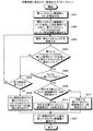
次に、キャッシュメモリ装置200が行うエラー処理について説明する。図10は、本実施例に係るエラー処理を示すフローチャートである。同図に示すように、第1レベルキャッシュ制御部220にエラーが発生し(ステップS201)、エラー検出部230cが、第2レベルキャッシュ制御部250にエラーが発生した旨を通知すると共に、第1レベルキャッシュインデックスA2およびエラーウェイ特定情報を通知する(ステップS202)。
Next, error processing performed by the
そして、エラー処理部260bは、順次、第2レベルキャッシュタグを検索し(ステップS203)、第1レベルキャッシュインデックスA2と等しい仮想インデックスを含んだ第2レベルキャッシュタグを検出したか否かを判断する(ステップS204)。
Then, the
第1レベルキャッシュインデックスA2と等しい仮想インデックスを含んだ第2レベルキャッシュタグを検出しなかった場合には(ステップS204,No)、全て検索が終了したか否かを判断し(ステップS205)、全て検索が終了していない場合には(ステップS205,No)、ステップS203に移行する。 When the second level cache tag including the virtual index equal to the first level cache index A2 is not detected (No at Step S204), it is determined whether or not the search is completed (Step S205). If the search is not completed (No at Step S205), the process proceeds to Step S203.
一方、全て検索が終了した場合には(ステップS205,Yes)、エラー処理部260bは、エラー報告を受付けた第1レベルインデックスA2とウェイに対応するデータの無効化指示を行い(ステップS206)、エラー処理が完了した旨を第1レベルキャッシュ制御部220に通知する(ステップS207)。
On the other hand, if all the searches are completed (step S205, Yes), the
ところで、第1レベルキャッシュインデックスA2と等しい仮想インデックスを含んだ第2レベルキャッシュタグを検出した場合には(ステップS204,Yes)、ウェイが一致するか否かを判定し(ステップS208)、ウェイが一致しない場合には(ステップS208,No)、ステップS205に移行する。 By the way, when a second level cache tag including a virtual index equal to the first level cache index A2 is detected (Yes in step S204), it is determined whether the ways match (step S208). If they do not match (step S208, No), the process proceeds to step S205.
一方、ウェイが一致する場合には(ステップS208,Yes)、対応する第1レベルキャッシュ制御部220のデータが更新型か否かを判定し(ステップS209)、更新型である場合には(ステップS209,Yes)、対応する第1レベルキャッシュ制御部220のデータを吐き出し(ステップS211)、ステップS207に移行する。
On the other hand, if the ways match (step S208, Yes), it is determined whether or not the data in the corresponding first level
一方、更新型でない場合には(ステップS209,No)、対応する第1レベルキャッシュ制御部220のデータを無効化し(ステップS210)、ステップS207に移行する。
On the other hand, if it is not the update type (No at Step S209), the corresponding data in the first level
上述してきたように、本実施例に係るキャッシュメモリ装置200は、第2レベルキャッシュタグに第1レベルキャッシュ制御部220の登録情報を記憶させる。そして、コヒーレンシ維持処理部260aは、第1レベルキャッシュ制御部220からメモリアクセス要求を受けた場合に、該当する第2レベルキャッシュタグを検索し、プロセッサの要求するデータを第1レベルキャッシュに転送すると共に、第2レベルキャッシュに記録された登録情報を基にして、第1レベルキャッシュ制御部220および第2レベルキャッシュ制御部間のコヒーレンシを維持するので、タグの2段階アクセスを回避し、キャッシュメモリ装置200のマシンサイクルを高速化することができる。
As described above, the
また、従来のように、第1キャッシュメモリタグの写しを、第2レベルキャッシュ制御部250の記憶部270に記録される必要がないため、物量を削減することが可能となる。
Further, unlike the prior art, it is not necessary to record a copy of the first cache memory tag in the
(付記1)データ部およびタグ部からなる第1レベルキャッシュメモリ部と、該第1レベルキャッシュメモリ部を包含する第2レベルキャッシュメモリ部とを有し、プロセッサの要求に応答して該当するデータを前記プロセッサに渡すキャッシュメモリ装置であって、
前記第1レベルキャッシュメモリ部に係る情報の一部を記憶する記憶手段と、
前記記憶手段に記憶された情報を基にして、前記第1レベルキャッシュメモリ部と、前記第2レベルキャッシュメモリ部との間で、キャッシュコヒーレンシを維持するコヒーレンシ維持手段と、
を備えたことを特徴とするキャッシュメモリ装置。
(Additional remark 1) It has the 1st level cache memory part which consists of a data part and a tag part, and the 2nd level cache memory part which contains this 1st level cache memory part, and responds to the request | requirement of a processor, and applicable data A cache memory device for passing to the processor,
Storage means for storing a part of information relating to the first level cache memory unit;
Coherency maintaining means for maintaining cache coherency between the first level cache memory unit and the second level cache memory unit based on the information stored in the storage unit;
A cache memory device comprising:
(付記2)前記記憶手段は、前記第2レベルキャッシュメモリ部に対するタグの物理アドレス、ステータス、仮想インデックスおよび前記第1レベルキャッシュメモリ部に係る情報の一部を関連付けて記憶することを特徴とする付記1に記載のキャッシュメモリ装置。 (Supplementary Note 2) The storage means stores a physical address of a tag for the second level cache memory unit, a status, a virtual index, and a part of information related to the first level cache memory unit in association with each other. The cache memory device according to appendix 1.
(付記3)前記第1レベルキャッシュメモリ部に係る情報の一部は、複数のビットによって構成され、前記コヒーレンシ維持手段は、前記複数のビットから前記第1レベルキャッシュメモリ部の登録状態を把握し、前記第1レベルキャッシュメモリ部と、前記第2レベルキャッシュメモリ部との間で、キャッシュコヒーレンシを維持することを特徴とする付記1または2に記載のキャッシュメモリ装置。 (Supplementary Note 3) A part of the information related to the first level cache memory unit is constituted by a plurality of bits, and the coherency maintaining means grasps the registration state of the first level cache memory unit from the plurality of bits. The cache memory device according to appendix 1 or 2, wherein cache coherency is maintained between the first level cache memory unit and the second level cache memory unit.
(付記4)前記第1レベルキャッシュメモリ部に対するタグの物理アドレス、ステータスおよび第2レベルキャッシュメモリ部に登録されたウェイの情報を関連付けて記憶する第1キャッシュ記憶手段を更に備えたことを特徴とする付記1に記載のキャッシュメモリ装置。 (Additional remark 4) It is characterized by further comprising first cache storage means for storing the physical address of the tag for the first level cache memory unit, the status, and the way information registered in the second level cache memory unit in association with each other. The cache memory device according to appendix 1.
(付記5)前記第1レベルキャッシュメモリ部にエラーが発生した場合に、前記記憶手段に記憶された情報と、前記第1キャッシュ記憶手段に記憶された情報とを基にして、前記第1レベルキャッシュメモリ部に発生したエラーを修正する修正手段をさらに備えたことを特徴とする付記4に記載のキャッシュメモリ装置。 (Supplementary Note 5) When an error occurs in the first level cache memory unit, the first level is determined based on the information stored in the storage unit and the information stored in the first cache storage unit. The cache memory device according to appendix 4, further comprising a correcting unit that corrects an error occurring in the cache memory unit.
(付記6)前記修正手段は、前記第1レベルキャッシュメモリ部にエラーが発生した場合に、エラーの発生したデータを示すエラーデータが更新されている可能性があるか否かを判定し、更新されている可能性がある場合には、前記エラーデータを第2レベルキャッシュメモリ部に吐き出し、更新されている可能性がない場合には、前記エラーデータを無効化することを特徴とする付記5に記載のキャッシュメモリ装置。 (Supplementary Note 6) When the error occurs in the first level cache memory unit, the correction unit determines whether there is a possibility that the error data indicating the data in which the error has occurred is updated, and updates If there is a possibility of being updated, the error data is discharged to the second level cache memory unit, and if there is no possibility of being updated, the error data is invalidated. The cache memory device according to 1.
(付記7)データ部およびタグ部からなる第1レベルキャッシュメモリ部と、該第1レベルキャッシュメモリ部を包含する第2レベルキャッシュメモリ部とを有し、プロセッサの要求に応答して該当するデータを前記プロセッサに渡すキャッシュメモリ装置を制御するキャッシュメモリ制御方法であって、
前記第1レベルキャッシュメモリ部に係る情報の一部を記憶装置に記憶する記憶工程と、
前記記憶装置に記憶された情報を基にして、前記第1レベルキャッシュメモリ部と、前記第2レベルキャッシュメモリ部との間で、キャッシュコヒーレンシを維持するコヒーレンシ維持工程と、
を含んだことを特徴とするキャッシュメモリ制御方法。
(Additional remark 7) It has the 1st level cache memory part which consists of a data part and a tag part, and the 2nd level cache memory part which contains this 1st level cache memory part, and responds to the request | requirement of a processor, and applicable data A cache memory control method for controlling a cache memory device that passes the data to the processor,
A storage step of storing a part of information related to the first level cache memory unit in a storage device;
A coherency maintaining step of maintaining cache coherency between the first level cache memory unit and the second level cache memory unit based on information stored in the storage device;
A cache memory control method comprising:
(付記8)前記記憶装置は、前記第2レベルキャッシュメモリ部に対するタグの物理アドレス、ステータス、仮想インデックスおよび前記第1レベルキャッシュメモリ部に係る情報の一部を関連付けて記憶することを特徴とする付記7に記載のキャッシュメモリ制御方法。 (Supplementary Note 8) The storage device stores a physical address of a tag for the second level cache memory unit, a status, a virtual index, and a part of information related to the first level cache memory unit in association with each other. The cache memory control method according to appendix 7.
(付記9)データ部およびタグ部からなる第1レベルキャッシュメモリ部と、該第1レベルキャッシュメモリ部を包含する第2レベルキャッシュメモリ部とを有し、プロセッサの要求に応答して該当するデータを前記プロセッサに渡すキャッシュメモリ装置を制御するキャッシュメモリ制御方法であって、
前記第1レベルキャッシュメモリ部に係る情報の一部を記憶装置に記憶する記憶工程と、
前記第1レベルのキャッシュメモリ部にエラーが発生した場合に、前記記憶装置に記憶された情報を基にして、前記第1キャッシュメモリ部に発生したエラーを修正する修正工程と、
を含んだことを特徴とするキャッシュメモリ制御方法。
(Additional remark 9) It has the 1st level cache memory part which consists of a data part and a tag part, and the 2nd level cache memory part which contains this 1st level cache memory part, and responds to the request | requirement of a processor, and applicable data A cache memory control method for controlling a cache memory device that passes the data to the processor,
A storage step of storing a part of information related to the first level cache memory unit in a storage device;
A correction step of correcting an error generated in the first cache memory unit based on information stored in the storage device when an error occurs in the first level cache memory unit;
A cache memory control method comprising:
(付記10)前記修正工程は、前記第1レベルキャッシュメモリ部にエラーが発生した場合に、エラーの発生したデータを示すエラーデータが更新されている可能性があるか否かを判定し、更新されている可能性がある場合には、前記エラーデータを第2レベルキャッシュメモリ部に吐き出し、更新されている可能性がない場合には、前記エラーデータを無効化することを特徴とする付記9に記載のキャッシュメモリ制御方法。 (Supplementary Note 10) When the error occurs in the first level cache memory unit, the correction step determines whether there is a possibility that the error data indicating the data in which the error has occurred is updated, and updates If there is a possibility of being updated, the error data is discharged to the second level cache memory unit, and if there is no possibility of being updated, the error data is invalidated. 2. A cache memory control method according to 1.
以上のように、本発明にかかるキャッシュメモリ装置およびキャッシュメモリ制御方法は、キャッシュメモリなどに対して有用であり、特に、マシンサイクルを高速化させる場合に適している。 As described above, the cache memory device and the cache memory control method according to the present invention are useful for a cache memory and the like, and are particularly suitable for increasing the machine cycle speed.
100 プロセッサ
200 キャッシュメモリ装置
210 命令実行制御部
220 第1レベルキャッシュ制御部
230 第1レベルキャッシュブロック部
230a アドレス変換処理部
230b 検索処理部
230c エラー検出部
240,270 記憶部
240a 命令キャッシュタグ部
240b 命令キャッシュデータ部
240c オペランドキャッシュタグ部
240d オペランドキャッシュデータ部
250 第2レベルキャッシュ制御部
260 第2レベルキャッシュブロック部
260a コヒーレンシ維持処理部
260b エラー処理部
270a 第2レベルキャッシュタグ部
270b 第2レベルキャッシュデータ部
300 メインメモリ
100
Claims (13)
前記1次キャッシュメモリは、 The primary cache memory is
データを登録する1次キャッシュデータ部と、 A primary cache data section for registering data;
前記1次キャッシュデータ部が登録するデータについてのタグであって、第1の物理アドレスを含む1次キャッシュタグを保持する1次キャッシュタグ部と、 A tag for data registered by the primary cache data part, a primary cache tag part for holding a primary cache tag including a first physical address;
前記演算処理部が出力したメモリアクセス要求に含まれ、1次キャッシュインデックスを含む仮想アドレスを、タグ比較アドレスと2次キャッシュインデックスとを含む物理アドレスに変換するアドレス変換処理部と、 An address conversion processing unit that converts a virtual address that is included in the memory access request output by the arithmetic processing unit and includes a primary cache index into a physical address that includes a tag comparison address and a secondary cache index;
1次キャッシュインデックスを用いて前記1次キャッシュタグ部を検索し、前記検索された1次キャッシュタグが含む第1の物理アドレスとタグ比較アドレスを比較し、一致の場合には、前記第1の物理アドレスに対応する前記1次キャッシュデータ部が登録するデータを前記演算処理部に出力し、不一致の場合には、前記1次キャッシュインデックスと前記物理アドレスを出力する第1の検索処理部を有し、 The primary cache tag portion is searched using a primary cache index, and a first physical address included in the searched primary cache tag is compared with a tag comparison address. Data registered in the primary cache data part corresponding to the physical address is output to the arithmetic processing part, and if there is a mismatch, a first search processing part for outputting the primary cache index and the physical address is provided. And
前記2次キャッシュメモリは、 The secondary cache memory is
前記1次キャッシュデータ部が登録するデータを記憶する2次キャッシュデータ部と、 A secondary cache data portion for storing data registered by the primary cache data portion;
前記2次キャッシュデータ部が保持するデータについてのタグであって、第2の物理アドレスと、仮想インデックスと、前記2次キャッシュデータ部が保持する前記1次キャッシュデータ部に登録されたデータについての登録情報である1次キャッシュ登録情報とを含む2次キャッシュタグを保持する2次キャッシュタグ部と、 A tag for data held by the secondary cache data part, the second physical address, a virtual index, and data registered in the primary cache data part held by the secondary cache data part A secondary cache tag portion that holds a secondary cache tag including primary cache registration information that is registration information;
前記第1の検索処理部が出力した物理アドレスに含まれる2次キャッシュインデックスを用いて前記2次キャッシュタグ部を検索し、前記検索された2次キャッシュタグが含む第2の物理アドレスと前記第1の検索処理部が出力した物理アドレスに含まれるタグ比較アドレスを比較し、一致の場合には、前記第1の検索処理部が出力した前記1次キャッシュインデックスと検索された2次キャッシュタグが含む仮想インデックスをさらに比較し、前記1次キャッシュインデックスと前記仮想インデックスが一致する場合には、前記第2の物理アドレスに対応する前記2次キャッシュデータ部が保持するデータを前記1次キャッシュデータ部に登録するとともに前記演算処理部に出力し、前記1次キャッシュインデックスと前記仮想インデックスが一致しない場合には、前記検索された2次キャッシュタグが含む1次キャッシュ登録情報に基づき、前記仮想インデックスに対応するデータが前記1次キャッシュデータ部に登録され且つ前記2次キャッシュデータ部が保持する前記1次キャッシュデータ部に登録されたデータを前記演算処理部が書き換え得る更新型であると判断した場合には、前記仮想インデックスに対応する前記1次キャッシュデータデータ部から出力させたデータを前記2次キャッシュデータ部に保持させるコヒーレンシ維持部を有することを特徴とするキャッシュメモリ装置。 The secondary cache tag part is searched using a secondary cache index included in the physical address output by the first search processing part, and the second physical address included in the searched secondary cache tag and the first A tag comparison address included in the physical address output by the first search processing unit is compared. If they match, the primary cache index output by the first search processing unit and the searched secondary cache tag are When the virtual cache is further compared, and the primary cache index matches the virtual index, the data held in the secondary cache data portion corresponding to the second physical address is stored in the primary cache data portion. And the first cache index and the virtual index are output to the arithmetic processing unit. Are not matched, the data corresponding to the virtual index is registered in the primary cache data portion based on the primary cache registration information included in the searched secondary cache tag, and the secondary cache data portion is If it is determined that the data registered in the held primary cache data part is an update type that can be rewritten by the arithmetic processing part, the data output from the primary cache data data part corresponding to the virtual index A cache memory device comprising a coherency maintaining unit that holds the data in the secondary cache data unit.
前記コヒーレンシ維持部はさらに、 The coherency maintenance unit further includes:
前記1次キャッシュインデックスと前記仮想インデックスが一致しない場合であって、前記検索された2次キャッシュタグが含む1次キャッシュ登録情報に基づき、前記仮想インデックスに対応するデータが前記1次キャッシュデータ部に登録され且つ前記更新型でないと判断した場合には、前記仮想インデックスに対応する前記1次キャッシュデータ部が登録するデータを無効化することを特徴とする請求項1記載のキャッシュメモリ装置。 When the primary cache index and the virtual index do not match, data corresponding to the virtual index is stored in the primary cache data section based on primary cache registration information included in the searched secondary cache tag. 2. The cache memory device according to claim 1, wherein when it is determined that the data is registered and is not the update type, data registered by the primary cache data unit corresponding to the virtual index is invalidated.
前記コヒーレンシ維持部はさらに、 The coherency maintenance unit further includes:
前記1次キャッシュインデックスと前記仮想インデックスが一致しない場合であって、前記検索された2次キャッシュタグが含む1次キャッシュ登録情報に基づき、前記仮想インデックスに対応するデータが前記1次キャッシュデータ部に登録されていないと判断した場合には、前記第2の物理アドレスに対応する前記2次キャッシュデータ部が保持するデータを前記1次キャッシュデータ部に登録することを特徴とする請求項2記載のキャッシュメモリ装置。 When the primary cache index and the virtual index do not match, data corresponding to the virtual index is stored in the primary cache data section based on primary cache registration information included in the searched secondary cache tag. 3. The data stored in the secondary cache data part corresponding to the second physical address is registered in the primary cache data part when it is determined that it is not registered. Cache memory device.
前記2次キャッシュメモリ部は複数のウェイを有し、 The secondary cache memory unit has a plurality of ways,
前記1次キャッシュタグはさらに、前記1次キャッシュメモリ部が登録するデータが前記2次キャッシュメモリ部のどのウェイに登録されているかを示すウェイ特定情報を含み、 The primary cache tag further includes way specifying information indicating in which way of the secondary cache memory unit data registered by the primary cache memory unit is registered,
前記1次キャッシュメモリはさらに、 The primary cache memory further includes
検出した前記1次キャッシュデータ部又は前記1次キャッシュタグ部にエラーが発生した旨と、前記エラーが発生したデータに対応する1次キャッシュタグに含まれる1次キャッシュインデックスと前記エラーが発生したウェイを特定するエラーウェイ特定情報を前記2次キャッシュメモリに通知するエラー検出部を有し、 The fact that an error has occurred in the detected primary cache data part or the primary cache tag part, the primary cache index included in the primary cache tag corresponding to the data in which the error has occurred, and the way in which the error has occurred An error detection unit for notifying the secondary cache memory of error way specifying information for specifying
前記2次キャッシュメモリはさらに、 The secondary cache memory further includes
前記エラー検出部が通知した1次キャッシュインデックスを用いて前記2次キャッシュタグ部を検索し、前記1次キャッシュインデックスと等しい仮想インデックスを含む2次キャッシュタグが検索された場合、前記検索された2次キャッシュタグが含む1次キャッシュ登録情報が含むウェイ特定情報と前記エラー検出部が通知したエラーウェイ特定情報を比較し、一致の場合には、前記検索された2次キャッシュタグが含む1次キャッシュ登録情報に基づき、前記仮想インデックスに対応するデータが前記1次キャッシュデータ部に登録され且つ更新型であると判断した場合には、前記1次キャッシュデータ部から出力させた前記仮想インデックスに対応するデータを前記2次キャッシュデータ部に保持させるエラー処理部を有することを特徴とする請求項1記載のキャッシュメモリ装置。 When the secondary cache tag part is searched using the primary cache index notified by the error detection part and a secondary cache tag including a virtual index equal to the primary cache index is searched, the searched 2 The way identification information included in the primary cache registration information included in the next cache tag is compared with the error way identification information notified by the error detection unit. If they match, the primary cache included in the searched secondary cache tag is compared. Based on the registration information, if it is determined that the data corresponding to the virtual index is registered in the primary cache data part and is of the update type, it corresponds to the virtual index output from the primary cache data part Having an error processing unit for holding data in the secondary cache data unit; Cache memory apparatus according to claim 1, symptoms.
前記エラー処理部は、 The error processing unit
前記検索された2次キャッシュタグが含む1次キャッシュ登録情報に基づき、前記仮想インデックスに対応するデータが前記1次キャッシュデータ部に登録され且つ前記更新型でないと判断した場合には、前記仮想インデックスに対応する前記1次キャッシュデータ部が登録するデータを無効化することを特徴とする請求項4記載のキャッシュメモリ装置。 When it is determined that the data corresponding to the virtual index is registered in the primary cache data part and is not the update type based on the primary cache registration information included in the searched secondary cache tag, the virtual index 5. The cache memory device according to claim 4, wherein the data registered by the primary cache data section corresponding to is invalidated.
前記エラー処理部は、 The error processing unit
前記検索された2次キャッシュタグが含む1次キャッシュ登録情報が含むウェイ特定情報と前記エラー検出部が通知したエラーウェイ特定情報を比較し、全てのタグが不一致の場合には、前記1次キャッシュインデックスに対応する前記1次キャッシュデータ部が登録するデータと前記エラー検出部が通知したエラーウェイ特定情報に対応する前記2次キャッシュデータ部のウェイに保持されるデータを無効化することを特徴とする請求項4記載のキャッシュメモリ装置。 The way identification information included in the primary cache registration information included in the retrieved secondary cache tag is compared with the error way identification information notified by the error detection unit. If all the tags do not match, the primary cache is included. The data registered in the primary cache data part corresponding to the index and the data held in the way of the secondary cache data part corresponding to the error way specifying information notified by the error detection part are invalidated. The cache memory device according to claim 4.
前記1次キャッシュメモリは、 The primary cache memory is
データを登録する1次キャッシュデータ部と、 A primary cache data section for registering data;
前記1次キャッシュデータ部が登録するデータについてのタグであって、第1の物理アドレスを含む1次キャッシュタグを保持する1次キャッシュタグ部と、 A tag for data registered by the primary cache data part, a primary cache tag part for holding a primary cache tag including a first physical address;
前記演算処理部が出力したメモリアクセス要求に含まれ、1次キャッシュインデックスを含む仮想アドレスを、タグ比較アドレスと2次キャッシュインデックスとを含む物理アドレスに変換するアドレス変換処理部と、 An address conversion processing unit that converts a virtual address that is included in the memory access request output by the arithmetic processing unit and includes a primary cache index into a physical address that includes a tag comparison address and a secondary cache index;
1次キャッシュインデックスを用いて前記1次キャッシュタグ部を検索し、前記検索された1次キャッシュタグが含む第1の物理アドレスとタグ比較アドレスを比較し、一致の場合には、前記第1の物理アドレスに対応する前記1次キャッシュデータ部が登録するデータを前記演算処理部に出力し、不一致の場合には、前記1次キャッシュインデックスと前記物理アドレスを出力する第1の検索処理部を有し、 The primary cache tag portion is searched using a primary cache index, and a first physical address included in the searched primary cache tag is compared with a tag comparison address. Data registered in the primary cache data part corresponding to the physical address is output to the arithmetic processing part, and if there is a mismatch, a first search processing part for outputting the primary cache index and the physical address is provided. And
前記2次キャッシュメモリは、 The secondary cache memory is
前記1次キャッシュデータ部が登録するデータを記憶する2次キャッシュデータ部と、 A secondary cache data portion for storing data registered by the primary cache data portion;
前記2次キャッシュデータ部が保持するデータについてのタグであって、第2の物理アドレスと、仮想インデックスと、前記2次キャッシュデータ部が保持する前記1次キャッシュデータ部に登録されたデータについての登録情報である1次キャッシュ登録情報とを含む2次キャッシュタグを保持する2次キャッシュタグ部と、 A tag for data held by the secondary cache data part, the second physical address, a virtual index, and data registered in the primary cache data part held by the secondary cache data part A secondary cache tag portion that holds a secondary cache tag including primary cache registration information that is registration information;
前記第1の検索処理部が出力した物理アドレスに含まれる2次キャッシュインデックスを用いて前記2次キャッシュタグ部を検索し、前記検索された2次キャッシュタグが含む第2の物理アドレスと前記第1の検索処理部が出力した物理アドレスに含まれるタグ比較アドレスを比較し、一致の場合には、前記第1の検索処理部が出力した前記1次キャッシュインデックスと検索された2次キャッシュタグが含む仮想インデックスをさらに比較し、前記1次キャッシュインデックスと前記仮想インデックスが一致する場合には、前記第2の物理アドレスに対応する前記2次キャッシュデータ部が保持するデータを前記1次キャッシュデータ部に登録するとともに前記演算処理部に出力し、前記1次キャッシュインデックスと前記仮想インデックスが一致しない場合には、前記検索された2次キャッシュタグが含む1次キャッシュ登録情報に基づき、前記仮想インデックスに対応するデータが前記1次キャッシュデータ部に登録され且つ前記2次キャッシュデータ部が保持する前記1次キャッシュデータ部に登録されたデータを前記演算処理部が書き換え得る更新型であると判断した場合には、前記仮想インデックスに対応する前記1次キャッシュデータデータ部から出力させたデータを前記2次キャッシュデータ部に保持させるコヒーレンシ維持部を有することを特徴とする演算処理装置。 The secondary cache tag part is searched using a secondary cache index included in the physical address output by the first search processing part, and the second physical address included in the searched secondary cache tag and the first A tag comparison address included in the physical address output by the first search processing unit is compared. If they match, the primary cache index output by the first search processing unit and the searched secondary cache tag are When the virtual cache is further compared, and the primary cache index matches the virtual index, the data held in the secondary cache data portion corresponding to the second physical address is stored in the primary cache data portion. And the first cache index and the virtual index are output to the arithmetic processing unit. Are not matched, the data corresponding to the virtual index is registered in the primary cache data portion based on the primary cache registration information included in the searched secondary cache tag, and the secondary cache data portion is When it is determined that the data registered in the held primary cache data part is an update type that can be rewritten by the arithmetic processing unit, the data output from the primary cache data data part corresponding to the virtual index And a coherency maintaining unit that holds the data in the secondary cache data unit.
前記コヒーレンシ維持部はさらに、 The coherency maintenance unit further includes:
前記1次キャッシュインデックスと前記仮想インデックスが一致しない場合であって、前記検索された2次キャッシュタグが含む1次キャッシュ登録情報に基づき、前記仮想インデックスに対応するデータが前記1次キャッシュデータ部に登録され且つ前記更新型でないと判断した場合には、前記仮想インデックスに対応する前記1次キャッシュデータ部が登録するデータを無効化することを特徴とする請求項7記載の演算処理装置。 When the primary cache index and the virtual index do not match, data corresponding to the virtual index is stored in the primary cache data section based on primary cache registration information included in the searched secondary cache tag. 8. The arithmetic processing apparatus according to claim 7, wherein when it is determined that the registered data is not the update type, data registered by the primary cache data unit corresponding to the virtual index is invalidated.
前記コヒーレンシ維持部はさらに、 The coherency maintenance unit further includes:
前記1次キャッシュインデックスと前記仮想インデックスが一致しない場合であって、前記検索された2次キャッシュタグが含む1次キャッシュ登録情報に基づき、前記仮想インデックスに対応するデータが前記1次キャッシュデータ部に登録されていないと判断した場合には、前記第2の物理アドレスに対応する前記2次キャッシュデータ部が保持するデータを前記1次キャッシュデータ部に登録することを特徴とする請求項7記載の演算処理装置。 When the primary cache index and the virtual index do not match, data corresponding to the virtual index is stored in the primary cache data section based on primary cache registration information included in the searched secondary cache tag. 8. The data stored in the secondary cache data part corresponding to the second physical address is registered in the primary cache data part when it is determined that the data is not registered. Arithmetic processing unit.
前記2次キャッシュメモリ部は複数のウェイを有し、 The secondary cache memory unit has a plurality of ways,
前記1次キャッシュタグはさらに、前記1次キャッシュメモリ部が登録するデータが前記2次キャッシュメモリ部のどのウェイに登録されているかを示すウェイ特定情報を含み、 The primary cache tag further includes way specifying information indicating in which way of the secondary cache memory unit data registered by the primary cache memory unit is registered,
前記1次キャッシュメモリはさらに、 The primary cache memory further includes
検出した前記1次キャッシュデータ部又は前記1次キャッシュタグ部にエラーが発生した旨と、前記エラーが発生したデータに対応する1次キャッシュタグに含まれる1次キャッシュインデックスと前記エラーが発生したウェイを特定するエラーウェイ特定情報を前記2次キャッシュメモリに通知するエラー検出部を有し、 The fact that an error has occurred in the detected primary cache data part or the primary cache tag part, the primary cache index included in the primary cache tag corresponding to the data in which the error has occurred, and the way in which the error has occurred An error detection unit for notifying the secondary cache memory of error way specifying information for specifying
前記2次キャッシュメモリはさらに、 The secondary cache memory further includes
前記エラー検出部が通知した1次キャッシュインデックスを用いて前記2次キャッシュタグ部を検索し、前記1次キャッシュインデックスと等しい仮想インデックスを含む2次キャッシュタグが検索された場合、前記検索された2次キャッシュタグが含む1次キャッシュ登録情報が含むウェイ特定情報と前記エラー検出部が通知したエラーウェイ特定情報を比較し、一致の場合には、前記検索された2次キャッシュタグが含む1次キャッシュ登録情報に基づき、前記仮想インデックスに対応するデータが前記1次キャッシュデータ部に登録され且つ更新型であると判断した場合には、前記1次キャッシュデータ部から出力させた前記仮想インデックスに対応するデータを前記2次キャッシュデータ部に保持させるエラー処理部を有することを特徴とする請求項7記載の演算処理装置。 When the secondary cache tag part is searched using the primary cache index notified by the error detection part and a secondary cache tag including a virtual index equal to the primary cache index is searched, the searched 2 The way identification information included in the primary cache registration information included in the next cache tag is compared with the error way identification information notified by the error detection unit. If they match, the primary cache included in the searched secondary cache tag is compared. Based on the registration information, if it is determined that the data corresponding to the virtual index is registered in the primary cache data part and is of the update type, it corresponds to the virtual index output from the primary cache data part Having an error processing unit for holding data in the secondary cache data unit; Processing unit according to claim 7, symptoms.
前記エラー処理部は、 The error processing unit
前記検索された2次キャッシュタグが含む1次キャッシュ登録情報に基づき、前記仮想インデックスに対応するデータが前記1次キャッシュデータ部に登録され且つ前記更新型でないと判断した場合には、前記仮想インデックスに対応する前記1次キャッシュデータ部が登録するデータを無効化することを特徴とする請求項10記載の演算処理装置。 When it is determined that the data corresponding to the virtual index is registered in the primary cache data part and is not the update type based on the primary cache registration information included in the retrieved secondary cache tag, the virtual index 11. The arithmetic processing apparatus according to claim 10, wherein the data registered by the primary cache data section corresponding to is invalidated.
前記エラー処理部は、 The error processing unit
前記検索された2次キャッシュタグが含む1次キャッシュ登録情報が含むウェイ特定情報と前記エラー検出部が通知したエラーウェイ特定情報を比較し、全てのタグが不一致の場合には、前記1次キャッシュインデックスに対応する前記1次キャッシュデータ部が登録するデータと前記エラー検出部が通知したエラーウェイ特定情報に対応する前記2次キャッシュデータ部のウェイに保持されるデータを無効化することを特徴とする請求項10記載の演算処理装置。 The way identification information included in the primary cache registration information included in the retrieved secondary cache tag is compared with the error way identification information notified by the error detection unit. If all the tags do not match, the primary cache is included. The data registered in the primary cache data part corresponding to the index and the data held in the way of the secondary cache data part corresponding to the error way specifying information notified by the error detection part are invalidated. The arithmetic processing device according to claim 10.
前記1次キャッシュメモリが有するアドレス変換処理部が、前記演算処理部が出力したメモリアクセス要求に含まれ、1次キャッシュインデックスを含む仮想アドレスを、タグ比較アドレスと2次キャッシュインデックスとを含む物理アドレスに変換するステップと、 The address conversion processing unit included in the primary cache memory is included in the memory access request output from the arithmetic processing unit, and a virtual address including the primary cache index is represented as a physical address including a tag comparison address and a secondary cache index. Converting to
前記1次キャッシュメモリが有する第1の検索処理部が、1次キャッシュインデックスを用いて前記1次キャッシュタグ部を検索し、前記検索された1次キャッシュタグが含む第1の物理アドレスとタグ比較アドレスを比較し、一致の場合には、前記第1の物理アドレスに対応する前記1次キャッシュデータ部が登録するデータを前記演算処理部に出力し、不一致の場合には、前記1次キャッシュインデックスと前記物理アドレスを出力するステップと、 A first search processing unit included in the primary cache memory searches the primary cache tag unit using a primary cache index, and compares the tag with a first physical address included in the searched primary cache tag. The addresses are compared, and if they match, the data registered by the primary cache data part corresponding to the first physical address is output to the arithmetic processing part, and if they do not match, the primary cache index And outputting the physical address;
前記2次キャッシュメモリが有するコヒーレンシ維持部が、前記第1の検索処理部が出力した物理アドレスに含まれる2次キャッシュインデックスを用いて前記2次キャッシュタグ部を検索するステップと、 A step in which a coherency maintaining unit included in the secondary cache memory searches the secondary cache tag unit using a secondary cache index included in the physical address output by the first search processing unit;
前記コヒーレンシ維持部が、前記検索された2次キャッシュタグが含む第2の物理アドレスと前記第1の検索処理部が出力した物理アドレスに含まれるタグ比較アドレスを比較するステップと、 The coherency maintaining unit comparing a second physical address included in the searched secondary cache tag with a tag comparison address included in the physical address output by the first search processing unit;
前記比較の結果、一致の場合には、前記コヒーレンシ維持部が、前記第1の検索処理部が出力した前記1次キャッシュインデックスと検索された2次キャッシュタグが含む仮想インデックスを更に比較し、前記1次キャッシュインデックスと前記仮想インデックスが一致する場合には、前記第2の物理アドレスに対応する前記2次キャッシュデータ部が保持するデータを前記1次キャッシュデータ部に登録するとともに前記演算処理部に出力し、前記1次キャッシュインデックスと前記仮想インデックスが一致しない場合には、前記検索された2次キャッシュタグが含む1次キャッシュ登録情報に基づき、前記仮想インデックスに対応するデータが前記1次キャッシュデータ部に登録され且つ前記2次キャッシュデータ部が保持する前記1次キャッシュデータ部に登録されたデータを前記演算処理部が書き換え得る更新型であると判断した場合には、前記仮想インデックスに対応する前記1次キャッシュデータ部から出力させたデータを前記2次キャッシュデータ部に保持させるステップを有することを特徴とするキャッシュメモリ装置の制御方法。 If the result of the comparison is a match, the coherency maintaining unit further compares the primary cache index output from the first search processing unit with the virtual index included in the searched secondary cache tag, If the primary cache index and the virtual index match, the data held in the secondary cache data part corresponding to the second physical address is registered in the primary cache data part and is stored in the arithmetic processing part. When the primary cache index and the virtual index do not match, the data corresponding to the virtual index is the primary cache data based on the primary cache registration information included in the searched secondary cache tag. The primary data stored in the secondary cache data part and stored in the secondary cache data part When it is determined that the data registered in the cache data unit is an update type that can be rewritten by the arithmetic processing unit, the data output from the primary cache data unit corresponding to the virtual index is the secondary cache data unit. A method for controlling a cache memory device, comprising the step of:
Priority Applications (3)
| Application Number | Priority Date | Filing Date | Title |
|---|---|---|---|
| JP2004222401A JP4673584B2 (en) | 2004-07-29 | 2004-07-29 | Cache memory device, arithmetic processing device, and control method for cache memory device |
| US10/998,561 US7428617B2 (en) | 2004-07-29 | 2004-11-30 | Cache memory and method to maintain cache-coherence between cache memory units |
| EP04257443A EP1622028B1 (en) | 2004-07-29 | 2004-11-30 | Cache memory and method for controlling cache memory |
Applications Claiming Priority (1)
| Application Number | Priority Date | Filing Date | Title |
|---|---|---|---|
| JP2004222401A JP4673584B2 (en) | 2004-07-29 | 2004-07-29 | Cache memory device, arithmetic processing device, and control method for cache memory device |
Publications (2)
| Publication Number | Publication Date |
|---|---|
| JP2006040175A JP2006040175A (en) | 2006-02-09 |
| JP4673584B2 true JP4673584B2 (en) | 2011-04-20 |
Family
ID=35170058
Family Applications (1)
| Application Number | Title | Priority Date | Filing Date |
|---|---|---|---|
| JP2004222401A Expired - Fee Related JP4673584B2 (en) | 2004-07-29 | 2004-07-29 | Cache memory device, arithmetic processing device, and control method for cache memory device |
Country Status (3)
| Country | Link |
|---|---|
| US (1) | US7428617B2 (en) |
| EP (1) | EP1622028B1 (en) |
| JP (1) | JP4673584B2 (en) |
Families Citing this family (23)
| Publication number | Priority date | Publication date | Assignee | Title |
|---|---|---|---|---|
| WO2007094048A1 (en) * | 2006-02-14 | 2007-08-23 | Fujitsu Limited | Invalidation processing device and invalidation processing method |
| WO2007094046A1 (en) * | 2006-02-14 | 2007-08-23 | Fujitsu Limited | Coherency maintaining device and coherency maintaining method |
| JPWO2007096998A1 (en) * | 2006-02-24 | 2009-07-09 | 富士通株式会社 | Cache memory device and cache memory control method |
| JP2008046685A (en) * | 2006-08-10 | 2008-02-28 | Fujitsu Ltd | Duplex system and system switching method |
| US8683139B2 (en) | 2006-10-31 | 2014-03-25 | Hewlett-Packard Development Company, L.P. | Cache and method for cache bypass functionality |
| US20080104333A1 (en) * | 2006-10-31 | 2008-05-01 | Veazey Judson E | Tracking of higher-level cache contents in a lower-level cache |
| US7657710B2 (en) * | 2006-11-17 | 2010-02-02 | Sun Microsystems, Inc. | Cache coherence protocol with write-only permission |
| JP5347306B2 (en) * | 2007-03-29 | 2013-11-20 | 宇部興産株式会社 | Seamless belt |
| US8019945B2 (en) * | 2008-01-31 | 2011-09-13 | Oracle International Corporation | System and method for transactional cache |
| JP5440067B2 (en) * | 2009-09-18 | 2014-03-12 | 富士通株式会社 | Cache memory control device and cache memory control method |
| WO2012015766A2 (en) | 2010-07-28 | 2012-02-02 | Rambus Inc. | Cache memory that supports tagless addressing |
| WO2013084315A1 (en) | 2011-12-07 | 2013-06-13 | 富士通株式会社 | Processing unit and method for controlling processing unit |
| EP3060993B1 (en) * | 2013-10-21 | 2023-03-08 | FLC Global, Ltd. | Final level cache system and corresponding method |
| US11822474B2 (en) | 2013-10-21 | 2023-11-21 | Flc Global, Ltd | Storage system and method for accessing same |
| US9559722B1 (en) | 2013-10-21 | 2017-01-31 | Marvell International Ltd. | Network devices and methods of generating low-density parity-check codes and performing corresponding encoding of data |
| US9454991B2 (en) | 2013-10-21 | 2016-09-27 | Marvell World Trade Ltd. | Caching systems and methods for hard disk drives and hybrid drives |
| US10097204B1 (en) | 2014-04-21 | 2018-10-09 | Marvell International Ltd. | Low-density parity-check codes for WiFi networks |
| KR102147993B1 (en) | 2013-11-14 | 2020-08-25 | 삼성전자주식회사 | Nonvolatile memory system and operating method thereof |
| JP6337570B2 (en) * | 2014-03-28 | 2018-06-06 | 富士通株式会社 | Arithmetic processing device and control method of arithmetic processing device |
| EP3138099A1 (en) | 2014-05-02 | 2017-03-08 | Marvell World Trade Ltd. | Caching systems and methods for hard disk drives and hybrid drives |
| CN106933750B (en) * | 2015-12-31 | 2020-08-21 | 北京国睿中数科技股份有限公司 | Verification method and device for data and state in multi-level cache |
| CN112997161A (en) * | 2018-06-18 | 2021-06-18 | Flc技术集团股份有限公司 | Method and apparatus for using storage system as main memory |
| US10769071B2 (en) * | 2018-10-10 | 2020-09-08 | Micron Technology, Inc. | Coherent memory access |
Citations (3)
| Publication number | Priority date | Publication date | Assignee | Title |
|---|---|---|---|---|
| US5003459A (en) * | 1988-04-01 | 1991-03-26 | Digital Equipment Corporation | Cache memory system |
| US5668968A (en) * | 1992-03-02 | 1997-09-16 | International Business Machines Corporation | Two-level virtual/real set associative cache system and method with improved synonym detection |
| US20020199151A1 (en) * | 2001-06-26 | 2002-12-26 | Zuraski Gerald D. | Using type bits to track storage of ECC and predecode bits in a level two cache |
Family Cites Families (8)
| Publication number | Priority date | Publication date | Assignee | Title |
|---|---|---|---|---|
| JPH0380030A (en) * | 1989-08-22 | 1991-04-04 | Kazunari Mikami | Pipeline device for milking |
| JP2822518B2 (en) * | 1989-12-20 | 1998-11-11 | 住友電気工業株式会社 | Method for forming metallized layer on aluminum nitride sintered body |
| JPH03193684A (en) * | 1989-12-20 | 1991-08-23 | Kobe Steel Ltd | Production of carbon or carbon composite material |
| EP0461926B1 (en) * | 1990-06-15 | 1998-09-02 | Compaq Computer Corporation | Multilevel inclusion in multilevel cache hierarchies |
| JP3132749B2 (en) | 1994-12-05 | 2001-02-05 | インターナショナル・ビジネス・マシーンズ・コーポレ−ション | Multiprocessor data processing system |
| US6115794A (en) | 1997-04-14 | 2000-09-05 | International Business Machines Corporation | Method and system of providing a pseudo-precise inclusivity scheme in a sectored cache memory for maintaining cache coherency within a data-processing system |
| US5867511A (en) * | 1997-04-14 | 1999-02-02 | International Business Machines Corporation | Method for high-speed recoverable directory access |
| JP2002055881A (en) | 2000-08-08 | 2002-02-20 | Hitachi Ltd | Realizing method of cache coincident control and data processor using the same |
-
2004
- 2004-07-29 JP JP2004222401A patent/JP4673584B2/en not_active Expired - Fee Related
- 2004-11-30 EP EP04257443A patent/EP1622028B1/en not_active Expired - Fee Related
- 2004-11-30 US US10/998,561 patent/US7428617B2/en active Active
Patent Citations (4)
| Publication number | Priority date | Publication date | Assignee | Title |
|---|---|---|---|---|
| US5003459A (en) * | 1988-04-01 | 1991-03-26 | Digital Equipment Corporation | Cache memory system |
| US5668968A (en) * | 1992-03-02 | 1997-09-16 | International Business Machines Corporation | Two-level virtual/real set associative cache system and method with improved synonym detection |
| US20020199151A1 (en) * | 2001-06-26 | 2002-12-26 | Zuraski Gerald D. | Using type bits to track storage of ECC and predecode bits in a level two cache |
| JP2004531837A (en) * | 2001-06-26 | 2004-10-14 | アドバンスト・マイクロ・ディバイシズ・インコーポレイテッド | Use of Type Bits to Track ECC and Predecode Bit Storage in Level 2 Cache |
Also Published As
| Publication number | Publication date |
|---|---|
| EP1622028A2 (en) | 2006-02-01 |
| EP1622028B1 (en) | 2012-02-15 |
| EP1622028A3 (en) | 2008-05-21 |
| JP2006040175A (en) | 2006-02-09 |
| US7428617B2 (en) | 2008-09-23 |
| US20060026355A1 (en) | 2006-02-02 |
Similar Documents
| Publication | Publication Date | Title |
|---|---|---|
| JP4673584B2 (en) | Cache memory device, arithmetic processing device, and control method for cache memory device | |
| TWI381275B (en) | Address translation method and apparatus | |
| JP4297968B2 (en) | Coherency maintenance device and coherency maintenance method | |
| JP5526626B2 (en) | Arithmetic processing device and address conversion method | |
| JP3587591B2 (en) | Method of controlling cache miss and computer system thereof | |
| TWI519955B (en) | Prefetcher, method of prefetch data and computer program product | |
| JP3936378B2 (en) | Address translation device | |
| US20130173882A1 (en) | Instruction fetch translation lookaside buffer management to support host and guest o/s translations | |
| US8190973B2 (en) | Apparatus and method for error correction of data values in a storage device | |
| JP2018504694A (en) | Cache accessed using virtual address | |
| US8601240B2 (en) | Selectively defering load instructions after encountering a store instruction with an unknown destination address during speculative execution | |
| JPH0619793A (en) | History table of virtual address conversion estimation for cache access | |
| US9720847B2 (en) | Least recently used (LRU) cache replacement implementation using a FIFO storing indications of whether a way of the cache was most recently accessed | |
| JP2009512943A (en) | Multi-level translation index buffer (TLBs) field updates | |
| KR20220100939A (en) | Techniques for performing store-to-load forwarding | |
| TW201810046A (en) | Method and device for accessing a cache memory | |
| US20090019306A1 (en) | Protecting tag information in a multi-level cache hierarchy | |
| JP2007048296A (en) | Method, apparatus and system for invalidating multiple address cache entries | |
| US20070186046A1 (en) | Pseudo LRU algorithm for hint-locking during software and hardware address translation cache miss handling modes | |
| WO2007096998A1 (en) | Cache memory device and cache memory control method | |
| WO2007088597A1 (en) | Error correction code generation method and memory management device | |
| JP2007156821A (en) | Cache system and shared secondary cache | |
| JP5635311B2 (en) | A data storage protocol that determines the storage and overwriting of items in a linked data store | |
| JP2010102623A (en) | Cache memory and control method therefor | |
| US10268581B2 (en) | Cache hierarchy management |
Legal Events
| Date | Code | Title | Description |
|---|---|---|---|
| A621 | Written request for application examination |
Free format text: JAPANESE INTERMEDIATE CODE: A621 Effective date: 20070119 |
|
| A131 | Notification of reasons for refusal |
Free format text: JAPANESE INTERMEDIATE CODE: A131 Effective date: 20100302 |
|
| A521 | Request for written amendment filed |
Free format text: JAPANESE INTERMEDIATE CODE: A523 Effective date: 20100428 |
|
| TRDD | Decision of grant or rejection written | ||
| A01 | Written decision to grant a patent or to grant a registration (utility model) |
Free format text: JAPANESE INTERMEDIATE CODE: A01 Effective date: 20110118 |
|
| A01 | Written decision to grant a patent or to grant a registration (utility model) |
Free format text: JAPANESE INTERMEDIATE CODE: A01 |
|
| A61 | First payment of annual fees (during grant procedure) |
Free format text: JAPANESE INTERMEDIATE CODE: A61 Effective date: 20110121 |
|
| R150 | Certificate of patent or registration of utility model |
Ref document number: 4673584 Country of ref document: JP Free format text: JAPANESE INTERMEDIATE CODE: R150 Free format text: JAPANESE INTERMEDIATE CODE: R150 |
|
| FPAY | Renewal fee payment (event date is renewal date of database) |
Free format text: PAYMENT UNTIL: 20140128 Year of fee payment: 3 |
|
| LAPS | Cancellation because of no payment of annual fees |